A Design Rules - Electrical and Computer Engineeringandreou/216/Archives/2010/Handouts/... · DEEP...
14
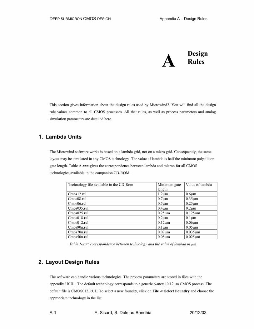
DEEP SUBMICRON CMOS DESIGN Appendix A – Design Rules A-1 E. Sicard, S. Delmas-Bendhia 20/12/03 A Design Rules This section gives information about the design rules used by Microwind2. You will find all the design rule values common to all CMOS processes. All that rules, as well as process parameters and analog simulation parameters are detailed here. 1. Lambda Units The Microwind software works is based on a lambda grid, not on a micro grid. Consequently, the same layout may be simulated in any CMOS technology. The value of lambda is half the minimum polysilicon gate length. Table A-xxx gives the correspondence between lambda and micron for all CMOS technologies available in the companion CD-ROM. Technology file available in the CD-Rom Minimum gate length Value of lambda Cmos12.rul 1.2μm 0.6μm Cmos08.rul 0.7μm 0.35μm Cmos06.rul 0.5μm 0.25μm Cmos035.rul 0.4μm 0.2μm Cmos025.rul 0.25μm 0.125μm Cmos018.rul 0.2μm 0.1μm Cmos012.rul 0.12μm 0.06μm Cmos90n.rul 0.1μm 0.05μm Cmos70n.rul 0.07μm 0.035μm Cmos50n.rul 0.05μm 0.025μm Table 1-xxx: correspondence between technology and the value of lambda in μm 2. Layout Design Rules The software can handle various technologies. The process parameters are stored in files with the appendix '.RUL'. The default technology corresponds to a generic 6-metal 0.12μm CMOS process. The default file is CMOS012.RUL. To select a new foundry, click on File -> Select Foundry and choose the appropriate technology in the list.
Transcript of A Design Rules - Electrical and Computer Engineeringandreou/216/Archives/2010/Handouts/... · DEEP...
DEEP SUBMICRON CMOS DESIGN Appendix A – Design Rules
A-1 E. Sicard, S. Delmas-Bendhia 20/12/03
A Design Rules
This section gives information about the design rules used by Microwind2. You will find all the design
rule values common to all CMOS processes. All that rules, as well as process parameters and analog
simulation parameters are detailed here.
1. Lambda Units
The Microwind software works is based on a lambda grid, not on a micro grid. Consequently, the same
layout may be simulated in any CMOS technology. The value of lambda is half the minimum polysilicon
gate length. Table A-xxx gives the correspondence between lambda and micron for all CMOS
technologies available in the companion CD-ROM.
Technology file available in the CD-Rom Minimum gate
length Value of lambda
Cmos12.rul 1.2µm 0.6µm Cmos08.rul 0.7µm 0.35µm Cmos06.rul 0.5µm 0.25µm Cmos035.rul 0.4µm 0.2µm Cmos025.rul 0.25µm 0.125µm Cmos018.rul 0.2µm 0.1µm Cmos012.rul 0.12µm 0.06µm Cmos90n.rul 0.1µm 0.05µm Cmos70n.rul 0.07µm 0.035µm Cmos50n.rul 0.05µm 0.025µm
Table 1-xxx: correspondence between technology and the value of lambda in µm
2. Layout Design Rules
The software can handle various technologies. The process parameters are stored in files with the
appendix '.RUL'. The default technology corresponds to a generic 6-metal 0.12µm CMOS process. The
default file is CMOS012.RUL. To select a new foundry, click on File -> Select Foundry and choose the
appropriate technology in the list.
DEEP SUBMICRON CMOS DESIGN Appendix A – Design Rules
A-2 E. Sicard, S. Delmas-Bendhia 20/12/03
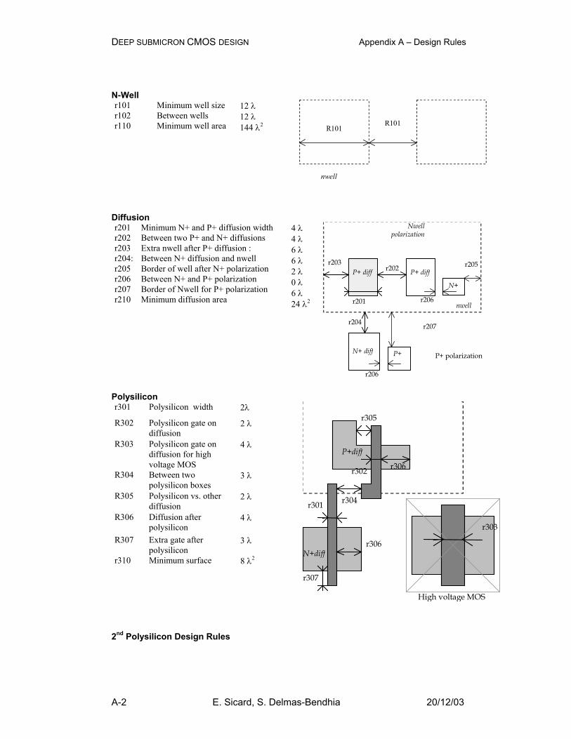
N-Well r101 r102 r110
Minimum well size Between wells Minimum well area
12 λ 12 λ 144 λ2 R101
R101
nwell
Diffusion r201 r202 r203 r204: r205 r206 r207 r210
Minimum N+ and P+ diffusion width Between two P+ and N+ diffusions Extra nwell after P+ diffusion : Between N+ diffusion and nwell Border of well after N+ polarization Between N+ and P+ polarization Border of Nwell for P+ polarization Minimum diffusion area
4 λ 4 λ 6 λ 6 λ 2 λ 0 λ 6 λ 24 λ2 nwell
P+ diff P+ diff
N+ diff
r204
r202r203
r201
P+ P+ polarization
r207
N+
r205
Nwellpolarization
r206
r206
Polysilicon r301 Polysilicon width 2λ
R302 Polysilicon gate on diffusion
2 λ
R303 Polysilicon gate on diffusion for high voltage MOS
4 λ
R304 Between two polysilicon boxes
3 λ
R305 Polysilicon vs. other diffusion
2 λ
R306 Diffusion after polysilicon
4 λ
R307 Extra gate after polysilicon
3 λ
r310 Minimum surface 8 λ2
P+diff
r305
r302 r306
N+diff
r304r301
r306
r307
r303
High voltage MOS
2nd Polysilicon Design Rules
DEEP SUBMICRON CMOS DESIGN Appendix A – Design Rules
A-3 E. Sicard, S. Delmas-Bendhia 20/12/03
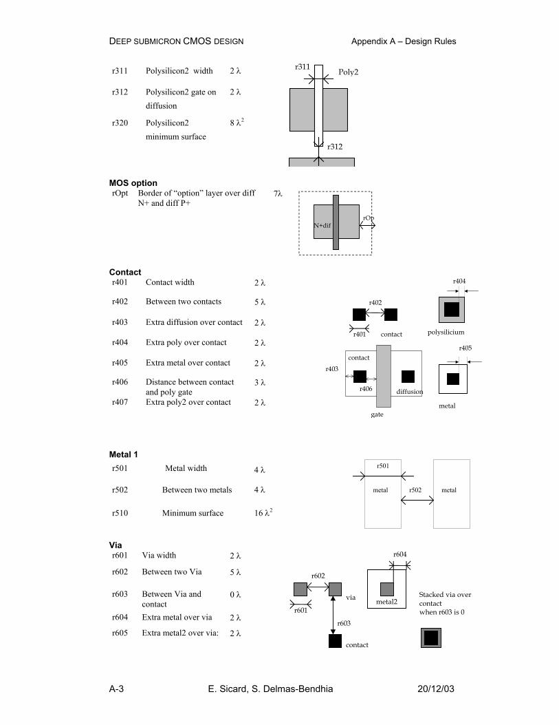
r311 Polysilicon2 width 2 λ
r312 Polysilicon2 gate on diffusion
2 λ
r320 Polysilicon2 minimum surface
8 λ2
Poly2r311
r312
MOS option rOpt
Border of “option” layer over diff N+ and diff P+
7λ
N+difrOp
Contact r401 Contact width 2 λ
r402 Between two contacts 5 λ
r403
Extra diffusion over contact 2 λ
r404 Extra poly over contact 2 λ
r405 Extra metal over contact 2 λ
r406 Distance between contact and poly gate
3 λ
r407 Extra poly2 over contact 2 λ
r401
r402
contact polysilicium
r404
contact
gate
diffusion
r403
r406
metal
r405
Metal 1 r501 Metal width 4 λ
r502 Between two metals 4 λ
r510 Minimum surface 16 λ2
metal
r501
metalr502
Via r601 Via width 2 λ
r602 Between two Via 5 λ
r603 Between Via and contact
0 λ
r604 Extra metal over via 2 λ
r605 Extra metal2 over via: 2 λ
r601
r602
via metal2
r604
contact
r603
Stacked via overcontactwhen r603 is 0
DEEP SUBMICRON CMOS DESIGN Appendix A – Design Rules
A-4 E. Sicard, S. Delmas-Bendhia 20/12/03
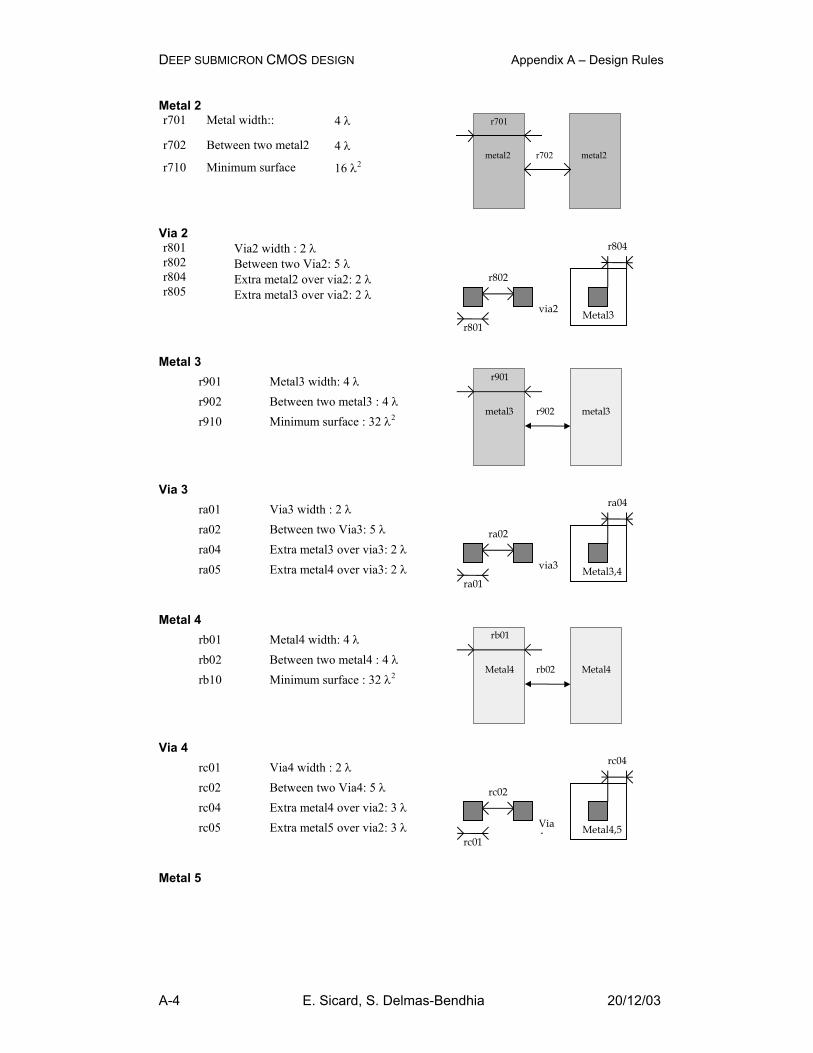
Metal 2 r701 Metal width:: 4 λ
r702 Between two metal2 4 λ
r710 Minimum surface 16 λ2 metal2
r701
metal2r702
Via 2 r801 r802 r804 r805
Via2 width : 2 λ Between two Via2: 5 λ Extra metal2 over via2: 2 λ Extra metal3 over via2: 2 λ r801
r802
via2 Metal3
r804
Metal 3 r901 r902 r910
Metal3 width: 4 λ Between two metal3 : 4 λ Minimum surface : 32 λ2
metal3
r901
metal3r902
Via 3 ra01 ra02 ra04 ra05
Via3 width : 2 λ Between two Via3: 5 λ Extra metal3 over via3: 2 λ Extra metal4 over via3: 2 λ ra01
ra02
via3 Metal3,4
ra04
Metal 4 rb01 rb02 rb10
Metal4 width: 4 λ Between two metal4 : 4 λ Minimum surface : 32 λ2
Metal4
rb01
Metal4rb02
Via 4 rc01 rc02 rc04 rc05
Via4 width : 2 λ Between two Via4: 5 λ Extra metal4 over via2: 3 λ Extra metal5 over via2: 3 λ rc01
rc02
Via4 Metal4,5
rc04
Metal 5
DEEP SUBMICRON CMOS DESIGN Appendix A – Design Rules
A-5 E. Sicard, S. Delmas-Bendhia 20/12/03
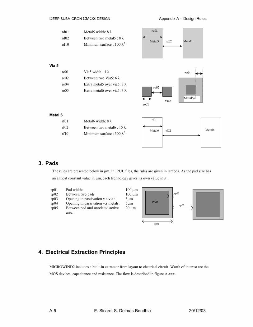
rd01 rd02 rd10
Metal5 width: 8 λ Between two metal5 : 8 λ Minimum surface : 100 λ2
Metal5
rd01
Metal5rd02
Via 5 re01 re02 re04 re05
Via5 width : 4 λ Between two Via5: 6 λ Extra metal5 over via5: 3 λ Extra metal6 over via5: 3 λ re01
re02
Via5Metal5,6
re04
Metal 6 rf01 rf02 rf10
Metal6 width: 8 λ Between two metal6 : 15 λ Minimum surface : 300 λ2
Metal6
rf01
Metal6rf02
3. Pads The rules are presented below in µm. In .RUL files, the rules are given in lambda. As the pad size has
an almost constant value in µm, each technology gives its own value in λ.
rp01 rp02 rp03 rp04 rp05
Pad width: Between two pads Opening in passivation v.s via : Opening in passivation v.s metals: Between pad and unrelated active area :
100 µm 100 µm 5µm 5µm 20 µm
PAD
rp03
rp01
rp02
4. Electrical Extraction Principles
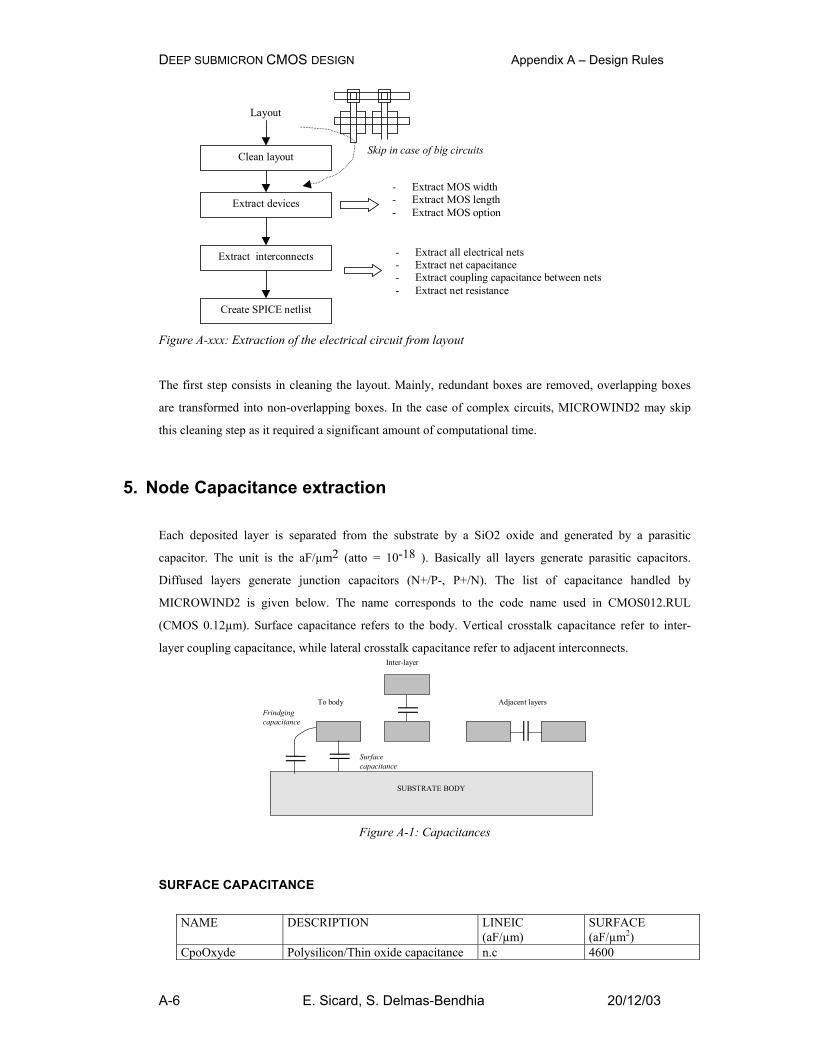
MICROWIND2 includes a built-in extractor from layout to electrical circuit. Worth of interest are the
MOS devices, capacitance and resistance. The flow is described in figure A-xxx.
DEEP SUBMICRON CMOS DESIGN Appendix A – Design Rules
A-6 E. Sicard, S. Delmas-Bendhia 20/12/03
Layout
Extract devices
Extract interconnects
- Extract MOS width- Extract MOS length- Extract MOS option
- Extract all electrical nets- Extract net capacitance- Extract coupling capacitance between nets- Extract net resistance
Create SPICE netlist
Clean layout Skip in case of big circuits
Figure A-xxx: Extraction of the electrical circuit from layout
The first step consists in cleaning the layout. Mainly, redundant boxes are removed, overlapping boxes
are transformed into non-overlapping boxes. In the case of complex circuits, MICROWIND2 may skip
this cleaning step as it required a significant amount of computational time.
5. Node Capacitance extraction
Each deposited layer is separated from the substrate by a SiO2 oxide and generated by a parasitic
capacitor. The unit is the aF/µm2 (atto = 10-18 ). Basically all layers generate parasitic capacitors.
Diffused layers generate junction capacitors (N+/P-, P+/N). The list of capacitance handled by
MICROWIND2 is given below. The name corresponds to the code name used in CMOS012.RUL
(CMOS 0.12µm). Surface capacitance refers to the body. Vertical crosstalk capacitance refer to inter-
layer coupling capacitance, while lateral crosstalk capacitance refer to adjacent interconnects.
SUBSTRATE BODY
To body
Inter-layer
Adjacent layers
Surfacecapacitance
Frindgingcapacitance
Figure A-1: Capacitances
SURFACE CAPACITANCE
NAME DESCRIPTION LINEIC
(aF/µm) SURFACE (aF/µm2)
CpoOxyde Polysilicon/Thin oxide capacitance n.c 4600
DEEP SUBMICRON CMOS DESIGN Appendix A – Design Rules
A-7 E. Sicard, S. Delmas-Bendhia 20/12/03
CpoBody Polysilicon to substrate capacitance n.c 80 CMEBody Metal on thick oxide to substrate 42 28 CM2Body Metal2 on body 36 13 CM3Body Metal3 on body 33 10 CM4Body Metal4 on body 30 6 CM5Body Metal5 on body 30 5 CM6Body Metal6 on body 30 4
INTER-LAYER CROSSTALK CAPACITANCE NAME DESCRIPTION VALUE (aF/µm2) CM2Me Metal2 on metal 1 50 CM3M2 Metal3 on metal 2 50 CM4M3 Metal4 on metal 3 50 CM5M4 Metal5 on metal 4 50 CM6M5 Metal6 on metal 5 50
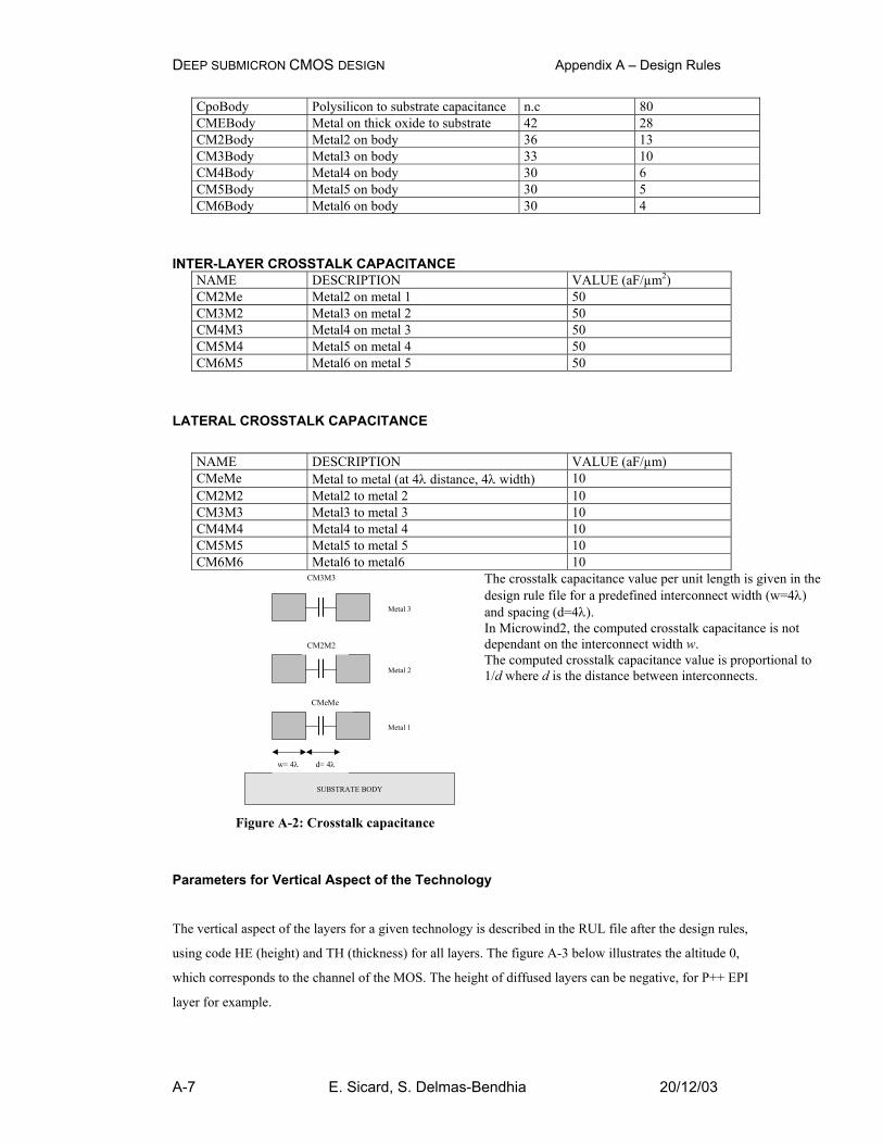
LATERAL CROSSTALK CAPACITANCE
NAME DESCRIPTION VALUE (aF/µm) CMeMe Metal to metal (at 4λ distance, 4λ width) 10 CM2M2 Metal2 to metal 2 10 CM3M3 Metal3 to metal 3 10 CM4M4 Metal4 to metal 4 10 CM5M5 Metal5 to metal 5 10 CM6M6 Metal6 to metal6 10
SUBSTRATE BODY
Metal 1
w= 4λ d= 4λ
Metal 2
Metal 3
CMeMe
CM2M2
CM3M3
Figure A-2: Crosstalk capacitance
The crosstalk capacitance value per unit length is given in the design rule file for a predefined interconnect width (w=4λ) and spacing (d=4λ). In Microwind2, the computed crosstalk capacitance is not dependant on the interconnect width w. The computed crosstalk capacitance value is proportional to 1/d where d is the distance between interconnects.
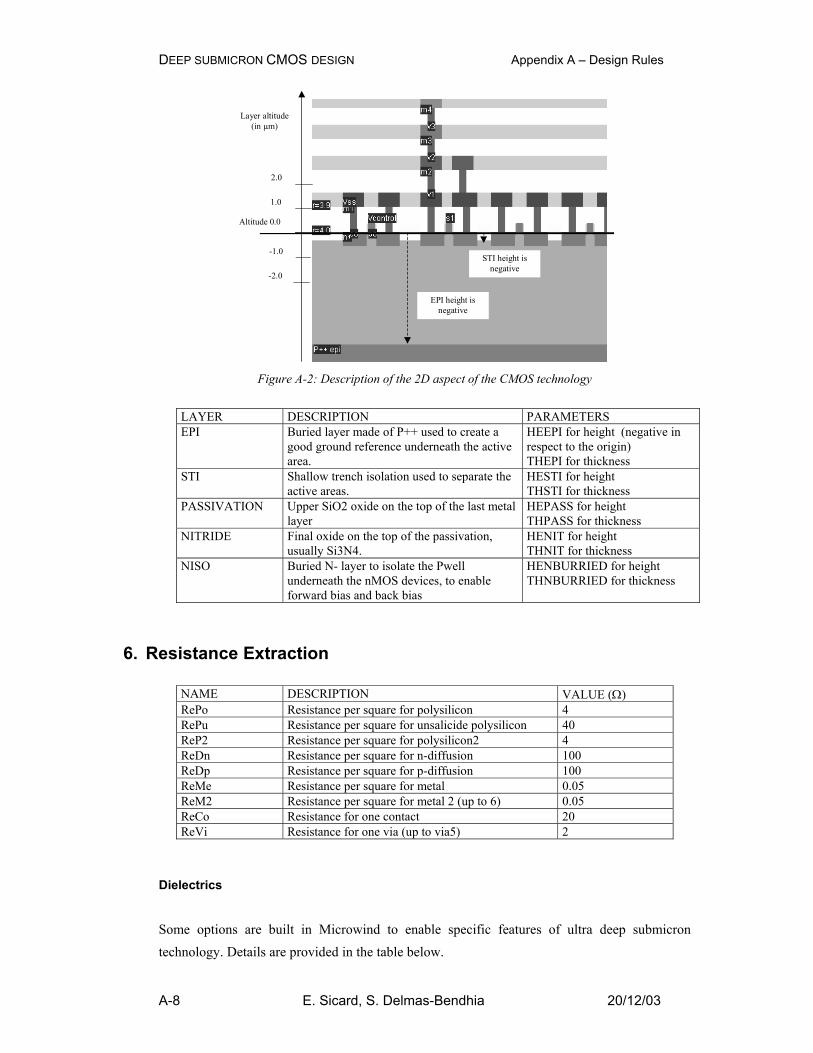
Parameters for Vertical Aspect of the Technology
The vertical aspect of the layers for a given technology is described in the RUL file after the design rules,
using code HE (height) and TH (thickness) for all layers. The figure A-3 below illustrates the altitude 0,
which corresponds to the channel of the MOS. The height of diffused layers can be negative, for P++ EPI
layer for example.
DEEP SUBMICRON CMOS DESIGN Appendix A – Design Rules
A-8 E. Sicard, S. Delmas-Bendhia 20/12/03
Altitude 0.0
1.0
2.0
-2.0
-1.0
EPI height isnegative
STI height isnegative
Layer altitude(in µm)
Figure A-2: Description of the 2D aspect of the CMOS technology
LAYER DESCRIPTION PARAMETERS EPI Buried layer made of P++ used to create a
good ground reference underneath the active area.
HEEPI for height (negative in respect to the origin) THEPI for thickness
STI Shallow trench isolation used to separate the active areas.
HESTI for height THSTI for thickness
PASSIVATION Upper SiO2 oxide on the top of the last metal layer
HEPASS for height THPASS for thickness
NITRIDE Final oxide on the top of the passivation, usually Si3N4.
HENIT for height THNIT for thickness
NISO Buried N- layer to isolate the Pwell underneath the nMOS devices, to enable forward bias and back bias
HENBURRIED for height THNBURRIED for thickness
6. Resistance Extraction
NAME DESCRIPTION VALUE (Ω) RePo Resistance per square for polysilicon 4 RePu Resistance per square for unsalicide polysilicon 40 ReP2 Resistance per square for polysilicon2 4 ReDn Resistance per square for n-diffusion 100 ReDp Resistance per square for p-diffusion 100 ReMe Resistance per square for metal 0.05 ReM2 Resistance per square for metal 2 (up to 6) 0.05 ReCo Resistance for one contact 20 ReVi Resistance for one via (up to via5) 2
Dielectrics Some options are built in Microwind to enable specific features of ultra deep submicron technology. Details are provided in the table below.
DEEP SUBMICRON CMOS DESIGN Appendix A – Design Rules
A-9 E. Sicard, S. Delmas-Bendhia 20/12/03
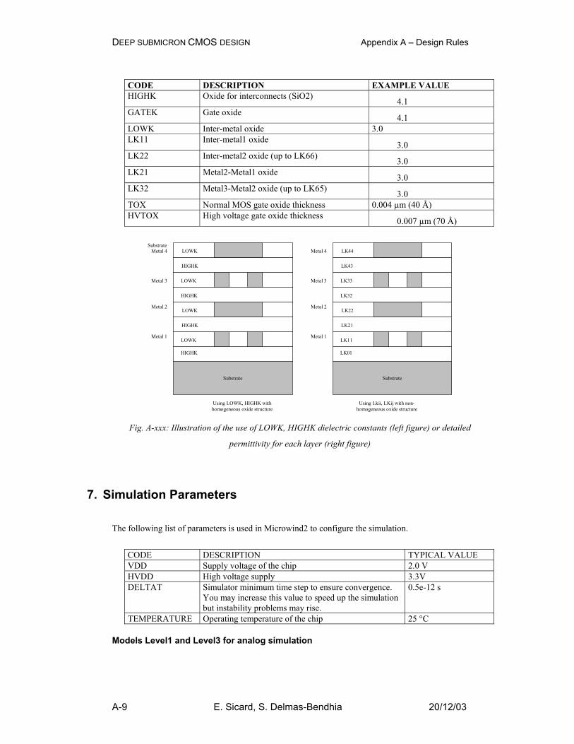
CODE DESCRIPTION EXAMPLE VALUE HIGHK Oxide for interconnects (SiO2) 4.1 GATEK Gate oxide 4.1 LOWK Inter-metal oxide 3.0 LK11 Inter-metal1 oxide 3.0 LK22 Inter-metal2 oxide (up to LK66) 3.0 LK21 Metal2-Metal1 oxide 3.0 LK32 Metal3-Metal2 oxide (up to LK65) 3.0 TOX Normal MOS gate oxide thickness 0.004 µm (40 Å) HVTOX High voltage gate oxide thickness 0.007 µm (70 Å)
Substrate
Substrate
Metal 1LK11
LK21
LK22
LK33
LK43
LK44
Metal 2
LK32
Metal 3
Metal 4
LK01
Substrate
Metal 1LOWK
HIGHK
LOWK
LOWK
HIGHK
LOWK
Metal 2
HIGHK
Metal 3
Metal 4
HIGHK
Using LOWK, HIGHK withhomogeneous oxide structure
Using Lkii, LKij with non-homogeneous oxide structure
Fig. A-xxx: Illustration of the use of LOWK, HIGHK dielectric constants (left figure) or detailed
permittivity for each layer (right figure)
7. Simulation Parameters The following list of parameters is used in Microwind2 to configure the simulation.
CODE DESCRIPTION TYPICAL VALUE VDD Supply voltage of the chip 2.0 V HVDD High voltage supply 3.3V DELTAT Simulator minimum time step to ensure convergence.
You may increase this value to speed up the simulation but instability problems may rise.
0.5e-12 s
TEMPERATURE Operating temperature of the chip 25 °C
Models Level1 and Level3 for analog simulation
DEEP SUBMICRON CMOS DESIGN Appendix A – Design Rules
A-10 E. Sicard, S. Delmas-Bendhia 20/12/03
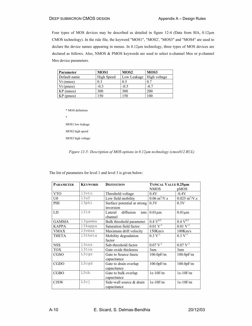
Four types of MOS devices may be described as detailed in figure 12-4 (Data from SIA, 0.12µm
CMOS technology). In the rule file, the keyword "MOS1", "MOS2', "MOS3" and "MOS4" are used to
declare the device names appearing in menus. In 0.12µm technology, three types of MOS devices are
declared as follows. Also, NMOS & PMOS keywords are used to select n-channel Mos or p-channel
Mos device parameters.
Parameter MOS1 MOS2 MOS3 Default name High Speed Low Leakage High voltage Vt (nmos) 0.3 0.5 0.7 Vt (pmos) -0.3 -0.5 -0.7 KP (nmos) 300 300 200 KP (pmos) 150 150 100
* MOS definition
*
MOS1 low leakage
MOS2 high speed
MOS3 high voltage
Figure 12-5: Description of MOS options in 0.12µm technology (cmos012.RUL)
The list of parameters for level 1 and level 3 is given below:
PARAMETER KEYWORD DEFINITION TYPICAL VALUE 0.25µm NMOS pMOS VTO l3vto Threshold voltage 0.4V -0.4V U0 l3u0 Low field mobility 0.06 m2/V.s 0.025 m2/V.s PHI l3phi Surface potential at strong
inversion 0.3V 0.3V
LD l3ld Lateral diffusion into channel
0.01µm 0.01µm
GAMMA l3gamma Bulk threshold parameter 0.4 V0.5 0.4 V0.5 KAPPA l3kappa Saturation field factor 0.01 V-1 0.01 V-1 VMAX l3vmax Maximum drift velocity 150Km/s 100Km/s THETA l3theta Mobility degradation
factor 0.3 V-1 0.3 V-1
NSS l3nss Sub-threshold factor 0.07 V-1 0.07 V-1 TOX l3tox Gate oxide thickness 3nm 3nm CGSO L3cgs Gate to Source lineic
capacitance 100.0pF/m 100.0pF/m
CGDO L3cgd Gate to drain overlap capacitance
100.0pF/m 100.0pF/m
CGBO L3cb Gate to bulk overlap capacitance
1e-10F/m 1e-10F/m
CJSW L3cj Side-wall source & drain capacitance
1e-10F/m 1e-10F/m
DEEP SUBMICRON CMOS DESIGN Appendix A – Design Rules
A-11 E. Sicard, S. Delmas-Bendhia 20/12/03
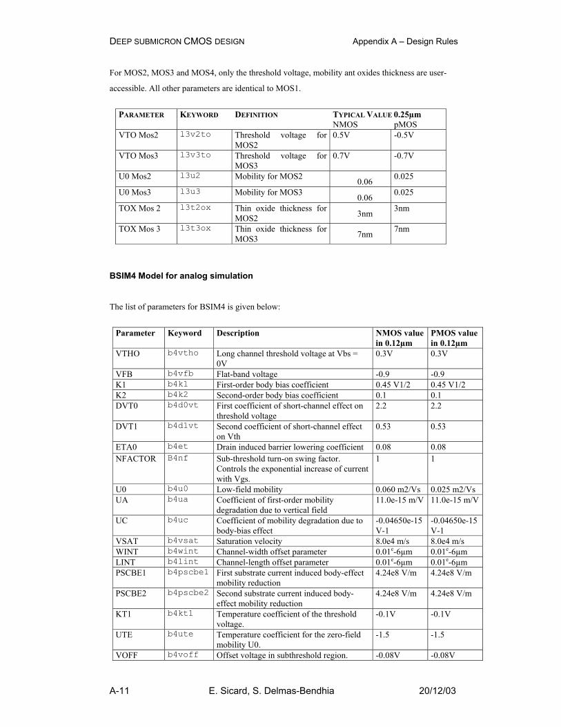
For MOS2, MOS3 and MOS4, only the threshold voltage, mobility ant oxides thickness are user-
accessible. All other parameters are identical to MOS1.
PARAMETER KEYWORD DEFINITION TYPICAL VALUE 0.25µm NMOS pMOS VTO Mos2 l3v2to Threshold voltage for
MOS2 0.5V -0.5V
VTO Mos3 l3v3to Threshold voltage for MOS3
0.7V -0.7V
U0 Mos2 l3u2 Mobility for MOS2 0.06 0.025
U0 Mos3 l3u3 Mobility for MOS3 0.06 0.025
TOX Mos 2 l3t2ox Thin oxide thickness for MOS2 3nm 3nm
TOX Mos 3 l3t3ox Thin oxide thickness for MOS3 7nm 7nm
BSIM4 Model for analog simulation
The list of parameters for BSIM4 is given below:
Parameter Keyword Description NMOS value
in 0.12µm PMOS value in 0.12µm
VTHO b4vtho Long channel threshold voltage at Vbs = 0V
0.3V 0.3V
VFB b4vfb Flat-band voltage -0.9 -0.9 K1 b4k1 First-order body bias coefficient 0.45 V1/2 0.45 V1/2 K2 b4k2 Second-order body bias coefficient 0.1 0.1 DVT0 b4d0vt First coefficient of short-channel effect on
threshold voltage 2.2 2.2
DVT1 b4d1vt Second coefficient of short-channel effect on Vth
0.53 0.53
ETA0 b4et Drain induced barrier lowering coefficient 0.08 0.08 NFACTOR B4nf Sub-threshold turn-on swing factor.
Controls the exponential increase of current with Vgs.
1 1
U0 b4u0 Low-field mobility 0.060 m2/Vs 0.025 m2/Vs UA b4ua Coefficient of first-order mobility
degradation due to vertical field 11.0e-15 m/V 11.0e-15 m/V
UC b4uc Coefficient of mobility degradation due to body-bias effect
-0.04650e-15 V-1
-0.04650e-15 V-1
VSAT b4vsat Saturation velocity 8.0e4 m/s 8.0e4 m/s WINT b4wint Channel-width offset parameter 0.01e-6µm 0.01e-6µm LINT b4lint Channel-length offset parameter 0.01e-6µm 0.01e-6µm PSCBE1
b4pscbe1 First substrate current induced body-effect mobility reduction
4.24e8 V/m 4.24e8 V/m
PSCBE2 b4pscbe2 Second substrate current induced body-effect mobility reduction
4.24e8 V/m 4.24e8 V/m
KT1 b4kt1 Temperature coefficient of the threshold voltage.
-0.1V -0.1V
UTE b4ute Temperature coefficient for the zero-field mobility U0.
-1.5 -1.5
VOFF b4voff Offset voltage in subthreshold region. -0.08V -0.08V
DEEP SUBMICRON CMOS DESIGN Appendix A – Design Rules
A-12 E. Sicard, S. Delmas-Bendhia 20/12/03
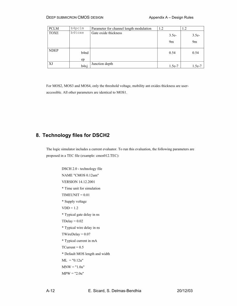
PCLM b4pclm Parameter for channel length modulation 1.2 1.2 TOXE b4toxe Gate oxide thickness 3.5e-
9m
3.5e-
9m
NDEP b4nd
ep
0.54 0.54
XJ b4xj Junction depth 1.5e-7 1.5e-7
For MOS2, MOS3 and MOS4, only the threshold voltage, mobility ant oxides thickness are user-
accessible. All other parameters are identical to MOS1.
8. Technology files for DSCH2
The logic simulator includes a current evaluator. To run this evaluation, the following parameters are
proposed in a TEC file (example: cmos012.TEC):
DSCH 2.0 - technology file
NAME "CMOS 0.12um"
VERSION 14.12.2001
* Time unit for simulation
TIMEUNIT = 0.01
* Supply voltage
VDD = 1.2
* Typical gate delay in ns
TDelay = 0.02
* Typical wire delay in ns
TWireDelay = 0.07
* Typical current in mA
TCurrent = 0.5
* Default MOS length and width
ML = "0.12u"
MNW = "1.0u"
MPW = "2.0u"
DEEP SUBMICRON CMOS DESIGN Appendix A – Design Rules
A-13 E. Sicard, S. Delmas-Bendhia 20/12/03
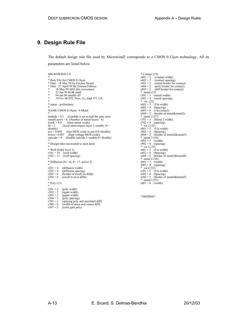
9. Design Rule File
The default design rule file used by Microwind2 corresponds to a CMOS 0.12µm technology. All its
parameters are listed below.
MICROWIND 2.0 * * Rule File for CMOS 0.18µm * Date : 18 May 98 by Etienne Sicard * Date : 27 April 99 By Etienne/Fabrice * 16 May 99 r603 dist via/contact * 23 Jun 99 KOR mm9 * 04 Jan 00 smaller dT * 19 Fev 00 STI, Niso, LL, high VT, LIL * * status : preliminary * NAME CMOS 0.18µm - 6 Metal * lambda = 0.1 (Lambda is set to half the gate size) metalLayers = 6 (Number of metal layers : 6) lowK = 4.0 (inter-metal oxide) lil = 1 (local interconnect layer 1=enable, 0= disable) tox = 0.004 (fast MOS oxide in µm 0.0=disable) hvtox= 0.007 (high voltage MOS oxide) salicide = 0 (Enable salicide 1=enable 0= disable) * * Design rules associated to each layer * * Well (Gds2 level 1) r101 = 10 (well width) r102 = 11 (well spacing) * * Diffusion (N+ 16, P+ 17, active 2) * r201 = 4 (diffusion width) r202 = 4 (diffusion spacing) r203 = 6 (border of nwell on diffp) r204 = 6 (nwell to next diffn) * * Poly (13) * r301 = 2 (poly width) r302 = 2 (ngate width) r303 = 2 (pgate width) r304 = 3 (poly spacing) r305 = 1 (spacing poly and unrelated diff) r306 = 4 (width of drain and source diff) r307 = 2 (extra gate poly)
* Contact (19) r401 = 2 (contact width) r402 = 3 (contact spacing) r403 = 2 (metal border for contact) r404 = 2 (poly border for contact) r405 = 2 (diff border for contact) * metal (23) r501 = 3 (metal width) r502 = 4 (metal spacing) * via (25) r601 = 3 (Via width) r602 = 4 (Spacing) r603 = 0 (via/contact) r604 = 2 (border of metal&metal2) * metal 2 (27) r701 = 3 (Metal 2 width) r702 = 4 (spacing) * via 2 (32) r801 = 3 (Via width) r802 = 4 (Spacing) r804 = 2 (border of metal2&metal3) * metal 3 (34) r901 = 3 (width) r902 = 4 (spacing) * via 3 (35) ra01 = 3 (Via width) ra02 = 4 (Spacing) ra04 = 2 (border of metal3&metal4) * metal 4 (36) rb01 = 3 (width) rb02 = 4 (spacing) * via 4 (52) rc01 = 3 (Via width) rc02 = 4 (Spacing) rc04 = 2 (border of metal4&metal5) * metal 5 (53) rd01 = 8 (width)
<section>
DEEP SUBMICRON CMOS DESIGN Appendix A – Design Rules
14 E.Sicard, S. Delmas-Bendhia 20/12/03
10. Simulation parameters for DSCH2
The following list of parameters is used in Dsch2 to configure the simulation.
CODE DESCRIPTION TYPICAL VALUE
VDD Supply voltage of the chip 2.0 V
<add default.rul>


![[T2RE] rules EL reprint 2015 TTR2 europe rules EN · Οι γκρι διαδρομές μπορούν να κλείσουν με ένα σετ ομοίων ... Μην ξεχνάτε](https://static.fdocument.org/doc/165x107/5f9cf751a63f0d1bd71c4e21/t2re-rules-el-reprint-2015-ttr2-europe-rules-en-.jpg)