6.976 High Speed Communication Circuits and Systems Lecture 20
48
6.976 High Speed Communication Circuits and Systems Lecture 20 Performance Measures of Wireless Communication Michael Perrott Massachusetts Institute of Technology Copyright © 2003 by Michael H. Perrott
Transcript of 6.976 High Speed Communication Circuits and Systems Lecture 20
6.976High Speed Communication Circuits and Systems
Lecture 20Performance Measures of Wireless Communication
Michael PerrottMassachusetts Institute of Technology
Copyright © 2003 by Michael H. Perrott
M.H. Perrott MIT OCW
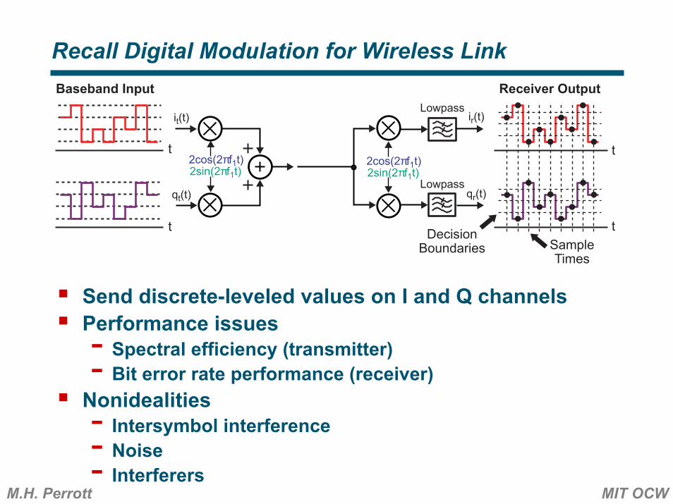
Recall Digital Modulation for Wireless Link
Send discrete-leveled values on I and Q channelsPerformance issues- Spectral efficiency (transmitter)- Bit error rate performance (receiver)Nonidealities- Intersymbol interference- Noise- Interferers
Receiver Output
2cos(2πf1t)2sin(2πf1t)
Lowpassir(t)
Lowpassqr(t)
it(t)
qt(t)
2cos(2πf1t)2sin(2πf1t)
t
t
t
Baseband Input
tDecisionBoundaries Sample
Times
M.H. Perrott MIT OCW
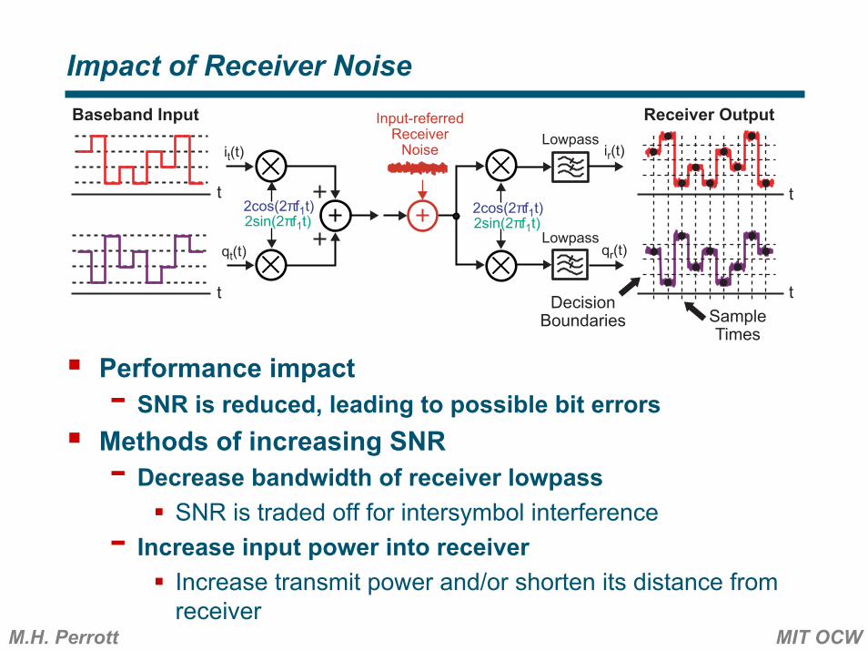
Impact of Receiver Noise
Performance impact- SNR is reduced, leading to possible bit errors
Methods of increasing SNR- Decrease bandwidth of receiver lowpass
SNR is traded off for intersymbol interference- Increase input power into receiver
Increase transmit power and/or shorten its distance from receiver
Receiver Output
2cos(2πf1t)2sin(2πf1t)
Lowpassir(t)
Lowpassqr(t)
it(t)
qt(t)
2cos(2πf1t)2sin(2πf1t)
t
t
t
Baseband Input
tDecisionBoundaries Sample
Times
Input-referredReceiver
Noise
M.H. Perrott MIT OCW
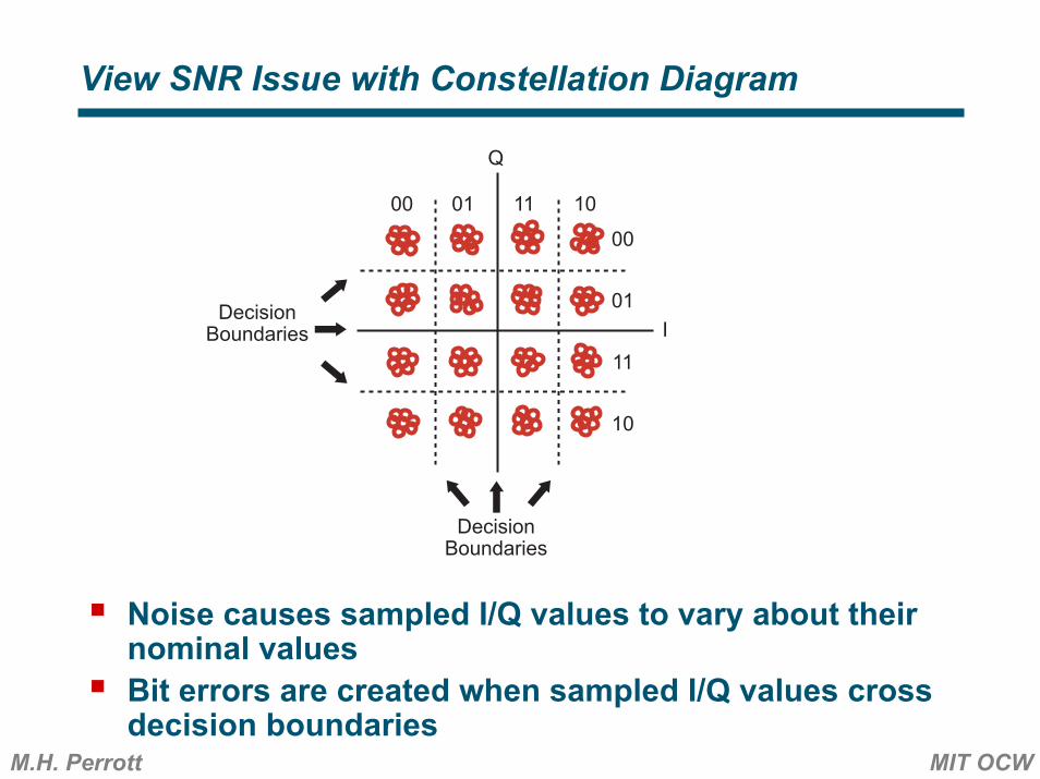
View SNR Issue with Constellation Diagram
Noise causes sampled I/Q values to vary about their nominal valuesBit errors are created when sampled I/Q values cross decision boundaries
DecisionBoundaries
DecisionBoundaries
00 01 11 10
00
01
11
10
I
Q
M.H. Perrott MIT OCW
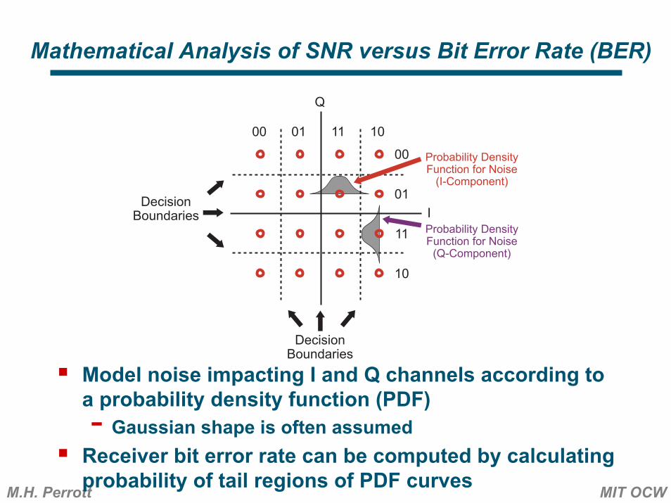
Mathematical Analysis of SNR versus Bit Error Rate (BER)
Model noise impacting I and Q channels according to a probability density function (PDF)- Gaussian shape is often assumed
Receiver bit error rate can be computed by calculating probability of tail regions of PDF curves
DecisionBoundaries
DecisionBoundaries
00 01 11 10
00
01
11
10
I
Q
Probability DensityFunction for Noise
(I-Component)
Probability DensityFunction for Noise
(Q-Component)
M.H. Perrott MIT OCW
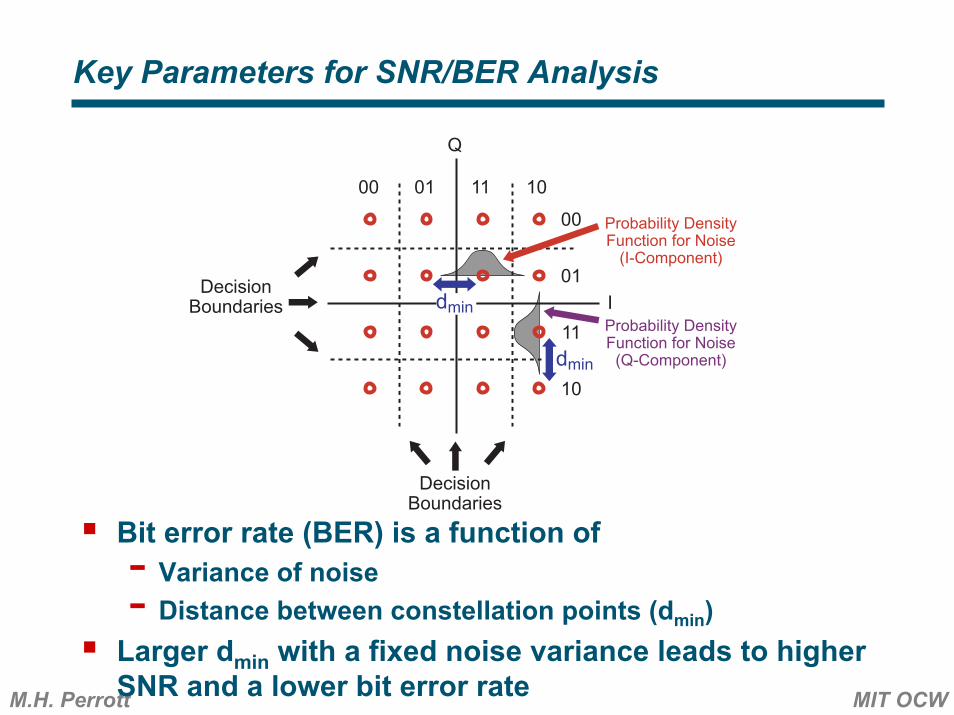
Key Parameters for SNR/BER Analysis
Bit error rate (BER) is a function of- Variance of noise- Distance between constellation points (dmin)
Larger dmin with a fixed noise variance leads to higher SNR and a lower bit error rate
DecisionBoundaries
DecisionBoundaries
00 01 11 10
00
01
11
10
I
Q
Probability DensityFunction for Noise
(I-Component)
Probability DensityFunction for Noise
(Q-Component)dmin
dmin
M.H. Perrott MIT OCW
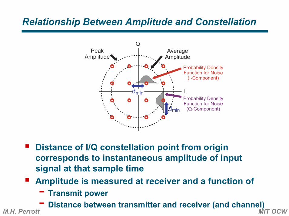
Relationship Between Amplitude and Constellation
Distance of I/Q constellation point from origin corresponds to instantaneous amplitude of input signal at that sample timeAmplitude is measured at receiver and a function of- Transmit power- Distance between transmitter and receiver (and channel)
PeakAmplitude
AverageAmplitude
I
Q
Probability DensityFunction for Noise
(I-Component)
Probability DensityFunction for Noise
(Q-Component)dmin
dmin
M.H. Perrott MIT OCW
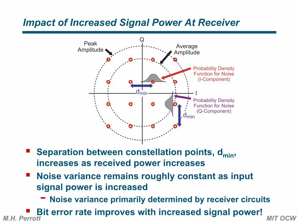
Impact of Increased Signal Power At Receiver
Separation between constellation points, dmin, increases as received power increasesNoise variance remains roughly constant as input signal power is increased- Noise variance primarily determined by receiver circuits
Bit error rate improves with increased signal power!
PeakAmplitude Average
Amplitude
I
Q
Probability DensityFunction for Noise
(I-Component)
Probability DensityFunction for Noise
(Q-Component)
dmin
dmin
M.H. Perrott MIT OCW
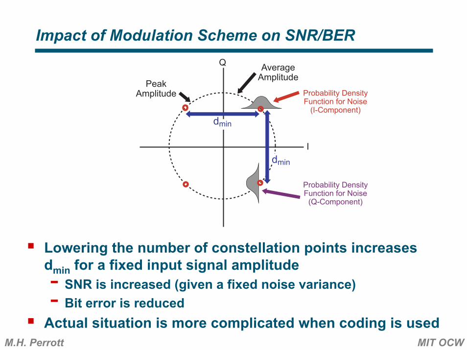
Impact of Modulation Scheme on SNR/BER
Lowering the number of constellation points increases dmin for a fixed input signal amplitude- SNR is increased (given a fixed noise variance)- Bit error is reduced
Actual situation is more complicated when coding is used
PeakAmplitude
AverageAmplitude
I
Q
Probability DensityFunction for Noise
(I-Component)
Probability DensityFunction for Noise
(Q-Component)
dmin
dmin
M.H. Perrott MIT OCW
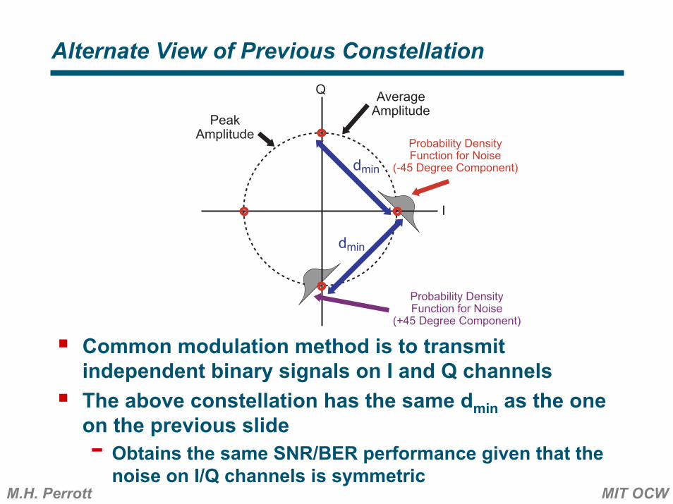
Alternate View of Previous Constellation
Common modulation method is to transmit independent binary signals on I and Q channelsThe above constellation has the same dmin as the one on the previous slide- Obtains the same SNR/BER performance given that the
noise on I/Q channels is symmetric
PeakAmplitude
AverageAmplitude
I
Q
Probability DensityFunction for Noise
(-45 Degree Component)
Probability DensityFunction for Noise
(+45 Degree Component)
dmin
dmin
M.H. Perrott MIT OCW
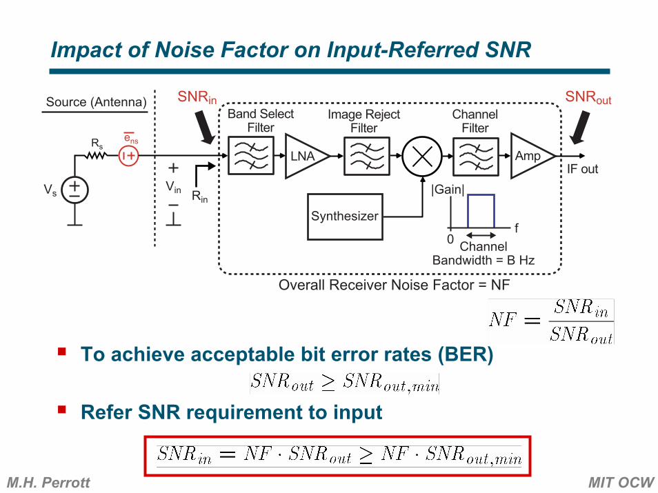
Impact of Noise Factor on Input-Referred SNR
To achieve acceptable bit error rates (BER)
Refer SNR requirement to input
Synthesizer
LNA
Image RejectFilter
ChannelFilter
Rsens
Source (Antenna)
Vs RinVin
0 ChannelBandwidth = B Hz
f
|Gain|
SNRin SNRout
Overall Receiver Noise Factor = NF
Amp
Band SelectFilter
IF out
M.H. Perrott MIT OCW
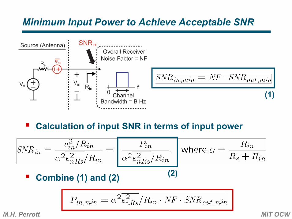
Minimum Input Power to Achieve Acceptable SNR
Calculation of input SNR in terms of input power
Combine (1) and (2)
(1)
(2)
Rsens
Source (Antenna)
Vs RinVin
0 ChannelBandwidth = B Hz
f
SNRinOverall Receiver
Noise Factor = NF
M.H. Perrott MIT OCW
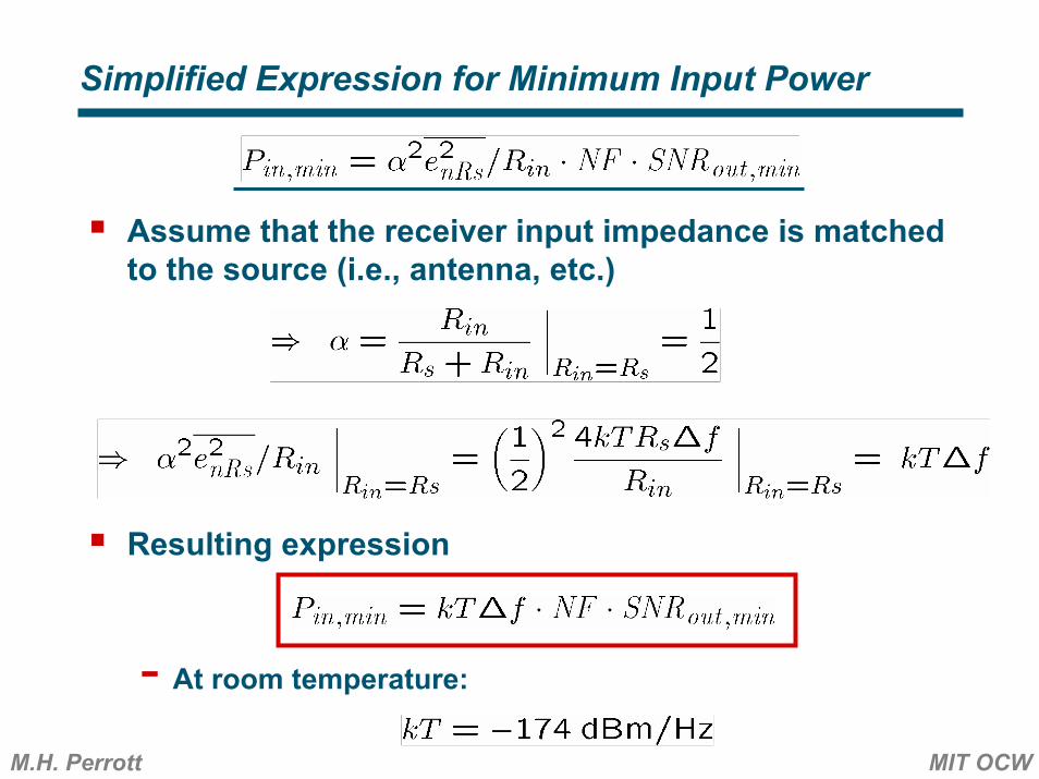
Simplified Expression for Minimum Input Power
Assume that the receiver input impedance is matched to the source (i.e., antenna, etc.)
Resulting expression
- At room temperature:
M.H. Perrott MIT OCW
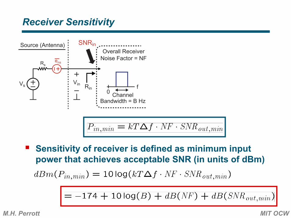
Sensitivity of receiver is defined as minimum input power that achieves acceptable SNR (in units of dBm)
Rsens
Source (Antenna)
Vs RinVin
0 ChannelBandwidth = B Hz
f
SNRinOverall Receiver
Noise Factor = NF
Receiver Sensitivity
M.H. Perrott MIT OCW
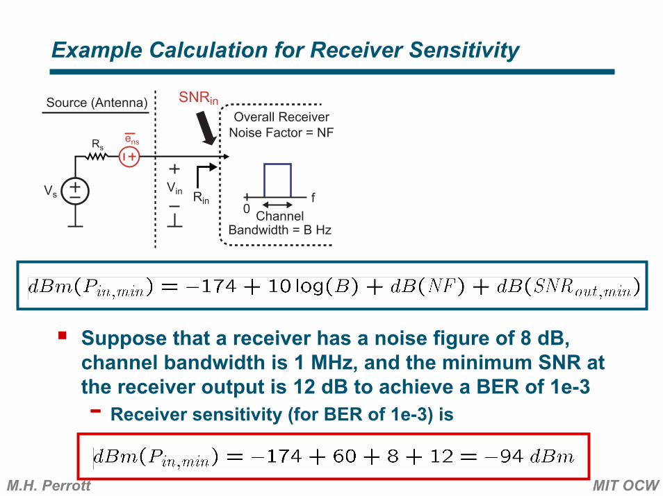
Suppose that a receiver has a noise figure of 8 dB, channel bandwidth is 1 MHz, and the minimum SNR at the receiver output is 12 dB to achieve a BER of 1e-3- Receiver sensitivity (for BER of 1e-3) is
Rsens
Source (Antenna)
Vs RinVin
0 ChannelBandwidth = B Hz
f
SNRinOverall Receiver
Noise Factor = NF
Example Calculation for Receiver Sensitivity
M.H. Perrott MIT OCW
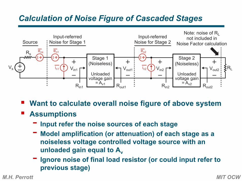
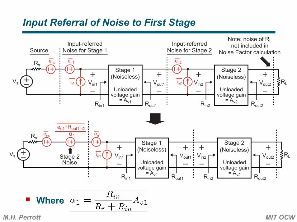
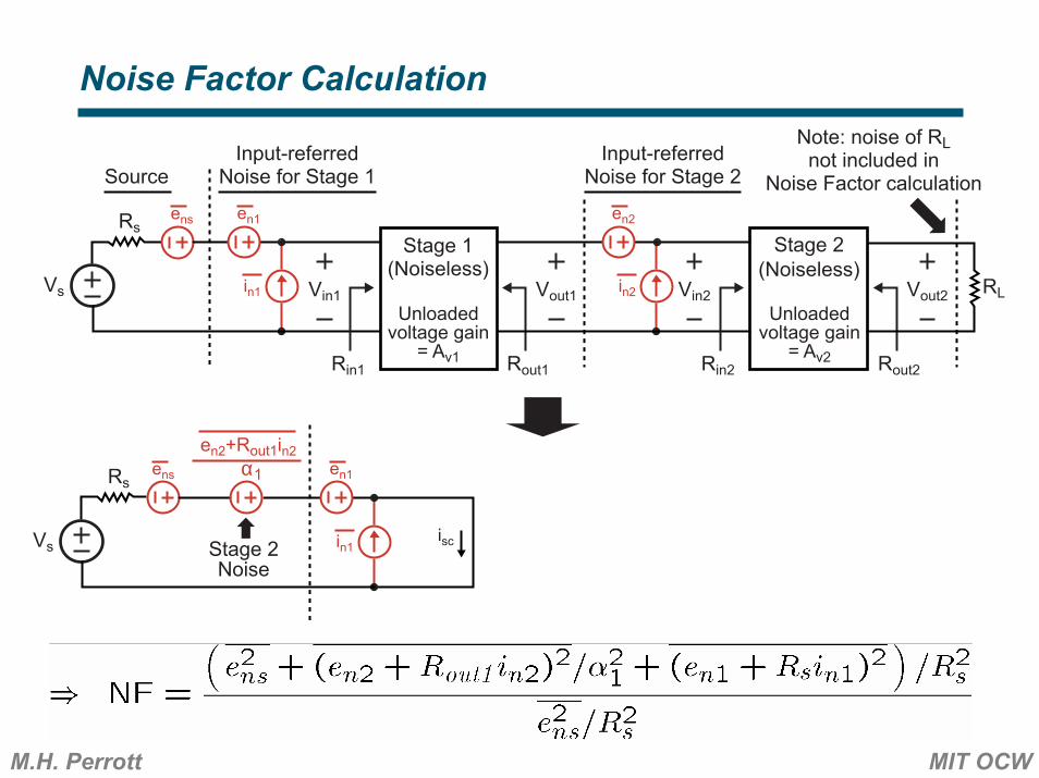
Calculation of Noise Figure of Cascaded Stages
Want to calculate overall noise figure of above systemAssumptions- Input refer the noise sources of each stage- Model amplification (or attenuation) of each stage as a
noiseless voltage controlled voltage source with an unloaded gain equal to Av- Ignore noise of final load resistor (or could input refer to previous stage)
Rsens
Source
Vs in1
en1
Vin1
Stage 1(Noiseless)
Vout1
Rin1 Rout1
in2
en2
Vin2 Vout2
Rin2 Rout2
RL
Input-referredNoise for Stage 1
Input-referredNoise for Stage 2
Note: noise of RLnot included in
Noise Factor calculation
Stage 2(Noiseless)
Unloadedvoltage gain
= Av1
Unloadedvoltage gain
= Av2
M.H. Perrott MIT OCW
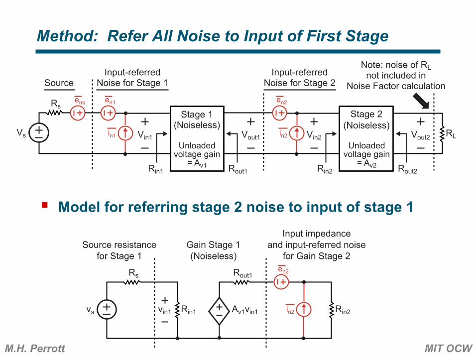
Method: Refer All Noise to Input of First Stage
Model for referring stage 2 noise to input of stage 1
Rsens
Source
Vs in1
en1
Vin1
Stage 1(Noiseless)
Vout1
Rin1 Rout1
in2
en2
Vin2 Vout2
Rin2 Rout2
RL
Input-referredNoise for Stage 1
Input-referredNoise for Stage 2
Note: noise of RLnot included in
Noise Factor calculation
Stage 2(Noiseless)
Unloadedvoltage gain
= Av1
Unloadedvoltage gain
= Av2
in2
en2
Rin2Av1vin1
Rout1
Rin1
Rs
vs
Gain Stage 1(Noiseless)
Input impedanceand input-referred noise
for Gain Stage 2Source resistance
for Stage 1
vin1
M.H. Perrott MIT OCW
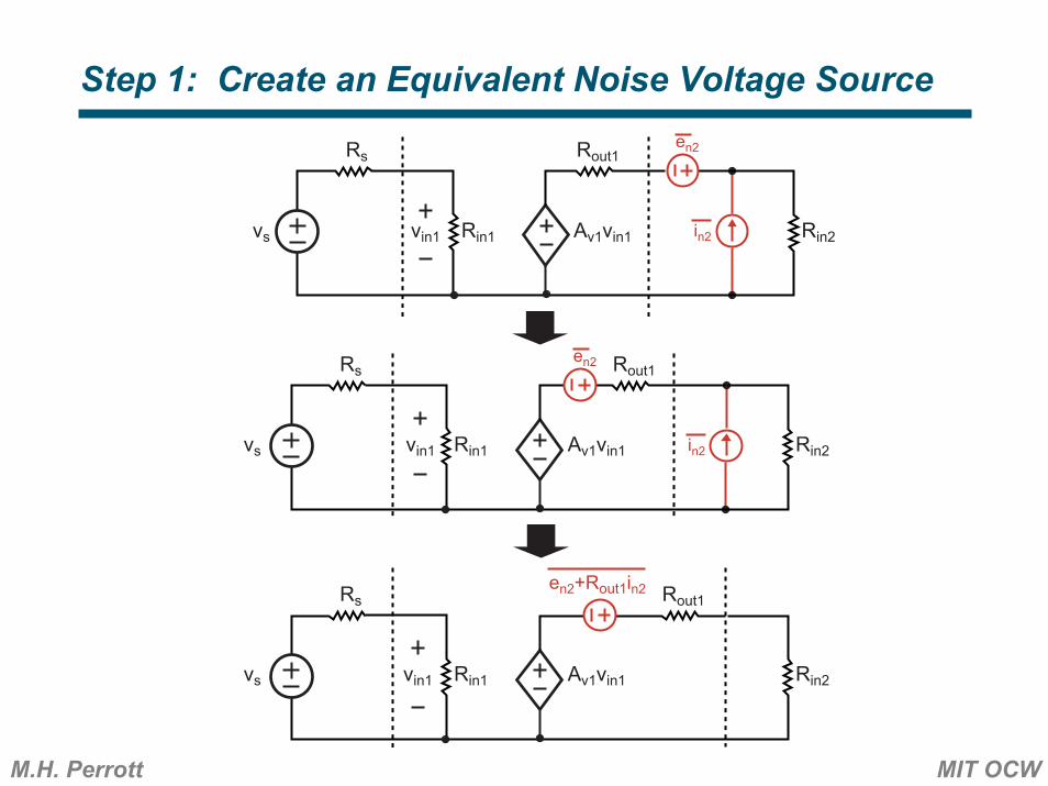
Step 1: Create an Equivalent Noise Voltage Source
in2
en2
Rin2Av1vin1
Rout1
Rin1
Rs
vs vin1
in2
en2
Rin2Av1vin1
Rout1
Rin1
Rs
vs vin1
en2+Rout1in2
Rin2Av1vin1
Rout1
Rin1
Rs
vs vin1
M.H. Perrott MIT OCW
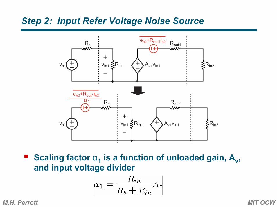
Step 2: Input Refer Voltage Noise Source
Scaling factor α1 is a function of unloaded gain, Av, and input voltage divider
en2+Rout1in2
Rin2Av1vin1
Rout1
Rin1
Rs
vs vin1
en2+Rout1in2
Rin2Av1vin1
Rout1
Rin1
Rs
vs vin1
α1
M.H. Perrott MIT OCW
Input Referral of Noise to First Stage
Where
Rsens
Vs in1
en1
Vin1
Stage 1(Noiseless)
Vout1
Rin1 Rout1
Vin2 Vout2
Rin2 Rout2
RLStage 2Noise
Stage 2(Noiseless)
Unloadedvoltage gain
= Av1
Unloadedvoltage gain
= Av2
en2+Rout1in2α1
Rsens
Source
Vs in1
en1
Vin1
Stage 1(Noiseless)
Vout1
Rin1 Rout1
in2
en2
Vin2 Vout2
Rin2 Rout2
RL
Input-referredNoise for Stage 1
Input-referredNoise for Stage 2
Note: noise of RLnot included in
Noise Factor calculation
Stage 2(Noiseless)
Unloadedvoltage gain
= Av1
Unloadedvoltage gain
= Av2
M.H. Perrott MIT OCW
Noise Factor Calculation
Rsens
Vs in1
en1
Stage 2Noise
en2+Rout1in2α1
Rsens
Source
Vs in1
en1
Vin1
Stage 1(Noiseless)
Vout1
Rin1 Rout1
in2
en2
Vin2 Vout2
Rin2 Rout2
RL
Input-referredNoise for Stage 1
Input-referredNoise for Stage 2
Note: noise of RLnot included in
Noise Factor calculation
Stage 2(Noiseless)
Unloadedvoltage gain
= Av1
Unloadedvoltage gain
= Av2
isc
M.H. Perrott MIT OCW
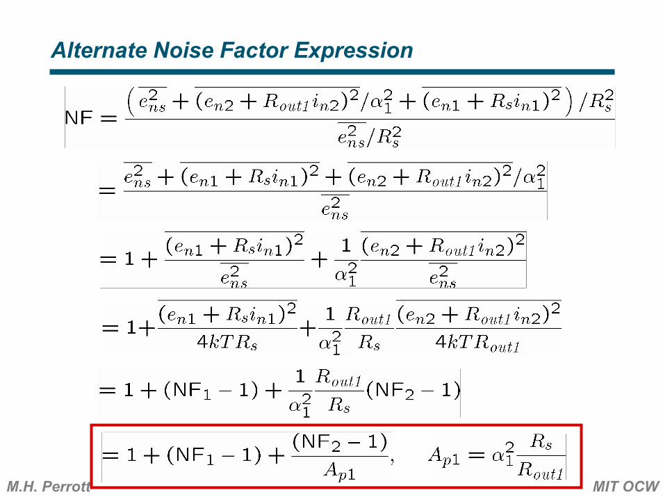
Alternate Noise Factor Expression
M.H. Perrott MIT OCW
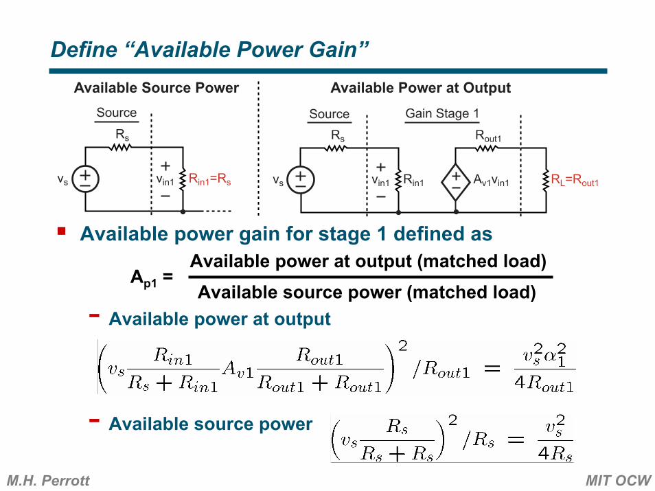
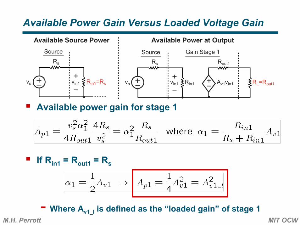
Define “Available Power Gain”
Available power gain for stage 1 defined as
- Available power at output
- Available source power
Available power at output (matched load)Available source power (matched load)
RL=Rout1Av1vin1
Rout1
Rin1
Rs
vs
Gain Stage 1
vin1Rin1=Rs
Rs
vs
Source
vin1
Available Source Power Available Power at OutputSource
Ap1 =
M.H. Perrott MIT OCW
Available Power Gain Versus Loaded Voltage Gain
Available power gain for stage 1
If Rin1 = Rout1 = Rs
- Where Av1_l is defined as the “loaded gain” of stage 1
RL=Rout1Av1vin1
Rout1
Rin1
Rs
vs
Gain Stage 1
vin1Rin1=Rs
Rs
vs
Source
vin1
Available Source Power Available Power at OutputSource
M.H. Perrott MIT OCW
Final Expressions for Cascaded Noise Factor Calculation
Overall Noise Factor (general expression)
Overall Noise Factor when all input and output impedances equal Rs:
Rsens
Source
Vs
Stage 1
Rin1 Rout1
Vout RL
Note: noise of RLnot included in
Noise Factor calculation
Unloadedvoltage gain
= Av1
NF1
Stage 2
Rin2 Rout2
Unloadedvoltage gain
= Av2
NF2
Stage k
Rink Routk
Unloadedvoltage gain
= Avk
NFk
M.H. Perrott MIT OCW
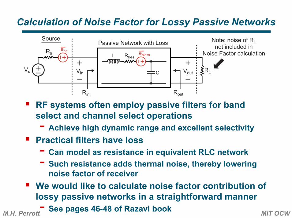
Calculation of Noise Factor for Lossy Passive Networks
RF systems often employ passive filters for band select and channel select operations- Achieve high dynamic range and excellent selectivity
Practical filters have loss- Can model as resistance in equivalent RLC network- Such resistance adds thermal noise, thereby lowering
noise factor of receiverWe would like to calculate noise factor contribution of lossy passive networks in a straightforward manner- See pages 46-48 of Razavi book
Vin
Rin
Vout
Rout
RL
L
C
Rsens
Source
Vs
Passive Network with Loss Note: noise of RLnot included in
Noise Factor calculationenlossRloss
M.H. Perrott MIT OCW
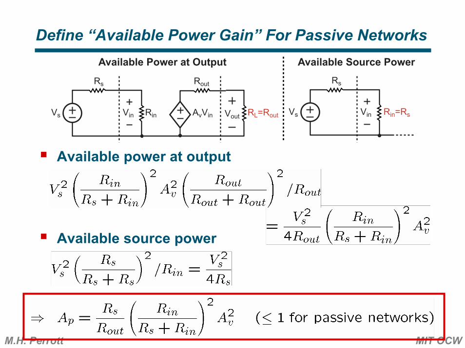
Define “Available Power Gain” For Passive Networks
Available power at output
Available source power
RL=RoutAvVin
Rout
Rin
Rs
Vs Vin Rin=Rs
Rs
Vs Vin
Available Source PowerAvailable Power at Output
Vout
M.H. Perrott MIT OCW
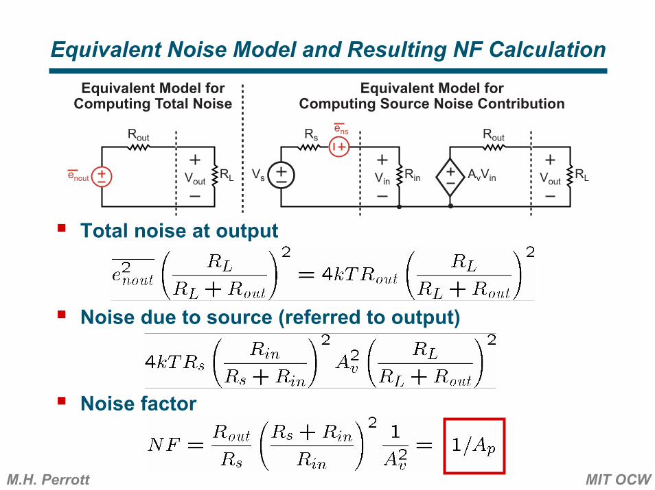
Equivalent Noise Model and Resulting NF Calculation
Total noise at output
Noise due to source (referred to output)
Noise factor
Equivalent Model forComputing Total Noise
RLAvVin
Rout
Rin
Rs
Vs
ens
VoutRL
Rout
Voutenout
Equivalent Model forComputing Source Noise Contribution
Vin
M.H. Perrott MIT OCW
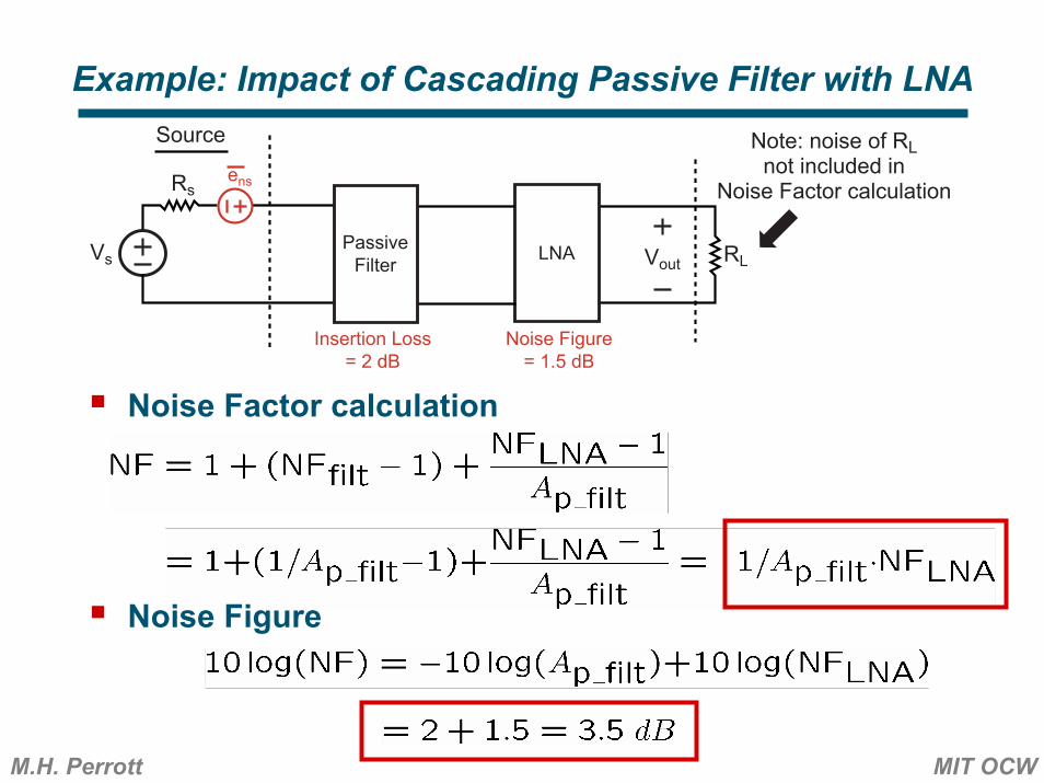
Example: Impact of Cascading Passive Filter with LNA
Vout RL
Rsens
Source
Vs
Note: noise of RLnot included in
Noise Factor calculation
PassiveFilter LNA
Insertion Loss= 2 dB
Noise Figure= 1.5 dB
Noise Factor calculation
Noise Figure
M.H. Perrott MIT OCW
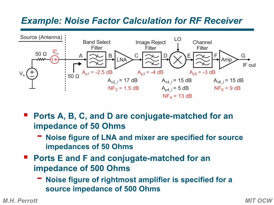
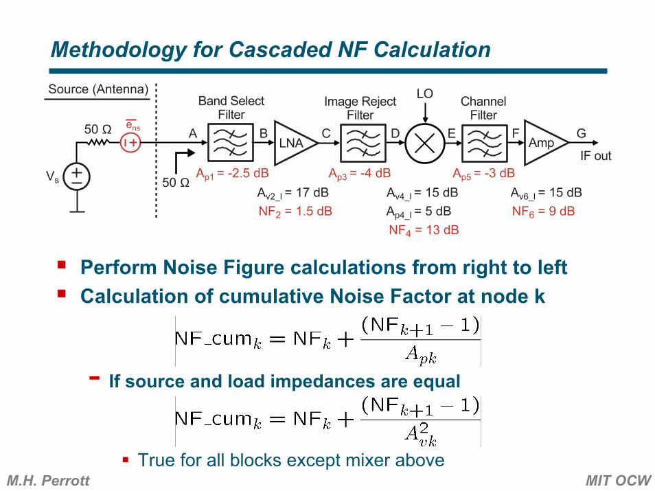
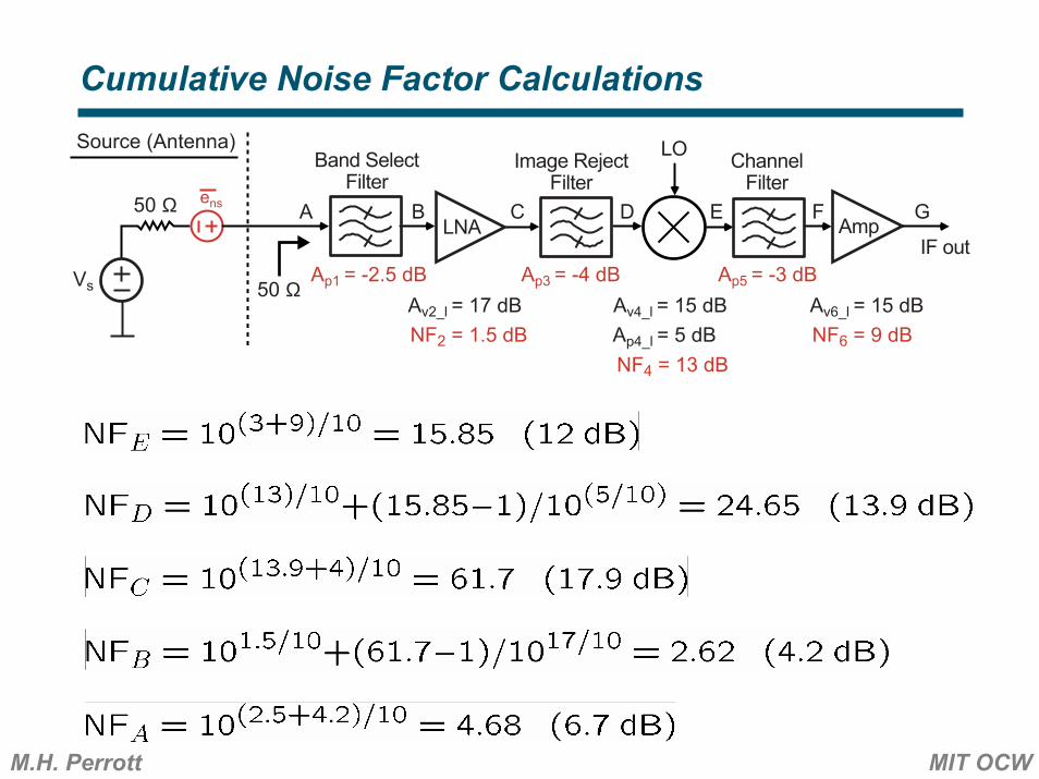
Example: Noise Factor Calculation for RF Receiver
Ports A, B, C, and D are conjugate-matched for an impedance of 50 Ohms- Noise figure of LNA and mixer are specified for source
impedances of 50 OhmsPorts E and F and conjugate-matched for an impedance of 500 Ohms- Noise figure of rightmost amplifier is specified for a
source impedance of 500 Ohms
LNA
Image RejectFilter
ChannelFilter
ens
Source (Antenna)
Vs
Amp
Band SelectFilter
IF out
LO
50 Ω
50 ΩAp1 = -2.5 dB
Av2_l = 17 dBNF2 = 1.5 dB
Ap3 = -4 dBAv4_l = 15 dB
NF4 = 13 dBAp4_l = 5 dB
Ap5 = -3 dB
NF6 = 9 dB
A B C D E F G
Av6_l = 15 dB
M.H. Perrott MIT OCW
Methodology for Cascaded NF Calculation
Perform Noise Figure calculations from right to leftCalculation of cumulative Noise Factor at node k
- If source and load impedances are equal
True for all blocks except mixer above
LNA
Image RejectFilter
ChannelFilter
ens
Source (Antenna)
Vs
Amp
Band SelectFilter
IF out
LO
50 Ω
50 ΩAp1 = -2.5 dB
Av2_l = 17 dBNF2 = 1.5 dB
Ap3 = -4 dBAv4_l = 15 dB
NF4 = 13 dBAp4_l = 5 dB
Ap5 = -3 dB
NF6 = 9 dB
A B C D E F G
Av6_l = 15 dB
M.H. Perrott MIT OCW
Cumulative Noise Factor Calculations
LNA
Image RejectFilter
ChannelFilter
ens
Source (Antenna)
Vs
Amp
Band SelectFilter
IF out
LO
50 Ω
50 ΩAp1 = -2.5 dB
Av2_l = 17 dBNF2 = 1.5 dB
Ap3 = -4 dBAv4_l = 15 dB
NF4 = 13 dBAp4_l = 5 dB
Ap5 = -3 dB
NF6 = 9 dB
A B C D E F G
Av6_l = 15 dB
M.H. Perrott MIT OCW
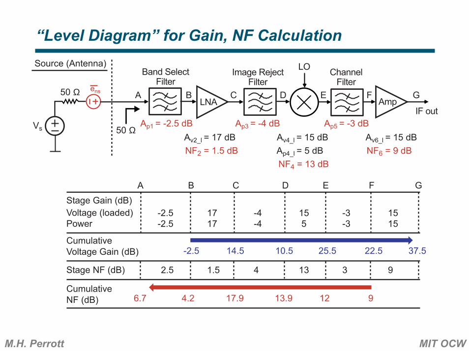
“Level Diagram” for Gain, NF Calculation
Stage Gain (dB)Voltage (loaded)Power
CumulativeVoltage Gain (dB)
Stage NF (dB)
CumulativeNF (dB)
A B C D E F G
-2.5 14.5 10.5 25.5 22.5
-2.5 17 -4 15 -3-2.5 17 -4 5 -3
1515
37.5
2.5 1.5 4 13 3 9
6.7 4.2 17.9 13.9 12 9
LNA
Image RejectFilter
ChannelFilter
ens
Source (Antenna)
Vs
Amp
Band SelectFilter
IF out
LO
50 Ω
50 ΩAp1 = -2.5 dB
Av2_l = 17 dBNF2 = 1.5 dB
Ap3 = -4 dBAv4_l = 15 dB
NF4 = 13 dBAp4_l = 5 dB
Ap5 = -3 dB
NF6 = 9 dB
A B C D E F G
Av6_l = 15 dB
M.H. Perrott MIT OCW
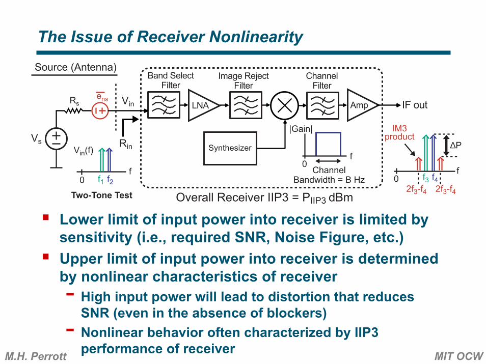
The Issue of Receiver Nonlinearity
Lower limit of input power into receiver is limited by sensitivity (i.e., required SNR, Noise Figure, etc.)Upper limit of input power into receiver is determined by nonlinear characteristics of receiver- High input power will lead to distortion that reduces
SNR (even in the absence of blockers)- Nonlinear behavior often characterized by IIP3
performance of receiver
Synthesizer
LNA
Image RejectFilter
ChannelFilter
Rsens
Source (Antenna)
Vs Rin
0Channel
Bandwidth = B Hz
f
|Gain|
Overall Receiver IIP3 = PIIP3 dBm
Amp
Band SelectFilter
IF out
f10 f2f
Vin(f)
Two-Tone Test
Vin
f0
∆P
2f3-f4 2f3-f4
IM3product
f3 f4
M.H. Perrott MIT OCW
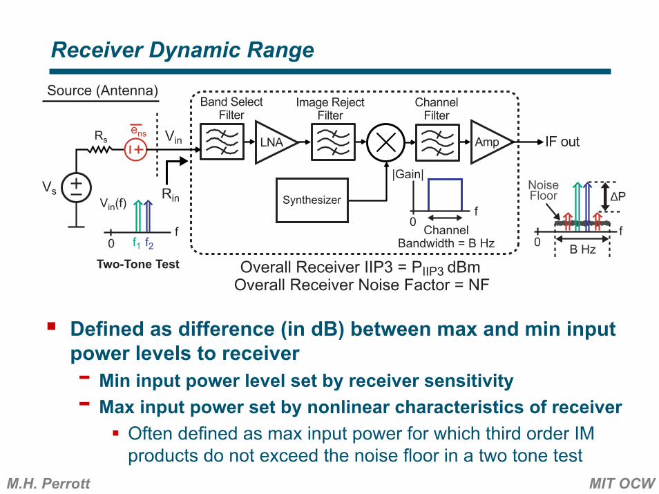
Receiver Dynamic Range
Defined as difference (in dB) between max and min input power levels to receiver- Min input power level set by receiver sensitivity- Max input power set by nonlinear characteristics of receiver
Often defined as max input power for which third order IM products do not exceed the noise floor in a two tone test
Synthesizer
LNA
Image RejectFilter
ChannelFilter
Rsens
Source (Antenna)
Vs Rin
0Channel
Bandwidth = B Hz
f
|Gain|
Overall Receiver IIP3 = PIIP3 dBm
Amp
Band SelectFilter
IF out
f10 f2f
Vin(f)
Two-Tone Test
Vin
f0
NoiseFloor ∆P
B Hz
Overall Receiver Noise Factor = NF
M.H. Perrott MIT OCW
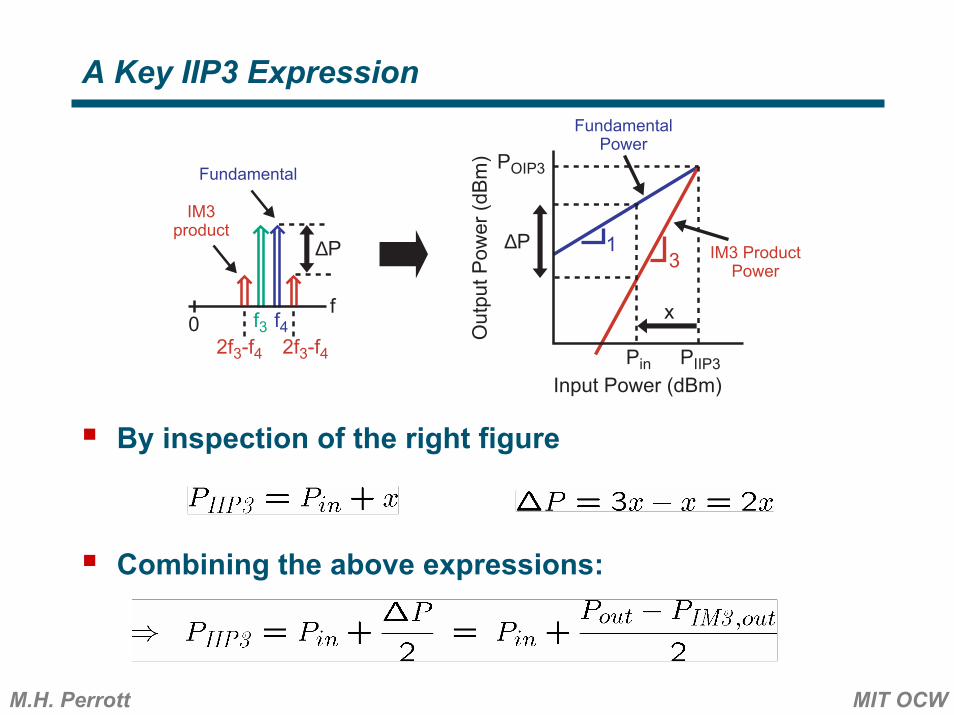
A Key IIP3 Expression
By inspection of the right figure
Combining the above expressions:
f0
∆P
2f3-f4 2f3-f4
IM3product
f3 f4PIIP3
POIP3
∆P
x
Pin
FundamentalPower
IM3 ProductPower
Fundamental
13
Input Power (dBm)
Out
put P
ower
(dBm
)
M.H. Perrott MIT OCW
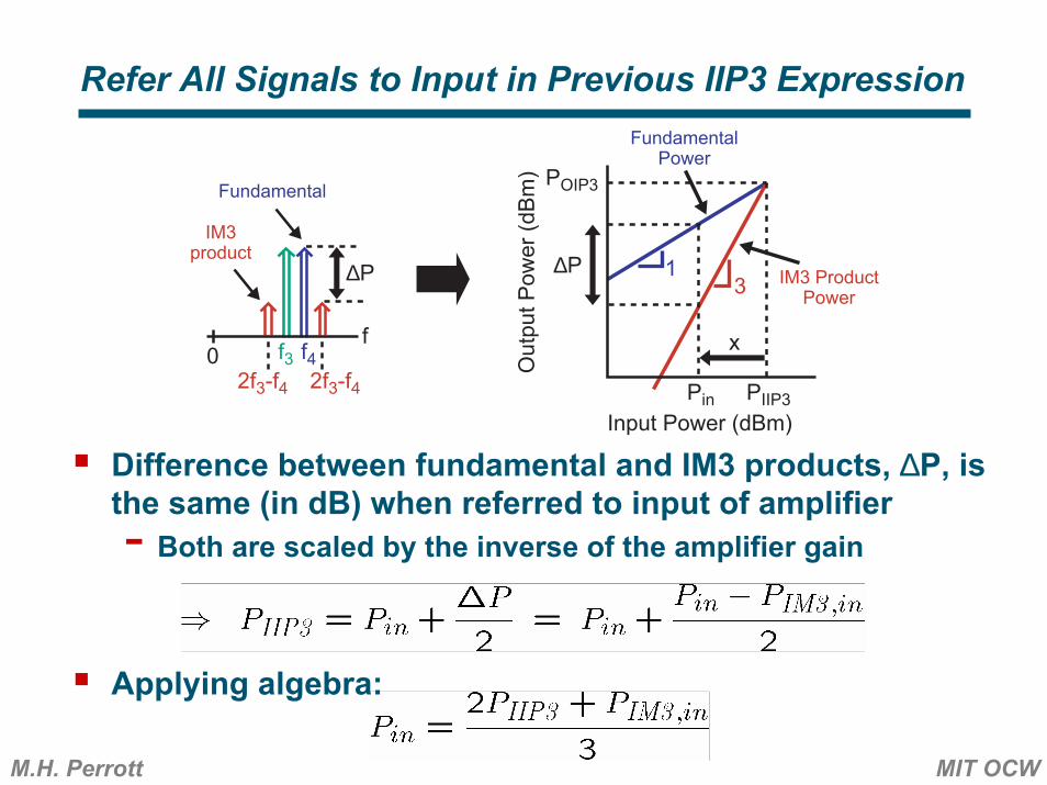
Refer All Signals to Input in Previous IIP3 Expression
Difference between fundamental and IM3 products, ∆P, is the same (in dB) when referred to input of amplifier- Both are scaled by the inverse of the amplifier gain
Applying algebra:
f0
∆P
2f3-f4 2f3-f4
IM3product
f3 f4PIIP3
POIP3
∆P
x
Pin
FundamentalPower
IM3 ProductPower
Fundamental
13
Input Power (dBm)
Out
put P
ower
(dBm
)
M.H. Perrott MIT OCW
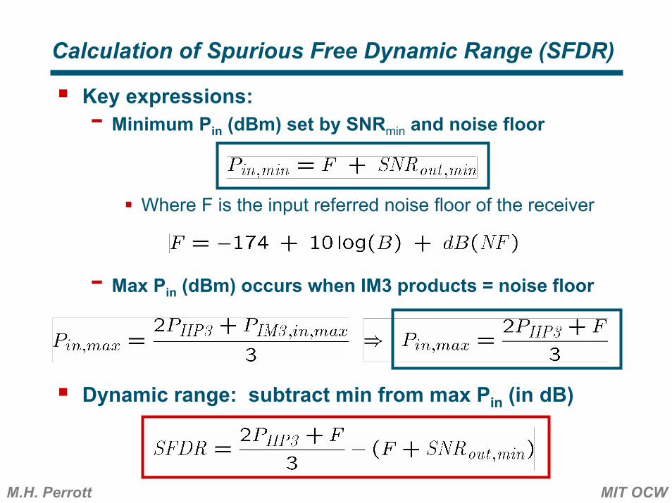
Calculation of Spurious Free Dynamic Range (SFDR)
Key expressions:- Minimum Pin (dBm) set by SNRmin and noise floor
Where F is the input referred noise floor of the receiver
- Max Pin (dBm) occurs when IM3 products = noise floor
Dynamic range: subtract min from max Pin (in dB)
M.H. Perrott MIT OCW
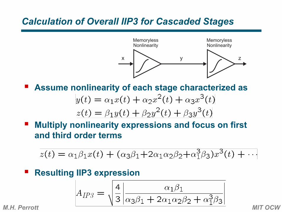
Calculation of Overall IIP3 for Cascaded Stages
Assume nonlinearity of each stage characterized as
Multiply nonlinearity expressions and focus on first and third order terms
Resulting IIP3 expression
MemorylessNonlinearity
x y
MemorylessNonlinearity
z
M.H. Perrott MIT OCW
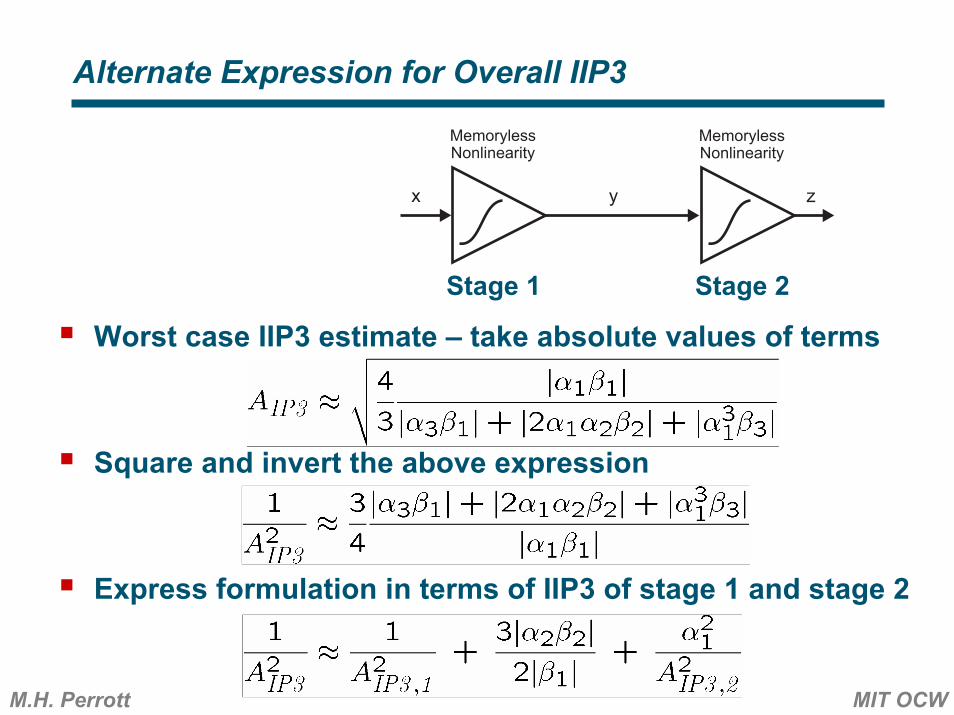
Alternate Expression for Overall IIP3
Worst case IIP3 estimate – take absolute values of terms
Square and invert the above expression
Express formulation in terms of IIP3 of stage 1 and stage 2
MemorylessNonlinearity
x y
MemorylessNonlinearity
z
Stage 1 Stage 2
M.H. Perrott MIT OCW
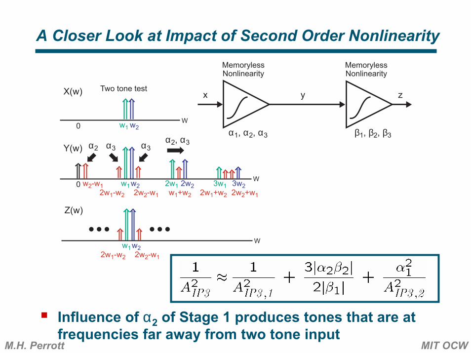
A Closer Look at Impact of Second Order Nonlinearity
Influence of α2 of Stage 1 produces tones that are at frequencies far away from two tone input
MemorylessNonlinearity
x y
w10 w2W
X(w) Two tone test
0 w12w2+w1
w2 2w22w1-w2 2w1+w22w2-w1 w1+w2
w2-w1 2w1 3w23w1W
Y(w)
MemorylessNonlinearity
z
w1w22w1-w2 2w2-w1
W
Z(w)
α2, α3α3 α3α2
α1, α2, α3 β1, β2, β3
M.H. Perrott MIT OCW
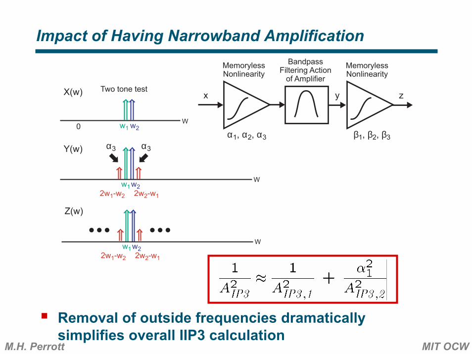
Impact of Having Narrowband Amplification
Removal of outside frequencies dramatically simplifies overall IIP3 calculation
MemorylessNonlinearity
x y
w10 w2W
X(w) Two tone test
w1w22w1-w2 2w2-w1
W
Y(w)
MemorylessNonlinearity
z
BandpassFiltering Action
of Amplifier
w1w22w1-w2 2w2-w1
W
Z(w)
α3 α3
α1, α2, α3 β1, β2, β3
M.H. Perrott MIT OCW
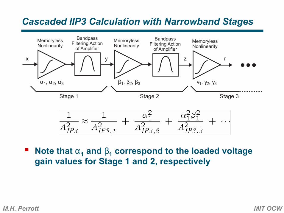
Cascaded IIP3 Calculation with Narrowband Stages
Note that α1 and β1 correspond to the loaded voltage gain values for Stage 1 and 2, respectively
MemorylessNonlinearity
x y
MemorylessNonlinearity
z
BandpassFiltering Action
of AmplifierMemorylessNonlinearity
r
BandpassFiltering Action
of Amplifier
Stage 1 Stage 2 Stage 3
α1, α2, α3 β1, β2, β3 γ1, γ2, γ3
M.H. Perrott MIT OCW
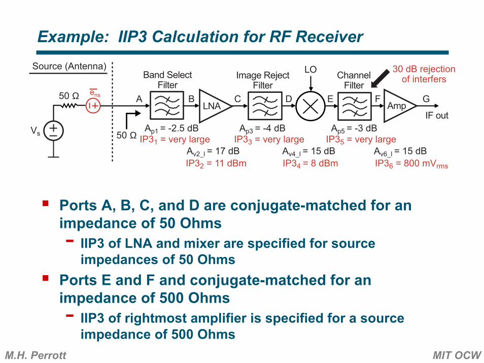
Example: IIP3 Calculation for RF Receiver
Ports A, B, C, and D are conjugate-matched for an impedance of 50 Ohms- IIP3 of LNA and mixer are specified for source
impedances of 50 OhmsPorts E and F and conjugate-matched for an impedance of 500 Ohms- IIP3 of rightmost amplifier is specified for a source
impedance of 500 Ohms
LNA
Image RejectFilter
ChannelFilter
ens
Source (Antenna)
Vs
Amp
Band SelectFilter
IF out
LO
50 Ω
50 ΩAp1 = -2.5 dB
Av2_l = 17 dBIP32 = 11 dBm
Ap3 = -4 dB
Av4_l = 15 dBIP34 = 8 dBm
Ap5 = -3 dB
IP36 = 800 mVrms
A B C D E F G
Av6_l = 15 dBIP31 = very large IP33 = very large IP35 = very large
30 dB rejectionof interfers
M.H. Perrott MIT OCW
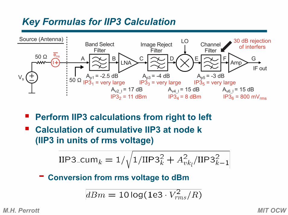
Key Formulas for IIP3 Calculation
Perform IIP3 calculations from right to leftCalculation of cumulative IIP3 at node k (IIP3 in units of rms voltage)
- Conversion from rms voltage to dBm
LNA
Image RejectFilter
ChannelFilter
ens
Source (Antenna)
Vs
Amp
Band SelectFilter
IF out
LO
50 Ω
50 ΩAp1 = -2.5 dB
Av2_l = 17 dBIP32 = 11 dBm
Ap3 = -4 dB
Av4_l = 15 dBIP34 = 8 dBm
Ap5 = -3 dB
IP36 = 800 mVrms
A B C D E F G
Av6_l = 15 dBIP31 = very large IP33 = very large IP35 = very large
30 dB rejectionof interfers
M.H. Perrott MIT OCW
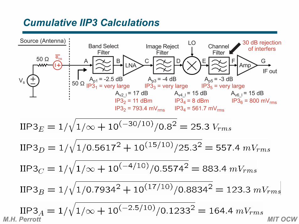
Cumulative IIP3 Calculations
LNA
Image RejectFilter
ChannelFilter
ens
Source (Antenna)
Vs
Amp
Band SelectFilter
IF out
LO
50 Ω
50 ΩAp1 = -2.5 dB
Av2_l = 17 dBIP32 = 11 dBm
Ap3 = -4 dB
Av4_l = 15 dBIP34 = 8 dBm
Ap5 = -3 dB
IP36 = 800 mVrms
A B C D E F G
Av6_l = 15 dBIP31 = very large IP33 = very large IP35 = very large
30 dB rejectionof interfers
IP32 = 793.4 mVrms IP34 = 561.7 mVrms
M.H. Perrott MIT OCW
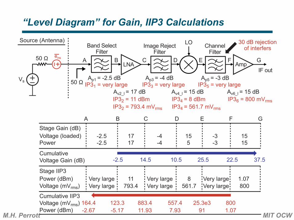
“Level Diagram” for Gain, IIP3 Calculations
Stage Gain (dB)Voltage (loaded)Power
CumulativeVoltage Gain (dB)
Stage IIP3
Cumulative IIP3Voltage (mVrms)
A B C D E F G
-2.5 14.5 10.5 25.5 22.5
-2.5 17 -4 15 -3-2.5 17 -4 5 -3
1515
37.5
Very large 11 Very large 8 Very large 1.07
164.4 123.3 883.4 557.4 25.3e3 800
LNA
Image RejectFilter
ChannelFilter
ens
Source (Antenna)
Vs
Amp
Band SelectFilter
IF out
LO
50 Ω
50 ΩAp1 = -2.5 dB
Av2_l = 17 dBIP32 = 11 dBm
Ap3 = -4 dB
Av4_l = 15 dBIP34 = 8 dBm
Ap5 = -3 dB
IP36 = 800 mVrms
A B C D E F G
Av6_l = 15 dBIP31 = very large IP33 = very large IP35 = very large
Voltage (mVrms)Power (dBm)
Very large 793.4 Very large 561.7 Very large 800
30 dB rejectionof interfers
-2.67 -5.17 11.93 7.93 91 1.07Power (dBm)
IP32 = 793.4 mVrms IP34 = 561.7 mVrms
M.H. Perrott MIT OCW
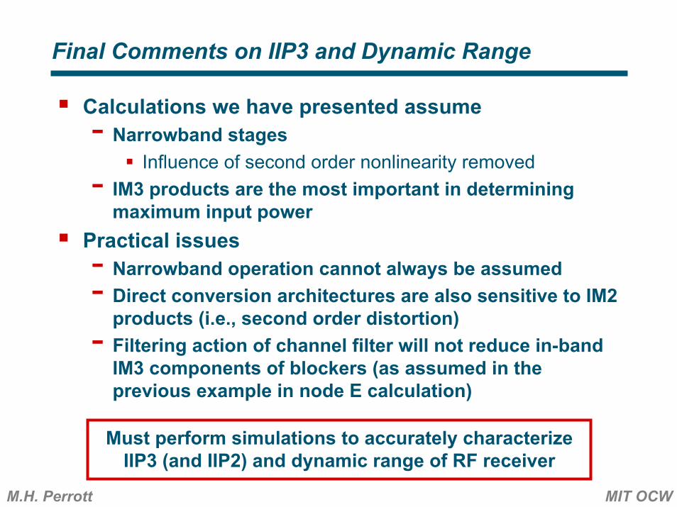
Final Comments on IIP3 and Dynamic Range
Calculations we have presented assume- Narrowband stages
Influence of second order nonlinearity removed- IM3 products are the most important in determining
maximum input powerPractical issues- Narrowband operation cannot always be assumed- Direct conversion architectures are also sensitive to IM2
products (i.e., second order distortion)- Filtering action of channel filter will not reduce in-band
IM3 components of blockers (as assumed in the previous example in node E calculation)
Must perform simulations to accurately characterizeIIP3 (and IIP2) and dynamic range of RF receiver