4 x 41 W quad bridge car radio amplifier -...
11
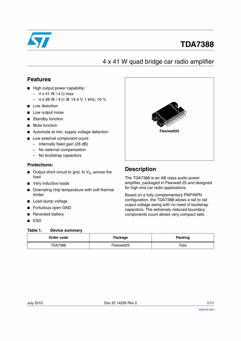
July 2010 Doc ID 14256 Rev 2 1/11 1 TDA7388 4 x 41 W quad bridge car radio amplifier Features ■ High output power capability: – 4 x 41 W / 4 Ω max. – 4 x 26 W / 4 Ω @ 14.4 V, 1 kHz, 10 % ■ Low distortion ■ Low output noise ■ Standby function ■ Mute function ■ Automute at min. supply voltage detection ■ Low external component count: – Internally fixed gain (26 dB) – No external compensation – No bootstrap capacitors Protections: ■ Output short circuit to gnd, to V S , across the load ■ Very inductive loads ■ Overrating chip temperature with soft thermal limiter ■ Load dump voltage ■ Fortuitous open GND ■ Reversed battery ■ ESD Description The TDA7388 is an AB class audio power amplifier, packaged in Flexiwatt 25 and designed for high end car radio applications. Based on a fully complementary PNP/NPN configuration, the TDA7388 allows a rail to rail output voltage swing with no need of bootstrap capacitors. The extremely reduced boundary components count allows very compact sets. Flexiwatt25 Table 1. Device summary Order code Package Packing TDA7388 Flexiwatt25 Tube www.st.com
Transcript of 4 x 41 W quad bridge car radio amplifier -...
July 2010 Doc ID 14256 Rev 2 1/11
1
TDA7388
4 x 41 W quad bridge car radio amplifier
Features■ High output power capability:
– 4 x 41 W / 4 Ω max.– 4 x 26 W / 4 Ω @ 14.4 V, 1 kHz, 10 %
■ Low distortion
■ Low output noise
■ Standby function
■ Mute function
■ Automute at min. supply voltage detection
■ Low external component count:– Internally fixed gain (26 dB)– No external compensation– No bootstrap capacitors
Protections:
■ Output short circuit to gnd, to VS, across the load
■ Very inductive loads
■ Overrating chip temperature with soft thermal limiter
■ Load dump voltage
■ Fortuitous open GND
■ Reversed battery
■ ESD
DescriptionThe TDA7388 is an AB class audio power amplifier, packaged in Flexiwatt 25 and designed for high end car radio applications.
Based on a fully complementary PNP/NPN configuration, the TDA7388 allows a rail to rail output voltage swing with no need of bootstrap capacitors. The extremely reduced boundary components count allows very compact sets.
Flexiwatt25
Table 1. Device summary
Order code Package Packing
TDA7388 Flexiwatt25 Tube
www.st.com
Contents TDA7388
2/11 Doc ID 14256 Rev 2
Contents
1 Pin connection and test/application diagrams . . . . . . . . . . . . . . . . . . . . 5
2 Electrical specifications . . . . . . . . . . . . . . . . . . . . . . . . . . . . . . . . . . . . . . 6
2.1 Absolute maximum ratings . . . . . . . . . . . . . . . . . . . . . . . . . . . . . . . . . . . . . 6
2.2 Thermal data . . . . . . . . . . . . . . . . . . . . . . . . . . . . . . . . . . . . . . . . . . . . . . . 6
2.3 Electrical characteristics . . . . . . . . . . . . . . . . . . . . . . . . . . . . . . . . . . . . . . . 6
3 Application hints . . . . . . . . . . . . . . . . . . . . . . . . . . . . . . . . . . . . . . . . . . . . 8
3.1 SVR . . . . . . . . . . . . . . . . . . . . . . . . . . . . . . . . . . . . . . . . . . . . . . . . . . . . . . 8
3.2 Input stage . . . . . . . . . . . . . . . . . . . . . . . . . . . . . . . . . . . . . . . . . . . . . . . . . 8
3.3 Standby and muting . . . . . . . . . . . . . . . . . . . . . . . . . . . . . . . . . . . . . . . . . . 8
4 Package information . . . . . . . . . . . . . . . . . . . . . . . . . . . . . . . . . . . . . . . . . 9
5 Revision history . . . . . . . . . . . . . . . . . . . . . . . . . . . . . . . . . . . . . . . . . . . 10
TDA7388 List of tables
Doc ID 14256 Rev 2 3/11
List of tables
Table 1. Device summary . . . . . . . . . . . . . . . . . . . . . . . . . . . . . . . . . . . . . . . . . . . . . . . . . . . . . . . . . . 1Table 2. Absolute maximum ratings . . . . . . . . . . . . . . . . . . . . . . . . . . . . . . . . . . . . . . . . . . . . . . . . . . 6Table 3. Thermal data. . . . . . . . . . . . . . . . . . . . . . . . . . . . . . . . . . . . . . . . . . . . . . . . . . . . . . . . . . . . . 6Table 4. Electrical characteristics . . . . . . . . . . . . . . . . . . . . . . . . . . . . . . . . . . . . . . . . . . . . . . . . . . . . 6Table 5. Document revision history . . . . . . . . . . . . . . . . . . . . . . . . . . . . . . . . . . . . . . . . . . . . . . . . . 10
List of figures TDA7388
4/11 Doc ID 14256 Rev 2
List of figures
Figure 1. Pin connection (top view) . . . . . . . . . . . . . . . . . . . . . . . . . . . . . . . . . . . . . . . . . . . . . . . . . . . 5Figure 2. Standard test and application circuit . . . . . . . . . . . . . . . . . . . . . . . . . . . . . . . . . . . . . . . . . . . 5Figure 3. Flexiwatt25 mechanical data and package dimensions . . . . . . . . . . . . . . . . . . . . . . . . . . . . 9
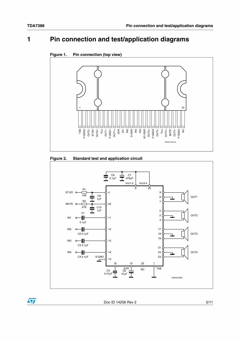
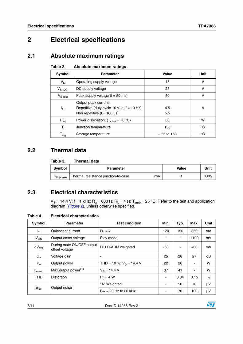
TDA7388 Pin connection and test/application diagrams
Doc ID 14256 Rev 2 5/11
1 Pin connection and test/application diagrams
Figure 1. Pin connection (top view)
Figure 2. Standard test and application circuit
D94AU159mod
TA
B
P-G
ND
2
OU
T2-
ST
-BY
OU
T2+
VC
C
OU
T1-
P-G
ND
1
OU
T1+
SV
R
IN1
IN2
S-G
ND
IN4
IN3
AC
-GN
D
OU
T3+
P-G
ND
3
OU
T3-
VC
C
OU
T4+
MU
TE
OU
T4-
P-G
ND
4
NC
1 25
IN1
0.1μF
C91μF
IN2
C2 0.1μF
OUT1
OUT2
IN3
C3 0.1μF
IN4
C4 0.1μF
OUT3
OUT4
D95AU335E
C50.47μF
C647μF
SVR TAB
Vcc1-2 Vcc3-4
C80.1μF
C7470μF
C101μF
ST-BYR1
10K
R2
47KMUTE
C1
14
15
12
11
22
4
13S-GND
16 10 25 1
NC
6 20
9
8
7
5
2
3
17
18
19
21
24
23
Electrical specifications TDA7388
6/11 Doc ID 14256 Rev 2
2 Electrical specifications
2.1 Absolute maximum ratings
2.2 Thermal data
2.3 Electrical characteristicsVS = 14.4 V; f = 1 kHz; Rg = 600 Ω; RL = 4 Ω; Tamb = 25 °C; Refer to the test and application diagram (Figure 2), unless otherwise specified.
Table 2. Absolute maximum ratings
Symbol Parameter Value Unit
VS Operating supply voltage 18 V
VS (DC) DC supply voltage 28 V
VS (pk) Peak supply voltage (t = 50 ms) 50 V
IO
Output peak current:Repetitive (duty cycle 10 % at f = 10 Hz)
Non repetitive (t = 100 µs)
4.5
5.5
A
Ptot Power dissipation, (Tcase = 70 °C) 80 W
Tj Junction temperature 150 °C
Tstg Storage temperature – 55 to 150 °C
Table 3. Thermal data
Symbol Parameter Value Unit
Rth j-case Thermal resistance junction-to-case max. 1 °C/W
Table 4. Electrical characteristics
Symbol Parameter Test condition Min. Typ. Max. Unit
Iq1 Quiescent current RL = ∞ 120 190 350 mA
VOS Output offset voltage Play mode - - ±100 mV
dVOSDuring mute ON/OFF output offset voltage
ITU R-ARM weighted -80 - +80 mV
Gv Voltage gain - 25 26 27 dB
Po Output power THD = 10 %; VS = 14.4 V 22 26 - W
Po max Max.output power(1) VS = 14.4 V 37 41 - W
THD Distortion Po = 4 W - 0.04 0.15 %
eNo Output noise"A" Weighted - 50 70 µV
Bw = 20 Hz to 20 kHz - 70 100 µV
TDA7388 Electrical specifications
Doc ID 14256 Rev 2 7/11
SVR Supply voltage rejection f = 100 Hz; Vr = 1 Vrms 50 65 - dB
fch High cut-off frequency Po = 0.5 W 100 200 - KHz
Ri Input Impedance - 70 100 - KΩ
CT Cross talkf = 1 kHz; Po = 4 W 60 70 - dB
f = 10 kHz; Po = 4 W - 60 - dB
ISBStandby current consumption
VSt-by = 0V - - 20 µA
VSB outStandby OUT threshold voltage
(Amp: ON) 3.5 - - V
VSB INStandby IN threshold voltage
(Amp: OFF) - - 1.5 V
AM Mute attenuation POref = 4 W 80 90 - dB
VM out Mute OUT threshold voltage (Amp: play) 3.5 - - V
VM in Mute IN threshold voltage (Amp: mute) - - 1.5 V
VAM in VS automute threshold
(Amp: mute); Att. ≥ 80 dB;
POref = 4 W
(Amp: play); Att. < 0.1 dB;PO = 0.5 W
-
7.6
6.5
8.5
V
Ipin22 Muting pin current VMUTE = 1.2 V (Source current) 5 11 20 µA
1. Saturated square wave output.
Table 4. Electrical characteristics (continued)
Symbol Parameter Test condition Min. Typ. Max. Unit
Application hints TDA7388
8/11 Doc ID 14256 Rev 2
3 Application hints
Ref. to the circuit of Figure 2.
3.1 SVRBesides its contribution to the ripple rejection, the SVR capacitor governs the turn ON/OFF time sequence and, consequently, plays an essential role in the pop optimization during ON/OFF transients.
To conveniently serve both needs, its minimum recommended value is 10 µF.
3.2 Input stageThe TDA7388’s inputs are ground-compatible and can stand very high input signals(±8 Vpk) without any performances degradation.
If the standard value for the input capacitors (0.1 µF) is adopted, the low frequency cut-off amounts to 16 Hz.
3.3 Standby and mutingStandby and Muting facilities are both 3.3 V CMOS-compatible. If unused, a straight connection to Vs of their respective pins would be admissible.
Conventional/low-power transistors can be employed to drive muting and standby pins in absence of true CMOS ports or microprocessors. R-C cells have always to be used in order to smooth down the transitions for preventing any audible transient noises.
Since a DC current of about 10 µA normally flows out of pin 22, the maximum allowable muting-series resistance (R2) is 70 kΩ, which is sufficiently high to permit a muting capacitor reasonably small (about 1 µF).
If R2 is higher than recommended, the involved risk is that the voltage at pin 22 may rises to above the 1.5 V threshold voltage and the device consequently fails to turn OFF when the mute line is brought down.
About the stand-by, the time constant to be assigned in order to obtain a virtually pop-free transition has to be slower than 2.5 V/ms.
TDA7388 Package information
Doc ID 14256 Rev 2 9/11
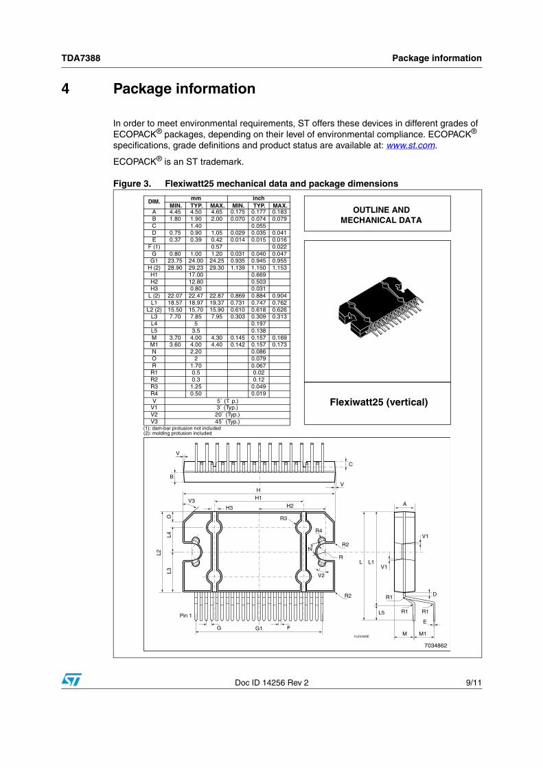
4 Package information
In order to meet environmental requirements, ST offers these devices in different grades of ECOPACK® packages, depending on their level of environmental compliance. ECOPACK®
specifications, grade definitions and product status are available at: www.st.com.
ECOPACK® is an ST trademark.
Figure 3. Flexiwatt25 mechanical data and package dimensions
OUTLINE ANDMECHANICAL DATA
DIM. mm inchMIN. TYP. MAX. MIN. TYP. MAX.
A 4.45 4.50 4.65 0.175 0.177 0.183B 1.80 1.90 2.00 0.070 0.074 0.079C 1.40 0.055D 0.75 0.90 1.05 0.029 0.035 0.041E 0.37 0.39 0.42 0.014 0.015 0.016
F (1) 0.57 0.022G 0.80 1.00 1.20 0.031 0.040 0.047G1 23.75 24.00 24.25 0.935 0.945 0.955
H (2) 28.90 29.23 29.30 1.139 1.150 1.153H1 17.00 0.669H2 12.80 0.503H3 0.80 0.031
L (2) 22.07 22.47 22.87 0.869 0.884 0.904L1 18.57 18.97 19.37 0.731 0.747 0.762
L2 (2) 15.50 15.70 15.90 0.610 0.618 0.626L3 7.70 7.85 7.95 0.303 0.309 0.313L4 5 0.197L5 3.5 0.138M 3.70 4.00 4.30 0.145 0.157 0.169M1 3.60 4.00 4.40 0.142 0.157 0.173N 2.20 0.086O 2 0.079R 1.70 0.067R1 0.5 0.02R2 0.3 0.12R3 1.25 0.049R4 0.50 0.019
V1 3˚ (Typ.)V 5˚ (T p.)
V2 20˚ (Typ.)V3 45˚ (Typ.)
(2): molding protusion included(1): dam-bar protusion not included
Flexiwatt25 (vertical)
H3
R4
G
V
G1
L2
H1H
FM1
L
FLEX25ME
V3
OL3
L4
H2
R3
N
V2
R
R2
R2
C
B
L1
M
R1
L5 R1 R1
E
D
A
Pin 1
V
V1
V1
7034862
Revision history TDA7388
10/11 Doc ID 14256 Rev 2
5 Revision history
Table 5. Document revision history
Date Revision Changes
06-Dec-2007 1 Initial release.
12-Jul-2010 2 Document status promoted from preliminary data to datasheet.
TDA7388
Doc ID 14256 Rev 2 11/11
Please Read Carefully:
Information in this document is provided solely in connection with ST products. STMicroelectronics NV and its subsidiaries (“ST”) reserve theright to make changes, corrections, modifications or improvements, to this document, and the products and services described herein at anytime, without notice.
All ST products are sold pursuant to ST’s terms and conditions of sale.
Purchasers are solely responsible for the choice, selection and use of the ST products and services described herein, and ST assumes noliability whatsoever relating to the choice, selection or use of the ST products and services described herein.
No license, express or implied, by estoppel or otherwise, to any intellectual property rights is granted under this document. If any part of thisdocument refers to any third party products or services it shall not be deemed a license grant by ST for the use of such third party productsor services, or any intellectual property contained therein or considered as a warranty covering the use in any manner whatsoever of suchthird party products or services or any intellectual property contained therein.
UNLESS OTHERWISE SET FORTH IN ST’S TERMS AND CONDITIONS OF SALE ST DISCLAIMS ANY EXPRESS OR IMPLIEDWARRANTY WITH RESPECT TO THE USE AND/OR SALE OF ST PRODUCTS INCLUDING WITHOUT LIMITATION IMPLIEDWARRANTIES OF MERCHANTABILITY, FITNESS FOR A PARTICULAR PURPOSE (AND THEIR EQUIVALENTS UNDER THE LAWSOF ANY JURISDICTION), OR INFRINGEMENT OF ANY PATENT, COPYRIGHT OR OTHER INTELLECTUAL PROPERTY RIGHT.
UNLESS EXPRESSLY APPROVED IN WRITING BY AN AUTHORIZED ST REPRESENTATIVE, ST PRODUCTS ARE NOTRECOMMENDED, AUTHORIZED OR WARRANTED FOR USE IN MILITARY, AIR CRAFT, SPACE, LIFE SAVING, OR LIFE SUSTAININGAPPLICATIONS, NOR IN PRODUCTS OR SYSTEMS WHERE FAILURE OR MALFUNCTION MAY RESULT IN PERSONAL INJURY,DEATH, OR SEVERE PROPERTY OR ENVIRONMENTAL DAMAGE. ST PRODUCTS WHICH ARE NOT SPECIFIED AS "AUTOMOTIVEGRADE" MAY ONLY BE USED IN AUTOMOTIVE APPLICATIONS AT USER’S OWN RISK.
Resale of ST products with provisions different from the statements and/or technical features set forth in this document shall immediately voidany warranty granted by ST for the ST product or service described herein and shall not create or extend in any manner whatsoever, anyliability of ST.
ST and the ST logo are trademarks or registered trademarks of ST in various countries.
Information in this document supersedes and replaces all information previously supplied.
The ST logo is a registered trademark of STMicroelectronics. All other names are the property of their respective owners.
© 2010 STMicroelectronics - All rights reserved
STMicroelectronics group of companies
Australia - Belgium - Brazil - Canada - China - Czech Republic - Finland - France - Germany - Hong Kong - India - Israel - Italy - Japan - Malaysia - Malta - Morocco - Philippines - Singapore - Spain - Sweden - Switzerland - United Kingdom - United States of America
www.st.com