![Playing with Protons - ΕΚΦΕ ΧανίωνPLAYING WITH PROTONS UK CPD COURSE Hosted by Supported by 2nd Pilot CPD [Greece 2017] 2nd Pilot CPD [Greece 2017] Footprint 3,500 students](https://static.fdocument.org/doc/165x107/609f4cf37f416d44cb28e222/playing-with-protons-playing-with-protons-uk-cpd-course.jpg)
3-Axis Digital Compass IC...
20
3-Axis Digital Compass IC HMC5883L The Honeywell HMC5883L is a surface-mount, multi-chip module designed for low-field magnetic sensing with a digital interface for applications such as low- cost compassing and magnetometry. The HMC5883L includes our state-of-the- art, high-resolution HMC118X series magneto-resistive sensors plus an ASIC containing amplification, automatic degaussing strap drivers, offset cancellation, and a 12-bit ADC that enables 1° to 2° compass heading accuracy. The I 2 C serial bus allows for easy interface. The HMC5883L is a 3.0x3.0x0.9mm surface mount 16-pin leadless chip carrier (LCC). Applications for the HMC5883L include Mobile Phones, Netbooks, Consumer Electronics, Auto Navigation Systems, and Personal Navigation Devices. The HMC5883L utilizes Honeywell’s Anisotropic Magnetoresistive (AMR) technology that provides advantages over other magnetic sensor technologies. These anisotropic, directional sensors feature precision in-axis sensitivity and linearity. These sensors’ solid-state construction with very low cross-axis sensitivity is designed to measure both the direction and the magnitude of Earth’s magnetic fields, from milli-gauss to 8 gauss. Honeywell’s Magnetic Sensors are among the most sensitive and reliable low-field sensors in the industry. FEATURES BENEFITS 3-Axis Magnetoresistive Sensors and ASIC in a 3.0x3.0x0.9mm LCC Surface Mount Package Small Size for Highly Integrated Products. Just Add a Micro- Controller Interface, Plus Two External SMT Capacitors Designed for High Volume, Cost Sensitive OEM Designs Easy to Assemble & Compatible with High Speed SMT Assembly 12-Bit ADC Coupled with Low Noise AMR Sensors Achieves 2 milli-gauss Field Resolution in ±8 Gauss Fields Enables 1° to 2° Degree Compass Heading Accuracy Built-In Self Test Enables Low-Cost Functionality Test after Assembly in Production Low Voltage Operations (2.16 to 3.6V) and Low Power Consumption (100 μA) Compatible for Battery Powered Applications Built-In Strap Drive Circuits Set/Reset and Offset Strap Drivers for Degaussing, Self Test, and Offset Compensation I 2 C Digital Interface Popular Two-Wire Serial Data Interface for Consumer Electronics Lead Free Package Construction RoHS Compliance Wide Magnetic Field Range (+/-8 Oe) Sensors Can Be Used in Strong Magnetic Field Environments with a 1° to 2° Degree Compass Heading Accuracy Software and Algorithm Support Available Compassing Heading, Hard Iron, Soft Iron, and Auto Calibration Libraries Available Fast 160 Hz Maximum Output Rate Enables Pedestrian Navigation and LBS Applications Advanced Information
Transcript of 3-Axis Digital Compass IC...
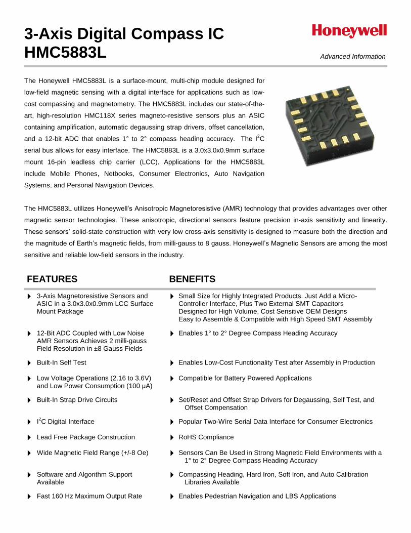
3-Axis Digital Compass IC HMC5883L
The Honeywell HMC5883L is a surface-mount, multi-chip module designed for
low-field magnetic sensing with a digital interface for applications such as low-
cost compassing and magnetometry. The HMC5883L includes our state-of-the-
art, high-resolution HMC118X series magneto-resistive sensors plus an ASIC
containing amplification, automatic degaussing strap drivers, offset cancellation,
and a 12-bit ADC that enables 1° to 2° compass heading accuracy. The I2C
serial bus allows for easy interface. The HMC5883L is a 3.0x3.0x0.9mm surface
mount 16-pin leadless chip carrier (LCC). Applications for the HMC5883L
include Mobile Phones, Netbooks, Consumer Electronics, Auto Navigation
Systems, and Personal Navigation Devices.
The HMC5883L utilizes Honeywell’s Anisotropic Magnetoresistive (AMR) technology that provides advantages over other
magnetic sensor technologies. These anisotropic, directional sensors feature precision in-axis sensitivity and linearity.
These sensors’ solid-state construction with very low cross-axis sensitivity is designed to measure both the direction and
the magnitude of Earth’s magnetic fields, from milli-gauss to 8 gauss. Honeywell’s Magnetic Sensors are among the most
sensitive and reliable low-field sensors in the industry.
FEATURES BENEFITS
3-Axis Magnetoresistive Sensors and ASIC in a 3.0x3.0x0.9mm LCC Surface Mount Package
Small Size for Highly Integrated Products. Just Add a Micro- Controller Interface, Plus Two External SMT Capacitors Designed for High Volume, Cost Sensitive OEM Designs Easy to Assemble & Compatible with High Speed SMT Assembly
12-Bit ADC Coupled with Low Noise AMR Sensors Achieves 2 milli-gauss Field Resolution in ±8 Gauss Fields
Enables 1° to 2° Degree Compass Heading Accuracy
Built-In Self Test Enables Low-Cost Functionality Test after Assembly in Production
Low Voltage Operations (2.16 to 3.6V) and Low Power Consumption (100 μA)
Compatible for Battery Powered Applications
Built-In Strap Drive Circuits Set/Reset and Offset Strap Drivers for Degaussing, Self Test, and Offset Compensation
I2C Digital Interface
Popular Two-Wire Serial Data Interface for Consumer Electronics
Lead Free Package Construction
RoHS Compliance
Wide Magnetic Field Range (+/-8 Oe)
Sensors Can Be Used in Strong Magnetic Field Environments with a 1° to 2° Degree Compass Heading Accuracy
Software and Algorithm Support Available
Compassing Heading, Hard Iron, Soft Iron, and Auto Calibration
Libraries Available
Fast 160 Hz Maximum Output Rate Enables Pedestrian Navigation and LBS Applications
Advanced Information
HMC5883L
2 www.honeywell.com
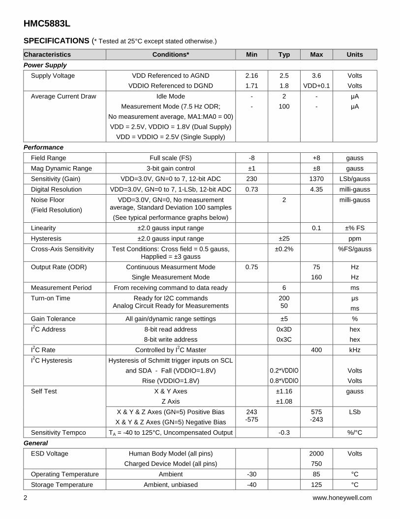
SPECIFICATIONS (* Tested at 25°C except stated otherwise.)
Characteristics Conditions* Min Typ Max Units
Power Supply
Supply Voltage VDD Referenced to AGND
VDDIO Referenced to DGND
2.16
1.71
2.5
1.8
3.6
VDD+0.1
Volts
Volts
Average Current Draw Idle Mode
Measurement Mode (7.5 Hz ODR;
No measurement average, MA1:MA0 = 00)
VDD = 2.5V, VDDIO = 1.8V (Dual Supply)
VDD = VDDIO = 2.5V (Single Supply)
-
-
2
100
-
-
μA
μA
Performance
Field Range Full scale (FS) -8 +8 gauss
Mag Dynamic Range 3-bit gain control ±1 ±8 gauss
Sensitivity (Gain) VDD=3.0V, GN=0 to 7, 12-bit ADC 230 1370 LSb/gauss
Digital Resolution VDD=3.0V, GN=0 to 7, 1-LSb, 12-bit ADC 0.73 4.35 milli-gauss
Noise Floor
(Field Resolution)
VDD=3.0V, GN=0, No measurement average, Standard Deviation 100 samples
(See typical performance graphs below)
2 milli-gauss
Linearity ±2.0 gauss input range 0.1 ±% FS
Hysteresis ±2.0 gauss input range ±25 ppm
Cross-Axis Sensitivity Test Conditions: Cross field = 0.5 gauss, Happlied = ±3 gauss
±0.2% %FS/gauss
Output Rate (ODR) Continuous Measurment Mode
Single Measurement Mode
0.75 75
160
Hz
Hz
Measurement Period From receiving command to data ready 6 ms
Turn-on Time Ready for I2C commands Analog Circuit Ready for Measurements
200 50
μs
ms
Gain Tolerance All gain/dynamic range settings ±5 %
I2C Address 8-bit read address
8-bit write address
0x3D
0x3C
hex
hex
I2C Rate Controlled by I
2C Master 400 kHz
I2C Hysteresis Hysteresis of Schmitt trigger inputs on SCL
and SDA - Fall (VDDIO=1.8V)
Rise (VDDIO=1.8V)
0.2*VDDIO
0.8*VDDIO
Volts
Volts
Self Test X & Y Axes
Z Axis
±1.16
±1.08
gauss
X & Y & Z Axes (GN=5) Positive Bias
X & Y & Z Axes (GN=5) Negative Bias
243 -575
575 -243
LSb
Sensitivity Tempco TA = -40 to 125°C, Uncompensated Output -0.3 %/°C
General
ESD Voltage Human Body Model (all pins)
Charged Device Model (all pins)
2000
750
Volts
Operating Temperature Ambient -30 85 °C
Storage Temperature Ambient, unbiased -40 125 °C
HMC5883L
www.honeywell.com 3
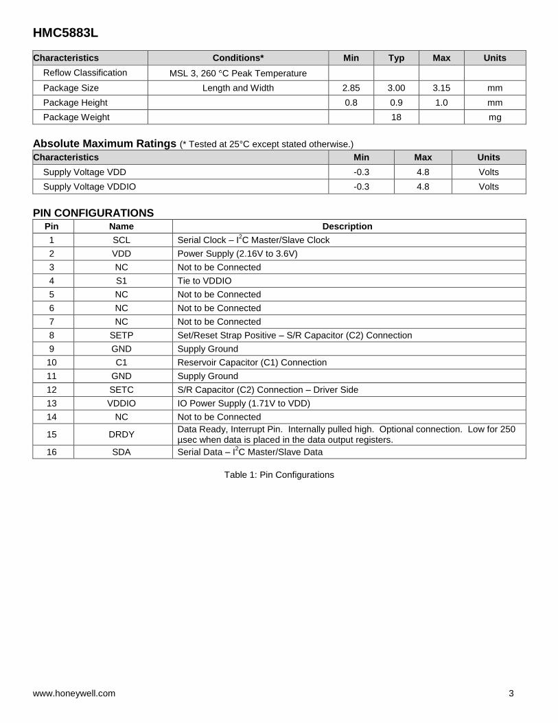
Characteristics Conditions* Min Typ Max Units
Reflow Classification MSL 3, 260 C Peak Temperature
Package Size Length and Width 2.85 3.00 3.15 mm
Package Height 0.8 0.9 1.0 mm
Package Weight 18 mg
Absolute Maximum Ratings (* Tested at 25°C except stated otherwise.)
Characteristics Min Max Units
Supply Voltage VDD -0.3 4.8 Volts
Supply Voltage VDDIO -0.3 4.8 Volts
PIN CONFIGURATIONS
Pin Name Description
1 SCL Serial Clock – I2C Master/Slave Clock
2 VDD Power Supply (2.16V to 3.6V)
3 NC Not to be Connected
4 S1 Tie to VDDIO
5 NC Not to be Connected
6 NC Not to be Connected
7 NC Not to be Connected
8 SETP Set/Reset Strap Positive – S/R Capacitor (C2) Connection
9 GND Supply Ground
10 C1 Reservoir Capacitor (C1) Connection
11 GND Supply Ground
12 SETC S/R Capacitor (C2) Connection – Driver Side
13 VDDIO IO Power Supply (1.71V to VDD)
14 NC Not to be Connected
15 DRDY Data Ready, Interrupt Pin. Internally pulled high. Optional connection. Low for 250 µsec when data is placed in the data output registers.
16 SDA Serial Data – I2C Master/Slave Data
Table 1: Pin Configurations
HMC5883L
4 www.honeywell.com
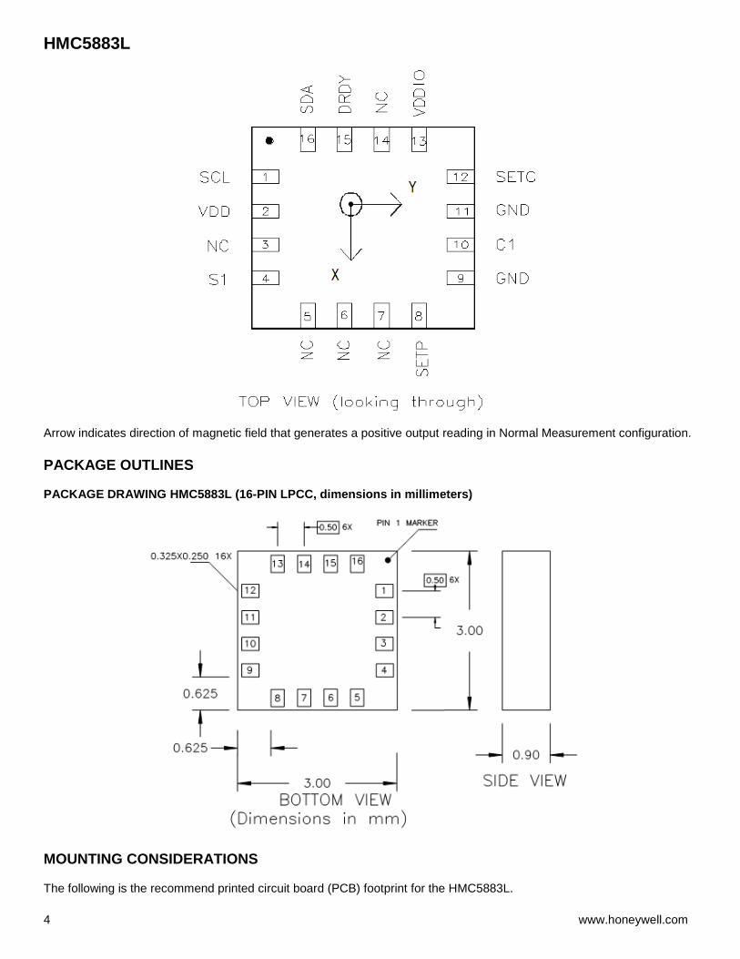
Arrow indicates direction of magnetic field that generates a positive output reading in Normal Measurement configuration.
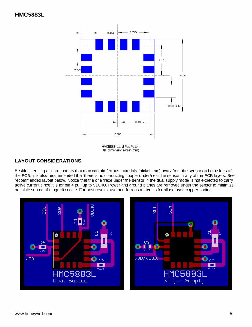
PACKAGE OUTLINES PACKAGE DRAWING HMC5883L (16-PIN LPCC, dimensions in millimeters)
MOUNTING CONSIDERATIONS The following is the recommend printed circuit board (PCB) footprint for the HMC5883L.
HMC5883L
www.honeywell.com 5
0.100
1.275
1.275
0.500
3.000
3.000
0.450
0.300
x 8
x 12
HMC5883 Land Pad Pattern(All dimensions are in mm)
LAYOUT CONSIDERATIONS Besides keeping all components that may contain ferrous materials (nickel, etc.) away from the sensor on both sides of the PCB, it is also recommended that there is no conducting copper under/near the sensor in any of the PCB layers. See recommended layout below. Notice that the one trace under the sensor in the dual supply mode is not expected to carry active current since it is for pin 4 pull-up to VDDIO. Power and ground planes are removed under the sensor to minimize possible source of magnetic noise. For best results, use non-ferrous materials for all exposed copper coding.
HMC5883L
6 www.honeywell.com
PCB Pad Definition and Traces The HMC5883L is a fine pitch LCC package. Refer to previous figure for recommended PCB footprint for proper package centering. Size the traces between the HMC5883L and the external capacitors (C1 and C2) to handle the 1 ampere peak current pulses with low voltage drop on the traces. Stencil Design and Solder Paste A 4 mil stencil and 100% paste coverage is recommended for the electrical contact pads. Reflow Assembly
This device is classified as MSL 3 with 260 C peak reflow temperature. A baking process (125 C, 24 hrs) is required if device is not kept continuously in a dry (< 10% RH) environment before assembly. No special reflow profile is required for HMC5883L, which is compatible with lead eutectic and lead-free solder paste reflow profiles. Honeywell recommends adherence to solder paste manufacturer’s guidelines. Hand soldering is not recommended. Built-in self test can be used to verify device functionalities after assembly.
External Capacitors The two external capacitors should be ceramic type construction with low ESR characteristics. The exact ESR values are not critical but values less than 200 milli-ohms are recommended. Reservoir capacitor C1 is nominally 4.7 µF in capacitance, with the set/reset capacitor C2 nominally 0.22 µF in capacitance. Low ESR characteristics may not be in many small SMT ceramic capacitors (0402), so be prepared to up-size the capacitors to gain Low ESR characteristics.
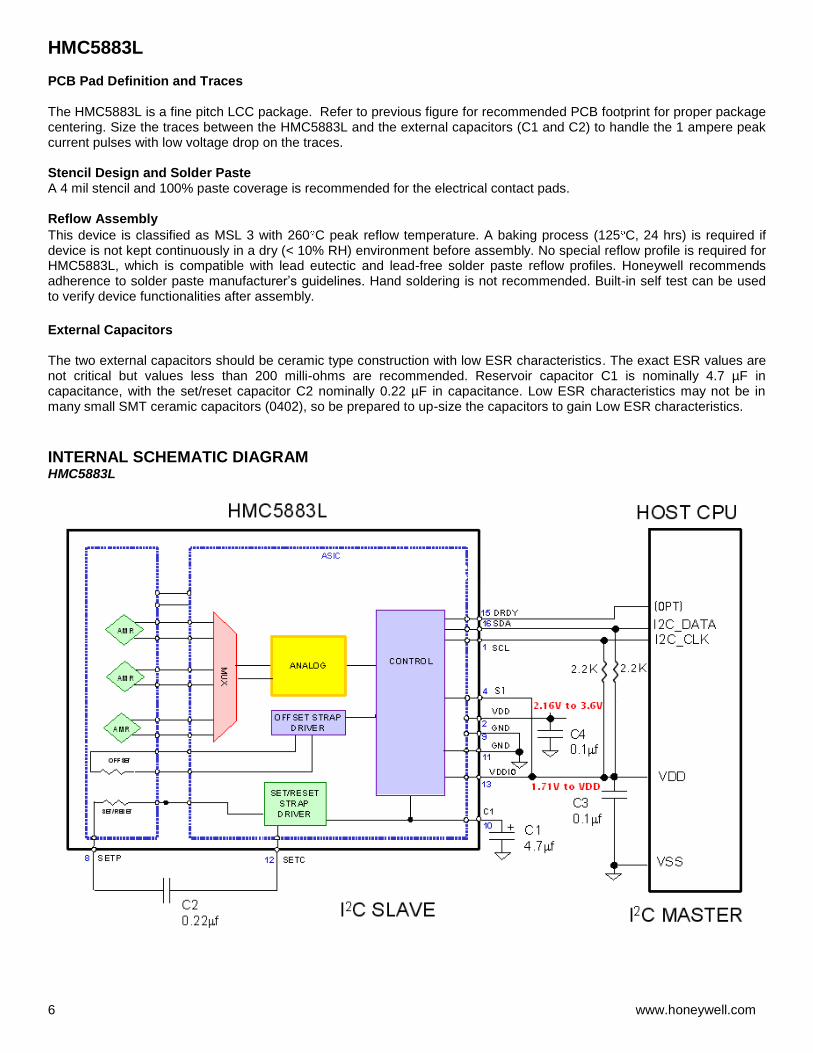
INTERNAL SCHEMATIC DIAGRAM HMC5883L
HMC5883L
www.honeywell.com 7
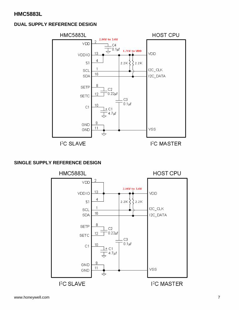
DUAL SUPPLY REFERENCE DESIGN
SINGLE SUPPLY REFERENCE DESIGN
HMC5883L
8 www.honeywell.com
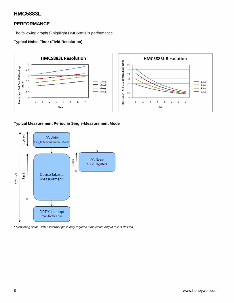
PERFORMANCE
The following graph(s) highlight HMC5883L’s performance. Typical Noise Floor (Field Resolution)
0
0.5
1
1.5
2
2.5
3
0 1 2 3 4 5 6 7Re
solu
tio
n -
Std
De
v 1
00
Re
adin
gs
(mG
a)
Gain
HMC5883L Resolution
Expon. (1)
Expon. (2)
Expon. (4)
Expon. (8)
1 Avg2 Avg4 Avg
8 Avg
Typical Measurement Period in Single-Measurement Mode
* Monitoring of the DRDY Interrupt pin is only required if maximum output rate is desired.
HMC5883L
www.honeywell.com 9
BASIC DEVICE OPERATION Anisotropic Magneto-Resistive Sensors The Honeywell HMC5883L magnetoresistive sensor circuit is a trio of sensors and application specific support circuits to measure magnetic fields. With power supply applied, the sensor converts any incident magnetic field in the sensitive axis directions to a differential voltage output. The magnetoresistive sensors are made of a nickel-iron (Permalloy) thin-film and patterned as a resistive strip element. In the presence of a magnetic field, a change in the bridge resistive elements causes a corresponding change in voltage across the bridge outputs. These resistive elements are aligned together to have a common sensitive axis (indicated by arrows in the pinout diagram) that will provide positive voltage change with magnetic fields increasing in the sensitive direction. Because the output is only proportional to the magnetic field component along its axis, additional sensor bridges are placed at orthogonal directions to permit accurate measurement of magnetic field in any orientation. Self Test To check the HMC5883L for proper operation, a self test feature in incorporated in which the sensor is internally excited with a nominal magnetic field (in either positive or negative bias configuration). This field is then measured and reported. This function is enabled and the polarity is set by bits MS[n] in the configuration register A. An internal current source generates DC current (about 10 mA) from the VDD supply. This DC current is applied to the offset straps of the magneto-resistive sensor, which creates an artificial magnetic field bias on the sensor. The difference of this measurement and the measurement of the ambient field will be put in the data output register for each of the three axes. By using this built-in function, the manufacturer can quickly verify the sensor’s full functionality after the assembly without additional test setup. The self test results can also be used to estimate/compensate the sensor’s sensitivity drift due to temperature. For each “self test measurement”, the ASIC:
1. Sends a “Set” pulse 2. Takes one measurement (M1) 3. Sends the (~10 mA) offset current to generate the (~1.1 Gauss) offset field and takes another
measurement (M2) 4. Puts the difference of the two measurements in sensor’s data output register:
Output = [M2 – M1] (i.e. output = offset field only) See SELF TEST OPERATION section later in this datasheet for additional details. Power Management This device has two different domains of power supply. The first one is VDD that is the power supply for internal operations and the second one is VDDIO that is dedicated to IO interface. It is possible to work with VDDIO equal to VDD; Single Supply mode, or with VDDIO lower than VDD allowing HMC5883L to be compatible with other devices on board. I2C Interface
Control of this device is carried out via the I
2C bus. This device will be connected to this bus as a slave device under the
control of a master device, such as the processor. This device is compliant with I
2C-Bus Specification, document number: 9398 393 40011. As an I
2C compatible device,
this device has a 7-bit serial address and supports I2C protocols. This device supports standard and fast modes, 100kHz
and 400kHz, respectively, but does not support the high speed mode (Hs). External pull-up resistors are required to support these standard and fast speed modes.
Activities required by the master (register read and write) have priority over internal activities, such as the measurement. The purpose of this priority is to not keep the master waiting and the I
2C bus engaged for longer than necessary.
Internal Clock The device has an internal clock for internal digital logic functions and timing management. This clock is not available to external usage.
HMC5883L
10 www.honeywell.com
H-Bridge for Set/Reset Strap Drive The ASIC contains large switching FETs capable of delivering a large but brief pulse to the Set/Reset strap of the sensor. This strap is largely a resistive load. There is no need for an external Set/Reset circuit. The controlling of the Set/Reset function is done automatically by the ASIC for each measurement. One half of the difference from the measurements taken after a set pulse and after a reset pulse will be put in the data output register for each of the three axes. By doing so, the sensor’s internal offset and its temperature dependence is removed/cancelled for all measurements. The set/reset pulses also effectively remove the past magnetic history (magnetism) in the sensor, if any. For each “measurement”, the ASIC:
1. Sends a “Set” pulse 2. Takes one measurement (Mset) 3. Sends a “Reset” pulse 4. Takes another measurement (Mreset) 5. Puts the following result in sensor’s data output register:
Output = [Mset – Mreset] / 2 Charge Current Limit The current that reservoir capacitor (C1) can draw when charging is limited for both single supply and dual supply configurations. This prevents drawing down the supply voltage (VDD).
MODES OF OPERATION This device has several operating modes whose primary purpose is power management and is controlled by the Mode Register. This section describes these modes. Continuous-Measurement Mode During continuous-measurement mode, the device continuously makes measurements, at user selectable rate, and places measured data in data output registers. Data can be re-read from the data output registers if necessary; however, if the master does not ensure that the data register is accessed before the completion of the next measurement, the data output registers are updated with the new measurement. To conserve current between measurements, the device is placed in a state similar to idle mode, but the Mode Register is not changed to Idle Mode. That is, MD[n] bits are unchanged. Settings in the Configuration Register A affect the data output rate (bits DO[n]), the measurement configuration (bits MS[n]), when in continuous-measurement mode. All registers maintain values while in continuous-measurement mode. The I
2C bus is enabled for use by other devices on the network in while continuous-measurement
mode. Single-Measurement Mode This is the default power-up mode. During single-measurement mode, the device makes a single measurement and places the measured data in data output registers. After the measurement is complete and output data registers are updated, the device is placed in idle mode, and the Mode Register is changed to idle mode by setting MD[n] bits. Settings in the configuration register affect the measurement configuration (bits MS[n])when in single-measurement mode. All registers maintain values while in single-measurement mode. The I
2C bus is enabled for use by other devices on the
network while in single-measurement mode. Idle Mode During this mode the device is accessible through the I
2C bus, but major sources of power consumption are disabled,
such as, but not limited to, the ADC, the amplifier, and the sensor bias current. All registers maintain values while in idle mode. The I
2C bus is enabled for use by other devices on the network while in idle mode.
HMC5883L
www.honeywell.com 11
REGISTERS This device is controlled and configured via a number of on-chip registers, which are described in this section. In the following descriptions, set implies a logic 1, and reset or clear implies a logic 0, unless stated otherwise. Register List The table below lists the registers and their access. All address locations are 8 bits.
Address Location Name Access
00 Configuration Register A Read/Write
01 Configuration Register B Read/Write
02 Mode Register Read/Write
03 Data Output X MSB Register Read
04 Data Output X LSB Register Read
05 Data Output Z MSB Register Read
06 Data Output Z LSB Register Read
07 Data Output Y MSB Register Read
08 Data Output Y LSB Register Read
09 Status Register Read
10 Identification Register A Read
11 Identification Register B Read
12 Identification Register C Read
Table2: Register List
Register Access This section describes the process of reading from and writing to this device. The devices uses an address pointer to indicate which register location is to be read from or written to. These pointer locations are sent from the master to this slave device and succeed the 7-bit address (0x1E) plus 1 bit read/write identifier, i.e. 0x3D for read and 0x3C for write. To minimize the communication between the master and this device, the address pointer updated automatically without master intervention. The register pointer will be incremented by 1 automatically after the current register has been read successfully. The address pointer value itself cannot be read via the I
2C bus.
Any attempt to read an invalid address location returns 0’s, and any write to an invalid address location or an undefined bit within a valid address location is ignored by this device. To move the address pointer to a random register location, first issue a “write” to that register location with no data byte following the commend. For example, to move the address pointer to register 10, send 0x3C 0x0A.
HMC5883L
12 www.honeywell.com
Configuration Register A The configuration register is used to configure the device for setting the data output rate and measurement configuration. CRA0 through CRA7 indicate bit locations, with CRA denoting the bits that are in the configuration register. CRA7 denotes the first bit of the data stream. The number in parenthesis indicates the default value of that bit.CRA default is 0x10.
CRA7 CRA6 CRA5 CRA4 CRA3 CRA2 CRA1 CRA0
(0) MA1(0) MA0(0) DO2 (1) DO1 (0) DO0 (0) MS1 (0) MS0 (0)
Table 3: Configuration Register A
Location Name Description
CRA7 CRA7 Bit CRA7 is reserved for future function. Set to 0 when configuring CRA.
CRA6 to CRA5 MA1 to MA0 Select number of samples averaged (1 to 8) per measurement output. 00 = 1(Default); 01 = 2; 10 = 4; 11 = 8
CRA4 to CRA2 DO2 to DO0 Data Output Rate Bits. These bits set the rate at which data is written to all three data output registers.
CRA1 to CRA0 MS1 to MS0 Measurement Configuration Bits. These bits define the measurement flow of the device, specifically whether or not to incorporate an applied bias into the measurement.
Table 4: Configuration Register A Bit Designations
The Table below shows all selectable output rates in continuous measurement mode. All three channels shall be measured within a given output rate. Other output rates with maximum rate of 160 Hz can be achieved by monitoring DRDY interrupt pin in single measurement mode.
DO2 DO1 DO0 Typical Data Output Rate (Hz)
0 0 0 0.75
0 0 1 1.5
0 1 0 3
0 1 1 7.5
1 0 0 15 (Default)
1 0 1 30
1 1 0 75
1 1 1 Reserved
Table 5: Data Output Rates
MS1 MS0 Measurement Mode
0 0 Normal measurement configuration (Default). In normal measurement configuration the device follows normal measurement flow. The positive and negative pins of the resistive load are left floating and high impedance.
0 1 Positive bias configuration for X, Y, and Z axes. In this configuration, a positive current is forced across the resistive load for all three axes.
1 0 Negative bias configuration for X, Y and Z axes. In this configuration, a negative current is forced across the resistive load for all three axes..
1 1 This configuration is reserved.
Table 6: Measurement Modes
HMC5883L
www.honeywell.com 13
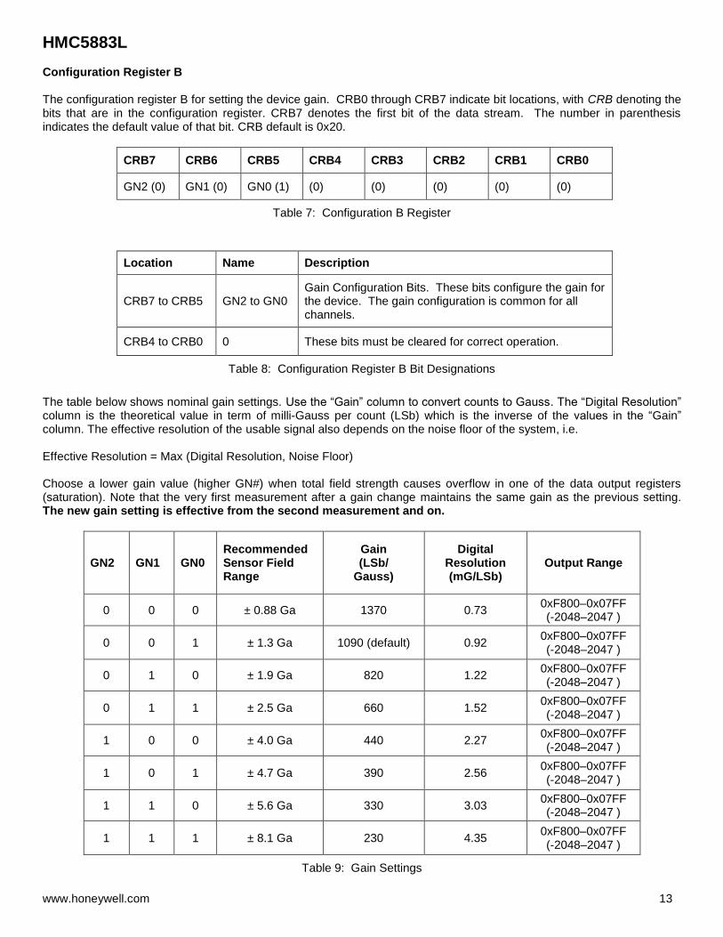
Configuration Register B The configuration register B for setting the device gain. CRB0 through CRB7 indicate bit locations, with CRB denoting the bits that are in the configuration register. CRB7 denotes the first bit of the data stream. The number in parenthesis indicates the default value of that bit. CRB default is 0x20.
CRB7 CRB6 CRB5 CRB4 CRB3 CRB2 CRB1 CRB0
GN2 (0) GN1 (0) GN0 (1) (0) (0) (0) (0) (0)
Table 7: Configuration B Register
Location Name Description
CRB7 to CRB5 GN2 to GN0 Gain Configuration Bits. These bits configure the gain for the device. The gain configuration is common for all channels.
CRB4 to CRB0 0 These bits must be cleared for correct operation.
Table 8: Configuration Register B Bit Designations
The table below shows nominal gain settings. Use the “Gain” column to convert counts to Gauss. The “Digital Resolution” column is the theoretical value in term of milli-Gauss per count (LSb) which is the inverse of the values in the “Gain” column. The effective resolution of the usable signal also depends on the noise floor of the system, i.e. Effective Resolution = Max (Digital Resolution, Noise Floor) Choose a lower gain value (higher GN#) when total field strength causes overflow in one of the data output registers (saturation). Note that the very first measurement after a gain change maintains the same gain as the previous setting. The new gain setting is effective from the second measurement and on.
GN2 GN1 GN0 Recommended Sensor Field Range
Gain (LSb/
Gauss)
Digital Resolution (mG/LSb)
Output Range
0 0 0 ± 0.88 Ga 1370 0.73 0xF800–0x07FF (-2048–2047 )
0 0 1 ± 1.3 Ga 1090 (default) 0.92 0xF800–0x07FF (-2048–2047 )
0 1 0 ± 1.9 Ga 820 1.22 0xF800–0x07FF (-2048–2047 )
0 1 1 ± 2.5 Ga 660 1.52 0xF800–0x07FF (-2048–2047 )
1 0 0 ± 4.0 Ga 440 2.27 0xF800–0x07FF (-2048–2047 )
1 0 1 ± 4.7 Ga 390 2.56 0xF800–0x07FF (-2048–2047 )
1 1 0 ± 5.6 Ga 330 3.03 0xF800–0x07FF (-2048–2047 )
1 1 1 ± 8.1 Ga 230 4.35 0xF800–0x07FF (-2048–2047 )
Table 9: Gain Settings
HMC5883L
14 www.honeywell.com
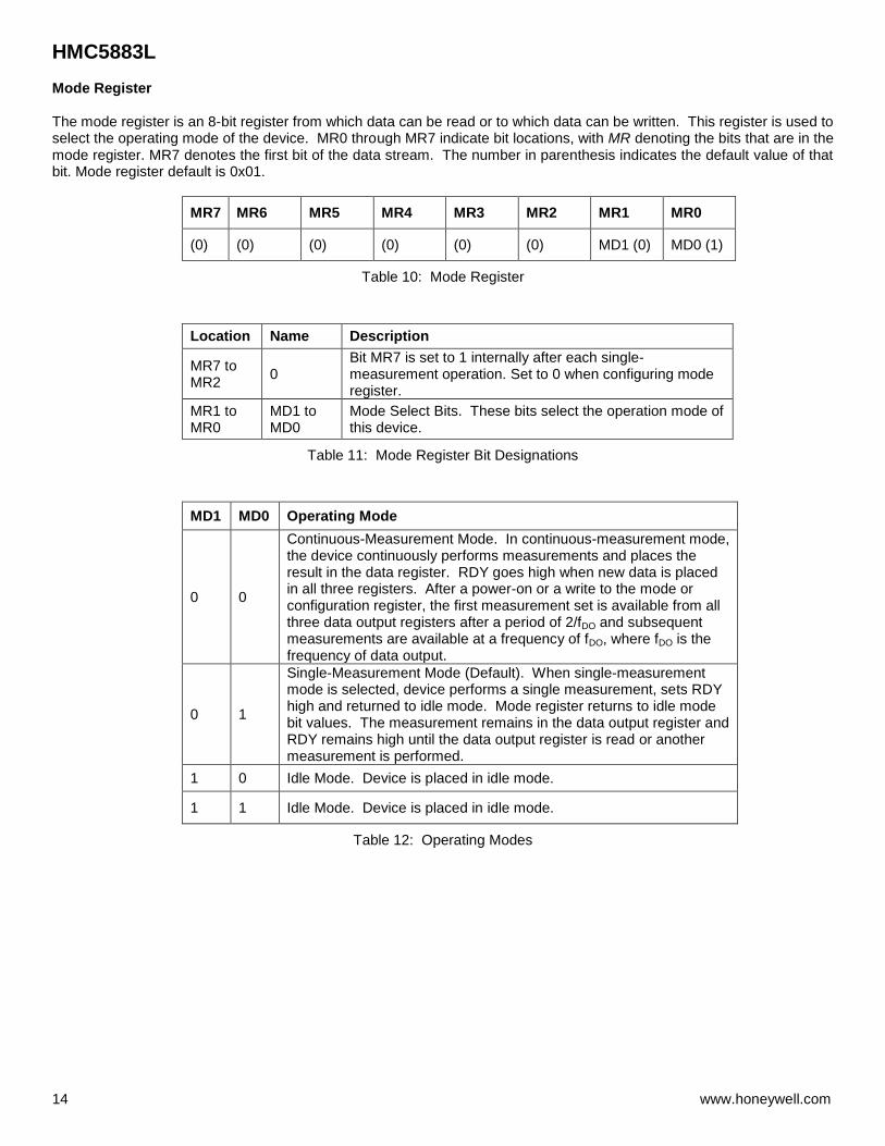
Mode Register The mode register is an 8-bit register from which data can be read or to which data can be written. This register is used to select the operating mode of the device. MR0 through MR7 indicate bit locations, with MR denoting the bits that are in the mode register. MR7 denotes the first bit of the data stream. The number in parenthesis indicates the default value of that bit. Mode register default is 0x01.
MR7 MR6 MR5 MR4 MR3 MR2 MR1 MR0
(0) (0) (0) (0) (0) (0) MD1 (0) MD0 (1)
Table 10: Mode Register
Location Name Description
MR7 to MR2
0 Bit MR7 is set to 1 internally after each single-measurement operation. Set to 0 when configuring mode register.
MR1 to MR0
MD1 to MD0
Mode Select Bits. These bits select the operation mode of this device.
Table 11: Mode Register Bit Designations
MD1 MD0 Operating Mode
0 0
Continuous-Measurement Mode. In continuous-measurement mode, the device continuously performs measurements and places the result in the data register. RDY goes high when new data is placed in all three registers. After a power-on or a write to the mode or configuration register, the first measurement set is available from all three data output registers after a period of 2/fDO and subsequent measurements are available at a frequency of fDO, where fDO is the frequency of data output.
0 1
Single-Measurement Mode (Default). When single-measurement mode is selected, device performs a single measurement, sets RDY high and returned to idle mode. Mode register returns to idle mode bit values. The measurement remains in the data output register and RDY remains high until the data output register is read or another measurement is performed.
1 0 Idle Mode. Device is placed in idle mode.
1 1 Idle Mode. Device is placed in idle mode.
Table 12: Operating Modes
HMC5883L
www.honeywell.com 15
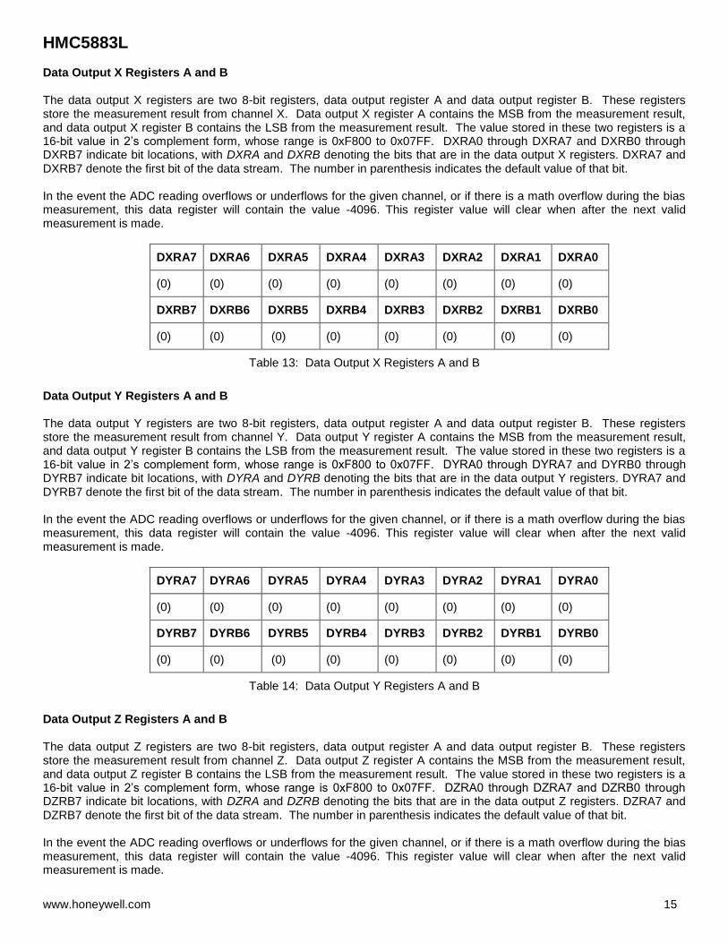
Data Output X Registers A and B The data output X registers are two 8-bit registers, data output register A and data output register B. These registers store the measurement result from channel X. Data output X register A contains the MSB from the measurement result, and data output X register B contains the LSB from the measurement result. The value stored in these two registers is a 16-bit value in 2’s complement form, whose range is 0xF800 to 0x07FF. DXRA0 through DXRA7 and DXRB0 through DXRB7 indicate bit locations, with DXRA and DXRB denoting the bits that are in the data output X registers. DXRA7 and DXRB7 denote the first bit of the data stream. The number in parenthesis indicates the default value of that bit. In the event the ADC reading overflows or underflows for the given channel, or if there is a math overflow during the bias measurement, this data register will contain the value -4096. This register value will clear when after the next valid measurement is made.
DXRA7 DXRA6 DXRA5 DXRA4 DXRA3 DXRA2 DXRA1 DXRA0
(0) (0) (0) (0) (0) (0) (0) (0)
DXRB7 DXRB6 DXRB5 DXRB4 DXRB3 DXRB2 DXRB1 DXRB0
(0) (0) (0) (0) (0) (0) (0) (0)
Table 13: Data Output X Registers A and B
Data Output Y Registers A and B The data output Y registers are two 8-bit registers, data output register A and data output register B. These registers store the measurement result from channel Y. Data output Y register A contains the MSB from the measurement result, and data output Y register B contains the LSB from the measurement result. The value stored in these two registers is a 16-bit value in 2’s complement form, whose range is 0xF800 to 0x07FF. DYRA0 through DYRA7 and DYRB0 through DYRB7 indicate bit locations, with DYRA and DYRB denoting the bits that are in the data output Y registers. DYRA7 and DYRB7 denote the first bit of the data stream. The number in parenthesis indicates the default value of that bit. In the event the ADC reading overflows or underflows for the given channel, or if there is a math overflow during the bias measurement, this data register will contain the value -4096. This register value will clear when after the next valid measurement is made.
DYRA7 DYRA6 DYRA5 DYRA4 DYRA3 DYRA2 DYRA1 DYRA0
(0) (0) (0) (0) (0) (0) (0) (0)
DYRB7 DYRB6 DYRB5 DYRB4 DYRB3 DYRB2 DYRB1 DYRB0
(0) (0) (0) (0) (0) (0) (0) (0)
Table 14: Data Output Y Registers A and B
Data Output Z Registers A and B The data output Z registers are two 8-bit registers, data output register A and data output register B. These registers store the measurement result from channel Z. Data output Z register A contains the MSB from the measurement result, and data output Z register B contains the LSB from the measurement result. The value stored in these two registers is a 16-bit value in 2’s complement form, whose range is 0xF800 to 0x07FF. DZRA0 through DZRA7 and DZRB0 through DZRB7 indicate bit locations, with DZRA and DZRB denoting the bits that are in the data output Z registers. DZRA7 and DZRB7 denote the first bit of the data stream. The number in parenthesis indicates the default value of that bit. In the event the ADC reading overflows or underflows for the given channel, or if there is a math overflow during the bias measurement, this data register will contain the value -4096. This register value will clear when after the next valid measurement is made.
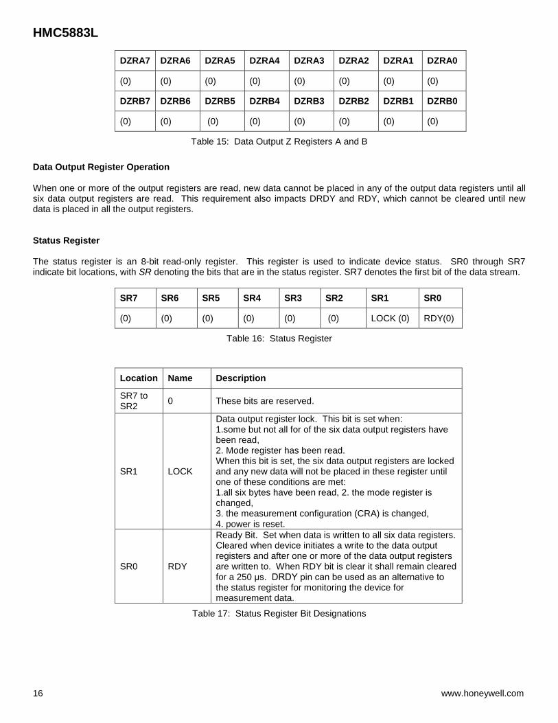
HMC5883L
16 www.honeywell.com
DZRA7 DZRA6 DZRA5 DZRA4 DZRA3 DZRA2 DZRA1 DZRA0
(0) (0) (0) (0) (0) (0) (0) (0)
DZRB7 DZRB6 DZRB5 DZRB4 DZRB3 DZRB2 DZRB1 DZRB0
(0) (0) (0) (0) (0) (0) (0) (0)
Table 15: Data Output Z Registers A and B
Data Output Register Operation When one or more of the output registers are read, new data cannot be placed in any of the output data registers until all six data output registers are read. This requirement also impacts DRDY and RDY, which cannot be cleared until new data is placed in all the output registers.
Status Register The status register is an 8-bit read-only register. This register is used to indicate device status. SR0 through SR7 indicate bit locations, with SR denoting the bits that are in the status register. SR7 denotes the first bit of the data stream.
SR7 SR6 SR5 SR4 SR3 SR2 SR1 SR0
(0) (0) (0) (0) (0) (0) LOCK (0) RDY(0)
Table 16: Status Register
Location Name Description
SR7 to SR2
0 These bits are reserved.
SR1 LOCK
Data output register lock. This bit is set when: 1.some but not all for of the six data output registers have been read, 2. Mode register has been read. When this bit is set, the six data output registers are locked and any new data will not be placed in these register until one of these conditions are met: 1.all six bytes have been read, 2. the mode register is changed, 3. the measurement configuration (CRA) is changed, 4. power is reset.
SR0 RDY
Ready Bit. Set when data is written to all six data registers. Cleared when device initiates a write to the data output registers and after one or more of the data output registers are written to. When RDY bit is clear it shall remain cleared for a 250 μs. DRDY pin can be used as an alternative to the status register for monitoring the device for measurement data.
Table 17: Status Register Bit Designations
HMC5883L
www.honeywell.com 17
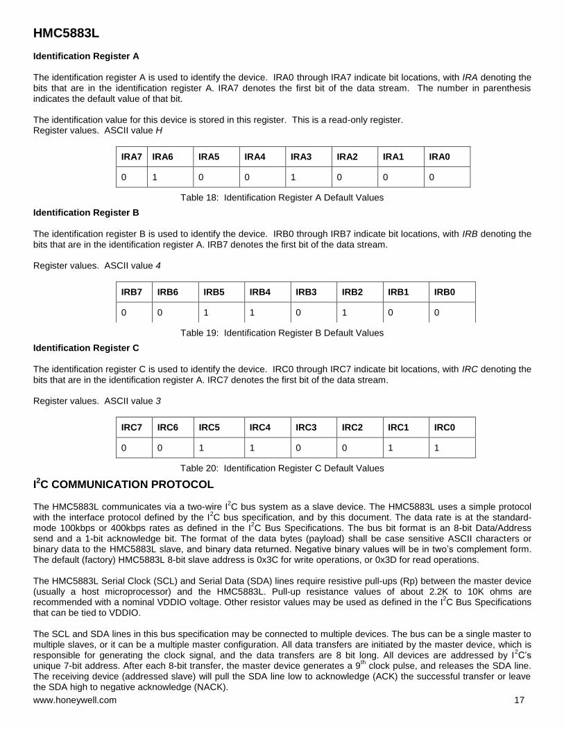
Identification Register A The identification register A is used to identify the device. IRA0 through IRA7 indicate bit locations, with IRA denoting the bits that are in the identification register A. IRA7 denotes the first bit of the data stream. The number in parenthesis indicates the default value of that bit. The identification value for this device is stored in this register. This is a read-only register. Register values. ASCII value H
IRA7 IRA6 IRA5 IRA4 IRA3 IRA2 IRA1 IRA0
0 1 0 0 1 0 0 0
Table 18: Identification Register A Default Values
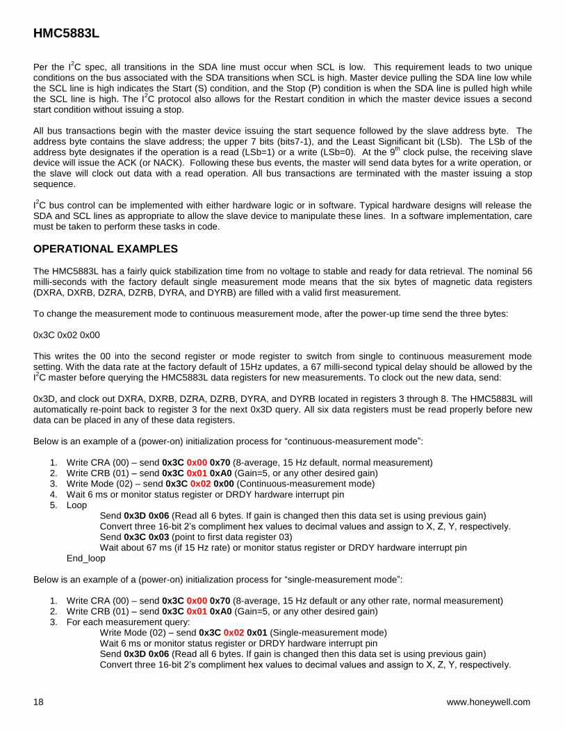
Identification Register B The identification register B is used to identify the device. IRB0 through IRB7 indicate bit locations, with IRB denoting the bits that are in the identification register A. IRB7 denotes the first bit of the data stream. Register values. ASCII value 4
Table 19: Identification Register B Default Values
Identification Register C The identification register C is used to identify the device. IRC0 through IRC7 indicate bit locations, with IRC denoting the bits that are in the identification register A. IRC7 denotes the first bit of the data stream. Register values. ASCII value 3
Table 20: Identification Register C Default Values
I2C COMMUNICATION PROTOCOL
The HMC5883L communicates via a two-wire I2C bus system as a slave device. The HMC5883L uses a simple protocol
with the interface protocol defined by the I2C bus specification, and by this document. The data rate is at the standard-
mode 100kbps or 400kbps rates as defined in the I2C Bus Specifications. The bus bit format is an 8-bit Data/Address
send and a 1-bit acknowledge bit. The format of the data bytes (payload) shall be case sensitive ASCII characters or binary data to the HMC5883L slave, and binary data returned. Negative binary values will be in two’s complement form. The default (factory) HMC5883L 8-bit slave address is 0x3C for write operations, or 0x3D for read operations. The HMC5883L Serial Clock (SCL) and Serial Data (SDA) lines require resistive pull-ups (Rp) between the master device (usually a host microprocessor) and the HMC5883L. Pull-up resistance values of about 2.2K to 10K ohms are recommended with a nominal VDDIO voltage. Other resistor values may be used as defined in the I
2C Bus Specifications
that can be tied to VDDIO. The SCL and SDA lines in this bus specification may be connected to multiple devices. The bus can be a single master to multiple slaves, or it can be a multiple master configuration. All data transfers are initiated by the master device, which is responsible for generating the clock signal, and the data transfers are 8 bit long. All devices are addressed by I
2C’s
unique 7-bit address. After each 8-bit transfer, the master device generates a 9th clock pulse, and releases the SDA line.
The receiving device (addressed slave) will pull the SDA line low to acknowledge (ACK) the successful transfer or leave the SDA high to negative acknowledge (NACK).
IRB7 IRB6 IRB5 IRB4 IRB3 IRB2 IRB1 IRB0
0 0 1 1 0 1 0 0
IRC7 IRC6 IRC5 IRC4 IRC3 IRC2 IRC1 IRC0
0 0 1 1 0 0 1 1
HMC5883L
18 www.honeywell.com
Per the I
2C spec, all transitions in the SDA line must occur when SCL is low. This requirement leads to two unique
conditions on the bus associated with the SDA transitions when SCL is high. Master device pulling the SDA line low while the SCL line is high indicates the Start (S) condition, and the Stop (P) condition is when the SDA line is pulled high while the SCL line is high. The I
2C protocol also allows for the Restart condition in which the master device issues a second
start condition without issuing a stop. All bus transactions begin with the master device issuing the start sequence followed by the slave address byte. The address byte contains the slave address; the upper 7 bits (bits7-1), and the Least Significant bit (LSb). The LSb of the address byte designates if the operation is a read (LSb=1) or a write (LSb=0). At the 9
th clock pulse, the receiving slave
device will issue the ACK (or NACK). Following these bus events, the master will send data bytes for a write operation, or the slave will clock out data with a read operation. All bus transactions are terminated with the master issuing a stop sequence. I2C bus control can be implemented with either hardware logic or in software. Typical hardware designs will release the
SDA and SCL lines as appropriate to allow the slave device to manipulate these lines. In a software implementation, care must be taken to perform these tasks in code.
OPERATIONAL EXAMPLES The HMC5883L has a fairly quick stabilization time from no voltage to stable and ready for data retrieval. The nominal 56 milli-seconds with the factory default single measurement mode means that the six bytes of magnetic data registers (DXRA, DXRB, DZRA, DZRB, DYRA, and DYRB) are filled with a valid first measurement. To change the measurement mode to continuous measurement mode, after the power-up time send the three bytes: 0x3C 0x02 0x00 This writes the 00 into the second register or mode register to switch from single to continuous measurement mode setting. With the data rate at the factory default of 15Hz updates, a 67 milli-second typical delay should be allowed by the I2C master before querying the HMC5883L data registers for new measurements. To clock out the new data, send:
0x3D, and clock out DXRA, DXRB, DZRA, DZRB, DYRA, and DYRB located in registers 3 through 8. The HMC5883L will automatically re-point back to register 3 for the next 0x3D query. All six data registers must be read properly before new data can be placed in any of these data registers. Below is an example of a (power-on) initialization process for “continuous-measurement mode”:
1. Write CRA (00) – send 0x3C 0x00 0x70 (8-average, 15 Hz default, normal measurement) 2. Write CRB (01) – send 0x3C 0x01 0xA0 (Gain=5, or any other desired gain) 3. Write Mode (02) – send 0x3C 0x02 0x00 (Continuous-measurement mode) 4. Wait 6 ms or monitor status register or DRDY hardware interrupt pin 5. Loop
Send 0x3D 0x06 (Read all 6 bytes. If gain is changed then this data set is using previous gain) Convert three 16-bit 2’s compliment hex values to decimal values and assign to X, Z, Y, respectively. Send 0x3C 0x03 (point to first data register 03) Wait about 67 ms (if 15 Hz rate) or monitor status register or DRDY hardware interrupt pin
End_loop Below is an example of a (power-on) initialization process for “single-measurement mode”:
1. Write CRA (00) – send 0x3C 0x00 0x70 (8-average, 15 Hz default or any other rate, normal measurement) 2. Write CRB (01) – send 0x3C 0x01 0xA0 (Gain=5, or any other desired gain) 3. For each measurement query:
Write Mode (02) – send 0x3C 0x02 0x01 (Single-measurement mode) Wait 6 ms or monitor status register or DRDY hardware interrupt pin Send 0x3D 0x06 (Read all 6 bytes. If gain is changed then this data set is using previous gain) Convert three 16-bit 2’s compliment hex values to decimal values and assign to X, Z, Y, respectively.
HMC5883L
www.honeywell.com 19
SELF TEST OPERATION To check the HMC5883L for proper operation, a self test feature in incorporated in which the sensor offset straps are excited to create a nominal field strength (bias field) to be measured. To implement self test, the least significant bits (MS1 and MS0) of configuration register A are changed from 00 to 01 (positive bias) or 10 (negetive bias). Then, by placing the mode register into single or continuous-measurement mode, two data acquisition cycles will be made on each magnetic vector. The first acquisition will be a set pulse followed shortly by measurement data of the external field. The second acquisition will have the offset strap excited (about 10 mA) in the positive bias mode for X, Y, and Z axes to create about a 1.1 gauss self test field plus the external field. The first acquisition values will be subtracted from the second acquisition, and the net measurement will be placed into the data output registers. Since self test adds ~1.1 Gauss additional field to the existing field strength, using a reduced gain setting prevents sensor from being saturated and data registers overflowed. For example, if the configuration register B is set to 0xA0 (Gain=5), values around +452 LSb (1.16 Ga * 390 LSb/Ga) will be placed in the X and Y data output registers and around +421 (1.08 Ga * 390 LSb/Ga) will be placed in Z data output register. To leave the self test mode, change MS1 and MS0 bit of the configuration register A back to 00 (Normal Measurement Mode). Acceptable limits of the self test values depend on the gain setting. Limits for Gain=5 is provided in the specification table. Below is an example of a “positive self test” process using continuous-measurement mode:
1. Write CRA (00) – send 0x3C 0x00 0x71 (8-average, 15 Hz default, positive self test measurement) 2. Write CRB (01) – send 0x3C 0x01 0xA0 (Gain=5) 3. Write Mode (02) – send 0x3C 0x02 0x00 (Continuous-measurement mode) 4. Wait 6 ms or monitor status register or DRDY hardware interrupt pin 5. Loop
Send 0x3D 0x06 (Read all 6 bytes. If gain is changed then this data set is using previous gain) Convert three 16-bit 2’s compliment hex values to decimal values and assign to X, Z, Y, respectively. Send 0x3C 0x03 (point to first data register 03) Wait about 67 ms (if 15 Hz rate) or monitor status register or DRDY hardware interrupt pin
End_loop 6. Check limits –
If all 3 axes (X, Y, and Z) are within reasonable limits (243 to 575 for Gain=5, adjust these limits basing on the gain setting used. See an example below.) Then All 3 axes pass positive self test Write CRA (00) – send 0x3C 0x00 0x70 (Exit self test mode and this procedure) Else
If Gain<7 Write CRB (01) – send 0x3C 0x01 0x_0 (Increase gain setting and retry, skip the next data set)
Else At least one axis did not pass positive self test Write CRA (00) – send 0x3C 0x00 0x70 (Exit self test mode and this procedure)
End If Below is an example of how to adjust the “positive self” test limits basing on the gain setting:
1. If Gain = 6, self test limits are: Low Limit = 243 * 330/390 = 206 High Limit = 575 * 330/390 = 487
2. If Gain = 7, self test limits are: Low Limit = 243 * 230/390 = 143 High Limit = 575 * 230/390 = 339
HMC5883L
20 www.honeywell.com
SCALE FACTOR TEMPERATURE COMPENSATION The built-in self test can also be used to periodically compensate the scaling errors due to temperature variations. A compensation factor can be found by comparing the self test outputs with the ones obtained at a known temperature. For example, if the self test output is 400 at room temperature and 300 at the current temperature then a compensation factor of (400/300) should be applied to all current magnetic readings. A temperature sensor is not required using this method.
Below is an example of a temperature compensation process using positive self test method:
1. If self test measurement at a temperature “when the last magnetic calibration was done”: X_STP = 400 Y_STP = 410 Z_STP = 420
2. If self test measurement at a different tmperature: X_STP = 300 (Lower than before) Y_STP = 310 (Lower than before) Z_STP = 320 (Lower than before)
Then X_TempComp = 400/300 Y_TempComp = 410/310 Z_TempComp = 420/320
3. Applying to all new measurements: X = X * X_TempComp Y = Y * Y_TempComp Z = Z * Z_TempComp
Now all 3 axes are temperature compensated, i.e. sensitivity is same as “when the last magnetic calibration was done”; therefore, the calibration coefficients can be applied without modification.
4. Repeat this process periodically or,for every Δt degrees of temperature change measured, if available.
ORDERING INFORMATION
Ordering Number Product HMC5883L-TR
Tape and Reel 4k pieces/reel
FIND OUT MORE For more information on Honeywell’s Magnetic Sensors visit us online at www.honeywell.com/magneticsensors or contact us at 800-323-8295 (763-954-2474 internationally). The application circuits herein constitute typical usage and interface of Honeywell product. Honeywell does not warranty or assume liability of customer-designed circuits derived from this description or depiction. Honeywell reserves the right to make changes to improve reliability, function or design. Honeywell does not assume any liability arising out of the application or use of any product or circuit described herein; neither does it convey any license under its patent rights nor the rights of others. U.S. Patents 4,441,072, 4,533,872, 4,569,742, 4,681,812, 4,847,584 and 6,529,114 apply to the technology described
Honeywell 12001 Highway 55 Plymouth, MN 55441 Tel: 800-323-8295 www.honeywell.com/magneticsensors
Form # 900405 Rev D March 2011 ©2010 Honeywell International Inc.


![Voigt Airy surface magneto plasmons - ntu.edu.sg Hu_OE_Voigt A… · εε ε εVxx xzxx=+ [15]. ksmp is the propagation constant of the SMPs, calculated by a transcendental equation:](https://static.fdocument.org/doc/165x107/5aba3d3c7f8b9a441d8b677f/voigt-airy-surface-magneto-plasmons-ntuedusg-huoevoigt-a-vxx-xzxx.jpg)