2ch High Side Switch ICs Current Limit High Side Switch...
34
SOP-J8 4.90mm x 6.00mm x 1.65mm SOP8 5.00mm x 6.20mm x 1.71mm 2ch High Side Switch ICs Current Limit High Side Switch ICs BD6516F BD6517F BD2042AFJ BD2052AFJ General Description BD6516F, BD6517F, BD2042AFJ and BD2052AFJ are dual channel high side switch ICs with an over current protection for Universal Serial Bus (USB) power supply line. The IC’s switch unit has two channels of N-Channel power MOSFET. Over current detection circuit, thermal shutdown circuit, under voltage lockout and soft start circuit are built in. Features ■ Dual N-MOS High Side Switch ■ Control Input Logic Active-Low: BD6517F, BD2042AFJ Active-High: BD6516F, BD2052AFJ ■ Soft Start Circuit ■ Over Current Detection ■ Thermal Shutdown ■ Under Voltage Lockout ■ Open Drain Error Flag Output ■ Reverse-Current Protection when Switch Off ■ Flag Output Delay Applications USB Hub in Consumer Appliances, Note PC, PC Peripheral Equipment, and so on. Key Specifications Input Voltage Range: BD6516F/BD6517F 3.0V to 5.5V BD2042AFJ/BD2052AFJ 2.7V to 5.5V ON-Resistance: BD6516F/BD6517F 110mΩ(Typ) BD2042AFJ/BD2052AFJ 100mΩ(Typ) Continuous Current: 0.5A Current Limit Threshold: BD6516F/BD6517F 1.2A(Min), 2.5A (Max) BD2042AFJ/BD2052AFJ 0.7A(Min), 1.8A (Max) Standby Current: 0.01μA (Typ) Output Rise Time: 1.8ms (Typ) Operating Temperature Range: BD6516F/BD6517F -25°C to +85°C BD2042AFJ/BD2052AFJ -40°C to +85°C Packages W(Typ) D(Typ) H(Max) Typical Application Circuit Lineup Current Limit Threshold Control Input Logic Package Orderable Part Number Min Typ Max 1.2A 1.65A 2.5A High SOP8 Reel of 2500 BD6516F-E2 1.2A 1.65A 2.5A Low BD6517F-E2 0.7A 1.0A 1.8A High SOP-J8 BD2052AFJ-E2 0.7A 1.0A 1.8A Low BD2042AFJ-E2 GND IN /EN1 (EN1) /OC1 OUT1 OUT2 /OC2 5V(Typ) CL Data /EN2 (EN2) CIN Data CL ○Product structure:Silicon monolithic integrated circuit ○This product has not designed protection against radioactive rays 1/31 www.rohm.com © 2013 ROHM Co., Ltd. All rights reserved. TSZ22111・14・001 TSZ02201-0E3E0H300240-1-2 21.Aug.2014 Rev.003 Datasheet
Transcript of 2ch High Side Switch ICs Current Limit High Side Switch...
SOP-J8 4.90mm x 6.00mm x 1.65mm
SOP8 5.00mm x 6.20mm x 1.71mm
2ch High Side Switch ICs
Current Limit High Side Switch ICs BD6516F BD6517F BD2042AFJ BD2052AFJ General Description
BD6516F, BD6517F, BD2042AFJ and BD2052AFJ are dual channel high side switch ICs with an over current protection for Universal Serial Bus (USB) power supply line. The IC’s switch unit has two channels of N-Channel power MOSFET. Over current detection circuit, thermal shutdown circuit, under voltage lockout and soft start circuit are built in.
Features
■ Dual N-MOS High Side Switch ■ Control Input Logic
Active-Low: BD6517F, BD2042AFJ Active-High: BD6516F, BD2052AFJ
■ Soft Start Circuit ■ Over Current Detection ■ Thermal Shutdown ■ Under Voltage Lockout ■ Open Drain Error Flag Output ■ Reverse-Current Protection when Switch Off ■ Flag Output Delay
Applications
USB Hub in Consumer Appliances, Note PC, PC Peripheral Equipment, and so on.
Key Specifications Input Voltage Range:
BD6516F/BD6517F 3.0V to 5.5V BD2042AFJ/BD2052AFJ 2.7V to 5.5V
ON-Resistance: BD6516F/BD6517F 110mΩ(Typ) BD2042AFJ/BD2052AFJ 100mΩ(Typ)
Continuous Current: 0.5A Current Limit Threshold: BD6516F/BD6517F 1.2A(Min), 2.5A (Max)
BD2042AFJ/BD2052AFJ 0.7A(Min), 1.8A (Max) Standby Current: 0.01μA (Typ) Output Rise Time: 1.8ms (Typ) Operating Temperature Range: BD6516F/BD6517F -25°C to +85°C BD2042AFJ/BD2052AFJ -40°C to +85°C
Packages W(Typ) D(Typ) H(Max)
Typical Application Circuit Lineup
Current Limit Threshold Control Input Logic Package Orderable Part Number
Min Typ Max 1.2A 1.65A 2.5A High
SOP8 Reel of 2500
BD6516F-E2 1.2A 1.65A 2.5A Low BD6517F-E2 0.7A 1.0A 1.8A High
SOP-J8 BD2052AFJ-E2
0.7A 1.0A 1.8A Low BD2042AFJ-E2
GND
IN
/EN1 (EN1)
/OC1
OUT1
OUT2
/OC2
5V(Typ)
C L
Data /EN2 (EN2)
C IN
Data
C L
○Product structure:Silicon monolithic integrated circuit ○This product has not designed protection against radioactive rays
1/31 www.rohm.com © 2013 ROHM Co., Ltd. All rights reserved. TSZ22111・14・001
TSZ02201-0E3E0H300240-1-2 21.Aug.2014 Rev.003
Datasheet
BD6516F BD6517F BD2042AFJ BD2052AFJ Datasheet
1
2
8
7
GND
IN
/OC1
OUT1
3 /EN1 (EN1)
4
6
5
OUT2
/OC2 /EN2 (EN2)
Block Diagrams
Pin Configurations
Pin Descriptions
BD6516F/BD6517F BD2042AFJ/BD2052AFJ Pin No. Symbol I / O Pin Function Pin
No. Symbol I / O Pin Function
1, 4 CTRLA CTRLB I
Enable input. Switch on at low level. (BD6517F) Low level input < 0.7V. Switch on at high level. (BD6516F) High level input > 2.5V.
1 GND I Ground.
2, 3 FLAGA FLAGB O
Error flag output. Low at over current, thermal shutdown. Open drain output.
2 IN I Power supply input. Input terminal of the switch and power supply of internal circuit.
5, 8 OUTA OUTB O Switch output.
3, 4
/EN1 /EN2, EN1 EN2
I
Enable input. /EN: Switch on at low level. (BD2042AFJ) Low level input < 0.8V EN: Switch on at high level. (BD2052AFJ) High level input > 2.0V.
6 GND I Ground.
5, 8 /OC2 /OC1 O
Error flag output. Low at over current, thermal shutdown. Open drain output.
7 VDD I Power supply input. Input terminal of the switch and power supply of internal circuit.
6, 7 OUT2
OUT1 O Switch output.
Gate Logic1
OCD1 Charge Pump1
TSD1
UVLO
Charge Pump2
OCD2
Gate Logic2
TSD2
/EN1 EN1
IN
/EN2 EN2
GND
/OC1
OUT1
OUT2
/OC2 Delay
Delay
BD2042AFJ/BD2052AFJ
BD6516F/BD6517F TOP VIEW
BD2042AFJ/BD2052AFJ TOP VIEW
1
2
8
7
CTRLA
FLAGA
OUTA
VDD
3 FLAGB
4 CTRLB
6
5
GND
OUTB
BD6516F/BD6517F
Gate Logic1
OCD1 Charge Pump1
UVLO
Charge Pump2
OCD2
Gate Logic2
TSD
CTRLA
VDD
CTRLB
GND
FLAGA
OUTA
OUTB
FLAGB
Delay
Delay
2/31 www.rohm.com © 2013 ROHM Co., Ltd. All rights reserved. TSZ22111・15・001
TSZ02201-0E3E0H300240-1-2 21.Aug.2014 Rev.003
BD6516F BD6517F BD2042AFJ BD2052AFJ Datasheet
Absolute Maximum Ratings BD6516F/BD6517F
Parameter Symbol Rating Unit
Input Voltage VDD -0.3 to +6.0 V
CTRL Voltage VCTRL -0.3 to VDD+0.3 V
FLAG Voltage VFLAG -0.3 to +6.0 V
Output Voltage VOUT -0.3 to +6.0 V
Storage Temperature Tstg -55 to +150 ºC
Power Dissipation Pd 0.67 (Note 1) W
BD2042AFJ/BD2052AFJ
Parameter Symbol Rating Unit
Input Voltage VIN -0.3 to +6.0 V
EN, /EN Voltage VEN, V/EN -0.3 to +6.0 V
/OC Voltage V/OC -0.3 to +6.0 V
/OC Current IS/OC 10 mA
OUT Voltage VOUT -0.3 to +6.0 V
Storage Temperature Tstg -55 to +150 ºC
Power Dissipation Pd 0.67 (Note 1) W
(Note 1) Mounted on 70mm x 70mm x 1.6mm glass-epoxy PCB. Derating : 5.4mW/ oC above Ta=25 oC Caution: Operating the IC over the absolute maximum ratings may damage the IC. The damage can either be a short circuit between pins or an open circuit between pins and the internal circuitry. Therefore, it is important to consider circuit protection measures, such as adding a fuse, in case the IC is operated over the absolute maximum ratings.
Recommended Operation Conditions
BD6516F/BD6517F
Parameter Symbol Rating
Unit Min Typ Max
Input Voltage VDD 3.0 - 5.5 V Operation Temperature Topr -25 - +85 °C Continuous Output Current ILO 0 - 500 mA
BD2042AFJ/BD2052AFJ
Parameter Symbol Rating
Unit Min Typ Max
Input Voltage VIN 2.7 - 5.5 V Operation Temperature Topr -40 - +85 °C Continuous Output Current ILO 0 - 500 mA
3/31 www.rohm.com © 2013 ROHM Co., Ltd. All rights reserved. TSZ22111・15・001
TSZ02201-0E3E0H300240-1-2 21.Aug.2014 Rev.003
BD6516F BD6517F BD2042AFJ BD2052AFJ Datasheet
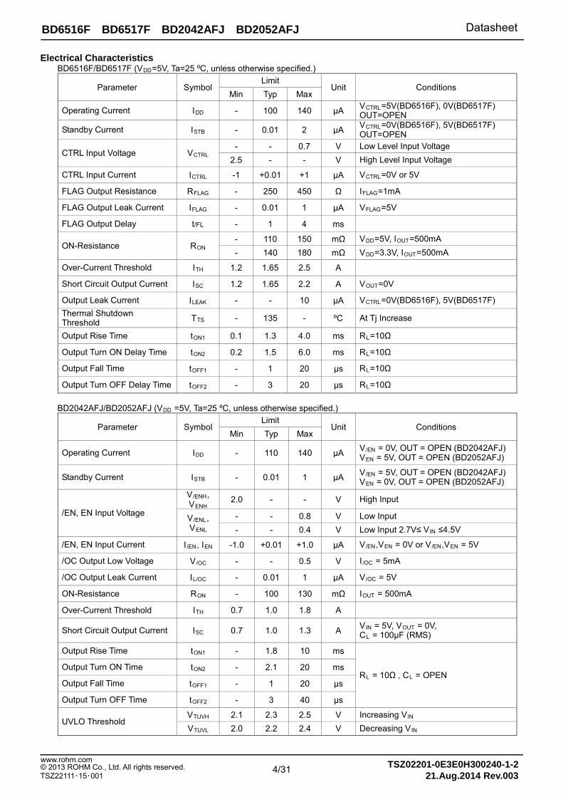
Electrical Characteristics BD6516F/BD6517F (VDD=5V, Ta=25 ºC, unless otherwise specified.)
Parameter Symbol Limit
Unit Conditions Min Typ Max
Operating Current IDD - 100 140 μA VCTRL=5V(BD6516F), 0V(BD6517F) OUT=OPEN
Standby Current ISTB - 0.01 2 μA VCTRL=0V(BD6516F), 5V(BD6517F) OUT=OPEN
CTRL Input Voltage VCTRL - - 0.7 V Low Level Input Voltage
2.5 - - V High Level Input Voltage
CTRL Input Current ICTRL -1 +0.01 +1 μA VCTRL=0V or 5V
FLAG Output Resistance RFLAG - 250 450 Ω IFLAG=1mA
FLAG Output Leak Current IFLAG - 0.01 1 μA VFLAG=5V
FLAG Output Delay t/FL - 1 4 ms
ON-Resistance RON - 110 150 mΩ VDD=5V, IOUT=500mA - 140 180 mΩ VDD=3.3V, IOUT=500mA
Over-Current Threshold ITH 1.2 1.65 2.5 A
Short Circuit Output Current ISC 1.2 1.65 2.2 A VOUT=0V
Output Leak Current ILEAK - - 10 μA VCTRL=0V(BD6516F), 5V(BD6517F) Thermal Shutdown Threshold TTS - 135 - ºC At Tj Increase
Output Rise Time tON1 0.1 1.3 4.0 ms RL=10Ω
Output Turn ON Delay Time tON2 0.2 1.5 6.0 ms RL=10Ω
Output Fall Time tOFF1 - 1 20 μs RL=10Ω
Output Turn OFF Delay Time tOFF2 - 3 20 μs RL=10Ω
BD2042AFJ/BD2052AFJ (VDD =5V, Ta=25 ºC, unless otherwise specified.)
Parameter Symbol Limit
Unit Conditions Min Typ Max
Operating Current IDD - 110 140 μA V/EN = 0V, OUT = OPEN (BD2042AFJ) VEN = 5V, OUT = OPEN (BD2052AFJ)
Standby Current ISTB - 0.01 1 μA V/EN = 5V, OUT = OPEN (BD2042AFJ) VEN = 0V, OUT = OPEN (BD2052AFJ)
/EN, EN Input Voltage
V/ENH, VENH 2.0 - - V High Input
V/ENL, VENL
- - 0.8 V Low Input - - 0.4 V Low Input 2.7V≤ VIN ≤4.5V
/EN, EN Input Current I/EN, IEN -1.0 +0.01 +1.0 μA V/EN,VEN = 0V or V/EN,VEN = 5V
/OC Output Low Voltage V/OC - - 0.5 V I/OC = 5mA
/OC Output Leak Current IL/OC - 0.01 1 μA V/OC = 5V
ON-Resistance RON - 100 130 mΩ IOUT = 500mA
Over-Current Threshold ITH 0.7 1.0 1.8 A
Short Circuit Output Current ISC 0.7 1.0 1.3 A VIN = 5V, VOUT = 0V, CL = 100μF (RMS)
Output Rise Time tON1 - 1.8 10 ms
RL = 10Ω , CL = OPEN Output Turn ON Time tON2 - 2.1 20 ms
Output Fall Time tOFF1 - 1 20 μs
Output Turn OFF Time tOFF2 - 3 40 μs
UVLO Threshold VTUVH 2.1 2.3 2.5 V Increasing VIN VTUVL 2.0 2.2 2.4 V Decreasing VIN
4/31 www.rohm.com © 2013 ROHM Co., Ltd. All rights reserved. TSZ22111・15・001
TSZ02201-0E3E0H300240-1-2 21.Aug.2014 Rev.003
BD6516F BD6517F BD2042AFJ BD2052AFJ Datasheet
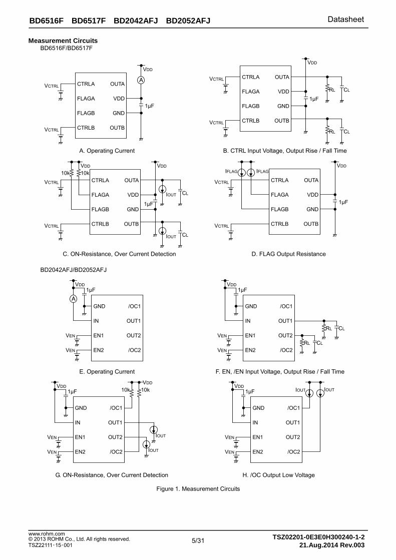
Measurement Circuits BD6516F/BD6517F
CTRLA
FLAGA
FLAGB
CTRLB
OUTA
VDD
GND
OUTB
VDD
1µF
VCTRL
VCTRL
A
CTRLA
FLAGA
FLAGB
CTRLB
OUTA
VDD
GND
OUTB
VDD
1µF
VCTRL
VCTRL
RL CL
RL CL
A. Operating Current B. CTRL Input Voltage, Output Rise / Fall Time
CTRLA
FLAGA
FLAGB
CTRLB
OUTA
VDD
GND
OUTB
VDD
1µF
VCTRL
CL
CL
VDD
VCTRL
10k 10k
IOUT
IOUT
CTRLA
FLAGA
FLAGB
CTRLB
OUTA
VDD
GND
OUTB
VDD
1µF
VCTRL
VCTRL
IFLAG IFLAG
C. ON-Resistance, Over Current Detection D. FLAG Output Resistance
BD2042AFJ/BD2052AFJ
GND
IN
EN1
EN2
/OC1
OUT1
OUT2
/OC2
VDD
VEN
A
1µF
VEN
GND
IN
EN1
EN2
/OC1
OUT1
OUT2
/OC2
VDD
VEN
1µF
VEN RL CL
RL CL
E. Operating Current F. EN, /EN Input Voltage, Output Rise / Fall Time
GND
IN
EN1
EN2
/OC1
OUT1
OUT2
/OC2
VDD
VEN
1µF
VEN IOUT
10k 10k VDD
IOUT
GND
IN
EN1
EN2
/OC1
OUT1
OUT2
/OC2
VDD
VEN
1µF
VEN
IOUT IOUT
G. ON-Resistance, Over Current Detection H. /OC Output Low Voltage
Figure 1. Measurement Circuits
5/31 www.rohm.com © 2013 ROHM Co., Ltd. All rights reserved. TSZ22111・15・001
TSZ02201-0E3E0H300240-1-2 21.Aug.2014 Rev.003
BD6516F BD6517F BD2042AFJ BD2052AFJ Datasheet
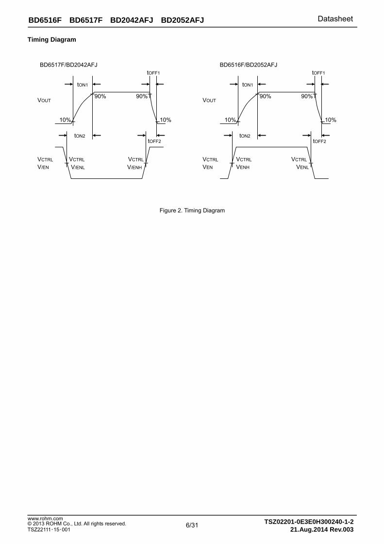
Timing Diagram
BD6517F/BD2042AFJ BD6516F/BD2052AFJ
tON2
VCTRL
tON1
10%
90%
VCTRL
90%
10%
tOFF1
VOUT
VCTRL V/EN
tOFF2
V/ENL V/ENH
tON2
VCTRL
tON1
10%
90%
VCTRL
90%
10%
tOFF1
VOUT
VCTRL VEN
tOFF2
VENH VENL
Figure 2. Timing Diagram
6/31 www.rohm.com © 2013 ROHM Co., Ltd. All rights reserved. TSZ22111・15・001
TSZ02201-0E3E0H300240-1-2 21.Aug.2014 Rev.003
BD6516F BD6517F BD2042AFJ BD2052AFJ Datasheet
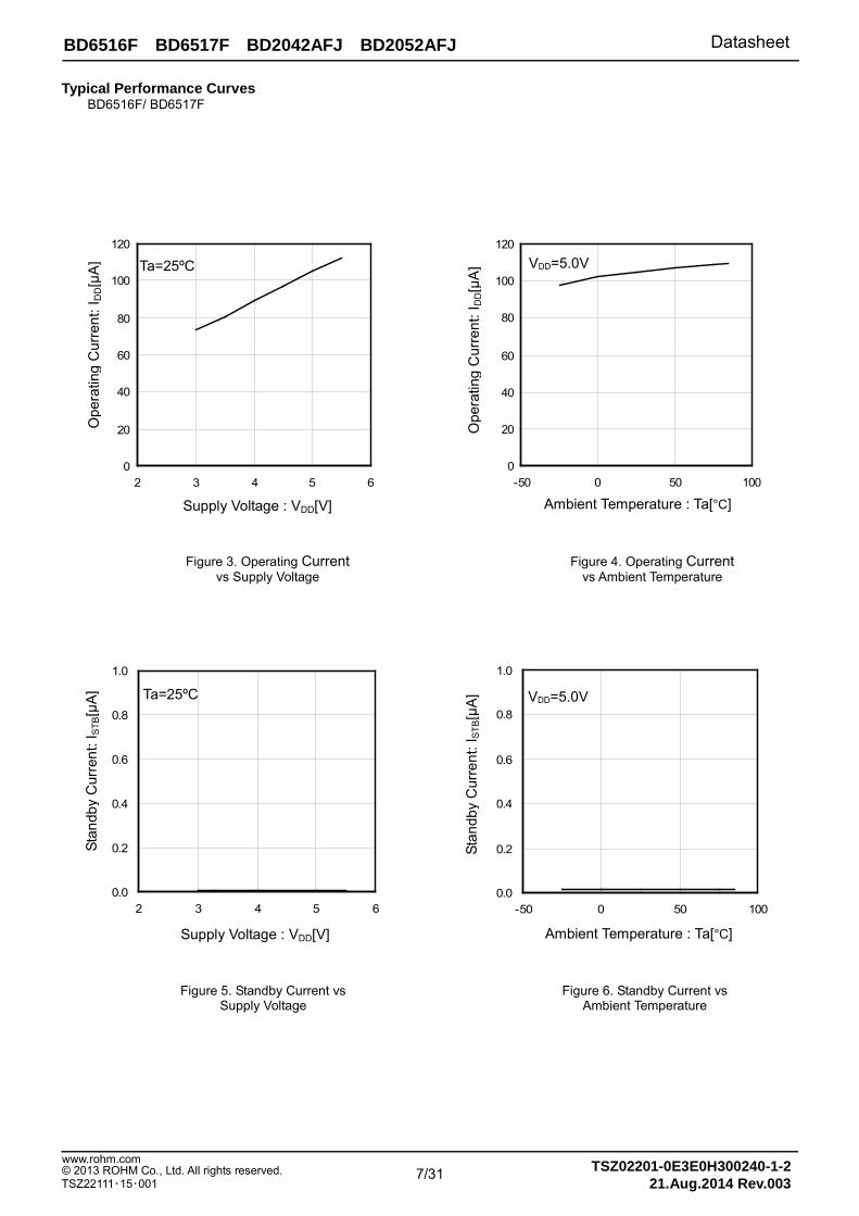
Typical Performance Curves BD6516F/ BD6517F
Figure 3. Operating Current vs Supply Voltage
Figure 4. Operating Current vs Ambient Temperature
0
20
40
60
80
100
120
2 3 4 5 6
SUPPLY VOLTAGE : VDD[V]
OPE
RAT
ING
CU
RR
ENT
: ID
D[u
A]
Ta=25ºC
Ope
ratin
g C
urre
nt: I
DD[μ
A]
Supply Voltage : VDD[V]
0
20
40
60
80
100
120
-50 0 50 100
AMBIENT TEMPERATURE : Ta[℃]
OPE
RAT
ING
CU
RR
ENT
: I D
D[u
A]
VDD=5.0V
Ope
ratin
g C
urre
nt: I
DD[μ
A]
Ambient Temperature : Ta[°C]
0.0
0.2
0.4
0.6
0.8
1.0
2 3 4 5 6
SUPPLY VOLTAGE : VDD[V]
OPE
RAT
ING
CU
RR
ENT
: ID
D[u
A] Ta=25ºC
Stan
dby
Cur
rent
: IS
TB[μ
A]
Supply Voltage : VDD[V]
0.0
0.2
0.4
0.6
0.8
1.0
-50 0 50 100
AMBIENT TEMPERATURE : Ta[℃]
OPE
RAT
ING
CU
RR
ENT
: ID
D[u
A] VDD=5.0V
Stan
dby
Cur
rent
: IS
TB[μ
A]
Ambient Temperature : Ta[°C]
Figure 5. Standby Current vs Supply Voltage
Figure 6. Standby Current vs Ambient Temperature
7/31 www.rohm.com © 2013 ROHM Co., Ltd. All rights reserved. TSZ22111・15・001
TSZ02201-0E3E0H300240-1-2 21.Aug.2014 Rev.003
BD6516F BD6517F BD2042AFJ BD2052AFJ Datasheet
Typical Performance Curves - continued
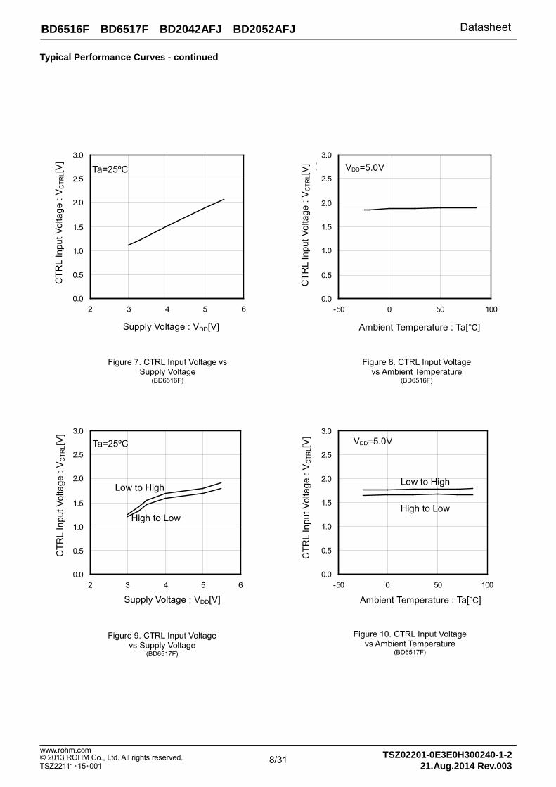
Figure 7. CTRL Input Voltage vs Supply Voltage
(BD6516F)
0.0
0.5
1.0
1.5
2.0
2.5
3.0
2 3 4 5 6
SUPPLY VOLTAGE : VDD[V]
CO
NTR
OL
INPU
T VO
LTAG
E : V
CTR
L [V]
Ta=25ºC
CTR
L In
put V
olta
ge :
V CTR
L[V]
Supply Voltage : VDD[V]
Figure 8. CTRL Input Voltage vs Ambient Temperature
(BD6516F)
0.0
0.5
1.0
1.5
2.0
2.5
3.0
-50 0 50 100
AMBIENT TEMPERATURE : Ta[℃]C
ON
TRO
L IN
PUT
VOLT
AGE
: VC
TRL [V
]
VDD=5.0V
CTR
L In
put V
olta
ge :
V CTR
L[V]
Ambient Temperature : Ta[°C]
0.0
0.5
1.0
1.5
2.0
2.5
3.0
-50 0 50 100
AMBIENT TEMPERATURE : Ta[℃]
CO
NTR
OL
INPU
T VO
LTAG
E : V
CTR
L [V]
Figure 10. CTRL Input Voltage vs Ambient Temperature
(BD6517F)
Figure 9. CTRL Input Voltage vs Supply Voltage
(BD6517F)
0.0
0.5
1.0
1.5
2.0
2.5
3.0
2 3 4 5 6
SUPPLY VOLTAGE : VDD[V]
CO
NTR
OL
INPU
T VO
LTAG
E : V
CTR
L [V]
Ta=25ºC
Low to High
High to Low
CTR
L In
put V
olta
ge :
V CTR
L[V]
CTR
L In
put V
olta
ge :
V CTR
L[V]
Supply Voltage : VDD[V] Ambient Temperature : Ta[°C]
VDD=5.0V
Low to High
High to Low
8/31 www.rohm.com © 2013 ROHM Co., Ltd. All rights reserved. TSZ22111・15・001
TSZ02201-0E3E0H300240-1-2 21.Aug.2014 Rev.003
BD6516F BD6517F BD2042AFJ BD2052AFJ Datasheet
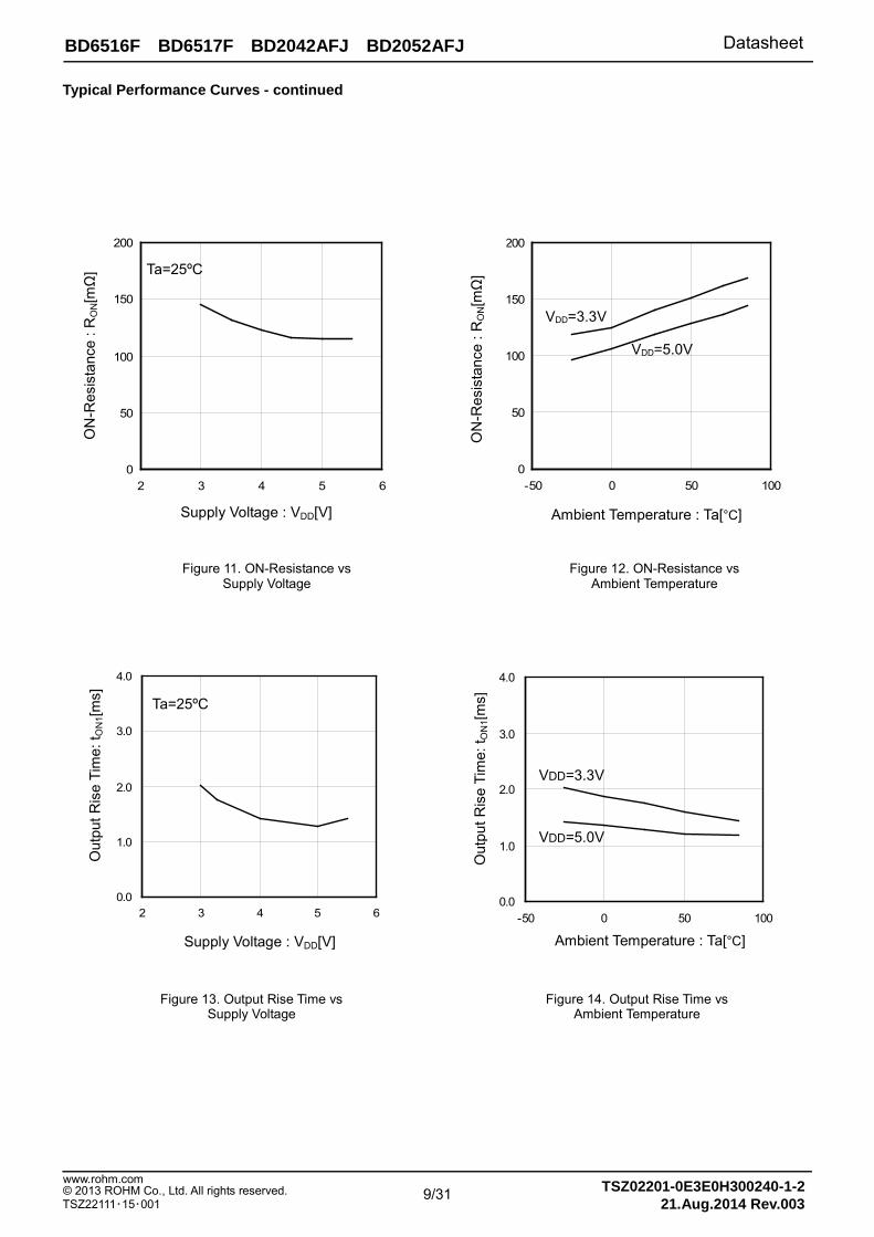
Figure 11. ON-Resistance vs Supply Voltage
0
50
100
150
200
2 3 4 5 6
SUPPLY VOLTAGE : VDD[V]
ON
RES
ISTA
NC
E : R
ON[m
Ω] Ta=25ºC
Typical Performance Curves - continued
Figure 12. ON-Resistance vs Ambient Temperature
0
50
100
150
200
-50 0 50 100
AMBIENT TEMPERATURE : Ta[℃]O
N R
ESIS
TAN
CE
: RO
N[m
Ω]
VDD=3.3V
VDD=5.0V
ON
-Res
ista
nce
: RO
N[m
Ω]
Supply Voltage : VDD[V]
ON
-Res
ista
nce
: RO
N[m
Ω]
Ambient Temperature : Ta[°C]
Figure 13. Output Rise Time vs Supply Voltage
0.0
1.0
2.0
3.0
4.0
2 3 4 5 6
SUPPLY VOLTAGE : VDD[V]
TUR
N O
N R
ISE
TIM
E : T
ON
1[u
s] Ta=25ºC
Figure 14. Output Rise Time vs Ambient Temperature
0.0
1.0
2.0
3.0
4.0
-50 0 50 100
AMBIENT TEMPERATURE : Ta[℃]
TUR
N O
N R
ISE
TIM
E : T
ON
1[u
s]
VDD=3.3V
VDD=5.0V
Out
put R
ise
Tim
e: t O
N1[m
s]
Out
put R
ise
Tim
e: t O
N1[m
s]
Supply Voltage : VDD[V] Ambient Temperature : Ta[°C]
9/31 www.rohm.com © 2013 ROHM Co., Ltd. All rights reserved. TSZ22111・15・001
TSZ02201-0E3E0H300240-1-2 21.Aug.2014 Rev.003
BD6516F BD6517F BD2042AFJ BD2052AFJ Datasheet
Typical Performance Curves - continued
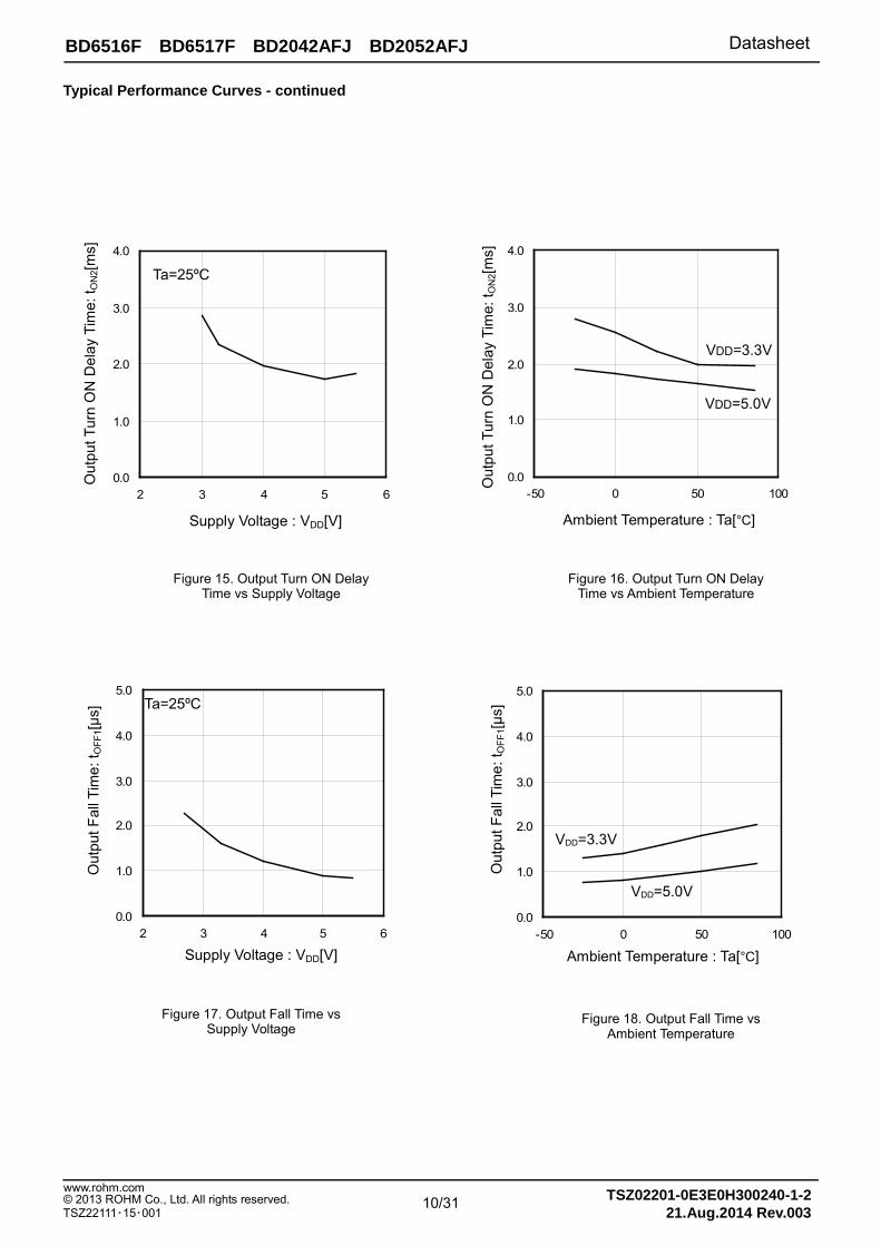
Figure 15. Output Turn ON Delay Time vs Supply Voltage
0.0
1.0
2.0
3.0
4.0
2 3 4 5 6
SUPPLY VOLTAGE : VDD[V]
TUR
N O
N D
ELAY
: T
ON
2[u
s]
Ta=25ºC
Figure 16. Output Turn ON Delay Time vs Ambient Temperature
0.0
1.0
2.0
3.0
4.0
-50 0 50 100
AMBIENT TEMPERATURE : Ta[℃]
TUR
N O
N D
ELAY
: T
ON
2[u
s]
VDD=3.3V
VDD=5.0V
Out
put T
urn
ON
Del
ay T
ime:
t ON
2[ms]
Out
put T
urn
ON
Del
ay T
ime:
t ON
2[ms]
Supply Voltage : VDD[V] Ambient Temperature : Ta[°C]
Figure 17. Output Fall Time vs Supply Voltage
0.0
1.0
2.0
3.0
4.0
5.0
2 3 4 5 6
SUPPLY VOLTAGE : VDD[V]
TUR
N O
FF F
ALL
TIM
E : T
OFF
1 [us]
Ta=25ºC
Figure 18. Output Fall Time vs Ambient Temperature
0.0
1.0
2.0
3.0
4.0
5.0
-50 0 50 100
AMBIENT TEMPERATURE : Ta[℃]
TUR
N O
FF F
ALL
TIM
E : T
OFF
1 [us]
VDD=3.3V
VDD=5.0V
Out
put F
all T
ime:
t OFF
1[μs]
Supply Voltage : VDD[V]
Out
put F
all T
ime:
t OFF
1[μs]
Ambient Temperature : Ta[°C]
10/31 www.rohm.com © 2013 ROHM Co., Ltd. All rights reserved. TSZ22111・15・001
TSZ02201-0E3E0H300240-1-2 21.Aug.2014 Rev.003
BD6516F BD6517F BD2042AFJ BD2052AFJ Datasheet
Typical Performance Curves - continued
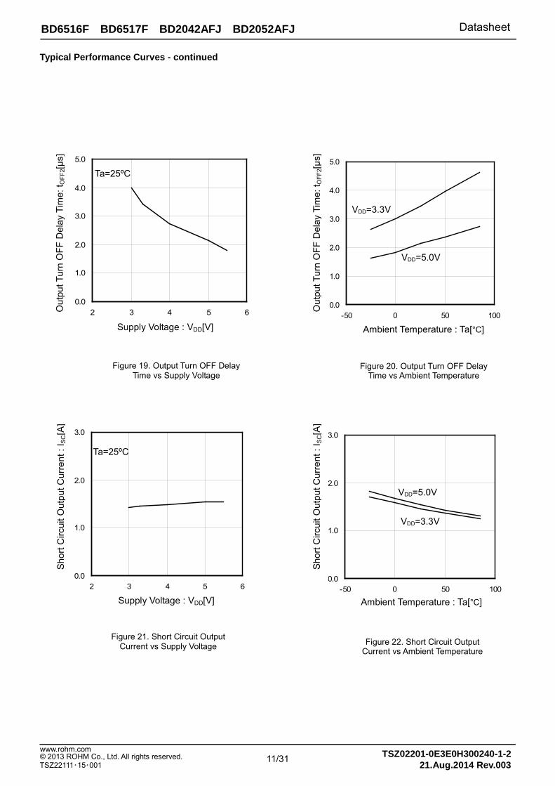
Figure 19. Output Turn OFF Delay Time vs Supply Voltage
0.0
1.0
2.0
3.0
4.0
5.0
2 3 4 5 6
SUPPLY VOLTAGE : VDD[V]
TUR
N O
FF D
ELAY
: TO
FF2 [u
s]
Ta=25ºC
Out
put T
urn
OFF
Del
ay T
ime:
t OFF
2[μs]
Supply Voltage : VDD[V]
Figure 21. Short Circuit Output Current vs Supply Voltage
0.0
1.0
2.0
3.0
2 3 4 5 6
SUPPLY VOLTAGE : VDD[V]
SHO
RT
CIR
CU
IT C
UR
REN
T : I
SC[A
]
Ta=25ºC
Figure 22. Short Circuit Output Current vs Ambient Temperature
0.0
1.0
2.0
3.0
-50 0 50 100
AMBIENT TEMPERATURE : Ta[℃]
SHO
RT
CIR
CU
IT C
UR
REN
T : I
SC[A
]
VDD=5.0V
VDD=3.3V
Figure 20. Output Turn OFF Delay Time vs Ambient Temperature
0.0
1.0
2.0
3.0
4.0
5.0
-50 0 50 100
AMBIENT TEMPERATURE : Ta[℃]TU
RN
OFF
DEL
AY :
TOFF
2 [us]
VDD=3.3V
VDD=5.0V
Out
put T
urn
OFF
Del
ay T
ime:
t OFF
2[μs]
Shor
t Circ
uit O
utpu
t Cur
rent
: I S
C[A
]
Ambient Temperature : Ta[°C]
Supply Voltage : VDD[V]
Shor
t Circ
uit O
utpu
t Cur
rent
: I S
C[A
]
Ambient Temperature : Ta[°C]
11/31 www.rohm.com © 2013 ROHM Co., Ltd. All rights reserved. TSZ22111・15・001
TSZ02201-0E3E0H300240-1-2 21.Aug.2014 Rev.003
BD6516F BD6517F BD2042AFJ BD2052AFJ Datasheet
Typical Performance Curves - continued
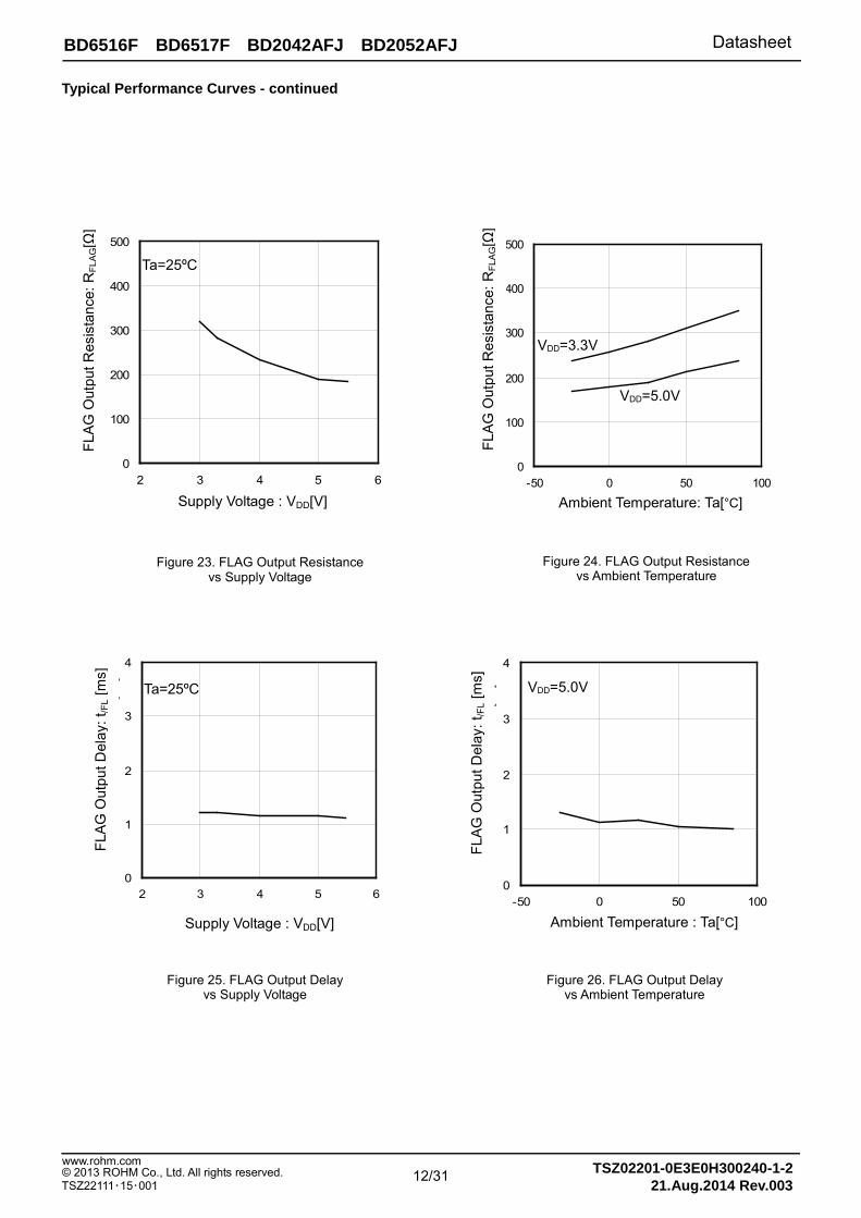
Figure 24. FLAG Output Resistance vs Ambient Temperature
0
100
200
300
400
500
-50 0 50 100
AMBIENT TEMPERATURE : Ta[℃]FL
AG O
UTP
UT
RES
ISTA
NC
E : R
FLAG
[Ω]
VDD=5.0V
VDD=3.3V
FLAG
Out
put R
esis
tanc
e: R
FLA
G[Ω
] Ambient Temperature: Ta[°C]
Figure 23. FLAG Output Resistance vs Supply Voltage
0
100
200
300
400
500
2 3 4 5 6
SUPPLY VOLTAGE : VDD[V]
FLAG
OU
TPU
T R
ESIS
TAN
CE
: RFL
AG[Ω
]
Ta=25ºC
FLAG
Out
put R
esis
tanc
e: R
FLA
G[Ω
]
Supply Voltage : VDD[V]
Figure 25. FLAG Output Delay vs Supply Voltage
0
1
2
3
4
2 3 4 5 6
SUPPLY VOLTAGE : VDD[V]
FLAG
OU
TPU
T D
ELAY
: TD
FL[m
s] Ta=25ºC
FLAG
Out
put D
elay
: t/F
L [m
s]
Supply Voltage : VDD[V]
Figure 26. FLAG Output Delay vs Ambient Temperature
0
1
2
3
4
-50 0 50 100
AMBIENT TEMPERATURE : Ta[℃]
FLAG
OU
TPU
T D
ELAY
: TD
FL[m
s] VDD=5.0V
FLAG
Out
put D
elay
: t/F
L [m
s]
Ambient Temperature : Ta[°C]
12/31 www.rohm.com © 2013 ROHM Co., Ltd. All rights reserved. TSZ22111・15・001
TSZ02201-0E3E0H300240-1-2 21.Aug.2014 Rev.003
BD6516F BD6517F BD2042AFJ BD2052AFJ Datasheet
VIN=5.0V
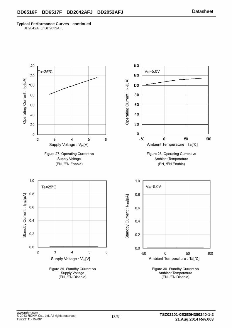
Figure 28. Operating Current vs Ambient Temperature
(EN, /EN Enable)
Figure 27. Operating Current vs Supply Voltage
(EN, /EN Enable)
Ta=25ºC
0.0
0.2
0.4
0.6
0.8
1.0
-50 0 50 100AMBIENT TEMPERATURE : Ta[℃]
OPE
RAT
ING
CU
RR
ENT
: IST
B [uA] VIN=5.0V
Ope
ratin
g C
urre
nt :
I DD[μ
A]
Ope
ratin
g C
urre
nt :
I DD[μ
A]
Supply Voltage : VIN[V] Ambient Temperature : Ta[°C]
Stan
dby
Cur
rent
: I S
TB[μ
A]
Stan
dby
Cur
rent
: I S
TB[μ
A]
Supply Voltage : VIN[V] Ambient Temperature : Ta[°C]
Figure 29. Standby Current vs Supply Voltage
(EN, /EN Disable)
0.0
0.2
0.4
0.6
0.8
1.0
2 3 4 5 6
Ta=25ºC
Typical Performance Curves - continued BD2042AFJ/ BD2052AFJ
Figure 30. Standby Current vs Ambient Temperature
(EN, /EN Disable)
13/31 www.rohm.com © 2013 ROHM Co., Ltd. All rights reserved. TSZ22111・15・001
TSZ02201-0E3E0H300240-1-2 21.Aug.2014 Rev.003
BD6516F BD6517F BD2042AFJ BD2052AFJ Datasheet
0.0
0.5
1.0
1.5
2.0
2 3 4 5 6SUPPLY VOLTAGE : VIN[V]
ENAB
LE IN
PUT
VOLT
AGE
:VE
N, V
/EN[V
] 0 Low to High High to Low
Ta=25ºC
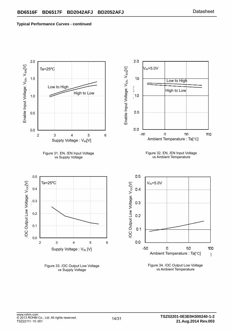
Figure 31. EN, /EN Input Voltage vs Supply Voltage
0.0
0.1
0.2
0.3
0.4
0.5
2 3 4 5 6SUPPLY VOLTAGE : VDD[V]
/OC
OU
TPU
T LO
W V
OLT
AGE
:V/
OC[V
]
Ta=25ºC
Figure 33. /OC Output Low Voltage vs Supply Voltage
VIN=5.0V
Figure 34. /OC Output Low Voltage vs Ambient Temperature
VIN=5.0V
High to Low
Low to High
Figure 32. EN, /EN Input Voltage vs Ambient Temperature
Enab
le In
put V
olta
ge: V
EN, V
/EN[V
]
Enab
le In
put V
olta
ge: V
EN, V
/EN[V
]
Supply Voltage : VIN[V] Ambient Temperature : Ta[°C]
/OC
Out
put L
ow V
olta
ge: V
/OC[V
]
/OC
Out
put L
ow V
olta
ge: V
/OC[V
]
Supply Voltage : VIN [V] Ambient Temperature : Ta[°C]
Typical Performance Curves - continued
14/31 www.rohm.com © 2013 ROHM Co., Ltd. All rights reserved. TSZ22111・15・001
TSZ02201-0E3E0H300240-1-2 21.Aug.2014 Rev.003
BD6516F BD6517F BD2042AFJ BD2052AFJ Datasheet
Typical Performance Curves - continued
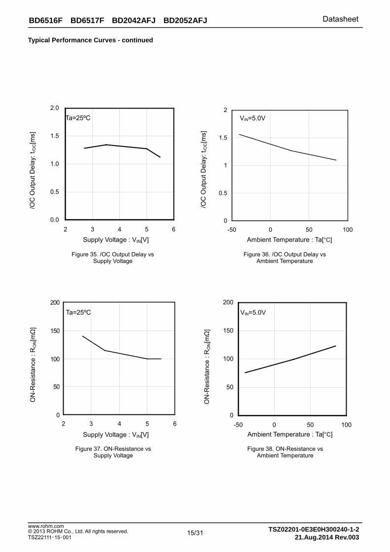
Figure 37. ON-Resistance vs Supply Voltage
0
50
100
150
200
2 3 4 5 6SUPPLY VOLTAGE : VDD[V]
ON
RES
ISTA
NC
E :
RO
N[ m
Ω]
Ta=25ºC
0
50
100
150
200
-50 0 50 100AMBIENT TEMPERATURE : Ta[℃]
VIN=5.0V
Figure 38. ON-Resistance vs Ambient Temperature
ON
-Res
ista
nce
: RO
N[m
Ω]
ON
-Res
ista
nce
: RO
N[m
Ω]
Supply Voltage : VIN[V] Ambient Temperature : Ta[°C]
Figure 35. /OC Output Delay vs Supply Voltage
0.0
0.5
1.0
1.5
2.0
2 3 4 5 6SUPPLY VOLTAGE : VDD[V]
ON
RE
SIS
TAN
CE
:R
ON
[mΩ
]
Ta=25ºC
0
0.5
1
1.5
2
-50 0 50 100
AMBIENT TEMPERATURE : Ta[℃]
ON
RES
ISTA
NC
E :R
ON[m
Ω]
VIN=5.0V
/OC
Out
put D
elay
: t/O
C[m
s]
/OC
Out
put D
elay
: t/O
C[m
s]
Supply Voltage : VIN[V] Ambient Temperature : Ta[°C]
Figure 36. /OC Output Delay vs Ambient Temperature
15/31 www.rohm.com © 2013 ROHM Co., Ltd. All rights reserved. TSZ22111・15・001
TSZ02201-0E3E0H300240-1-2 21.Aug.2014 Rev.003
BD6516F BD6517F BD2042AFJ BD2052AFJ Datasheet
0.0
0.5
1.0
1.5
2.0
-50 0 50 100AMBIENT TEMPERATURE : Ta[℃]
VIN=5.0V
Figure 42. Short Circuit Output Current vs Ambient Temperature
0.0
0.5
1.0
1.5
2.0
2 3 4 5 6SUPPLY VOLTAGE : VIN[V]
SHO
RT
CIR
CU
IT C
UR
REN
T :I
SC[A
]
Ta=25ºC
Figure 41. Short Circuit Output Current vs Supply Voltage
0.0
0.5
1.0
1.5
2.0
2 3 4 5 6SUPPLY VOLTAGE : VIN[V]
SHO
RT
CIR
CU
IT C
UR
REN
T :I
SC[A
]
Ta=25ºC
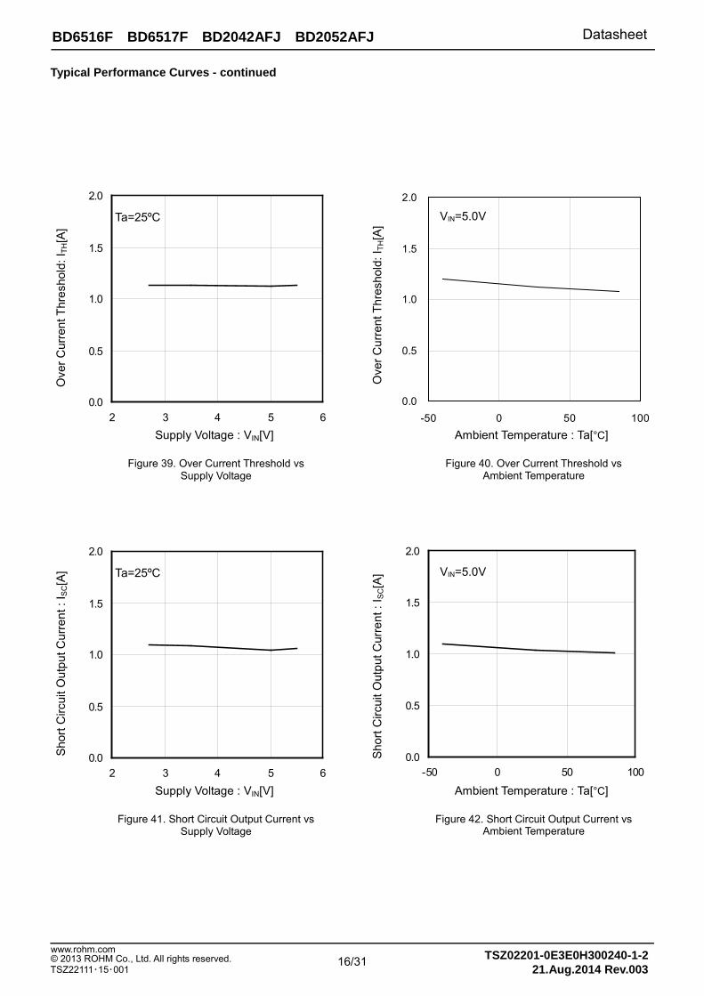
Figure 39. Over Current Threshold vs Supply Voltage
0.0
0.5
1.0
1.5
2.0
-50 0 50 100AMBIENT TEMPERATURE : Ta[℃]
SHO
RT
CIR
CU
IT C
UR
REN
T :
VIN=5.0V
Figure 40. Over Current Threshold vs Ambient Temperature
Typical Performance Curves - continued Sh
ort C
ircui
t Out
put C
urre
nt :
I SC[A
]
Shor
t Circ
uit O
utpu
t Cur
rent
: I S
C[A
]
Supply Voltage : VIN[V] Ambient Temperature : Ta[°C]
Ove
r Cur
rent
Thr
esho
ld: I
TH[A
]
Ove
r Cur
rent
Thr
esho
ld: I
TH[A
]
Supply Voltage : VIN[V] Ambient Temperature : Ta[°C]
16/31 www.rohm.com © 2013 ROHM Co., Ltd. All rights reserved. TSZ22111・15・001
TSZ02201-0E3E0H300240-1-2 21.Aug.2014 Rev.003
BD6516F BD6517F BD2042AFJ BD2052AFJ Datasheet
Typical Performance Curves - continued
0.0
1.0
2.0
3.0
4.0
5.0
-50 0 50 100AMBIENT TEMPERATURE : Ta[℃]
RIS
E TI
ME
:TO
N1 [m
s]
VIN=5.0V
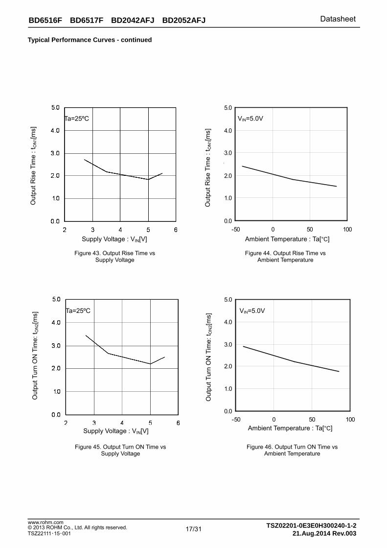
Figure 44. Output Rise Time vs Ambient Temperature
Figure 43. Output Rise Time vs Supply Voltage
Ta=25ºC
Figure 45. Output Turn ON Time vs Supply Voltage
Ta=25ºC
Figure 46. Output Turn ON Time vs Ambient Temperature
0.0
1.0
2.0
3.0
4.0
5.0
-50 0 50 100AMBIENT TEMPERATURE : Ta[℃]
TUR
N O
N T
IME
:TO
N2[m
s]
VIN=5.0V
Out
put R
ise
Tim
e : t
ON
1[ms]
Out
put R
ise
Tim
e : t
ON
1[ms]
Supply Voltage : VIN[V] Ambient Temperature : Ta[°C]
Out
put T
urn
ON
Tim
e: t O
N2[m
s]
Out
put T
urn
ON
Tim
e: t O
N2[m
s]
Supply Voltage : VIN[V] Ambient Temperature : Ta[°C]
17/31 www.rohm.com © 2013 ROHM Co., Ltd. All rights reserved. TSZ22111・15・001
TSZ02201-0E3E0H300240-1-2 21.Aug.2014 Rev.003
BD6516F BD6517F BD2042AFJ BD2052AFJ Datasheet
Typical Performance Curves - continued
0.0
1.0
2.0
3.0
4.0
5.0
2 3 4 5 6SUPPLY VOLTAGE : VIN[V]
FALL
TIM
E :
TOFF
1 [us]
Ta=25ºC
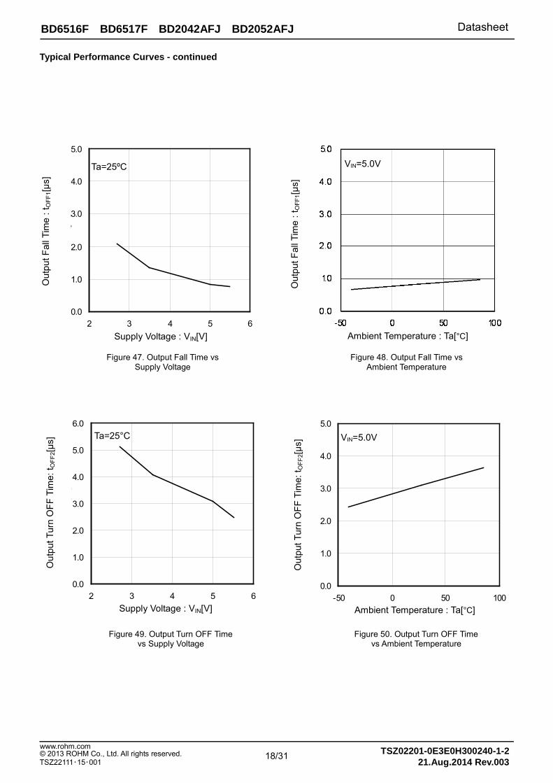
Figure 47. Output Fall Time vs Supply Voltage
VIN=5.0V
Figure 48. Output Fall Time vs Ambient Temperature
Figure 49. Output Turn OFF Time vs Supply Voltage
0.0
1.0
2.0
3.0
4.0
5.0
6.0
2 3 4 5 6SUPPLY VOLTAGE : VIN[V]
TUR
N O
FF T
IME
:TO
FF2 [u
s]
Ta=25°C
0.0
1.0
2.0
3.0
4.0
5.0
-50 0 50 100AMBIENT TEMPERATURE : Ta[℃]
TUR
N O
FF T
IME
:TO
FF2 [u
s]
VIN=5.0V
Figure 50. Output Turn OFF Time vs Ambient Temperature
Out
put F
all T
ime
: tO
FF1[µ
s]
Out
put F
all T
ime
: tO
FF1[µ
s]
Supply Voltage : VIN[V] Ambient Temperature : Ta[°C]
Out
put T
urn
OFF
Tim
e: t O
FF2[µ
s]
Out
put T
urn
OFF
Tim
e: t O
FF2[µ
s]
Supply Voltage : VIN[V] Ambient Temperature : Ta[°C]
18/31 www.rohm.com © 2013 ROHM Co., Ltd. All rights reserved. TSZ22111・15・001
TSZ02201-0E3E0H300240-1-2 21.Aug.2014 Rev.003
BD6516F BD6517F BD2042AFJ BD2052AFJ Datasheet
Typical Performance Curves - continued
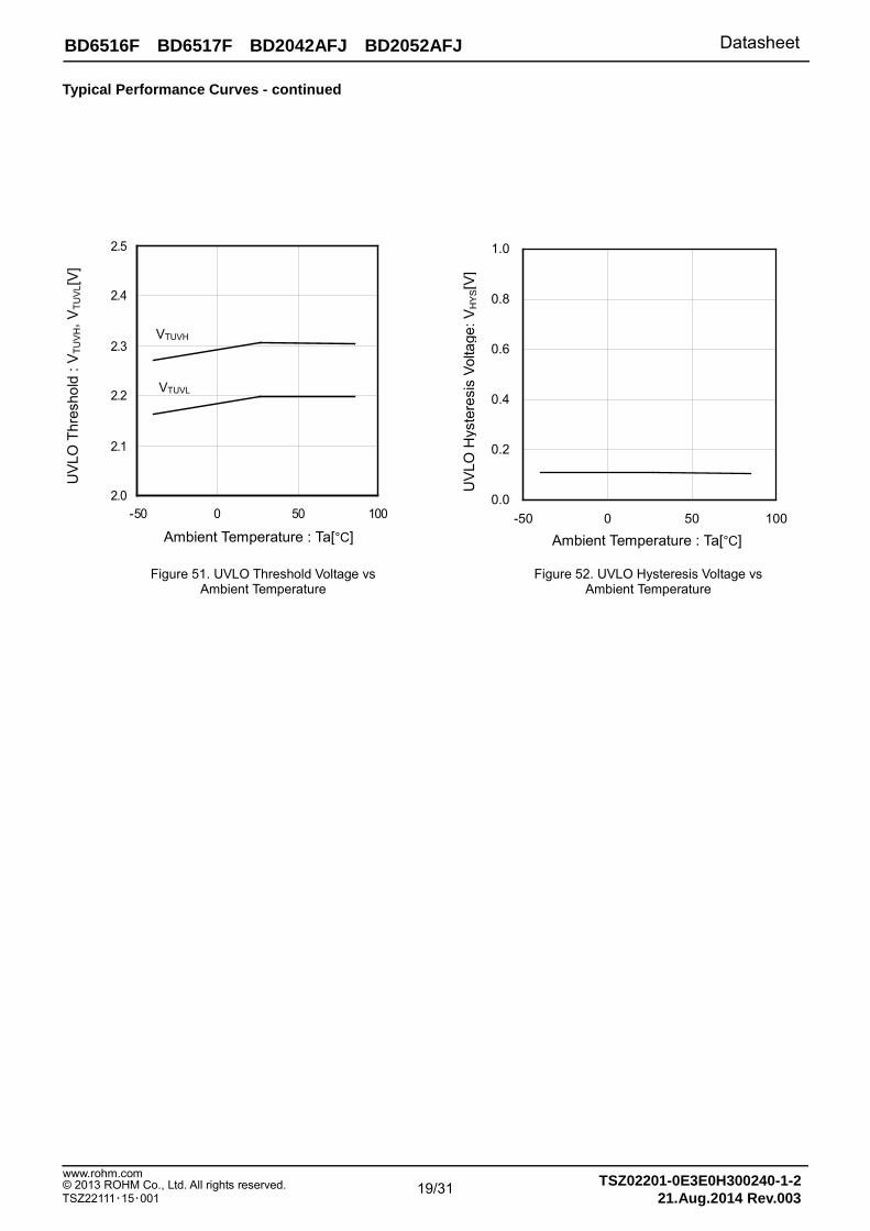
Figure 51. UVLO Threshold Voltage vs Ambient Temperature
2.0
2.1
2.2
2.3
2.4
2.5
-50 0 50 100AMBIENT TEMPERATURE : Ta[℃]
UVL
O T
HR
ESH
OLD
VO
LTAG
E : V
UVL
OH
,V
UVL
OL[V
]
VTUVH
VTUVL
UVL
O T
hres
hold
: V T
UV
H, V
TUV
L[V]
Ambient Temperature : Ta[°C]
0.0
0.2
0.4
0.6
0.8
1.0
-50 0 50 100
AMBIENT TEMPERATURE : Ta[℃]
Figure 52. UVLO Hysteresis Voltage vs Ambient Temperature
UVL
O H
yste
resi
s Vo
ltage
: VH
YS[V
]
Ambient Temperature : Ta[°C]
19/31 www.rohm.com © 2013 ROHM Co., Ltd. All rights reserved. TSZ22111・15・001
TSZ02201-0E3E0H300240-1-2 21.Aug.2014 Rev.003
BD6516F BD6517F BD2042AFJ BD2052AFJ Datasheet
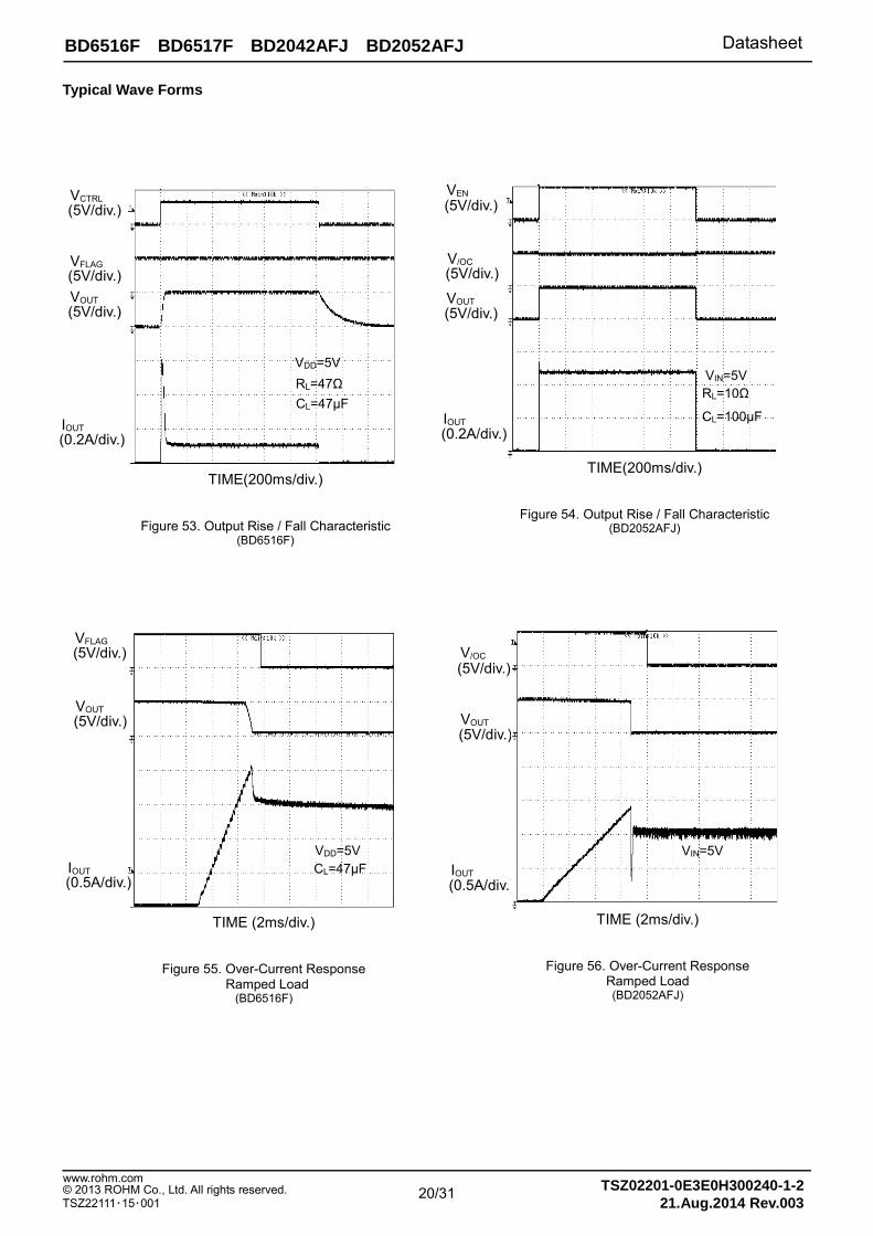
Typical Wave Forms
TIME(200ms/div.)
Figure 54. Output Rise / Fall Characteristic (BD2052AFJ)
VEN
(5V/div.)
V/OC
(5V/div.)
VOUT
(5V/div.)
IOUT (0.2A/div.)
VIN=5V RL=10Ω
CL=100μF
TIME(200ms/div.)
Figure 53. Output Rise / Fall Characteristic (BD6516F)
VCTRL
(5V/div.)
VFLAG (5V/div.) VOUT
(5V/div.)
IOUT
(0.2A/div.)
VDD=5V RL=47Ω CL=47μF
TIME (2ms/div.)
Figure 55. Over-Current Response Ramped Load
(BD6516F)
VDD=5V CL=47μF
VFLAG
(5V/div.)
VOUT
(5V/div.)
IOUT (0.5A/div.)
TIME (2ms/div.)
Figure 56. Over-Current Response Ramped Load (BD2052AFJ)
V/OC
(5V/div.)
VOUT
(5V/div.)
IOUT
(0.5A/div.)
VIN=5V
20/31 www.rohm.com © 2013 ROHM Co., Ltd. All rights reserved. TSZ22111・15・001
TSZ02201-0E3E0H300240-1-2 21.Aug.2014 Rev.003
BD6516F BD6517F BD2042AFJ BD2052AFJ Datasheet
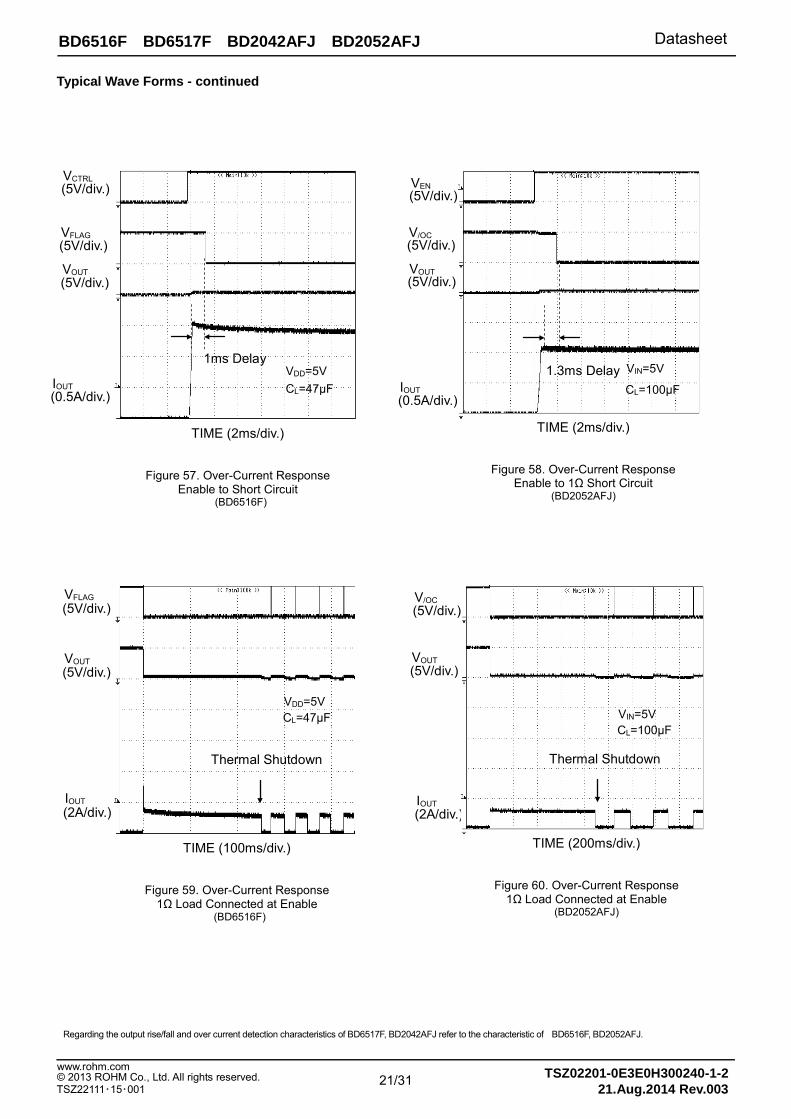
Typical Wave Forms - continued
Regarding the output rise/fall and over current detection characteristics of BD6517F, BD2042AFJ refer to the characteristic of BD6516F, BD2052AFJ.
VCTRL (5V/div.)
VFLAG (5V/div.)
VOUT (5V/div.)
IOUT (0.5A/div.)
VDD=5V CL=47μF
1ms Delay
TIME (2ms/div.)
Figure 57. Over-Current Response Enable to Short Circuit
(BD6516F)
V/OC (5V/div.)
VOUT
(5V/div.)
IOUT
(2A/div.)
VIN=5V CL=100μF
Thermal Shutdown
TIME (200ms/div.)
Figure 60. Over-Current Response 1Ω Load Connected at Enable
(BD2052AFJ)
TIME (2ms/div.)
Figure 58. Over-Current Response Enable to 1Ω Short Circuit
(BD2052AFJ)
VEN (5V/div.)
V/OC (5V/div.)
VOUT (5V/div.)
IOUT (0.5A/div.)
VIN=5V
CL=100μF 1.3ms Delay
TIME (100ms/div.)
Figure 59. Over-Current Response 1Ω Load Connected at Enable
(BD6516F)
VFLAG
(5V/div.)
VOUT
(5V/div.)
IOUT
(2A/div.)
Thermal Shutdown
VDD=5V CL=47μF
21/31 www.rohm.com © 2013 ROHM Co., Ltd. All rights reserved. TSZ22111・15・001
TSZ02201-0E3E0H300240-1-2 21.Aug.2014 Rev.003
BD6516F BD6517F BD2042AFJ BD2052AFJ Datasheet
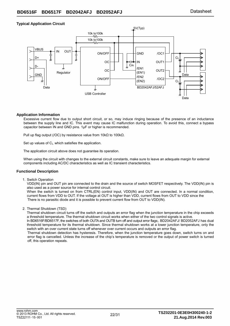
Typical Application Circuit
ON/OFF
OC
OC
ON/OFF
GND
IN
/EN1 (EN1)
/OC1
OUT1
OUT2
/OC2
10k to100k
5V(Typ)
OUT IN VBUS
D+
D-
GND
Data
Regulator
USB Controller
BD2042AFJ/52AFJ
CL
Data /EN2 (EN2)
10k to100k
CIN
Data
CL
Application Information
Excessive current flow due to output short circuit, or so, may induce ringing because of the presence of an inductance between the supply line and IC. This event may cause IC malfunction during operation. To avoid this, connect a bypass capacitor between IN and GND pins. 1μF or higher is recommended. Pull up flag output (/OC) by resistance value from 10kΩ to 100kΩ. Set up values of CL which satisfies the application. The application circuit above does not guarantee its operation. When using the circuit with changes to the external circuit constants, make sure to leave an adequate margin for external components including AC/DC characteristics as well as IC transient characteristics.
Functional Description
1. Switch Operation VDD(IN) pin and OUT pin are connected to the drain and the source of switch MOSFET respectively. The VDD(IN) pin is also used as a power source for internal control circuit. When the switch is turned on from CTRL(EN) control input, VDD(IN) and OUT are connected. In a normal condition, current flows from VDD to OUT. If the voltage at OUT is higher than VDD, current flows from OUT to VDD since the There is no parasitic diode and it is possible to prevent current flow from OUT to VDD(IN).
2. Thermal Shutdown (TSD)
Thermal shutdown circuit turns off the switch and outputs an error flag when the junction temperature in the chip exceeds a threshold temperature. The thermal shutdown circuit works when either of the two control signals is active. In BD6516F/BD6517F, the switches of both OUTA and OUTB turn off and output error flags;. BD2042AFJ/ BD2052AFJ has dual threshold temperature for its thermal shutdown. Since thermal shutdown works at a lower junction temperature, only the switch with an over current state turns off whenever over current occurs and outputs an error flag. Thermal shutdown detection has hysteresis. Therefore, when the junction temperature goes down, switch turns on and error flag is cancelled. Unless the increase of the chip’s temperature is removed or the output of power switch is turned off, this operation repeats.
22/31 www.rohm.com © 2013 ROHM Co., Ltd. All rights reserved. TSZ22111・15・001
TSZ02201-0E3E0H300240-1-2 21.Aug.2014 Rev.003
BD6516F BD6517F BD2042AFJ BD2052AFJ Datasheet
3. Over-Current Detection/Limit Circuit The over current detection circuit limits current (ISC) and outputs an error flag (/OC) when current flowing in each switch MOSFET exceeds a specified value. There are three types of response against over current. The over current detection circuit works when the switch is on (CTRL, EN signal is active).
(1) When the switch is turned on while the output is in short-circuit status, the switch goes into current limit status
immediately. (2) When the output short-circuits or high-current load is connected while the switch is on, very large current flows until
the over current limit circuit reacts. When the current detection and limit circuit works, current limitation is carried out. (3) When the output current increases gradually, current limitation does not work until the output current exceeds the
over current detection value. When it exceeds the detection value, current limitation is carried out.
4. Under Voltage Lockout (UVLO)
UVLO circuit turns off the switch to prevent malfunction when the supply voltage is below the UVLO threshold level, The UVLO circuit works when either of two control signals is active. ◎BD2042AFJ/BD2052AFJ
UVLO circuit prevents the switch from turning on until the VIN exceeds 2.3V(Typ). If the VIN drops below 2.2V(Typ) while the switch is ON, then UVLO shuts OFF the switch. UVLO has hysteresis of 100mV(Typ).
5. Error Flag (/OC) Output Error flag output is an N-MOS open drain output. At detection of over current limit and thermal shutdown, /OC outputs a low level signal. Error flag output (/OC) at over current detection has a delay filter. This delay filter prevents instantaneous current detection such as inrush current at switch ON, or applying external power supplies. If fault flag output is unused, /OC pin should be connected to open or ground line.
Output shortcircuit
Thermal shut down
VCTRL
VEN
VOUT
IOUT
VFLAG
V/OC
delay
Figure 61. BD6516F/ BD6517F/BD2042AFJ/ BD2052AFJ Over Current Detection, Thermal Shutdown Timing Diagram
(VCTRL, V/EN of BD6517F/BD2042AFJ Active Low)
VCTRL VOUT
IOUT VFLAG
Output Short Circuit
Thermal Shutdown
FLAG Output Delay
VCTRL VEN
VOUT
IOUT
VFLAG V/OC
23/31 www.rohm.com © 2013 ROHM Co., Ltd. All rights reserved. TSZ22111・15・001
TSZ02201-0E3E0H300240-1-2 21.Aug.2014 Rev.003
BD6516F BD6517F BD2042AFJ BD2052AFJ Datasheet
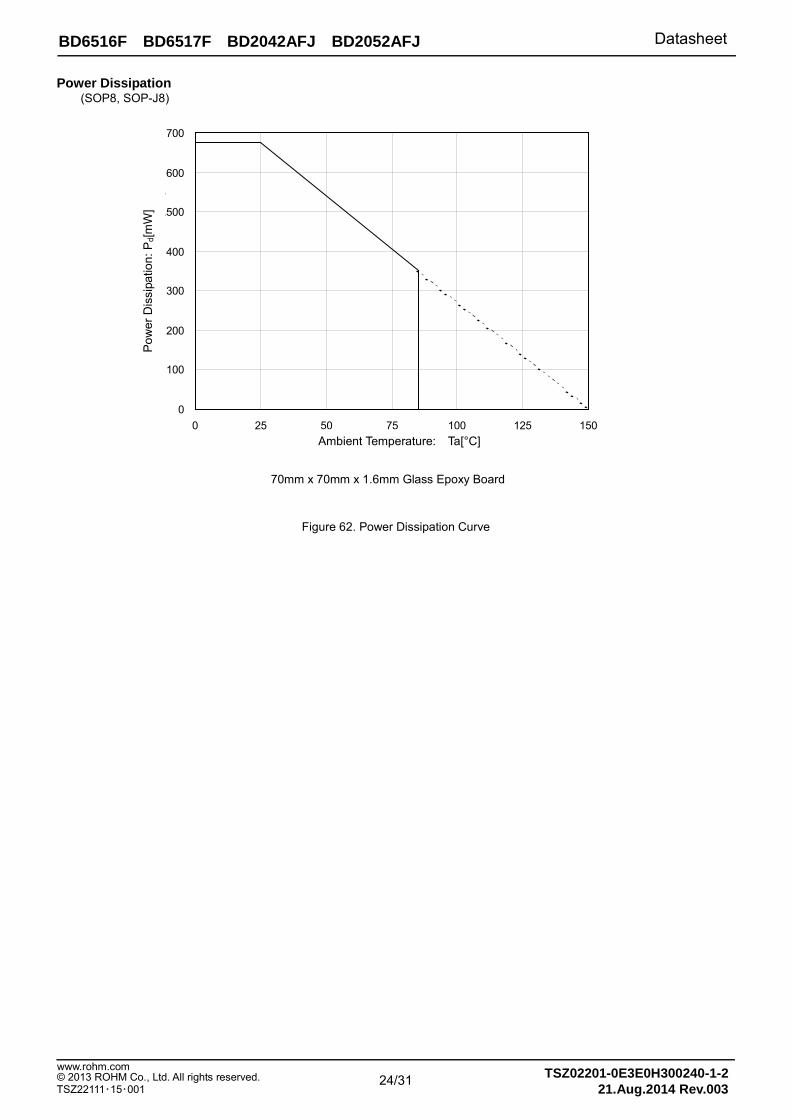
Power Dissipation (SOP8, SOP-J8)
Figure 62. Power Dissipation Curve
0
100
200
300
400
500
600
700
0 25 50 75 100 125 150AMBIENT TEMPERATURE : Ta [℃]
POW
ER D
ISSI
PATI
ON
: Pd
[mW
]P
ower
Dis
sipa
tion:
Pd[m
W]
Ambient Temperature: Ta[°C]
70mm x 70mm x 1.6mm Glass Epoxy Board
24/31 www.rohm.com © 2013 ROHM Co., Ltd. All rights reserved. TSZ22111・15・001
TSZ02201-0E3E0H300240-1-2 21.Aug.2014 Rev.003
BD6516F BD6517F BD2042AFJ BD2052AFJ Datasheet
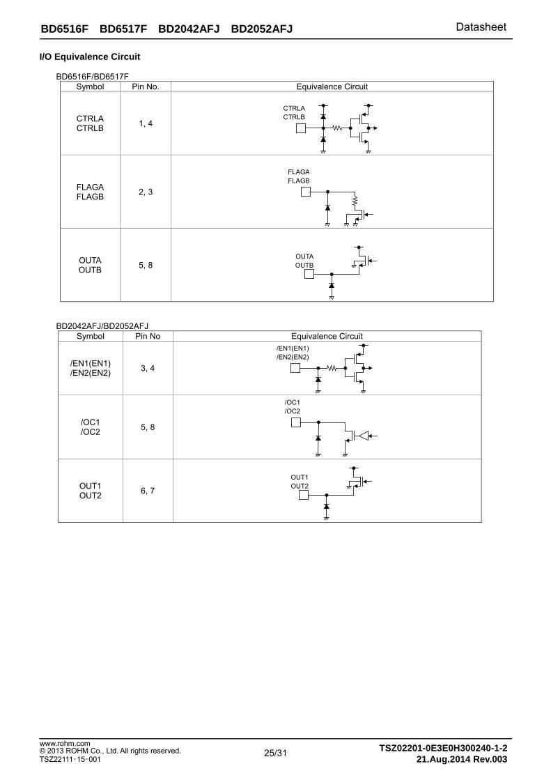
I/O Equivalence Circuit
BD6516F/BD6517F Symbol Pin No. Equivalence Circuit
CTRLA CTRLB 1, 4
CTRLA
CTRLB
FLAGA FLAGB 2, 3
FLAGA
FLAGB
OUTA OUTB 5, 8
OUTA OUTB
BD2042AFJ/BD2052AFJ Symbol Pin No Equivalence Circuit
/EN1(EN1) /EN2(EN2) 3, 4
/EN1(EN1) /EN2(EN2)
/OC1 /OC2 5, 8
/OC1 /OC2
OUT1 OUT2 6, 7
OUT1 OUT2
25/31 www.rohm.com © 2013 ROHM Co., Ltd. All rights reserved. TSZ22111・15・001
TSZ02201-0E3E0H300240-1-2 21.Aug.2014 Rev.003
BD6516F BD6517F BD2042AFJ BD2052AFJ Datasheet
Operational Notes 1. Reverse Connection of Power Supply
Connecting the power supply in reverse polarity can damage the IC. Take precautions against reverse polarity when connecting the power supply, such as mounting an external diode between the power supply and the IC’s power supply pins.
2. Power Supply Lines Design the PCB layout pattern to provide low impedance supply lines. Separate the ground and supply lines of the digital and analog blocks to prevent noise in the ground and supply lines of the digital block from affecting the analog block. Furthermore, connect a capacitor to ground at all power supply pins. Consider the effect of temperature and aging on the capacitance value when using electrolytic capacitors.
3. Ground Voltage Ensure that no pins are at a voltage below that of the ground pin at any time, even during transient condition.
4. Ground Wiring Pattern
When using both small-signal and large-current ground traces, the two ground traces should be routed separately but connected to a single ground at the reference point of the application board to avoid fluctuations in the small-signal ground caused by large currents. Also ensure that the ground traces of external components do not cause variations on the ground voltage. The ground lines must be as short and thick as possible to reduce line impedance.
5. Thermal Consideration
Should by any chance the power dissipation rating be exceeded the rise in temperature of the chip may result in deterioration of the properties of the chip. The absolute maximum rating of the Pd stated in this specification is when the IC is mounted on a 70mm x 70mm x 1.6mm glass epoxy board. In case of exceeding this absolute maximum rating, increase the board size and copper area to prevent exceeding the Pd rating.
6. Recommended Operating Conditions
These conditions represent a range within which the expected characteristics of the IC can be approximately obtained. The electrical characteristics are guaranteed under the conditions of each parameter.
7. In rush Current
When power is first supplied to the IC, it is possible that the internal logic may be unstable and inrush current may flow instantaneously due to the internal powering sequence and delays, especially if the IC has more than one power supply. Therefore, give special consideration to power coupling capacitance, power wiring, width of ground wiring, and routing of connections.
8. Operation Under Strong Electromagnetic Field
Operating the IC in the presence of a strong electromagnetic field may cause the IC to malfunction.
9. Testing on Application Boards When testing the IC on an application board, connecting a capacitor directly to a low-impedance output pin may subject the IC to stress. Always discharge capacitors completely after each process or step. The IC’s power supply should always be turned off completely before connecting or removing it from the test setup during the inspection process. To prevent damage from static discharge, ground the IC during assembly and use similar precautions during transport and storage.
10. Inter-pin Short and Mounting Errors Ensure that the direction and position are correct when mounting the IC on the PCB. Incorrect mounting may result in damaging the IC. Avoid nearby pins being shorted to each other especially to ground, power supply and output pin. Inter-pin shorts could be due to many reasons such as metal particles, water droplets (in very humid environment) and unintentional solder bridge deposited in between pins during assembly to name a few.
26/31 www.rohm.com © 2013 ROHM Co., Ltd. All rights reserved. TSZ22111・15・001
TSZ02201-0E3E0H300240-1-2 21.Aug.2014 Rev.003
BD6516F BD6517F BD2042AFJ BD2052AFJ Datasheet
Operational Notes - continued 11. Unused Input Pins
Input pins of an IC are often connected to the gate of a MOS transistor. The gate has extremely high impedance and extremely low capacitance. If left unconnected, the electric field from the outside can easily charge it. The small charge acquired in this way is enough to produce a significant effect on the conduction through the transistor and cause unexpected operation of the IC. So unless otherwise specified, unused input pins should be connected to the power supply or ground line.
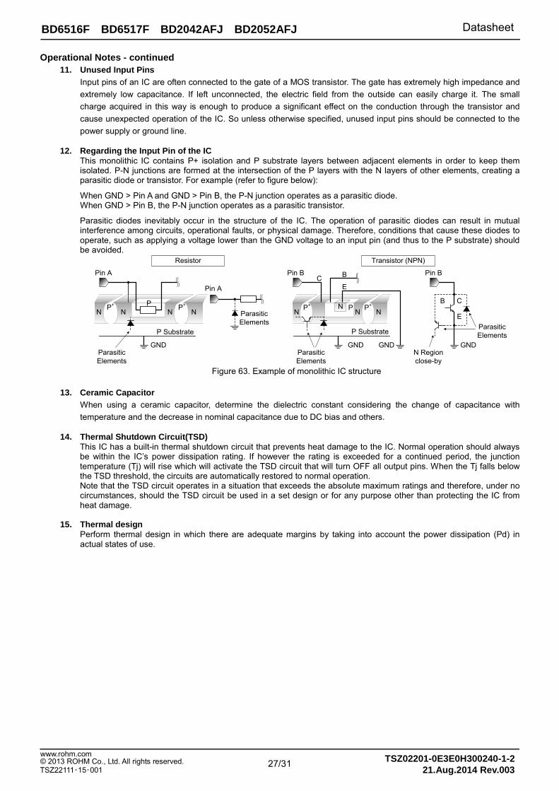
12. Regarding the Input Pin of the IC
This monolithic IC contains P+ isolation and P substrate layers between adjacent elements in order to keep them isolated. P-N junctions are formed at the intersection of the P layers with the N layers of other elements, creating a parasitic diode or transistor. For example (refer to figure below):
When GND > Pin A and GND > Pin B, the P-N junction operates as a parasitic diode. When GND > Pin B, the P-N junction operates as a parasitic transistor.
Parasitic diodes inevitably occur in the structure of the IC. The operation of parasitic diodes can result in mutual interference among circuits, operational faults, or physical damage. Therefore, conditions that cause these diodes to operate, such as applying a voltage lower than the GND voltage to an input pin (and thus to the P substrate) should be avoided.
Figure 63. Example of monolithic IC structure
13. Ceramic Capacitor When using a ceramic capacitor, determine the dielectric constant considering the change of capacitance with temperature and the decrease in nominal capacitance due to DC bias and others.
14. Thermal Shutdown Circuit(TSD)
This IC has a built-in thermal shutdown circuit that prevents heat damage to the IC. Normal operation should always be within the IC’s power dissipation rating. If however the rating is exceeded for a continued period, the junction temperature (Tj) will rise which will activate the TSD circuit that will turn OFF all output pins. When the Tj falls below the TSD threshold, the circuits are automatically restored to normal operation. Note that the TSD circuit operates in a situation that exceeds the absolute maximum ratings and therefore, under no circumstances, should the TSD circuit be used in a set design or for any purpose other than protecting the IC from heat damage.
15. Thermal design
Perform thermal design in which there are adequate margins by taking into account the power dissipation (Pd) in actual states of use.
N NP+ P
N NP+
P Substrate
GND
N P+
N NP+N P
P Substrate
GND GND
Parasitic Elements
Pin A
Pin A
Pin B Pin B
B C
EParasitic Elements
GNDParasitic Elements
C B
E
Transistor (NPN)Resistor
N Regionclose-by
Parasitic Elements
27/31 www.rohm.com © 2013 ROHM Co., Ltd. All rights reserved. TSZ22111・15・001
TSZ02201-0E3E0H300240-1-2 21.Aug.2014 Rev.003
BD6516F BD6517F BD2042AFJ BD2052AFJ Datasheet
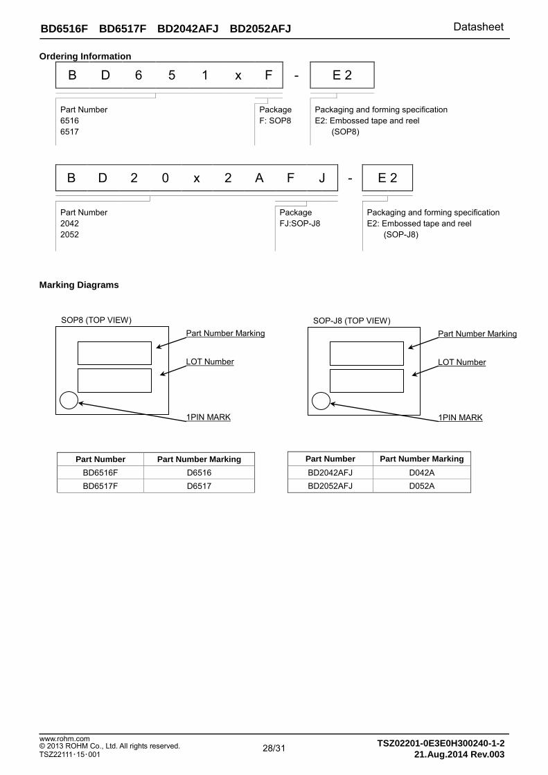
Ordering Information
B D 6 5 1 x F - E 2 Part Number 6516 6517
Package F: SOP8
Packaging and forming specification E2: Embossed tape and reel (SOP8)
B D 2 0 x 2 A F J - E 2 Part Number 2042 2052
Package FJ:SOP-J8
Packaging and forming specification E2: Embossed tape and reel (SOP-J8)
Marking Diagrams
Part Number Part Number Marking BD6516F D6516 BD6517F D6517
Part Number Part Number Marking BD2042AFJ D042A BD2052AFJ D052A
SOP8 (TOP VIEW)
Part Number Marking
LOT Number
1PIN MARK
SOP-J8 (TOP VIEW)
Part Number Marking
LOT Number
1PIN MARK
28/31 www.rohm.com © 2013 ROHM Co., Ltd. All rights reserved. TSZ22111・15・001
TSZ02201-0E3E0H300240-1-2 21.Aug.2014 Rev.003
BD6516F BD6517F BD2042AFJ BD2052AFJ Datasheet
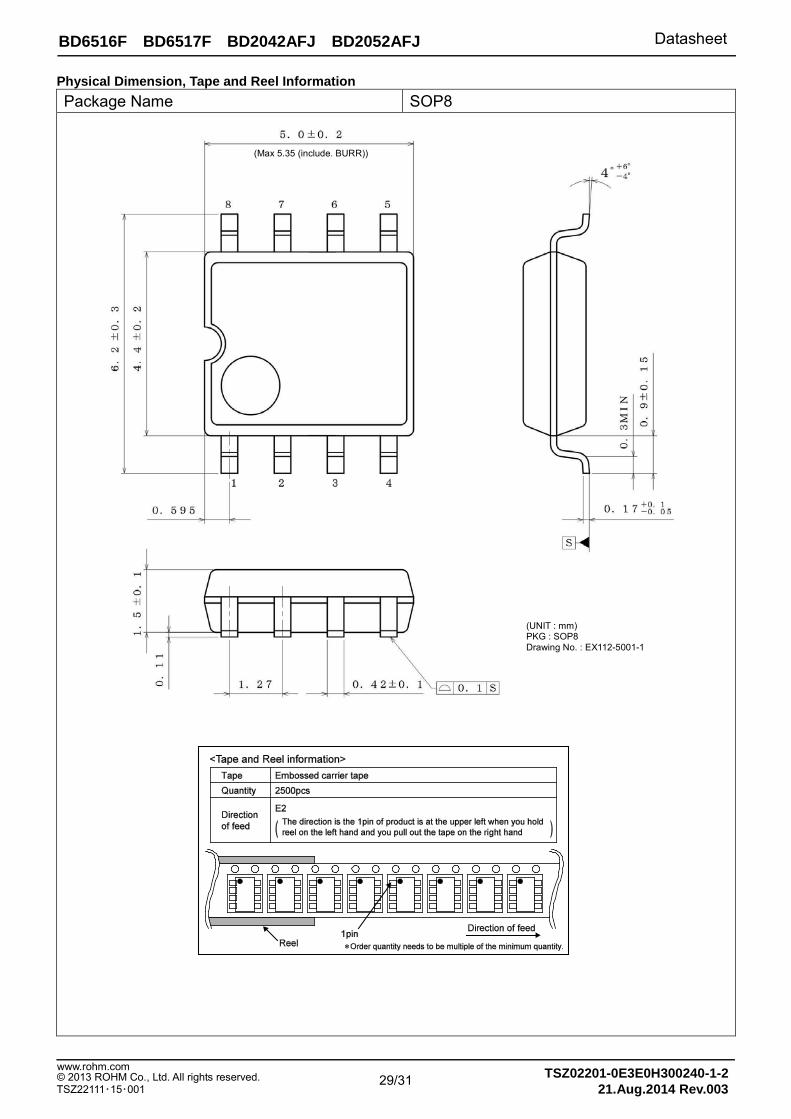
Physical Dimension, Tape and Reel Information Package Name SOP8
(UNIT : mm) PKG : SOP8 Drawing No. : EX112-5001-1
(Max 5.35 (include. BURR))
29/31 www.rohm.com © 2013 ROHM Co., Ltd. All rights reserved. TSZ22111・15・001
TSZ02201-0E3E0H300240-1-2 21.Aug.2014 Rev.003
BD6516F BD6517F BD2042AFJ BD2052AFJ Datasheet
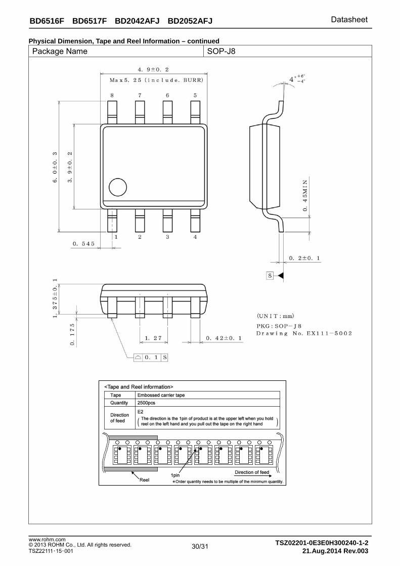
Physical Dimension, Tape and Reel Information – continued Package Name SOP-J8
30/31 www.rohm.com © 2013 ROHM Co., Ltd. All rights reserved. TSZ22111・15・001
TSZ02201-0E3E0H300240-1-2 21.Aug.2014 Rev.003
BD6516F BD6517F BD2042AFJ BD2052AFJ Datasheet
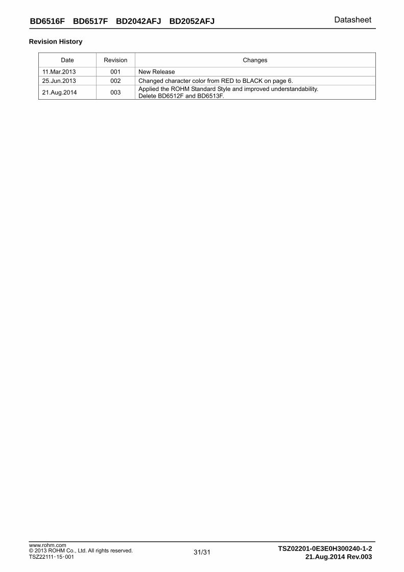
Revision History
Date Revision Changes
11.Mar.2013 001 New Release 25.Jun.2013 002 Changed character color from RED to BLACK on page 6.
21.Aug.2014 003 Applied the ROHM Standard Style and improved understandability. Delete BD6512F and BD6513F.
31/31 www.rohm.com © 2013 ROHM Co., Ltd. All rights reserved. TSZ22111・15・001
TSZ02201-0E3E0H300240-1-2 21.Aug.2014 Rev.003
DatasheetDatasheet
Notice – GE Rev.002© 2013 ROHM Co., Ltd. All rights reserved.
Notice Precaution on using ROHM Products
1. Our Products are designed and manufactured for application in ordinary electronic equipments (such as AV equipment, OA equipment, telecommunication equipment, home electronic appliances, amusement equipment, etc.). If you intend to use our Products in devices requiring extremely high reliability (such as medical equipment (Note 1), transport equipment, traffic equipment, aircraft/spacecraft, nuclear power controllers, fuel controllers, car equipment including car accessories, safety devices, etc.) and whose malfunction or failure may cause loss of human life, bodily injury or serious damage to property (“Specific Applications”), please consult with the ROHM sales representative in advance. Unless otherwise agreed in writing by ROHM in advance, ROHM shall not be in any way responsible or liable for any damages, expenses or losses incurred by you or third parties arising from the use of any ROHM’s Products for Specific Applications.
(Note1) Medical Equipment Classification of the Specific Applications JAPAN USA EU CHINA
CLASSⅢ CLASSⅢ
CLASSⅡb CLASSⅢ
CLASSⅣ CLASSⅢ
2. ROHM designs and manufactures its Products subject to strict quality control system. However, semiconductor products can fail or malfunction at a certain rate. Please be sure to implement, at your own responsibilities, adequate safety measures including but not limited to fail-safe design against the physical injury, damage to any property, which a failure or malfunction of our Products may cause. The following are examples of safety measures:
[a] Installation of protection circuits or other protective devices to improve system safety [b] Installation of redundant circuits to reduce the impact of single or multiple circuit failure
3. Our Products are designed and manufactured for use under standard conditions and not under any special or extraordinary environments or conditions, as exemplified below. Accordingly, ROHM shall not be in any way responsible or liable for any damages, expenses or losses arising from the use of any ROHM’s Products under any special or extraordinary environments or conditions. If you intend to use our Products under any special or extraordinary environments or conditions (as exemplified below), your independent verification and confirmation of product performance, reliability, etc, prior to use, must be necessary:
[a] Use of our Products in any types of liquid, including water, oils, chemicals, and organic solvents [b] Use of our Products outdoors or in places where the Products are exposed to direct sunlight or dust [c] Use of our Products in places where the Products are exposed to sea wind or corrosive gases, including Cl2,
H2S, NH3, SO2, and NO2 [d] Use of our Products in places where the Products are exposed to static electricity or electromagnetic waves [e] Use of our Products in proximity to heat-producing components, plastic cords, or other flammable items [f] Sealing or coating our Products with resin or other coating materials [g] Use of our Products without cleaning residue of flux (even if you use no-clean type fluxes, cleaning residue of
flux is recommended); or Washing our Products by using water or water-soluble cleaning agents for cleaning residue after soldering
[h] Use of the Products in places subject to dew condensation
4. The Products are not subject to radiation-proof design. 5. Please verify and confirm characteristics of the final or mounted products in using the Products. 6. In particular, if a transient load (a large amount of load applied in a short period of time, such as pulse. is applied,
confirmation of performance characteristics after on-board mounting is strongly recommended. Avoid applying power exceeding normal rated power; exceeding the power rating under steady-state loading condition may negatively affect product performance and reliability.
7. De-rate Power Dissipation (Pd) depending on Ambient temperature (Ta). When used in sealed area, confirm the actual
ambient temperature. 8. Confirm that operation temperature is within the specified range described in the product specification. 9. ROHM shall not be in any way responsible or liable for failure induced under deviant condition from what is defined in
this document.
Precaution for Mounting / Circuit board design 1. When a highly active halogenous (chlorine, bromine, etc.) flux is used, the residue of flux may negatively affect product
performance and reliability. 2. In principle, the reflow soldering method must be used; if flow soldering method is preferred, please consult with the
ROHM representative in advance. For details, please refer to ROHM Mounting specification
DatasheetDatasheet
Notice – GE Rev.002© 2013 ROHM Co., Ltd. All rights reserved.
Precautions Regarding Application Examples and External Circuits 1. If change is made to the constant of an external circuit, please allow a sufficient margin considering variations of the
characteristics of the Products and external components, including transient characteristics, as well as static characteristics.
2. You agree that application notes, reference designs, and associated data and information contained in this document
are presented only as guidance for Products use. Therefore, in case you use such information, you are solely responsible for it and you must exercise your own independent verification and judgment in the use of such information contained in this document. ROHM shall not be in any way responsible or liable for any damages, expenses or losses incurred by you or third parties arising from the use of such information.
Precaution for Electrostatic
This Product is electrostatic sensitive product, which may be damaged due to electrostatic discharge. Please take proper caution in your manufacturing process and storage so that voltage exceeding the Products maximum rating will not be applied to Products. Please take special care under dry condition (e.g. Grounding of human body / equipment / solder iron, isolation from charged objects, setting of Ionizer, friction prevention and temperature / humidity control).
Precaution for Storage / Transportation 1. Product performance and soldered connections may deteriorate if the Products are stored in the places where:
[a] the Products are exposed to sea winds or corrosive gases, including Cl2, H2S, NH3, SO2, and NO2 [b] the temperature or humidity exceeds those recommended by ROHM [c] the Products are exposed to direct sunshine or condensation [d] the Products are exposed to high Electrostatic
2. Even under ROHM recommended storage condition, solderability of products out of recommended storage time period may be degraded. It is strongly recommended to confirm solderability before using Products of which storage time is exceeding the recommended storage time period.
3. Store / transport cartons in the correct direction, which is indicated on a carton with a symbol. Otherwise bent leads
may occur due to excessive stress applied when dropping of a carton. 4. Use Products within the specified time after opening a humidity barrier bag. Baking is required before using Products of
which storage time is exceeding the recommended storage time period.
Precaution for Product Label QR code printed on ROHM Products label is for ROHM’s internal use only.
Precaution for Disposition When disposing Products please dispose them properly using an authorized industry waste company.
Precaution for Foreign Exchange and Foreign Trade act Since our Products might fall under controlled goods prescribed by the applicable foreign exchange and foreign trade act, please consult with ROHM representative in case of export.
Precaution Regarding Intellectual Property Rights 1. All information and data including but not limited to application example contained in this document is for reference
only. ROHM does not warrant that foregoing information or data will not infringe any intellectual property rights or any other rights of any third party regarding such information or data. ROHM shall not be in any way responsible or liable for infringement of any intellectual property rights or other damages arising from use of such information or data.:
2. No license, expressly or implied, is granted hereby under any intellectual property rights or other rights of ROHM or any
third parties with respect to the information contained in this document.
Other Precaution 1. This document may not be reprinted or reproduced, in whole or in part, without prior written consent of ROHM. 2. The Products may not be disassembled, converted, modified, reproduced or otherwise changed without prior written
consent of ROHM. 3. In no event shall you use in any way whatsoever the Products and the related technical information contained in the
Products or this document for any military purposes, including but not limited to, the development of mass-destruction weapons.
4. The proper names of companies or products described in this document are trademarks or registered trademarks of
ROHM, its affiliated companies or third parties.

DatasheetDatasheet
Notice – WE Rev.001© 2014 ROHM Co., Ltd. All rights reserved.
General Precaution 1. Before you use our Pro ducts, you are requested to care fully read this document and fully understand its contents.
ROHM shall n ot be in an y way responsible or liabl e for fa ilure, malfunction or acci dent arising from the use of a ny ROHM’s Products against warning, caution or note contained in this document.
2. All information contained in this docume nt is current as of the issuing date and subj ect to change without any prior
notice. Before purchasing or using ROHM’s Products, please confirm the la test information with a ROHM sale s representative.
3. The information contained in this doc ument is provi ded on an “as is” basis and ROHM does not warrant that all
information contained in this document is accurate an d/or error-free. ROHM shall not be in an y way responsible or liable for any damages, expenses or losses incurred by you or third parties resulting from inaccuracy or errors of or concerning such information.