16Bit ΔΣ CODEC with MIC/HP/SPK-AMP & TSC - akm.com · PDF fileRecording Function...
86
[AK4650] MS0502-E-01 2007/04 - 1 - GENERAL DESCRIPTION The AK4650 targeted at PDA and other low-power, small size applications. It features a 16bit stereo CODEC with a built-in Microphone-Amplifier, Headphone-Amplifier, Speaker-Amplifier and Touch Screen Controller. Input circuits include a Microphone-Amplifier and an ALC (Auto Level Control) circuit. The AK4650 is connected with AC’97 controller (CPU) via AC-Link. The AK4650 is available in a very small 57pin BGA, utilizing less board space than competitive offerings. FEATURES 1. Resolution: 16bits 2. Recording Function • Mono Input (Single-ended or Differential Input) • 2 to 1 Selector (Internal and External MIC) • MIC Power: 2 outputs (Internal and External MIC) • 1 st MIC Amplifier: +20dB or 0dB • 2 nd Amplifier with ALC: +27.5dB ∼ −8dB, 0.5dB Step • ADC Performance (@MIC-Amp=+20dB, Single-ended): S/(N+D): 79dB, DR, S/N: 83dB • MIC Detection 3. Playback Function • Digital De-emphasis Filter (tc=50/15μs, fs=32kHz, 44.1kHz, 48kHz) • Digital Volume (0dB ∼ −63dB, 0.5dB Step, Mute) • Bass Boost • Mono Output - Full-differential Output - S/(N+D): 85dB, S/N: 95dB - Analog Volume: +6dB ∼ −15dB, 3dB Step • Headphone-Amp - Output Power: 40mW@16Ω (HVDD=3.3V) - S/(N+D): 60dB@10mW, S/N: 90dB • Headphone Jack Detection • Mono Speaker-Amp - Output Power: 300mW@8Ω (HVDD=3.3V, ALC2=OFF) - S/(N+D): 55dB@110mW, S/N: 90dB - BTL Output - ALC (Auto Level Control) circuit • Mono Beep Input • AUX Input - Full-differential Input - Analog Volume: +12dB ∼ −34.5dB, 1.5dB Step, Mute • Stereo Line Input - Single-ended Input - Analog Volume: +12dB ∼ −34.5dB, 1.5dB Step, Mute 16Bit ΔΣ CODEC with MIC/HP/SPK-AMP & TSC AK4650
-
Upload
duongduong -
Category
Documents
-
view
215 -
download
1
Transcript of 16Bit ΔΣ CODEC with MIC/HP/SPK-AMP & TSC - akm.com · PDF fileRecording Function...
[AK4650]
MS0502-E-01 2007/04 - 1 -
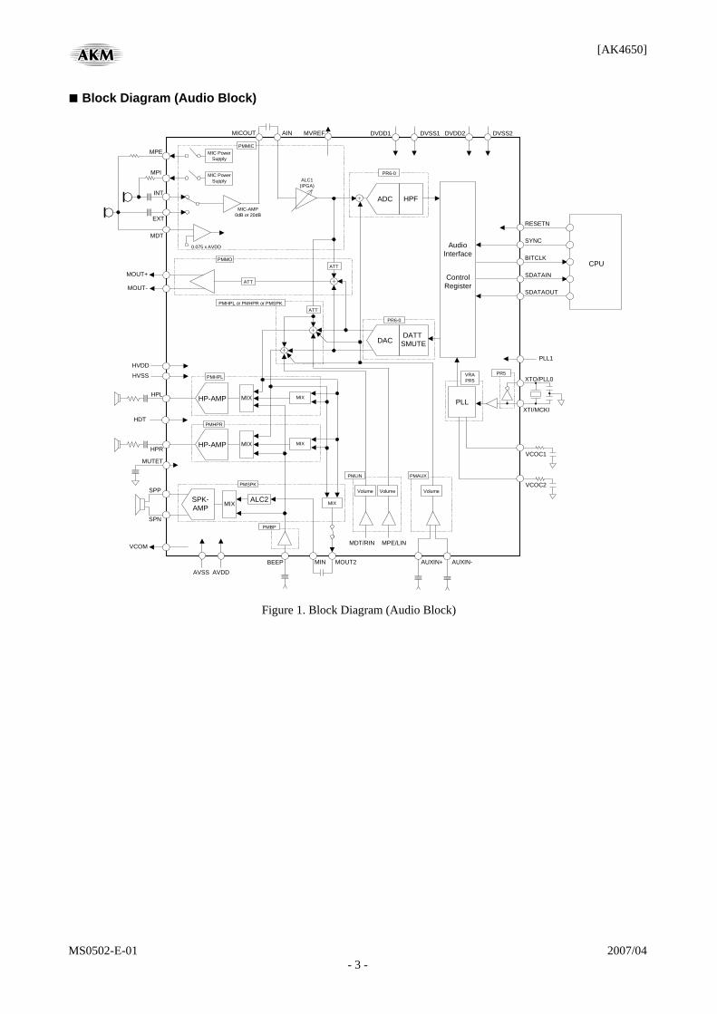
GENERAL DESCRIPTION The AK4650 targeted at PDA and other low-power, small size applications. It features a 16bit stereo CODEC with a built-in Microphone-Amplifier, Headphone-Amplifier, Speaker-Amplifier and Touch Screen Controller. Input circuits include a Microphone-Amplifier and an ALC (Auto Level Control) circuit. The AK4650 is connected with AC’97 controller (CPU) via AC-Link. The AK4650 is available in a very small 57pin BGA, utilizing less board space than competitive offerings.
FEATURES 1. Resolution: 16bits 2. Recording Function
• Mono Input (Single-ended or Differential Input) • 2 to 1 Selector (Internal and External MIC) • MIC Power: 2 outputs (Internal and External MIC) • 1st MIC Amplifier: +20dB or 0dB • 2nd Amplifier with ALC: +27.5dB ∼ −8dB, 0.5dB Step • ADC Performance (@MIC-Amp=+20dB, Single-ended):
S/(N+D): 79dB, DR, S/N: 83dB • MIC Detection
3. Playback Function • Digital De-emphasis Filter (tc=50/15μs, fs=32kHz, 44.1kHz, 48kHz) • Digital Volume (0dB ∼ −63dB, 0.5dB Step, Mute) • Bass Boost • Mono Output
- Full-differential Output - S/(N+D): 85dB, S/N: 95dB - Analog Volume: +6dB ∼ −15dB, 3dB Step
• Headphone-Amp - Output Power: 40mW@16Ω (HVDD=3.3V) - S/(N+D): 60dB@10mW, S/N: 90dB
• Headphone Jack Detection • Mono Speaker-Amp
- Output Power: 300mW@8Ω (HVDD=3.3V, ALC2=OFF) - S/(N+D): 55dB@110mW, S/N: 90dB - BTL Output - ALC (Auto Level Control) circuit
• Mono Beep Input • AUX Input
- Full-differential Input - Analog Volume: +12dB ∼ −34.5dB, 1.5dB Step, Mute
• Stereo Line Input - Single-ended Input - Analog Volume: +12dB ∼ −34.5dB, 1.5dB Step, Mute
16Bit ΔΣ CODEC with MIC/HP/SPK-AMP & TSC
AK4650

[AK4650]
MS0502-E-01 2007/04 - 2 -
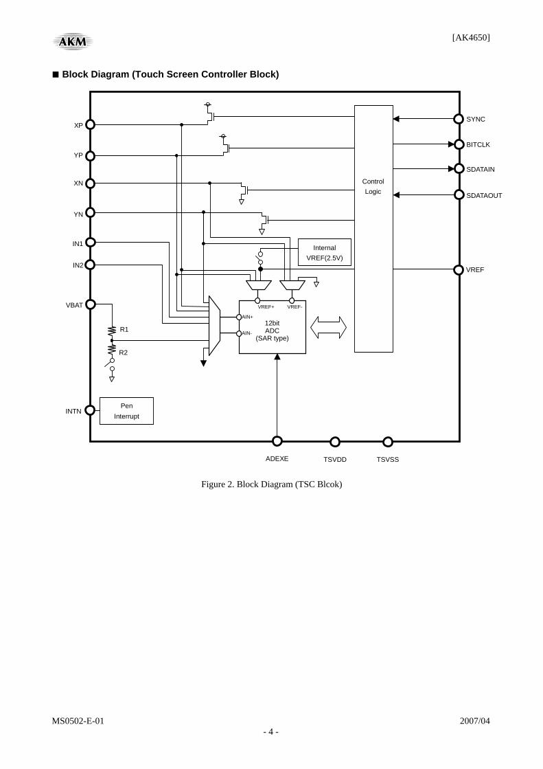
4. Touch Screen Controller • Two Auxiliary Analog Inputs • Pen Pressure Measurement • Direct Battery Measurement • On-Chip Voltage Reference (2.5V) • 12 bit SAR type A/D Converter
5. System Clock: 24.576MHz, 12MHz, 3.6864MHz 6. Sampling Rate: 48kHz, 44.1kHz, 32kHz, 24kHz, 22.05kHz, 16kHz, 11.025kHz, 8kHz 7. Power Management 8. Audio, Touch Screen & Control I/F: AC-Link I/F 9. Ta = −30 ∼ 85°C 10. Power Supply: 2.7V ∼ 3.6V (typ. 3.3V) 11. Package: 57pin BGA (5mm x 5mm)
[AK4650]
MS0502-E-01 2007/04 - 3 -
■ Block Diagram (Audio Block)
ALC1(IPGA)
PMMIC
ATT
MICOUT AIN
SYNC
BITCLK
SDATAIN
SDATAOUT
RESETN
CPU
AVDDAVSS
HVDD
HVSS
VCOM
MUTET
MIN MOUT2 AUXIN+
MIX
HPL
PMHPL
HP-AMP
HPR
PMHPR
HP-AMP
AudioInterface
PMSPK
SPK-AMP
SPP
SPN
Volume
PMMO
PMHPL or PMHPR or PMSPK
MOUT+ATT
PLLXTI/MCKI
XTO/PLL0
VCOC1
VRAPR5
MIX
MIX
MIX MIX
PMAUX
MPE MIC PowerSupply
MDT
0.075 x AVDD
EXT
INT
MIC-AMP0dB or 20dB
MPI MIC PowerSupply
HPFADC
PR6-0
PR6-0
DATTSMUTEDAC
MIX
ATT
ALC2
ControlRegister
HDT
VolumeVolume
MPE/LINMDT/RIN
DVDD2 DVSS2
AUXIN-
MOUT-
BEEP
PMLIN
PMBP
PR5
MVREF
VCOC2
PLL1
DVDD1 DVSS1
Figure 1. Block Diagram (Audio Block)
[AK4650]
MS0502-E-01 2007/04 - 4 -
■ Block Diagram (Touch Screen Controller Block)
YN
XN
YP
XP
12bit ADC
(SAR type)
VBAT VREF+
AIN+
VREF
SYNC
BITCLK
SDATAIN
SDATAOUT
IN1
INTN
TSVDD TSVSS
Internal VREF(2.5V)
VREF-
Control Logic
IN2
R1
R2
AIN-
Pen Interrupt
ADEXE
Figure 2. Block Diagram (TSC Blcok)
[AK4650]
MS0502-E-01 2007/04 - 5 -
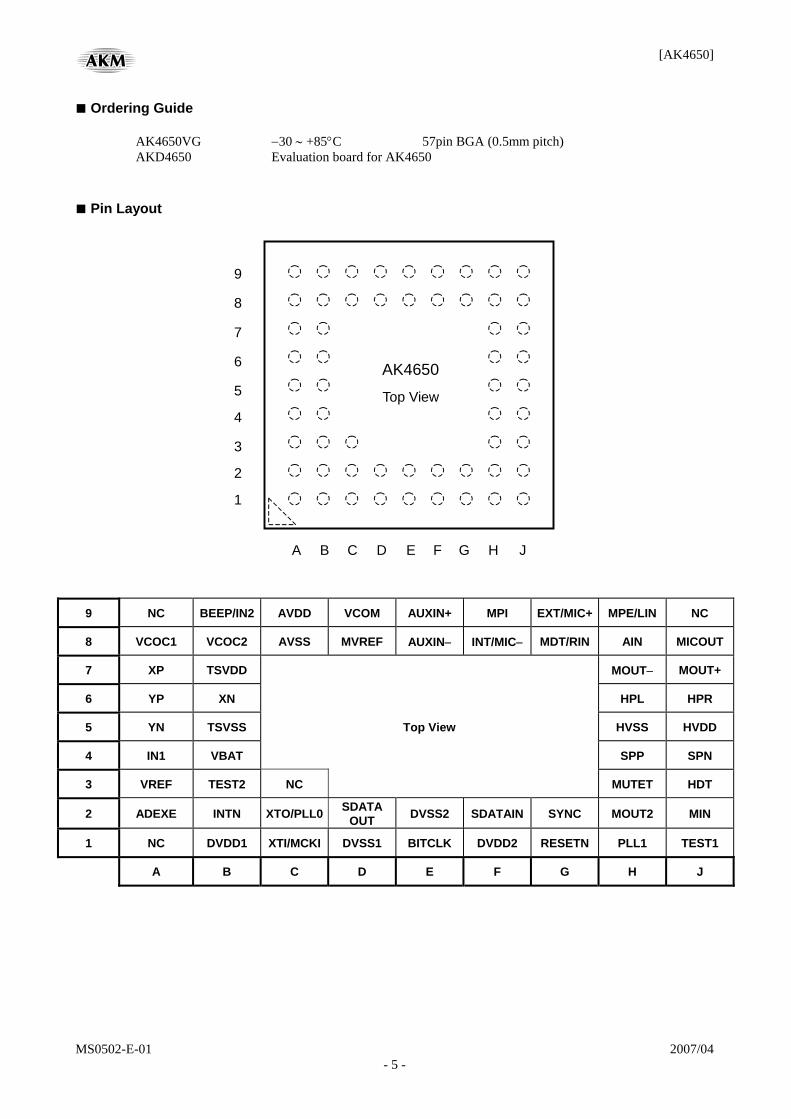
■ Ordering Guide AK4650VG −30 ∼ +85°C 57pin BGA (0.5mm pitch) AKD4650 Evaluation board for AK4650 ■ Pin Layout
A
Top View
B C ED F G H J
6
7
8
9
5
3
4
1
2
AK4650
9 NC BEEP/IN2 AVDD VCOM AUXIN+ MPI EXT/MIC+ MPE/LIN NC
8 VCOC1 VCOC2 AVSS MVREF AUXIN− INT/MIC− MDT/RIN AIN MICOUT
7 XP TSVDD MOUT− MOUT+
6 YP XN HPL HPR
5 YN TSVSS Top View HVSS HVDD
4 IN1 VBAT SPP SPN
3 VREF TEST2 NC MUTET HDT
2 ADEXE INTN XTO/PLL0 SDATA OUT DVSS2 SDATAIN SYNC MOUT2 MIN
1 NC DVDD1 XTI/MCKI DVSS1 BITCLK DVDD2 RESETN PLL1 TEST1
A B C D E F G H J
[AK4650]
MS0502-E-01 2007/04 - 6 -
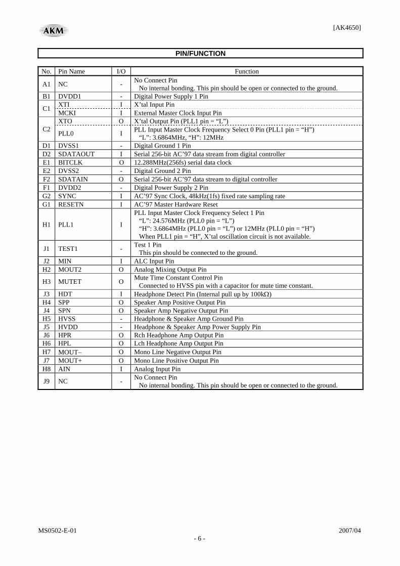
PIN/FUNCTION
No. Pin Name I/O Function
A1 NC - No Connect Pin No internal bonding. This pin should be open or connected to the ground.
B1 DVDD1 - Digital Power Supply 1 Pin XTI I X’tal Input Pin C1 MCKI I External Master Clock Input Pin XTO O X’tal Output Pin (PLL1 pin = “L”)
C2 PLL0 I PLL Input Master Clock Frequency Select 0 Pin (PLL1 pin = “H”) “L”: 3.6864MHz, “H”: 12MHz
D1 DVSS1 - Digital Ground 1 Pin D2 SDATAOUT I Serial 256-bit AC’97 data stream from digital controller E1 BITCLK O 12.288MHz(256fs) serial data clock E2 DVSS2 - Digital Ground 2 Pin F2 SDATAIN O Serial 256-bit AC’97 data stream to digital controller F1 DVDD2 - Digital Power Supply 2 Pin G2 SYNC I AC’97 Sync Clock, 48kHz(1fs) fixed rate sampling rate G1 RESETN I AC’97 Master Hardware Reset
H1 PLL1 I
PLL Input Master Clock Frequency Select 1 Pin “L”: 24.576MHz (PLL0 pin = “L”) “H”: 3.6864MHz (PLL0 pin = “L”) or 12MHz (PLL0 pin = “H”) When PLL1 pin = “H”, X’tal oscillation circuit is not available.
J1 TEST1 - Test 1 Pin This pin should be connected to the ground.
J2 MIN I ALC Input Pin H2 MOUT2 O Analog Mixing Output Pin
H3 MUTET O Mute Time Constant Control Pin Connected to HVSS pin with a capacitor for mute time constant.
J3 HDT I Headphone Detect Pin (Internal pull up by 100kΩ) H4 SPP O Speaker Amp Positive Output Pin J4 SPN O Speaker Amp Negative Output Pin H5 HVSS - Headphone & Speaker Amp Ground Pin J5 HVDD - Headphone & Speaker Amp Power Supply Pin J6 HPR O Rch Headphone Amp Output Pin H6 HPL O Lch Headphone Amp Output Pin H7 MOUT− O Mono Line Negative Output Pin J7 MOUT+ O Mono Line Positive Output Pin H8 AIN I Analog Input Pin
J9 NC - No Connect Pin No internal bonding. This pin should be open or connected to the ground.
[AK4650]
MS0502-E-01 2007/04 - 7 -
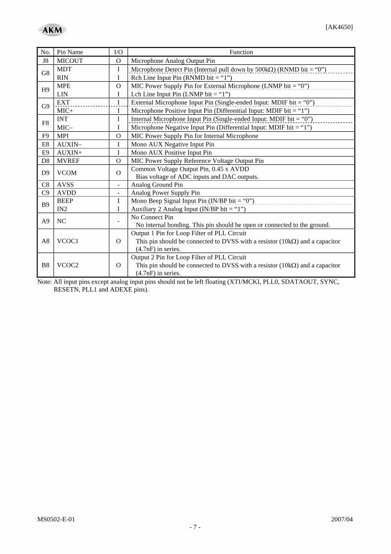
No. Pin Name I/O Function J8 MICOUT O Microphone Analog Output Pin
MDT I Microphone Detect Pin (Internal pull down by 500kΩ) (RNMD bit = “0”) G8 RIN I Rch Line Input Pin (RNMD bit = “1”) MPE O MIC Power Supply Pin for External Microphone (LNMP bit = “0”) H9 LIN I Lch Line Input Pin (LNMP bit = “1”) EXT I External Microphone Input Pin (Single-ended Input: MDIF bit = “0”) G9 MIC+ I Microphone Positive Input Pin (Differential Input: MDIF bit = “1”) INT I Internal Microphone Input Pin (Single-ended Input: MDIF bit = “0”) F8 MIC− I Microphone Negative Input Pin (Differential Input: MDIF bit = “1”)
F9 MPI O MIC Power Supply Pin for Internal Microphone E8 AUXIN− I Mono AUX Negative Input Pin E9 AUXIN+ I Mono AUX Positive Input Pin D8 MVREF O MIC Power Supply Reference Voltage Output Pin
D9 VCOM O Common Voltage Output Pin, 0.45 x AVDD Bias voltage of ADC inputs and DAC outputs.
C8 AVSS - Analog Ground Pin C9 AVDD - Analog Power Supply Pin
BEEP I Mono Beep Signal Input Pin (IN/BP bit = “0”) B9 IN2 I Auxiliary 2 Analog Input (IN/BP bit = “1”)
A9 NC - No Connect Pin No internal bonding. This pin should be open or connected to the ground.
A8 VCOC1 O Output 1 Pin for Loop Filter of PLL Circuit
This pin should be connected to DVSS with a resistor (10kΩ) and a capacitor (4.7nF) in series.
B8 VCOC2 O Output 2 Pin for Loop Filter of PLL Circuit
This pin should be connected to DVSS with a resistor (10kΩ) and a capacitor (4.7nF) in series.
Note: All input pins except analog input pins should not be left floating (XTI/MCKI, PLL0, SDATAOUT, SYNC, RESETN, PLL1 and ADEXE pins).
[AK4650]
MS0502-E-01 2007/04 - 8 -
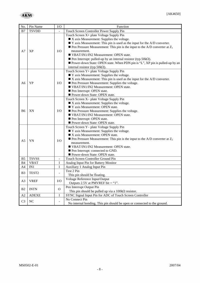
No. Pin Name I/O Function B7 TSVDD - Touch Screen Controller Power Supply Pin
A7 XP I/O
Touch Screen X+ plate Voltage Supply Pin X axis Measurement: Supplies the voltage. Y axis Measurement: This pin is used as the input for the A/D converter. Pen Pressure Measurement: This pin is the input to the A/D converter at Z1 measurement. VBAT/IN1/IN2 Measurement: OPEN state. Pen Interrupt: pulled-up by an internal resistor (typ.50kΩ). Power-down State: OPEN state. When PDN pin is “L”, XP pin is pulled-up by an
internal resistor (typ.50kΩ).
A6 YP I/O
Touch Screen Y+ plate Voltage Supply Pin Y axis Measurement: Supplies the voltage. X axis Measurement: This pin is used as the input for the A/D converter. Pen Pressure Measurement: Supplies the voltage. VBAT/IN1/IN2 Measurement: OPEN state. Pen Interrupt: OPEN state. Power-down State: OPEN state.
B6 XN I/O
Touch Screen X− plate Voltage Supply Pin X axis Measurement: Supplies the voltage. Y axis Measurement: OPEN state. Pen Pressure Measurement: Supplies the voltage. VBAT/IN1/IN2 Measurement: OPEN state. Pen Interrupt: OPEN state. Power-down State: OPEN state.
A5 YN I/O
Touch Screen Y− plate Voltage Supply Pin Y axis Measurement: Supplies the voltage. X axis Measurement: OPEN state. Pen Pressure Measurement: This pin is the input to the A/D converter at Z2 measurement. VBAT/IN1/IN2 Measurement: OPEN state. Pen Interrupt: connected to GND. Power-down State: OPEN state.
B5 TSVSS - Touch Screen Controller Ground Pin B4 VBAT I Analog Input Pin for Battery Monitor A4 IN1 I Auxiliary 1 Analog Input Pin
B3 TEST2 - Test 2 Pin This pin should be floating.
A3 VREF I/O Voltage Reference Input/Output Outputs 2.5V at PMVREF bit = “1”.
B2 INTN O Pen Interrupt Output Pin This pin should be pulled up via a 100kΩ resistor.
A2 ADEXE I SYNC Signal Input Pin for ADC of Touch Screen Controller
C3 NC - No Connect Pin No internal bonding. This pin should be open or connected to the ground.

[AK4650]
MS0502-E-01 2007/04 - 9 -
■ Handling of Unused Pin The unused I/O pins should be processed appropriately as below. Classification Pin Name Setting
Analog
MIN, MOUT2, MUTET, HDT, SPP, SPN, HPR, HPL, MOUT−, MOUT+, AIN, MICOUT, MDT/RIN, MPE/LIN, EXT/MIC+, INT/MIC−, MPI, AUXIN−, AUXIN+, BEEP/IN2, XP, YP, XN, YN, VBAT, IN1, INTN
These pins should be open.
Digital XTO This pin should be open.
[AK4650]
MS0502-E-01 2007/04 - 10 -
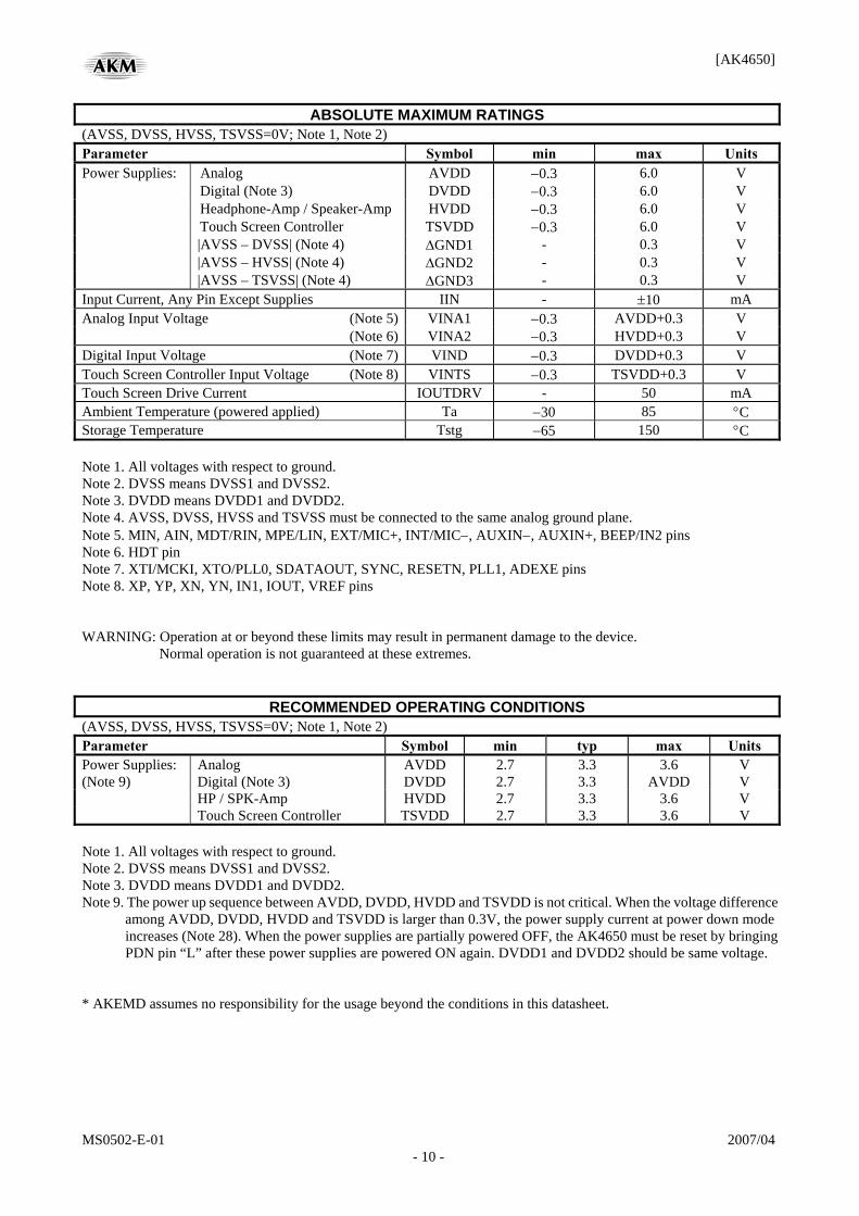
ABSOLUTE MAXIMUM RATINGS (AVSS, DVSS, HVSS, TSVSS=0V; Note 1, Note 2) Parameter Symbol min max Units Power Supplies: Analog AVDD −0.3 6.0 V Digital (Note 3) DVDD −0.3 6.0 V Headphone-Amp / Speaker-Amp HVDD −0.3 6.0 V Touch Screen Controller TSVDD −0.3 6.0 V |AVSS – DVSS| (Note 4) ΔGND1 - 0.3 V |AVSS – HVSS| (Note 4) ΔGND2 - 0.3 V |AVSS – TSVSS| (Note 4) ΔGND3 - 0.3 V Input Current, Any Pin Except Supplies IIN - ±10 mA Analog Input Voltage (Note 5) VINA1 −0.3 AVDD+0.3 V (Note 6) VINA2 −0.3 HVDD+0.3 V Digital Input Voltage (Note 7) VIND −0.3 DVDD+0.3 V Touch Screen Controller Input Voltage (Note 8) VINTS −0.3 TSVDD+0.3 V Touch Screen Drive Current IOUTDRV - 50 mA Ambient Temperature (powered applied) Ta −30 85 °C Storage Temperature Tstg −65 150 °C Note 1. All voltages with respect to ground. Note 2. DVSS means DVSS1 and DVSS2. Note 3. DVDD means DVDD1 and DVDD2. Note 4. AVSS, DVSS, HVSS and TSVSS must be connected to the same analog ground plane. Note 5. MIN, AIN, MDT/RIN, MPE/LIN, EXT/MIC+, INT/MIC−, AUXIN−, AUXIN+, BEEP/IN2 pins Note 6. HDT pin Note 7. XTI/MCKI, XTO/PLL0, SDATAOUT, SYNC, RESETN, PLL1, ADEXE pins Note 8. XP, YP, XN, YN, IN1, IOUT, VREF pins WARNING: Operation at or beyond these limits may result in permanent damage to the device.
Normal operation is not guaranteed at these extremes.
RECOMMENDED OPERATING CONDITIONS (AVSS, DVSS, HVSS, TSVSS=0V; Note 1, Note 2) Parameter Symbol min typ max Units Power Supplies: Analog AVDD 2.7 3.3 3.6 V (Note 9) Digital (Note 3) DVDD 2.7 3.3 AVDD V HP / SPK-Amp HVDD 2.7 3.3 3.6 V Touch Screen Controller TSVDD 2.7 3.3 3.6 V Note 1. All voltages with respect to ground. Note 2. DVSS means DVSS1 and DVSS2. Note 3. DVDD means DVDD1 and DVDD2. Note 9. The power up sequence between AVDD, DVDD, HVDD and TSVDD is not critical. When the voltage difference
among AVDD, DVDD, HVDD and TSVDD is larger than 0.3V, the power supply current at power down mode increases (Note 28). When the power supplies are partially powered OFF, the AK4650 must be reset by bringing PDN pin “L” after these power supplies are powered ON again. DVDD1 and DVDD2 should be same voltage.
* AKEMD assumes no responsibility for the usage beyond the conditions in this datasheet.
[AK4650]
MS0502-E-01 2007/04 - 11 -
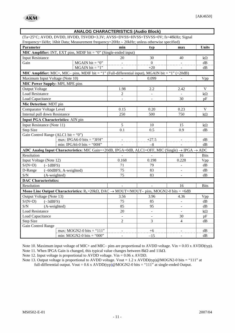
ANALOG CHARACTERISTICS (Audio Block) (Ta=25°C; AVDD, DVDD, HVDD, TSVDD=3.3V; AVSS=DVSS=HVSS=TSVSS=0V; fs=48kHz; Signal Frequency=1kHz; 16bit Data; Measurement frequency=20Hz ∼ 20kHz; unless otherwise specified) Parameter min typ max Units MIC Amplifier: INT, EXT pins, MDIF bit = “0” (Single-ended input) Input Resistance 20 30 40 kΩ Gain MGAIN bit = “0” - 0 - dB MGAIN bit = “1” - +20 - dB MIC Amplifier: MIC+, MIC− pins, MDIF bit = “1” (Full-differential input), MGAIN bit = “1” (+20dB) Maximum Input Voltage (Note 10) - 0.099 - Vpp MIC Power Supply: MPI, MPE pins Output Voltage 1.98 2.2 2.42 V Load Resistance 2 - - kΩ Load Capacitance - - 30 pF Mic Detection: MDT pin Comparator Voltage Level 0.15 0.20 0.23 V Internal pull down Resistance 250 500 750 kΩ Input PGA Characteristics: AIN pin Input Resistance (Note 11) 5 10 15 kΩ Step Size 0.1 0.5 0.9 dB Gain Control Range (ALC1 bit = “0”) max: IPGA6-0 bits = “3FH” - +27.5 - dB min: IPGA6-0 bits = “00H” - −8 - dB ADC Analog Input Characteristics: MIC Gain=+20dB, IPGA=0dB, ALC1=OFF, MIC (Single) → IPGA → ADC Resolution - - 16 Bits Input Voltage (Note 12) 0.168 0.198 0.228 Vpp S/(N+D) (−1dBFS) 71 79 - dB D-Range (−60dBFS, A-weighted) 75 83 - dB S/N (A-weighted) 75 83 - dB DAC Characteristics: Resolution - - 16 Bits Mono Line Output Characteristics: RL=20kΩ, DAC → MOUT+/MOUT− pins, MOGN2-0 bits = +6dB Output Voltage (Note 13) 3.56 3.96 4.36 Vpp S/(N+D) (−3dBFS) 75 85 - dB S/N (A-weighted) 85 95 - dB Load Resistance 20 - - kΩ Load Capacitance - - 30 pF Step Size 2 3 4 dB Gain Control Range max: MOGN2-0 bits = “111” - +6 - dB min: MOGN2-0 bits = “000” - −15 - dB Note 10. Maximum input voltage of MIC+ and MIC− pins are proportional to AVDD voltage. Vin = 0.03 x AVDD(typ). Note 11. When IPGA Gain is changed, this typical value changes between 8kΩ and 11kΩ. Note 12. Input voltage is proportional to AVDD voltage. Vin = 0.06 x AVDD. Note 13. Output voltage is proportional to AVDD voltage. Vout = 1.2 x AVDD(typ)@MOGN2-0 bits = “111” at
full-differential output. Vout = 0.6 x AVDD(typ)@MOGN2-0 bits = “111” at single-ended Output.
[AK4650]
MS0502-E-01 2007/04 - 12 -
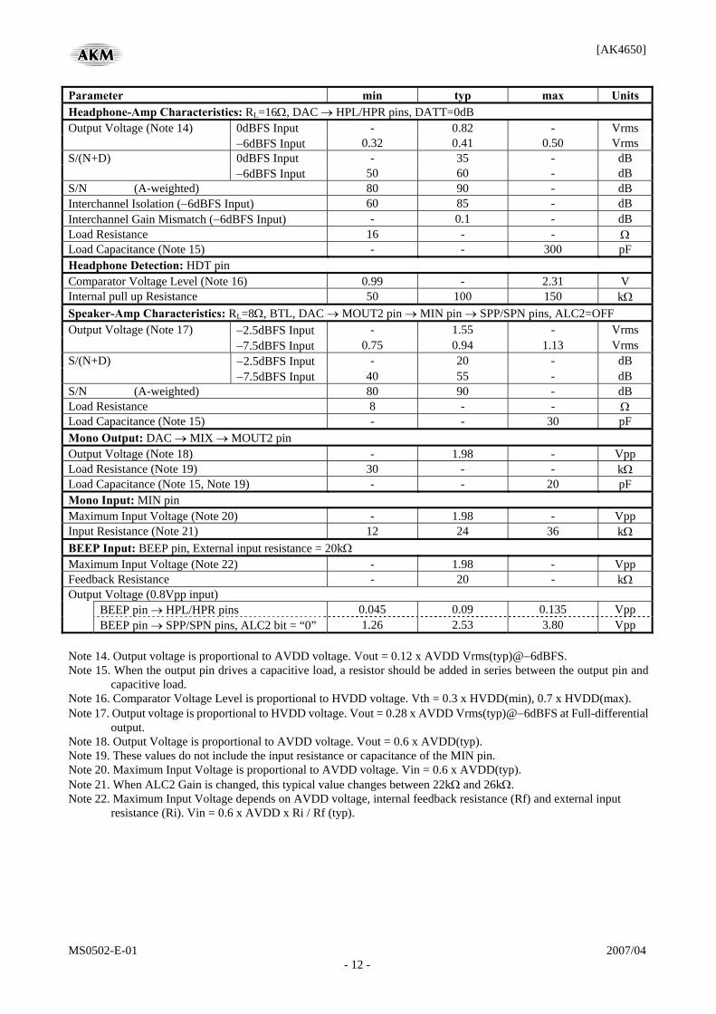
Parameter min typ max Units Headphone-Amp Characteristics: RL=16Ω, DAC → HPL/HPR pins, DATT=0dB Output Voltage (Note 14) 0dBFS Input - 0.82 - Vrms −6dBFS Input 0.32 0.41 0.50 Vrms S/(N+D) 0dBFS Input - 35 - dB −6dBFS Input 50 60 - dB S/N (A-weighted) 80 90 - dB Interchannel Isolation (−6dBFS Input) 60 85 - dB Interchannel Gain Mismatch (−6dBFS Input) - 0.1 - dB Load Resistance 16 - - Ω Load Capacitance (Note 15) - - 300 pF Headphone Detection: HDT pin Comparator Voltage Level (Note 16) 0.99 - 2.31 V Internal pull up Resistance 50 100 150 kΩ Speaker-Amp Characteristics: RL=8Ω, BTL, DAC → MOUT2 pin → MIN pin → SPP/SPN pins, ALC2=OFF Output Voltage (Note 17) −2.5dBFS Input - 1.55 - Vrms −7.5dBFS Input 0.75 0.94 1.13 Vrms S/(N+D) −2.5dBFS Input - 20 - dB −7.5dBFS Input 40 55 - dB S/N (A-weighted) 80 90 - dB Load Resistance 8 - - Ω Load Capacitance (Note 15) - - 30 pF Mono Output: DAC → MIX → MOUT2 pin Output Voltage (Note 18) - 1.98 - Vpp Load Resistance (Note 19) 30 - - kΩ Load Capacitance (Note 15, Note 19) - - 20 pF Mono Input: MIN pin Maximum Input Voltage (Note 20) - 1.98 - Vpp Input Resistance (Note 21) 12 24 36 kΩ BEEP Input: BEEP pin, External input resistance = 20kΩ Maximum Input Voltage (Note 22) - 1.98 - Vpp Feedback Resistance - 20 - kΩ Output Voltage (0.8Vpp input) BEEP pin → HPL/HPR pins 0.045 0.09 0.135 Vpp BEEP pin → SPP/SPN pins, ALC2 bit = “0” 1.26 2.53 3.80 Vpp Note 14. Output voltage is proportional to AVDD voltage. Vout = 0.12 x AVDD Vrms(typ)@−6dBFS. Note 15. When the output pin drives a capacitive load, a resistor should be added in series between the output pin and
capacitive load. Note 16. Comparator Voltage Level is proportional to HVDD voltage. Vth = 0.3 x HVDD(min), 0.7 x HVDD(max). Note 17. Output voltage is proportional to HVDD voltage. Vout = 0.28 x AVDD Vrms(typ)@−6dBFS at Full-differential
output. Note 18. Output Voltage is proportional to AVDD voltage. Vout = 0.6 x AVDD(typ). Note 19. These values do not include the input resistance or capacitance of the MIN pin. Note 20. Maximum Input Voltage is proportional to AVDD voltage. Vin = 0.6 x AVDD(typ). Note 21. When ALC2 Gain is changed, this typical value changes between 22kΩ and 26kΩ. Note 22. Maximum Input Voltage depends on AVDD voltage, internal feedback resistance (Rf) and external input
resistance (Ri). Vin = 0.6 x AVDD x Ri / Rf (typ).
[AK4650]
MS0502-E-01 2007/04 - 13 -
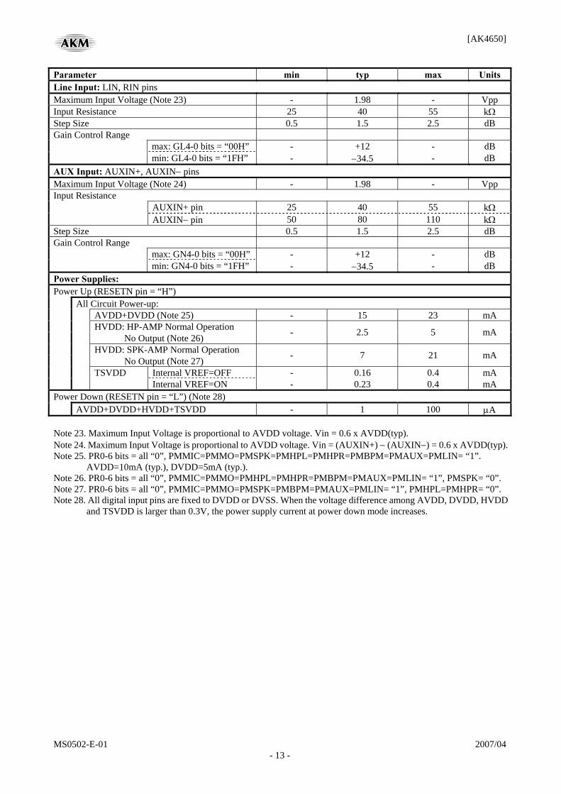
Parameter min typ max Units Line Input: LIN, RIN pins Maximum Input Voltage (Note 23) - 1.98 - Vpp Input Resistance 25 40 55 kΩ Step Size 0.5 1.5 2.5 dB Gain Control Range max: GL4-0 bits = “00H” - +12 - dB min: GL4-0 bits = “1FH” - −34.5 - dB AUX Input: AUXIN+, AUXIN− pins Maximum Input Voltage (Note 24) - 1.98 - Vpp Input Resistance AUXIN+ pin 25 40 55 kΩ AUXIN− pin 50 80 110 kΩ Step Size 0.5 1.5 2.5 dB Gain Control Range max: GN4-0 bits = “00H” - +12 - dB min: GN4-0 bits = “1FH” - −34.5 - dB Power Supplies: Power Up (RESETN pin = “H”) All Circuit Power-up: AVDD+DVDD (Note 25) - 15 23 mA
HVDD: HP-AMP Normal Operation No Output (Note 26) - 2.5 5 mA
HVDD: SPK-AMP Normal Operation No Output (Note 27) - 7 21 mA
TSVDD Internal VREF=OFF - 0.16 0.4 mA Internal VREF=ON - 0.23 0.4 mA Power Down (RESETN pin = “L”) (Note 28) AVDD+DVDD+HVDD+TSVDD - 1 100 μA Note 23. Maximum Input Voltage is proportional to AVDD voltage. Vin = 0.6 x AVDD(typ). Note 24. Maximum Input Voltage is proportional to AVDD voltage. Vin = (AUXIN+) − (AUXIN−) = 0.6 x AVDD(typ). Note 25. PR0-6 bits = all “0”, PMMIC=PMMO=PMSPK=PMHPL=PMHPR=PMBPM=PMAUX=PMLIN= “1”.
AVDD=10mA (typ.), DVDD=5mA (typ.). Note 26. PR0-6 bits = all “0”, PMMIC=PMMO=PMHPL=PMHPR=PMBPM=PMAUX=PMLIN= “1”, PMSPK= “0”. Note 27. PR0-6 bits = all “0”, PMMIC=PMMO=PMSPK=PMBPM=PMAUX=PMLIN= “1”, PMHPL=PMHPR= “0”. Note 28. All digital input pins are fixed to DVDD or DVSS. When the voltage difference among AVDD, DVDD, HVDD
and TSVDD is larger than 0.3V, the power supply current at power down mode increases.
[AK4650]
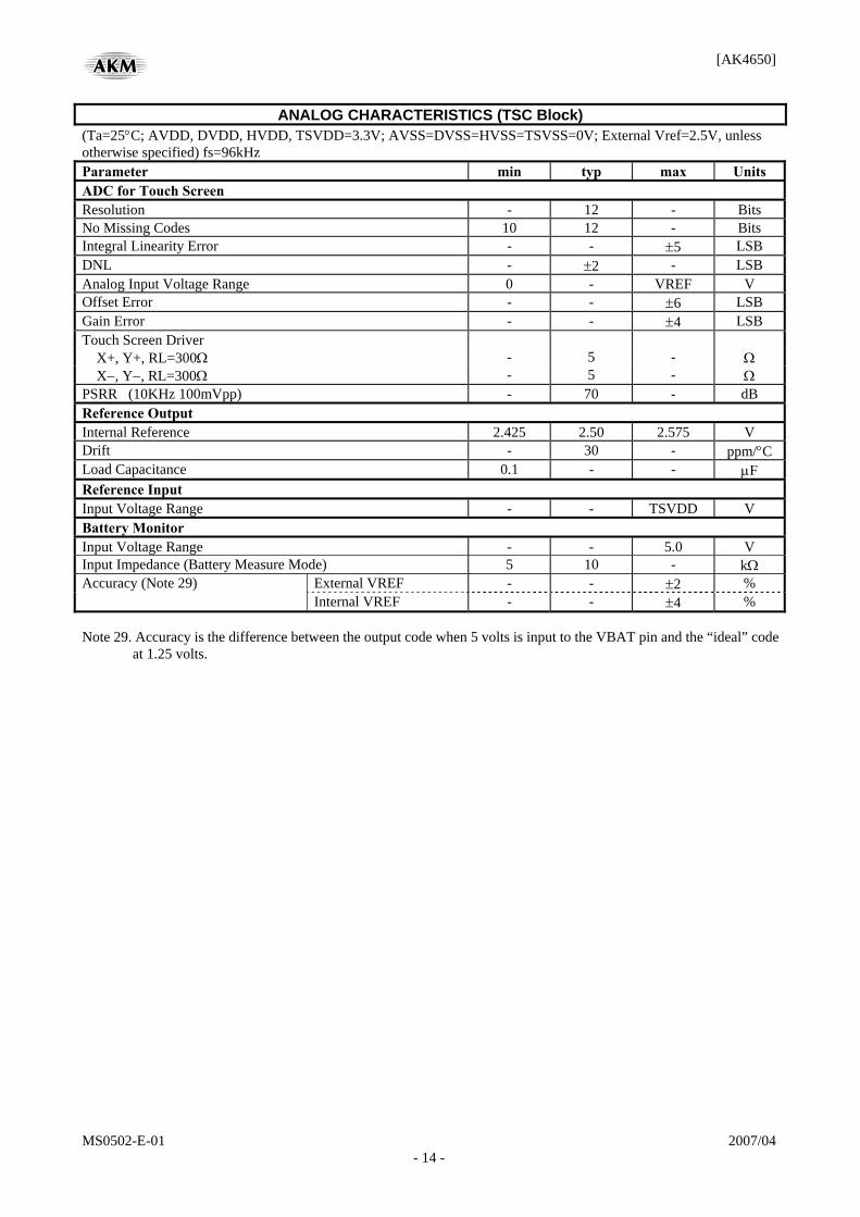
MS0502-E-01 2007/04 - 14 -
ANALOG CHARACTERISTICS (TSC Block) (Ta=25°C; AVDD, DVDD, HVDD, TSVDD=3.3V; AVSS=DVSS=HVSS=TSVSS=0V; External Vref=2.5V, unless otherwise specified) fs=96kHz Parameter min typ max Units ADC for Touch Screen Resolution - 12 - Bits No Missing Codes 10 12 - Bits Integral Linearity Error - - ±5 LSB DNL - ±2 - LSB Analog Input Voltage Range 0 - VREF V Offset Error - - ±6 LSB Gain Error - - ±4 LSB Touch Screen Driver
X+, Y+, RL=300Ω - 5 - Ω X−, Y−, RL=300Ω - 5 - Ω
PSRR (10KHz 100mVpp) - 70 - dB Reference Output Internal Reference 2.425 2.50 2.575 V Drift - 30 - ppm/°CLoad Capacitance 0.1 - - μF Reference Input Input Voltage Range - - TSVDD V Battery Monitor Input Voltage Range - - 5.0 V Input Impedance (Battery Measure Mode) 5 10 - kΩ Accuracy (Note 29) External VREF - - ±2 % Internal VREF - - ±4 % Note 29. Accuracy is the difference between the output code when 5 volts is input to the VBAT pin and the “ideal” code
at 1.25 volts.
[AK4650]
MS0502-E-01 2007/04 - 15 -
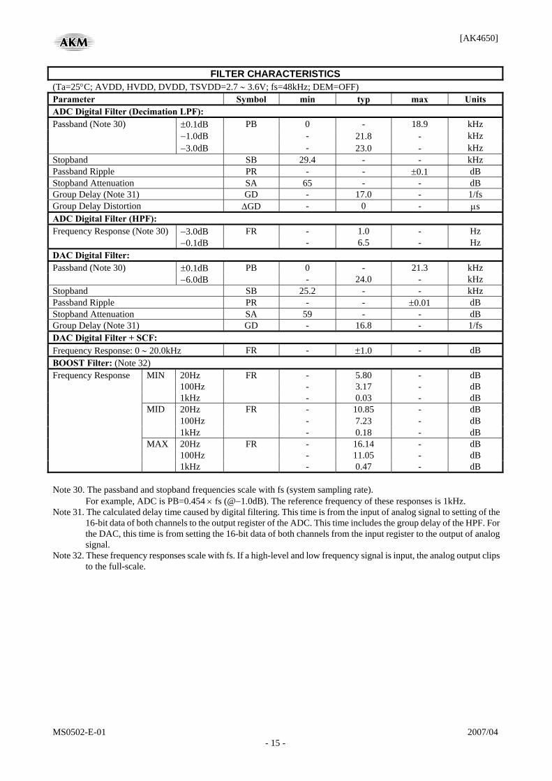
FILTER CHARACTERISTICS (Ta=25°C; AVDD, HVDD, DVDD, TSVDD=2.7 ∼ 3.6V; fs=48kHz; DEM=OFF) Parameter Symbol min typ max Units ADC Digital Filter (Decimation LPF): Passband (Note 30) ±0.1dB PB 0 - 18.9 kHz −1.0dB - 21.8 - kHz −3.0dB - 23.0 - kHz Stopband SB 29.4 - - kHz Passband Ripple PR - - ±0.1 dB Stopband Attenuation SA 65 - - dB Group Delay (Note 31) GD - 17.0 - 1/fs Group Delay Distortion ΔGD - 0 - μs ADC Digital Filter (HPF): Frequency Response (Note 30) −3.0dB FR - 1.0 - Hz −0.1dB - 6.5 - Hz DAC Digital Filter: Passband (Note 30) ±0.1dB PB 0 - 21.3 kHz −6.0dB - 24.0 - kHz Stopband SB 25.2 - - kHz Passband Ripple PR - - ±0.01 dB Stopband Attenuation SA 59 - - dB Group Delay (Note 31) GD - 16.8 - 1/fs DAC Digital Filter + SCF: Frequency Response: 0 ∼ 20.0kHz FR - ±1.0 - dB BOOST Filter: (Note 32)
MIN 20Hz FR - 5.80 - dB 100Hz - 3.17 - dB 1kHz - 0.03 - dB MID 20Hz FR - 10.85 - dB 100Hz - 7.23 - dB 1kHz - 0.18 - dB MAX 20Hz FR - 16.14 - dB 100Hz - 11.05 - dB
Frequency Response
1kHz - 0.47 - dB Note 30. The passband and stopband frequencies scale with fs (system sampling rate).
For example, ADC is PB=0.454 × fs (@−1.0dB). The reference frequency of these responses is 1kHz. Note 31. The calculated delay time caused by digital filtering. This time is from the input of analog signal to setting of the
16-bit data of both channels to the output register of the ADC. This time includes the group delay of the HPF. For the DAC, this time is from setting the 16-bit data of both channels from the input register to the output of analog signal.
Note 32. These frequency responses scale with fs. If a high-level and low frequency signal is input, the analog output clips to the full-scale.
[AK4650]
MS0502-E-01 2007/04 - 16 -
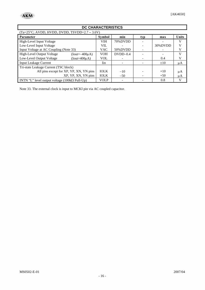
DC CHARACTERISTICS (Ta=25°C; AVDD, HVDD, DVDD, TSVDD=2.7 ∼ 3.6V) Parameter Symbol min typ max UnitsHigh-Level Input Voltage VIH 70%DVDD - - V Low-Level Input Voltage VIL - - 30%DVDD V Input Voltage at AC Coupling (Note 33) VAC 50%DVDD - - V High-Level Output Voltage (Iout=−400μA) VOH DVDD−0.4 - - V Low-Level Output Voltage (Iout=400μA) VOL - - 0.4 V Input Leakage Current Iin - - ±10 μA Tri-state Leakage Current (TSC block)
All pins except for XP, YP, XN, YN pins IOLK −10 - +10 μA XP, YP, XN, YN pins IOLK −50 - +50 μA
INTN “L” level output voltage (100kΩ Pull-Up) VOLP - - 0.8 V Note 33. The external clock is input to MCKI pin via AC coupled capacitor.
[AK4650]
MS0502-E-01 2007/04 - 17 -
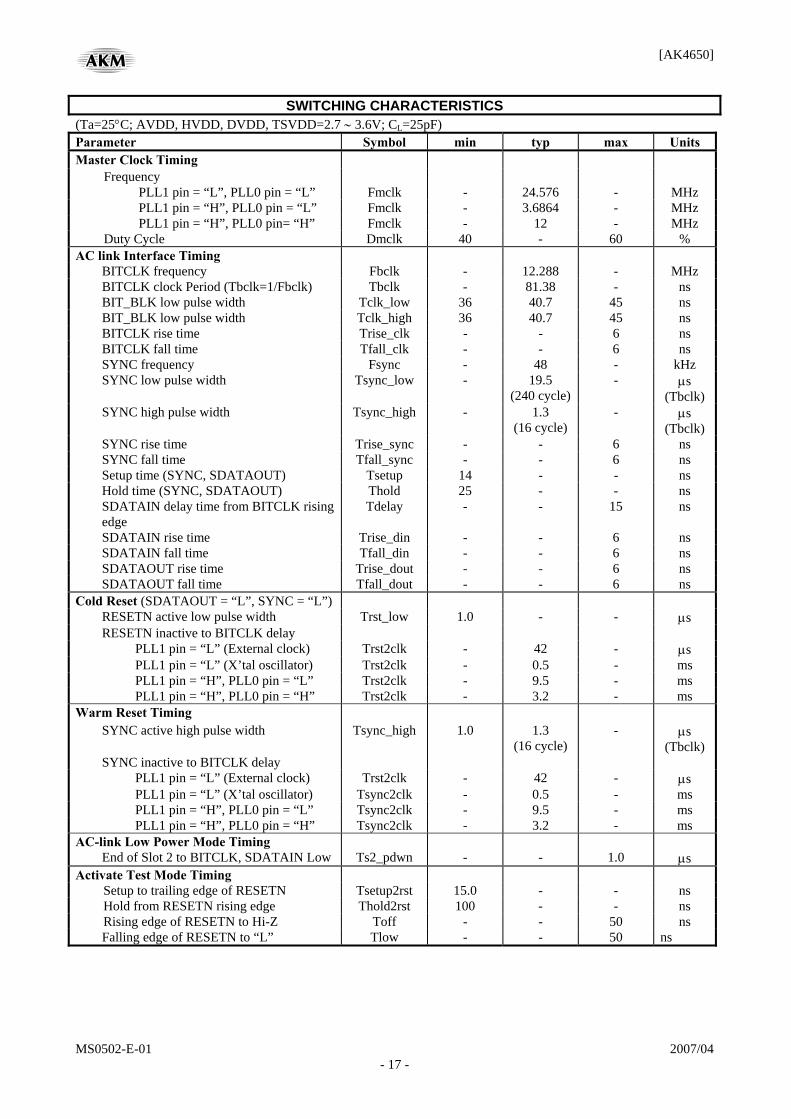
SWITCHING CHARACTERISTICS (Ta=25°C; AVDD, HVDD, DVDD, TSVDD=2.7 ∼ 3.6V; CL=25pF) Parameter Symbol min typ max Units Master Clock Timing
Frequency PLL1 pin = “L”, PLL0 pin = “L” Fmclk - 24.576 - MHz PLL1 pin = “H”, PLL0 pin = “L” Fmclk - 3.6864 - MHz PLL1 pin = “H”, PLL0 pin= “H” Fmclk - 12 - MHz
Duty Cycle Dmclk 40 - 60 % AC link Interface Timing
BITCLK frequency Fbclk - 12.288 - MHz BITCLK clock Period (Tbclk=1/Fbclk) Tbclk - 81.38 - ns BIT_BLK low pulse width Tclk_low 36 40.7 45 ns BIT_BLK low pulse width Tclk_high 36 40.7 45 ns BITCLK rise time Trise_clk - - 6 ns BITCLK fall time Tfall_clk - - 6 ns SYNC frequency Fsync - 48 - kHz SYNC low pulse width Tsync_low - 19.5
(240 cycle) - μs
(Tbclk)SYNC high pulse width Tsync_high - 1.3
(16 cycle) - μs
(Tbclk)SYNC rise time Trise_sync - - 6 ns SYNC fall time Tfall_sync - - 6 ns Setup time (SYNC, SDATAOUT) Tsetup 14 - - ns Hold time (SYNC, SDATAOUT) Thold 25 - - ns SDATAIN delay time from BITCLK rising edge
Tdelay - - 15 ns
SDATAIN rise time Trise_din - - 6 ns SDATAIN fall time Tfall_din - - 6 ns SDATAOUT rise time Trise_dout - - 6 ns SDATAOUT fall time Tfall_dout - - 6 ns
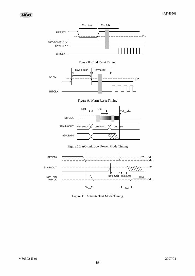
Cold Reset (SDATAOUT = “L”, SYNC = “L”) RESETN active low pulse width Trst_low 1.0 - - μs RESETN inactive to BITCLK delay
PLL1 pin = “L” (External clock) Trst2clk - 42 - μs PLL1 pin = “L” (X’tal oscillator) Trst2clk - 0.5 - ms PLL1 pin = “H”, PLL0 pin = “L” Trst2clk - 9.5 - ms PLL1 pin = “H”, PLL0 pin = “H” Trst2clk - 3.2 - ms Warm Reset Timing
SYNC active high pulse width Tsync_high 1.0 1.3 (16 cycle)
- μs (Tbclk)
SYNC inactive to BITCLK delay PLL1 pin = “L” (External clock) Trst2clk - 42 - μs PLL1 pin = “L” (X’tal oscillator) Tsync2clk - 0.5 - ms PLL1 pin = “H”, PLL0 pin = “L” Tsync2clk - 9.5 - ms PLL1 pin = “H”, PLL0 pin = “H” Tsync2clk - 3.2 - ms AC-link Low Power Mode Timing
End of Slot 2 to BITCLK, SDATAIN Low Ts2_pdwn - - 1.0 μs Activate Test Mode Timing
Setup to trailing edge of RESETN Tsetup2rst 15.0 - - ns Hold from RESETN rising edge Thold2rst 100 - - ns Rising edge of RESETN to Hi-Z Toff - - 50 ns Falling edge of RESETN to “L” Tlow - - 50 ns
[AK4650]
MS0502-E-01 2007/04 - 18 -
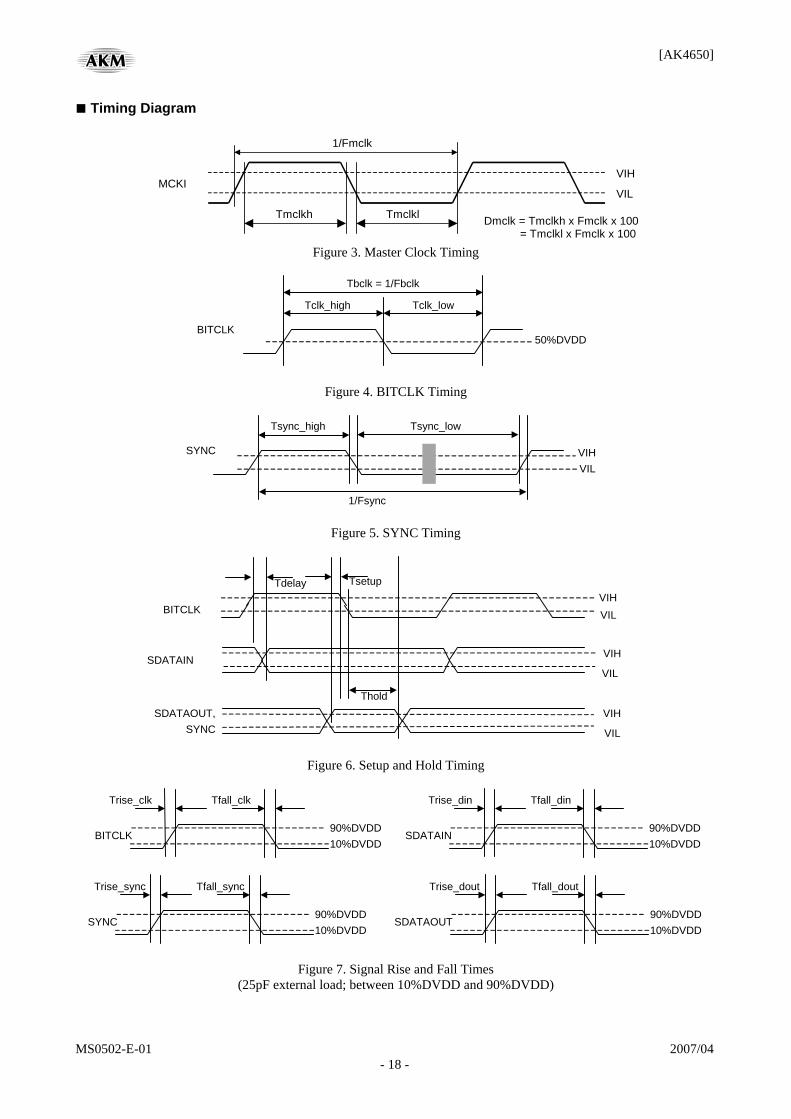
■ Timing Diagram
1/Fmclk
MCKI VIH
VIL
TmclklTmclkh Dmclk = Tmclkh x Fmclk x 100 = Tmclkl x Fmclk x 100
Figure 3. Master Clock Timing
Tclk_low
50%DVDD
Tclk_high
BITCLK
Tbclk = 1/Fbclk
Figure 4. BITCLK Timing
Tsync_low
VIH VIL
1/Fsync
Tsync_high
SYNC
Figure 5. SYNC Timing
SDATAIN
SDATAOUT, SYNC
VIH
Thold
Tsetup
VIL BITCLK
VIH
VIL
Tdelay
VIH
VIL
Figure 6. Setup and Hold Timing
Trise_clk
BITCLK
Tfall_clk
90%DVDD
10%DVDD
Trise_din
SDATAIN
Tfall_din
90%DVDD
10%DVDD
Trise_sync
SYNC
Tfall_sync
90%DVDD
10%DVDD
Trise_dout
SDATAOUT
Tfall_dout
90%DVDD
10%DVDD
Figure 7. Signal Rise and Fall Times
(25pF external load; between 10%DVDD and 90%DVDD)
[AK4650]
MS0502-E-01 2007/04 - 19 -
BITCLK
VIL RESET#
Trst2clkTrst_low
SYNC= “L”SDATAOUT= “L”
Figure 8. Cold Reset Timing
VIH
Tsync2clk Tsync_high
BITCLK
SYNC
Figure 9. Warm Reset Timing
Slot
Write to 0x26
BITCLK
SDATAIN
SDATAOUT
Ts2_pdwnSlot
Data PR4=1 Don’t care
Figure 10. AC-link Low Power Mode Timing
VIH
VIH
Tsetup2rst
Toff
SDATAIN BITCLK
SDATAOUT
HI-Z
RESET#
VIL
Tlow
VIL
Thold2rst
Figure 11. Activate Test Mode Timing
[AK4650]
MS0502-E-01 2007/04 - 20 -
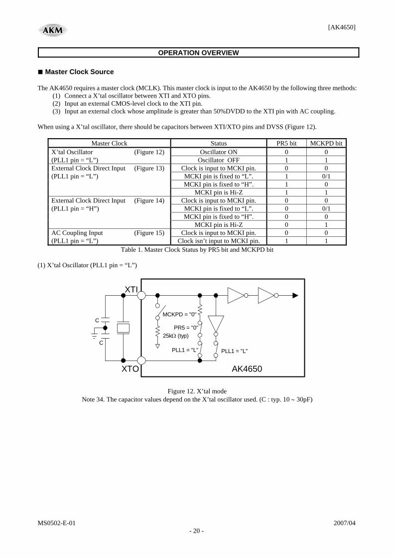
OPERATION OVERVIEW ■ Master Clock Source The AK4650 requires a master clock (MCLK). This master clock is input to the AK4650 by the following three methods:
(1) Connect a X’tal oscillator between XTI and XTO pins. (2) Input an external CMOS-level clock to the XTI pin. (3) Input an external clock whose amplitude is greater than 50%DVDD to the XTI pin with AC coupling.
When using a X’tal oscillator, there should be capacitors between XTI/XTO pins and DVSS (Figure 12).
Master Clock Status PR5 bit MCKPD bitX’tal Oscillator (Figure 12) Oscillator ON 0 0 (PLL1 pin = “L”) Oscillator OFF 1 1 External Clock Direct Input (Figure 13) Clock is input to MCKI pin. 0 0 (PLL1 pin = “L”) MCKI pin is fixed to “L”. 1 0/1 MCKI pin is fixed to “H”. 1 0 MCKI pin is Hi-Z 1 1 External Clock Direct Input (Figure 14) Clock is input to MCKI pin. 0 0 (PLL1 pin = “H”) MCKI pin is fixed to “L”. 0 0/1 MCKI pin is fixed to “H”. 0 0 MCKI pin is Hi-Z 0 1 AC Coupling Input (Figure 15) Clock is input to MCKI pin. 0 0 (PLL1 pin = “L”) Clock isn’t input to MCKI pin. 1 1
Table 1. Master Clock Status by PR5 bit and MCKPD bit (1) X’tal Oscillator (PLL1 pin = “L”)
XTI
XTO AK4650
25kΩ (typ)
MCKPD = "0"
PR5 = "0"C
CPLL1 = "L" PLL1 = "L"
Figure 12. X’tal mode Note 34. The capacitor values depend on the X’tal oscillator used. (C : typ. 10 ∼ 30pF)
[AK4650]
MS0502-E-01 2007/04 - 21 -
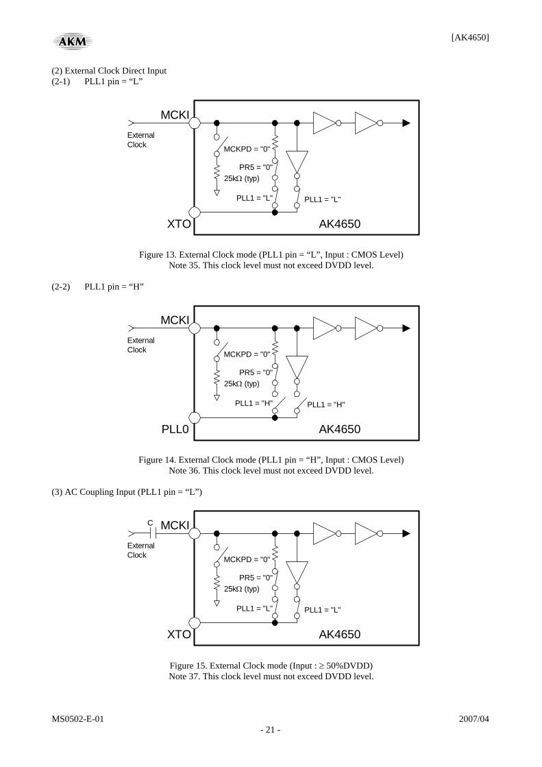
(2) External Clock Direct Input (2-1) PLL1 pin = “L”
MCKI
XTO AK4650
25kΩ (typ)
MCKPD = "0"
PR5 = "0"
PLL1 = "L" PLL1 = "L"
ExternalClock
Figure 13. External Clock mode (PLL1 pin = “L”, Input : CMOS Level) Note 35. This clock level must not exceed DVDD level.
(2-2) PLL1 pin = “H”
MCKI
PLL0 AK4650
25kΩ (typ)
MCKPD = "0"
PR5 = "0"
PLL1 = "H" PLL1 = "H"
ExternalClock
Figure 14. External Clock mode (PLL1 pin = “H”, Input : CMOS Level) Note 36. This clock level must not exceed DVDD level.
(3) AC Coupling Input (PLL1 pin = “L”)
MCKI
XTO AK4650
25kΩ (typ)
MCKPD = "0"
PR5 = "0"
PLL1 = "L" PLL1 = "L"
ExternalClock
C
Figure 15. External Clock mode (Input : ≥ 50%DVDD) Note 37. This clock level must not exceed DVDD level.
[AK4650]
MS0502-E-01 2007/04 - 22 -
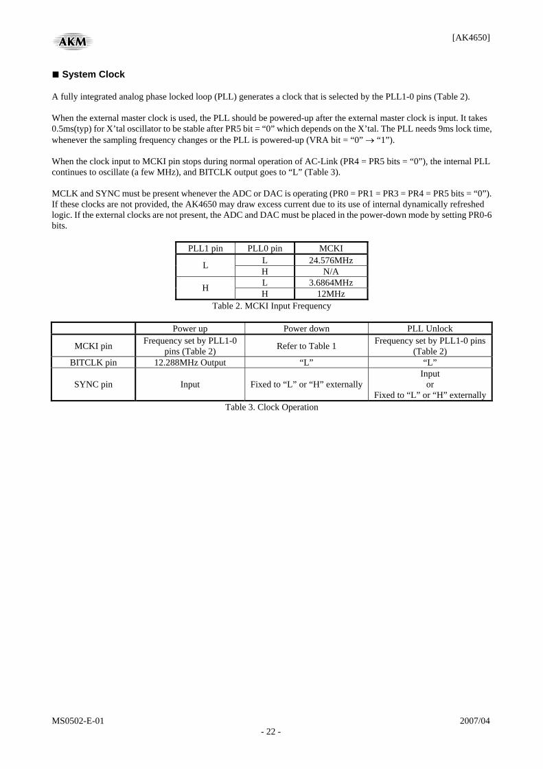
■ System Clock A fully integrated analog phase locked loop (PLL) generates a clock that is selected by the PLL1-0 pins (Table 2). When the external master clock is used, the PLL should be powered-up after the external master clock is input. It takes 0.5ms(typ) for X’tal oscillator to be stable after PR5 bit = “0” which depends on the X’tal. The PLL needs 9ms lock time, whenever the sampling frequency changes or the PLL is powered-up (VRA bit = “0” → “1”). When the clock input to MCKI pin stops during normal operation of AC-Link (PR4 = PR5 bits = “0”), the internal PLL continues to oscillate (a few MHz), and BITCLK output goes to “L” (Table 3). MCLK and SYNC must be present whenever the ADC or DAC is operating (PR0 = PR1 = PR3 = PR4 = PR5 bits = “0”). If these clocks are not provided, the AK4650 may draw excess current due to its use of internal dynamically refreshed logic. If the external clocks are not present, the ADC and DAC must be placed in the power-down mode by setting PR0-6 bits.
PLL1 pin PLL0 pin MCKI L 24.576MHz L H N/A L 3.6864MHz H H 12MHz
Table 2. MCKI Input Frequency
Power up Power down PLL Unlock
MCKI pin Frequency set by PLL1-0 pins (Table 2) Refer to Table 1 Frequency set by PLL1-0 pins
(Table 2) BITCLK pin 12.288MHz Output “L” “L”
SYNC pin Input Fixed to “L” or “H” externallyInput
or Fixed to “L” or “H” externally
Table 3. Clock Operation
[AK4650]
MS0502-E-01 2007/04 - 23 -
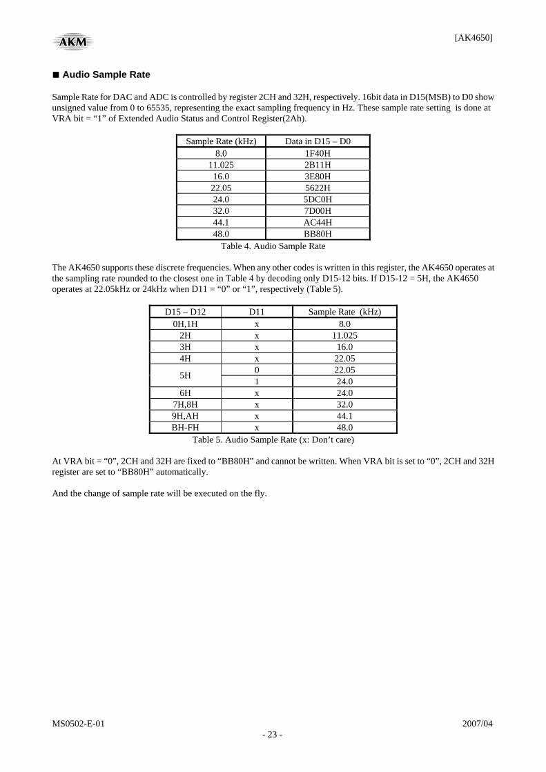
■ Audio Sample Rate Sample Rate for DAC and ADC is controlled by register 2CH and 32H, respectively. 16bit data in D15(MSB) to D0 show unsigned value from 0 to 65535, representing the exact sampling frequency in Hz. These sample rate setting is done at VRA bit = “1” of Extended Audio Status and Control Register(2Ah).
Sample Rate (kHz) Data in D15 – D0 8.0 1F40H
11.025 2B11H 16.0 3E80H
22.05 5622H 24.0 5DC0H 32.0 7D00H 44.1 AC44H 48.0 BB80H
Table 4. Audio Sample Rate The AK4650 supports these discrete frequencies. When any other codes is written in this register, the AK4650 operates at the sampling rate rounded to the closest one in Table 4 by decoding only D15-12 bits. If D15-12 = 5H, the AK4650 operates at 22.05kHz or 24kHz when D11 = “0” or “1”, respectively (Table 5).
D15 – D12 D11 Sample Rate (kHz) 0H,1H x 8.0
2H x 11.025 3H x 16.0 4H x 22.05
0 22.05 5H 1 24.0
6H x 24.0 7H,8H x 32.0 9H,AH x 44.1 BH-FH x 48.0
Table 5. Audio Sample Rate (x: Don’t care) At VRA bit = “0”, 2CH and 32H are fixed to “BB80H” and cannot be written. When VRA bit is set to “0”, 2CH and 32H register are set to “BB80H” automatically. And the change of sample rate will be executed on the fly.
[AK4650]
MS0502-E-01 2007/04 - 24 -
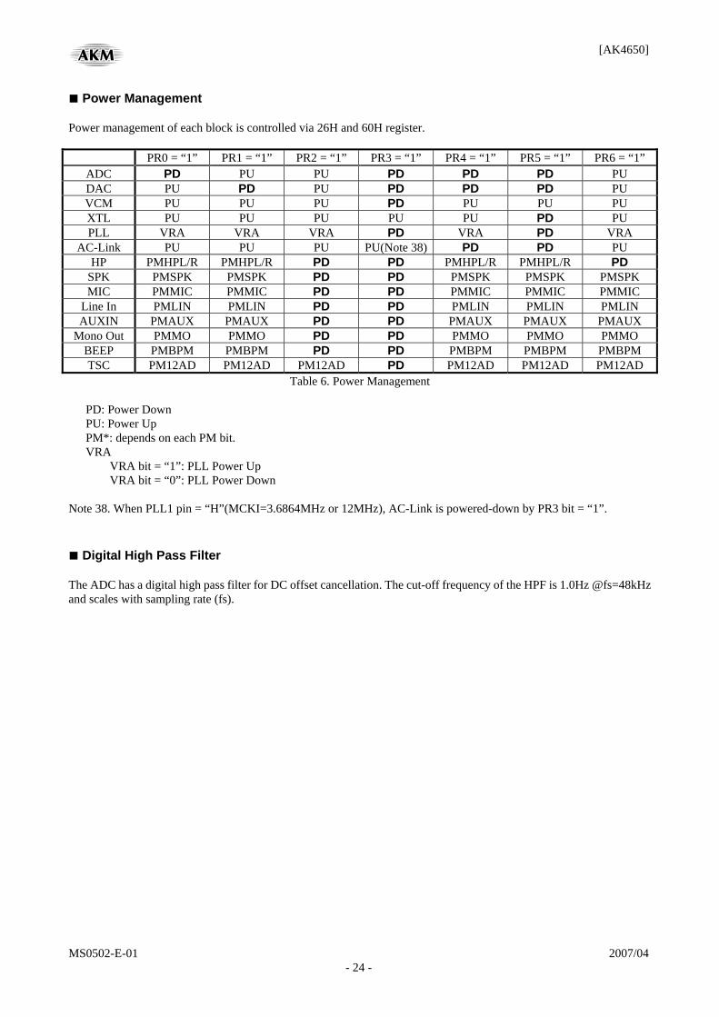
■ Power Management Power management of each block is controlled via 26H and 60H register.
PR0 = “1” PR1 = “1” PR2 = “1” PR3 = “1” PR4 = “1” PR5 = “1” PR6 = “1” ADC PD PU PU PD PD PD PU DAC PU PD PU PD PD PD PU VCM PU PU PU PD PU PU PU XTL PU PU PU PU PU PD PU PLL VRA VRA VRA PD VRA PD VRA
AC-Link PU PU PU PU(Note 38) PD PD PU HP PMHPL/R PMHPL/R PD PD PMHPL/R PMHPL/R PD
SPK PMSPK PMSPK PD PD PMSPK PMSPK PMSPK MIC PMMIC PMMIC PD PD PMMIC PMMIC PMMIC
Line In PMLIN PMLIN PD PD PMLIN PMLIN PMLIN AUXIN PMAUX PMAUX PD PD PMAUX PMAUX PMAUX
Mono Out PMMO PMMO PD PD PMMO PMMO PMMO BEEP PMBPM PMBPM PD PD PMBPM PMBPM PMBPM TSC PM12AD PM12AD PM12AD PD PM12AD PM12AD PM12AD
Table 6. Power Management
PD: Power Down PU: Power Up PM*: depends on each PM bit. VRA
VRA bit = “1”: PLL Power Up VRA bit = “0”: PLL Power Down
Note 38. When PLL1 pin = “H”(MCKI=3.6864MHz or 12MHz), AC-Link is powered-down by PR3 bit = “1”. ■ Digital High Pass Filter The ADC has a digital high pass filter for DC offset cancellation. The cut-off frequency of the HPF is 1.0Hz @fs=48kHz and scales with sampling rate (fs).
[AK4650]
MS0502-E-01 2007/04 - 25 -
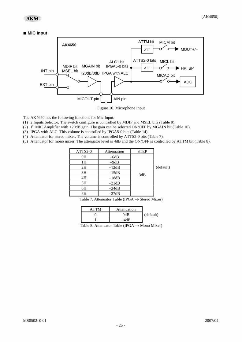
■ MIC Input
ADC
+20dB/0dB IPGA with ALCHP, SP
MOUT+/− ATT
MICAD bit
MICM bit
MICL bit ATT
ATTM bit
ATTS2-0 bitsMGAIN bit IPGA5-0 bits
ALC1 bit
INT pin
EXT pin
MSEL bit MDIF bit
AK4650
MICOUT pin AIN pin
Figure 16. Microphone Input The AK4650 has the following functions for Mic Input. (1) 2 Inputs Selector. The switch configure is controlled by MDIF and MSEL bits (Table 9). (2) 1st MIC Amplifier with +20dB gain, The gain can be selected ON/OFF by MGAIN bit (Table 10). (3) IPGA with ALC. This volume is controlled by IPGA5-0 bits (Table 14). (4) Attenuator for stereo mixer. The volume is controlled by ATTS2-0 bits (Table 7). (5) Attenuator for mono mixer. The attenuator level is 4dB and the ON/OFF is controlled by ATTM bit (Table 8).
ATTS2-0 Attenuation STEP 0H −6dB 1H −9dB 2H −12dB (default)3H −15dB 4H −18dB 5H −21dB 6H −24dB 7H −27dB
3dB
Table 7. Attenuator Table (IPGA → Stereo Mixer)
ATTM Attenuation
0 0dB (default)1 −4dB
Table 8. Attenuator Table (IPGA → Mono Mixer)
[AK4650]
MS0502-E-01 2007/04 - 26 -
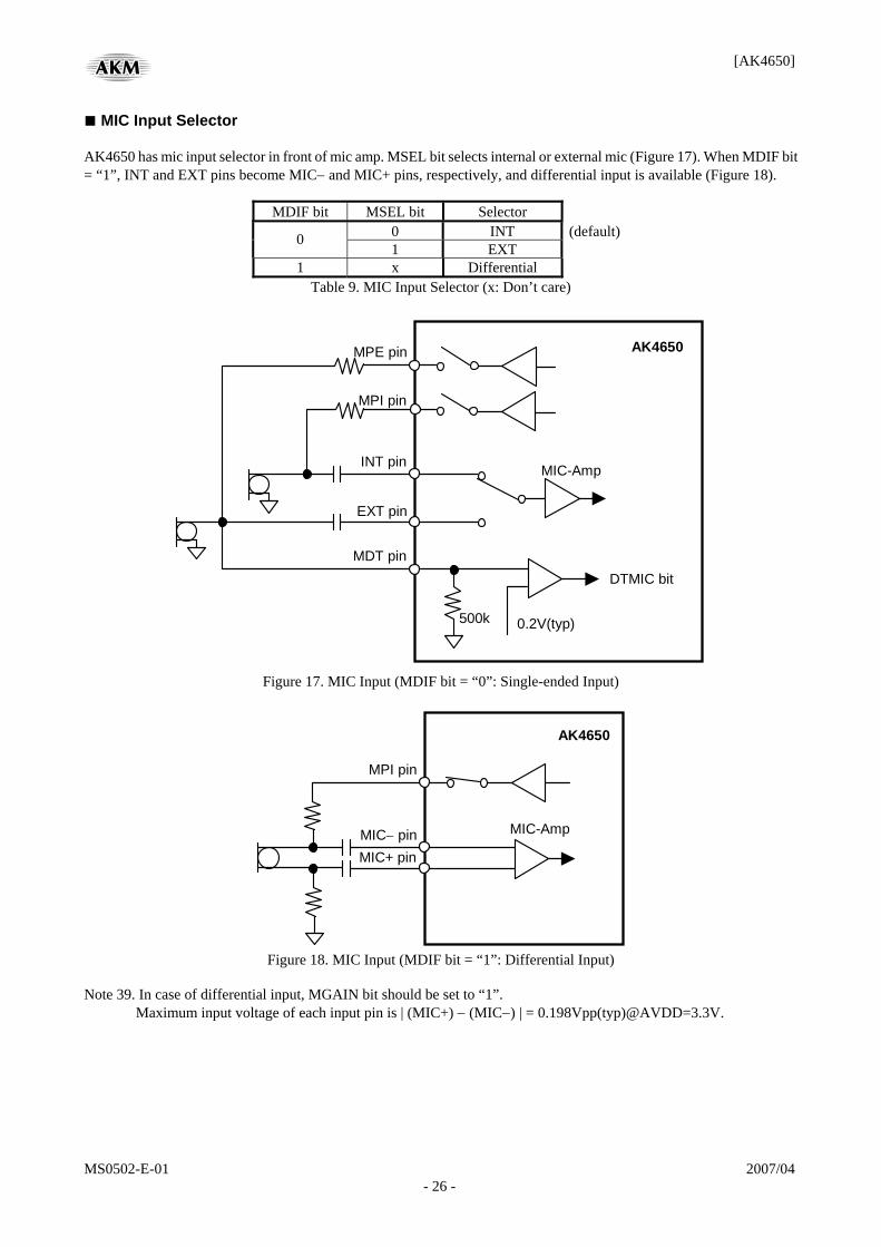
■ MIC Input Selector AK4650 has mic input selector in front of mic amp. MSEL bit selects internal or external mic (Figure 17). When MDIF bit = “1”, INT and EXT pins become MIC− and MIC+ pins, respectively, and differential input is available (Figure 18).
MDIF bit MSEL bit Selector 0 INT (default)0 1 EXT
1 x Differential Table 9. MIC Input Selector (x: Don’t care)
INT pin
EXT pin
MPI pin
MPE pin
DTMIC bit MDT pin
0.2V(typ) 500k
AK4650
MIC-Amp
Figure 17. MIC Input (MDIF bit = “0”: Single-ended Input)
MIC− pinMIC+ pin
MPI pin
AK4650
MIC-Amp
Figure 18. MIC Input (MDIF bit = “1”: Differential Input)
Note 39. In case of differential input, MGAIN bit should be set to “1”.
Maximum input voltage of each input pin is | (MIC+) − (MIC−) | = 0.198Vpp(typ)@AVDD=3.3V.
[AK4650]
MS0502-E-01 2007/04 - 27 -
■ MIC Gain Amplifier The AK4650 has a Gain Amplifier for Microphone input. The gain is 0dB or +20dB, selected by the MGAIN bit. The typical input impedance is 30kΩ.
MGAIN bit Input Gain 0 0dB (default)1 +20dB
Table 10. MIC Input Gain ■ MIC Power The MPI and MPE pins supply power for the Microphone. These output voltages are 2.2V (typ) and load resistance is 2kΩ (min). MPWRI and MPWRE bits control output from MPI and MPE pins, respectively. When LNMP bit = “1”, MPE pin becomes LIN pin.
PMMIC bit MPWRI bit MPI pin 0 x Hi-Z (default)
0 Hi-Z 1 1 Output Table 11. Internal Microphone Power Supply (x: Don’t care)
PMMIC bit MPWRE bit MPE pin
0 x Hi-Z (default)0 Hi-Z 1 1 Output
Table 12. External Microphone Power Supply (x: Don’t care) ■ MIC Detection Function The AK4650 includes the detection function of microphone. Example of the detection of external microphone.
(1) MPWRE bit = “1”. (2) MPE drives external microphone. (3) DTMIC bit is set by Table 13.
Input Level of MDT DTMIC bit External microphone
> 0.247V 1 Connect < 0.165V 0 Disconnect
Table 13. Microphone detection result When RNMD bit = “1”, MDT pin becomes RIN pin.
[AK4650]
MS0502-E-01 2007/04 - 28 -
■ Manual Mode The AK4650 becomes a manual mode at ALC1 bit = “0”. The mode is used in the case shown below.
(1) After exiting reset state, set up the registers for the ALC1 operation (ZTM1-0, LMTH and etc) (2) When the registers for the ALC1 operation (Limiter period, Recovery period and etc) are changed.
For example; When the change of the sampling frequency. (3) When IPGA is used as a manual volume.
When writing to the IPGA5-0 bits continually, the control register should be written by an interval more than zero crossing timeout.
MICMT IPGA5-0 GAIN (dB) STEP 3FH +27.5 3EH +27.0
: : 09H +0.5 08H +0.0
0.5dB
(default) 07H −1.0 06H −2.0
: : 01H −7.0
0
00H −8.0
1.0dB
1 x MUTE
Table 14. IPGA Volume (x: Don’t care)
[AK4650]
MS0502-E-01 2007/04 - 29 -
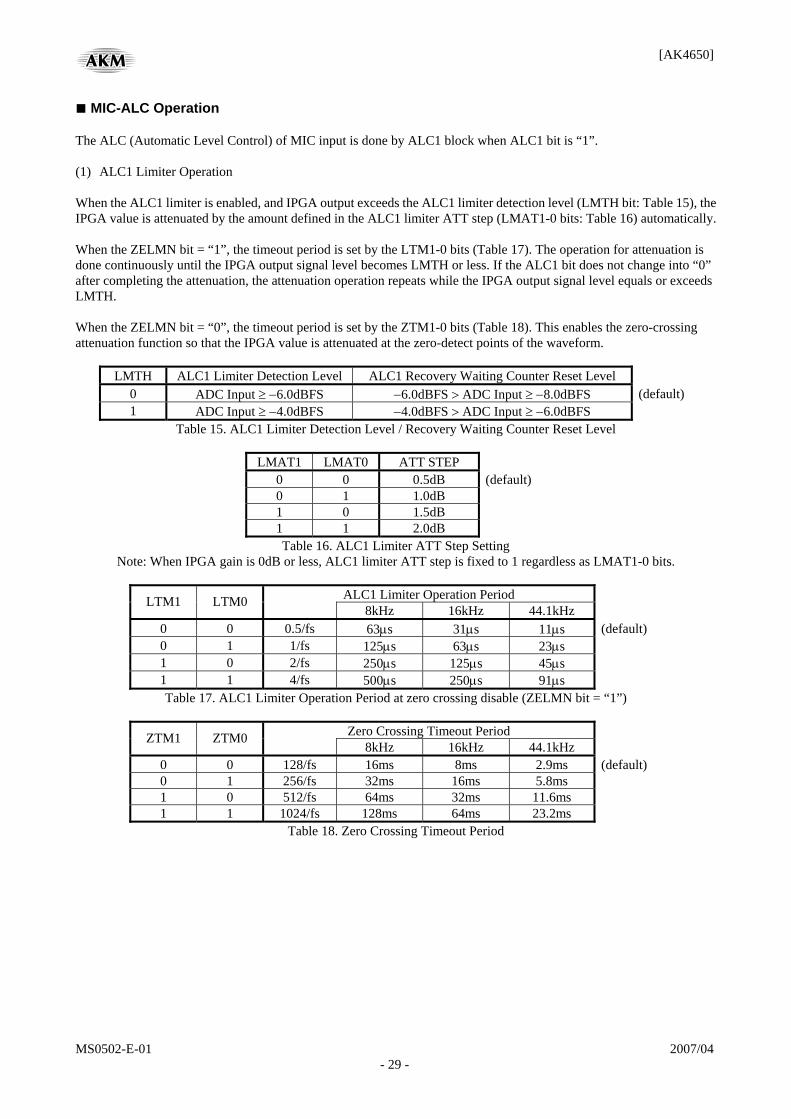
■ MIC-ALC Operation The ALC (Automatic Level Control) of MIC input is done by ALC1 block when ALC1 bit is “1”. (1) ALC1 Limiter Operation When the ALC1 limiter is enabled, and IPGA output exceeds the ALC1 limiter detection level (LMTH bit: Table 15), the IPGA value is attenuated by the amount defined in the ALC1 limiter ATT step (LMAT1-0 bits: Table 16) automatically. When the ZELMN bit = “1”, the timeout period is set by the LTM1-0 bits (Table 17). The operation for attenuation is done continuously until the IPGA output signal level becomes LMTH or less. If the ALC1 bit does not change into “0” after completing the attenuation, the attenuation operation repeats while the IPGA output signal level equals or exceeds LMTH. When the ZELMN bit = “0”, the timeout period is set by the ZTM1-0 bits (Table 18). This enables the zero-crossing attenuation function so that the IPGA value is attenuated at the zero-detect points of the waveform.
LMTH ALC1 Limiter Detection Level ALC1 Recovery Waiting Counter Reset Level 0 ADC Input ≥ −6.0dBFS −6.0dBFS > ADC Input ≥ −8.0dBFS (default)1 ADC Input ≥ −4.0dBFS −4.0dBFS > ADC Input ≥ −6.0dBFS
Table 15. ALC1 Limiter Detection Level / Recovery Waiting Counter Reset Level
LMAT1 LMAT0 ATT STEP 0 0 0.5dB (default) 0 1 1.0dB 1 0 1.5dB 1 1 2.0dB Table 16. ALC1 Limiter ATT Step Setting
Note: When IPGA gain is 0dB or less, ALC1 limiter ATT step is fixed to 1 regardless as LMAT1-0 bits.
ALC1 Limiter Operation Period LTM1 LTM0 8kHz 16kHz 44.1kHz
0 0 0.5/fs 63μs 31μs 11μs (default) 0 1 1/fs 125μs 63μs 23μs 1 0 2/fs 250μs 125μs 45μs 1 1 4/fs 500μs 250μs 91μs Table 17. ALC1 Limiter Operation Period at zero crossing disable (ZELMN bit = “1”)
Zero Crossing Timeout Period ZTM1 ZTM0
8kHz 16kHz 44.1kHz 0 0 128/fs 16ms 8ms 2.9ms (default) 0 1 256/fs 32ms 16ms 5.8ms 1 0 512/fs 64ms 32ms 11.6ms 1 1 1024/fs 128ms 64ms 23.2ms
Table 18. Zero Crossing Timeout Period
[AK4650]
MS0502-E-01 2007/04 - 30 -
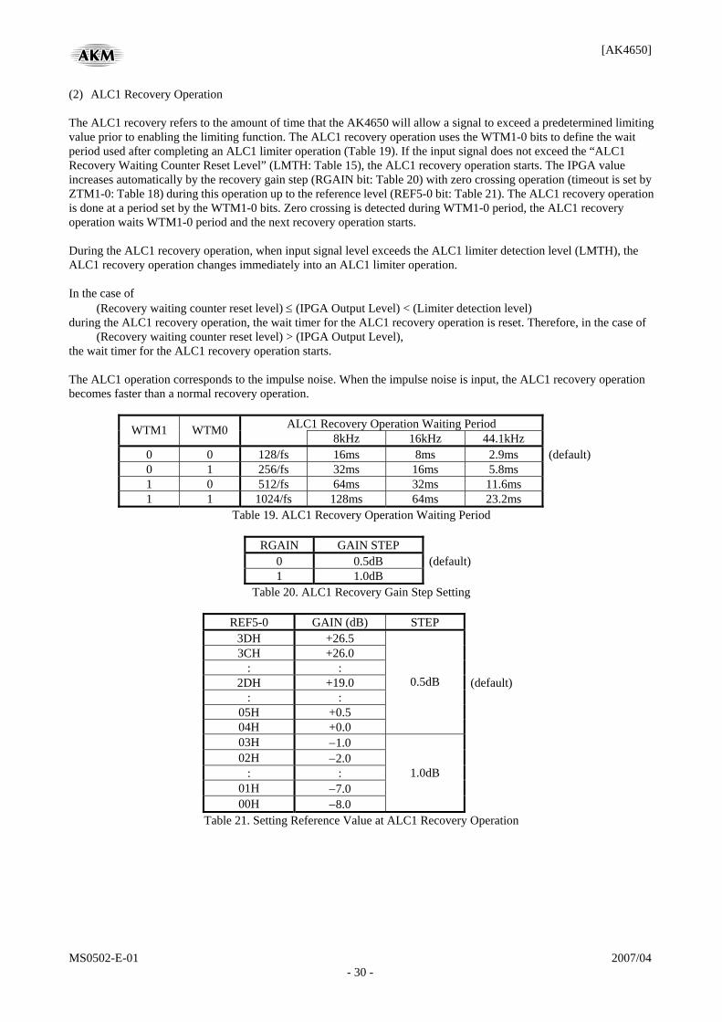
(2) ALC1 Recovery Operation The ALC1 recovery refers to the amount of time that the AK4650 will allow a signal to exceed a predetermined limiting value prior to enabling the limiting function. The ALC1 recovery operation uses the WTM1-0 bits to define the wait period used after completing an ALC1 limiter operation (Table 19). If the input signal does not exceed the “ALC1 Recovery Waiting Counter Reset Level” (LMTH: Table 15), the ALC1 recovery operation starts. The IPGA value increases automatically by the recovery gain step (RGAIN bit: Table 20) with zero crossing operation (timeout is set by ZTM1-0: Table 18) during this operation up to the reference level (REF5-0 bit: Table 21). The ALC1 recovery operation is done at a period set by the WTM1-0 bits. Zero crossing is detected during WTM1-0 period, the ALC1 recovery operation waits WTM1-0 period and the next recovery operation starts. During the ALC1 recovery operation, when input signal level exceeds the ALC1 limiter detection level (LMTH), the ALC1 recovery operation changes immediately into an ALC1 limiter operation. In the case of
(Recovery waiting counter reset level) ≤ (IPGA Output Level) < (Limiter detection level) during the ALC1 recovery operation, the wait timer for the ALC1 recovery operation is reset. Therefore, in the case of
(Recovery waiting counter reset level) > (IPGA Output Level), the wait timer for the ALC1 recovery operation starts. The ALC1 operation corresponds to the impulse noise. When the impulse noise is input, the ALC1 recovery operation becomes faster than a normal recovery operation.
ALC1 Recovery Operation Waiting Period WTM1 WTM0 8kHz 16kHz 44.1kHz
0 0 128/fs 16ms 8ms 2.9ms (default) 0 1 256/fs 32ms 16ms 5.8ms 1 0 512/fs 64ms 32ms 11.6ms 1 1 1024/fs 128ms 64ms 23.2ms
Table 19. ALC1 Recovery Operation Waiting Period
RGAIN GAIN STEP 0 0.5dB (default)1 1.0dB
Table 20. ALC1 Recovery Gain Step Setting
REF5-0 GAIN (dB) STEP 3DH +26.5 3CH +26.0
: : 2DH +19.0 (default)
: : 05H +0.5 04H +0.0
0.5dB
03H −1.0 02H −2.0
: : 01H −7.0 00H −8.0
1.0dB
Table 21. Setting Reference Value at ALC1 Recovery Operation
[AK4650]
MS0502-E-01 2007/04 - 31 -
(3) Example of ALC1 Operation Table 22 shows the examples of the ALC1 setting. In case of this examples, ALC1 operation starts from 0dB.
fs=8kHz fs=16kHz fs=44.1kHz Register Name Comment
Data Operation Data Operation Data OperationLMTH Limiter detection Level 1 −4dBFS 1 −4dBFS 1 −4dBFS LTM1-0 Limiter operation period at ZELMN
bit = “1” 00 Don’t use 00 Don’t use 00 Don’t use
ZELMN Limiter zero crossing detection 0 Enable 0 Enable 0 Enable ZTM1-0 Zero crossing timeout period 00 16ms 01 16ms 10 11.6ms
WTM1-0 Recovery waiting period *WTM1-0 bits should be the same
data as ZTM1-0 bits 00 16ms 01 16ms 10 11.6ms
REF5-0 Maximum gain at recovery operation 3DH +26.5dB 3DH +26.5dB 3DH +26.5dB IPGA5-0 Gain of IPGA at ALC1 operation start 37H 0dB 37H 0dB 37H 0dB LMAT1-0 Limiter ATT Step 00 0.5dB 00 0.5dB 00 0.5dB RGAIN Recovery GAIN Step 0 0.5dB 0 0.5dB 0 0.5dB ALC1 ALC1 Enable bit 1 Enable 1 Enable 1 Enable
Table 22. Example of the ALC1 setting The following registers should not be changed during the ALC1 operation. These bits should be changed, after the ALC1 operation is finished by ALC1 bit = “0” or PMMIC bit = “0”.
• LTM1-0, LMTH, LMAT1-0, WTM1-0, ZTM1-0, RGAIN, REF5-0, ZELMN bits IPGA gain at ALC1 operation start can be changed from the default value of IPGA5-0 bits while PMMIC bit is “1” and ALC1 bit is “0”. When ALC1 bit is changed from “1” to “0”, IPGA holds the last gain value set by ALC1 operation.
Manual Mode
* The value of IPGA should be
the same or smaller than REF’s
WR (ZTM1-0, WTM1-0, LTM1-0)
WR (REF5-0)
WR (IPGA5-0)
ALC1 Operation
WR (ALC1= “1”, LMAT1-0, RGAIN, LMTH, ZELMN)
Example:
Limiter = Zero crossing Enable
Recovery Cycle = 16ms @ fs= 8kHz
Limiter and Recovery Step = 0.5dB
Maximum Gain = +26.5dB
Limiter Detection Level = −4dBFS ALC bit = “1”
(1) Addr=66H, Data=4100H
(2) Addr=64H, Data=3D31H
(4) Addr=66H, Data=6100H
(3) Addr=0EH, Data=0077H
Note : WR : Write
Figure 19. Registers set-up sequence at ALC1 operation
[AK4650]
MS0502-E-01 2007/04 - 32 -
■ De-emphasis Filter The AK4650 includes the digital de-emphasis filter (tc = 50/15μs) by IIR filter. Setting the DEM1-0 bits enables the de-emphasis filter (Table 23).
DEM1 DEM0 Mode 0 0 44.1kHz 0 1 OFF (default)1 0 48kHz 1 1 32kHz
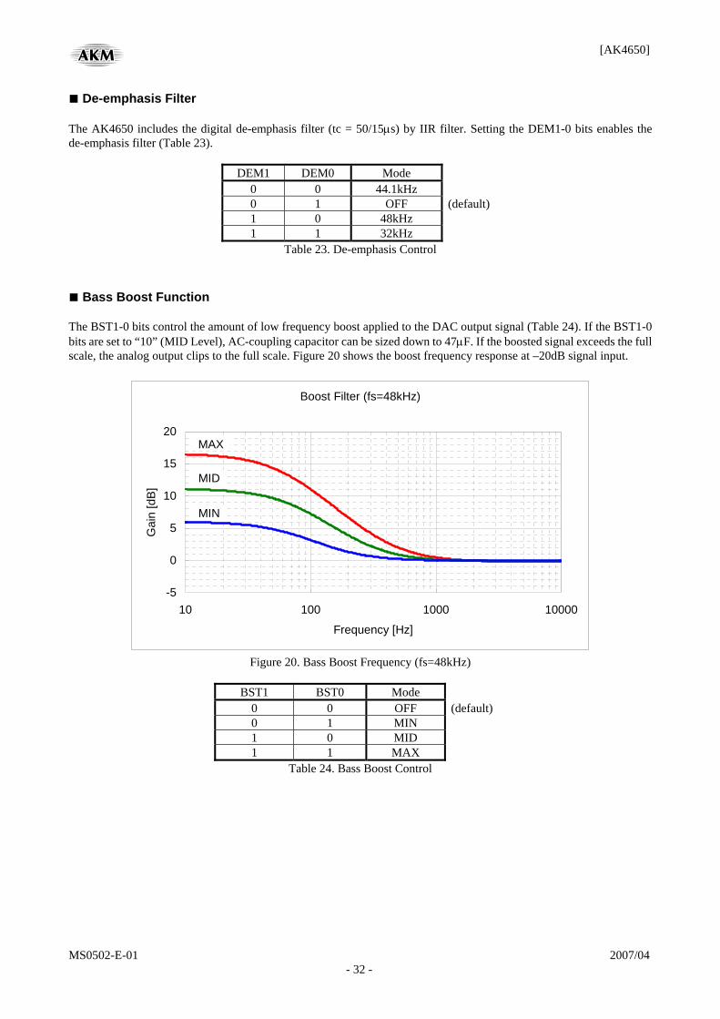
Table 23. De-emphasis Control ■ Bass Boost Function The BST1-0 bits control the amount of low frequency boost applied to the DAC output signal (Table 24). If the BST1-0 bits are set to “10” (MID Level), AC-coupling capacitor can be sized down to 47μF. If the boosted signal exceeds the full scale, the analog output clips to the full scale. Figure 20 shows the boost frequency response at –20dB signal input.
Boost Filter (fs=48kHz)
-5
0
5
10
15
20
10 100 1000 10000
Frequency [Hz]
Gai
n [d
B]
MAX
MID
MIN
Figure 20. Bass Boost Frequency (fs=48kHz)
BST1 BST0 Mode
0 0 OFF (default) 0 1 MIN 1 0 MID 1 1 MAX
Table 24. Bass Boost Control
[AK4650]
MS0502-E-01 2007/04 - 33 -
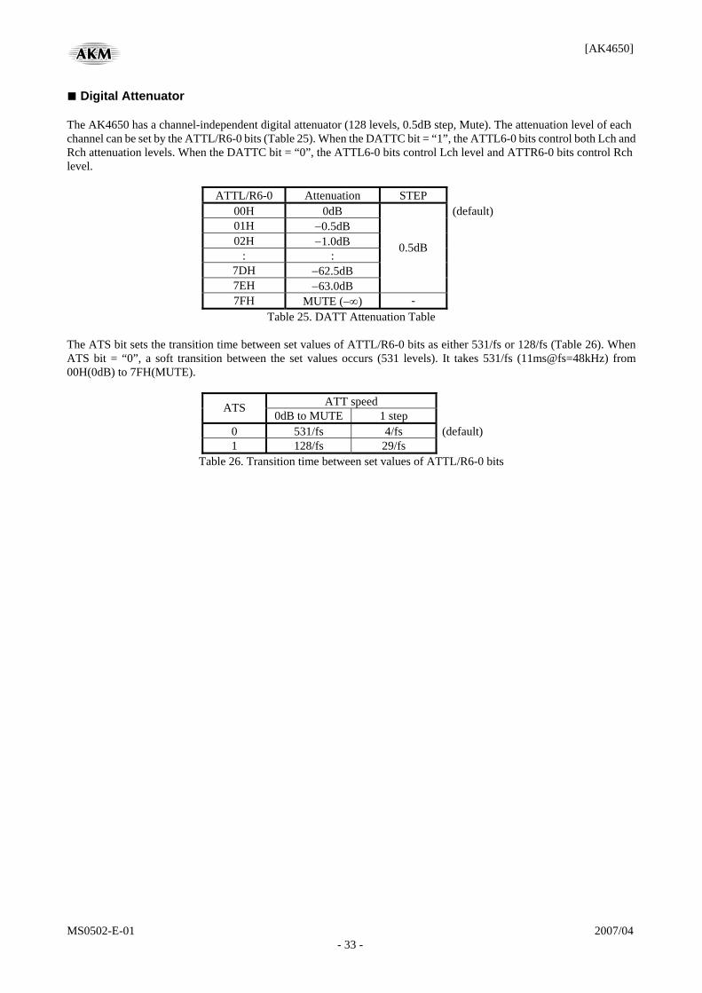
■ Digital Attenuator The AK4650 has a channel-independent digital attenuator (128 levels, 0.5dB step, Mute). The attenuation level of each channel can be set by the ATTL/R6-0 bits (Table 25). When the DATTC bit = “1”, the ATTL6-0 bits control both Lch and Rch attenuation levels. When the DATTC bit = “0”, the ATTL6-0 bits control Lch level and ATTR6-0 bits control Rch level.
ATTL/R6-0 Attenuation STEP 00H 0dB (default)01H −0.5dB 02H −1.0dB
: : 7DH −62.5dB 7EH −63.0dB
0.5dB
7FH MUTE (−∞) -
Table 25. DATT Attenuation Table The ATS bit sets the transition time between set values of ATTL/R6-0 bits as either 531/fs or 128/fs (Table 26). When ATS bit = “0”, a soft transition between the set values occurs (531 levels). It takes 531/fs (11ms@fs=48kHz) from 00H(0dB) to 7FH(MUTE).
ATT speed ATS 0dB to MUTE 1 step
0 531/fs 4/fs (default) 1 128/fs 29/fs
Table 26. Transition time between set values of ATTL/R6-0 bits
[AK4650]
MS0502-E-01 2007/04 - 34 -
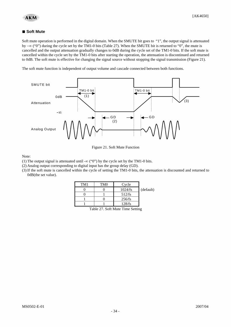
■ Soft Mute Soft mute operation is performed in the digital domain. When the SMUTE bit goes to “1”, the output signal is attenuated by −∞ (“0”) during the cycle set by the TM1-0 bits (Table 27). When the SMUTE bit is returned to “0”, the mute is cancelled and the output attenuation gradually changes to 0dB during the cycle set of the TM1-0 bits. If the soft mute is cancelled within the cycle set by the TM1-0 bits after starting the operation, the attenuation is discontinued and returned to 0dB. The soft mute is effective for changing the signal source without stopping the signal transmission (Figure 21). The soft mute function is independent of output volume and cascade connected between both functions.
SMUTE bit
Attenuation
TM1-0 bit
0dB
-∞
TM1-0 bit
GD GD
(1)
(2)
(3)
Analog Output
Figure 21. Soft Mute Function Note: (1) The output signal is attenuated until -∞ (“0”) by the cycle set by the TM1-0 bits. (2) Analog output corresponding to digital input has the group delay (GD). (3) If the soft mute is cancelled within the cycle of setting the TM1-0 bits, the attenuation is discounted and returned to
0dB(the set value).
TM1 TM0 Cycle 0 0 1024/fs (default)0 1 512/fs 1 0 256/fs 1 1 128/fs
Table 27. Soft Mute Time Setting
[AK4650]
MS0502-E-01 2007/04 - 35 -
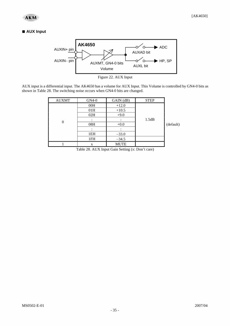
■ AUX Input
AUXMT, GN4-0 bits
AUXIN+ pin
AUXIN− pinAUXL bit
AUXAD bitADC
HP, SP
Volume
AK4650
Figure 22. AUX Input
AUX input is a differential input. The AK4650 has a volume for AUX Input. This Volume is controlled by GN4-0 bits as shown in Table 28. The switching noise occurs when GN4-0 bits are changed.
AUXMT GN4-0 GAIN (dB) STEP 00H +12.0 01H +10.5 02H +9.0
: : 08H +0.0 (default)
: : 1EH −33.0
1.5dB
0
1FH −34.5 1 x MUTE
Table 28. AUX Input Gain Setting (x: Don’t care)
[AK4650]
MS0502-E-01 2007/04 - 36 -
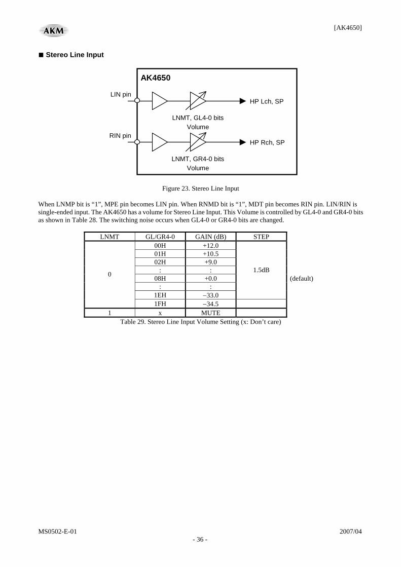
■ Stereo Line Input
HP Lch, SP
Volume
LIN pin
LNMT, GL4-0 bits
AK4650
HP Rch, SP
Volume
RIN pin
LNMT, GR4-0 bits
Figure 23. Stereo Line Input When LNMP bit is “1”, MPE pin becomes LIN pin. When RNMD bit is “1”, MDT pin becomes RIN pin. LIN/RIN is single-ended input. The AK4650 has a volume for Stereo Line Input. This Volume is controlled by GL4-0 and GR4-0 bits as shown in Table 28. The switching noise occurs when GL4-0 or GR4-0 bits are changed.
LNMT GL/GR4-0 GAIN (dB) STEP 00H +12.0 01H +10.5 02H +9.0
: : 08H +0.0 (default)
: : 1EH −33.0
1.5dB
0
1FH −34.5 1 x MUTE
Table 29. Stereo Line Input Volume Setting (x: Don’t care)
[AK4650]
MS0502-E-01 2007/04 - 37 -
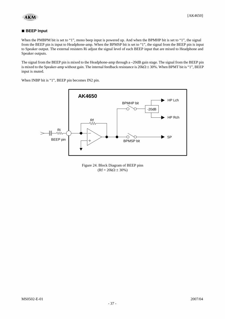
■ BEEP Input When the PMBPM bit is set to “1”, mono beep input is powered up. And when the BPMHP bit is set to “1”, the signal from the BEEP pin is input to Headphone-amp. When the BPMSP bit is set to “1”, the signal from the BEEP pin is input to Speaker output. The external resisters Ri adjust the signal level of each BEEP input that are mixed to Headphone and Speaker outputs. The signal from the BEEP pin is mixed to the Headphone-amp through a –20dB gain stage. The signal from the BEEP pin is mixed to the Speaker-amp without gain. The internal feedback resistance is 20kΩ ± 30%. When BPMT bit is “1”, BEEP input is muted. When INBP bit is “1”, BEEP pin becomes IN2 pin.
AK4650
BEEP pin
Ri
Rf
BPMHP bit
SP
-20dB
BPMSP bit
HP Lch
HP Rch
Figure 24. Block Diagram of BEEP pins (Rf = 20kΩ ± 30%)
[AK4650]
MS0502-E-01 2007/04 - 38 -
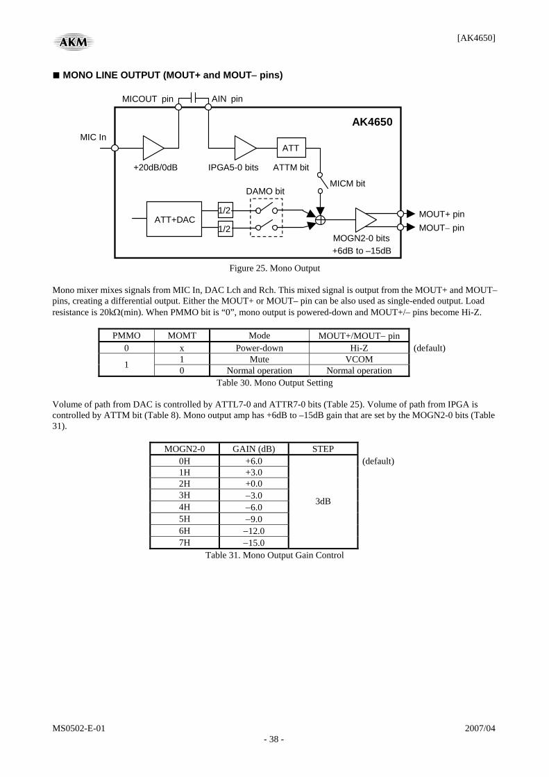
■ MONO LINE OUTPUT (MOUT+ and MOUT− pins)
ATT+DAC
MIC In
+20dB/0dB IPGA5-0 bits
MOUT+ pin
1/2 MOUT− pin
+6dB to –15dB
1/2
MICM bitDAMO bit
MOGN2-0 bits
ATT
AK4650
MICOUT pin AIN pin
ATTM bit
Figure 25. Mono Output
Mono mixer mixes signals from MIC In, DAC Lch and Rch. This mixed signal is output from the MOUT+ and MOUT– pins, creating a differential output. Either the MOUT+ or MOUT– pin can be also used as single-ended output. Load resistance is 20kΩ(min). When PMMO bit is “0”, mono output is powered-down and MOUT+/– pins become Hi-Z.
PMMO MOMT Mode MOUT+/MOUT− pin 0 x Power-down Hi-Z (default)
1 Mute VCOM 1 0 Normal operation Normal operation Table 30. Mono Output Setting
Volume of path from DAC is controlled by ATTL7-0 and ATTR7-0 bits (Table 25). Volume of path from IPGA is controlled by ATTM bit (Table 8). Mono output amp has +6dB to –15dB gain that are set by the MOGN2-0 bits (Table 31).
MOGN2-0 GAIN (dB) STEP 0H +6.0 (default) 1H +3.0 2H +0.0 3H −3.0 4H −6.0 5H −9.0 6H −12.0 7H −15.0
3dB
Table 31. Mono Output Gain Control
[AK4650]
MS0502-E-01 2007/04 - 39 -
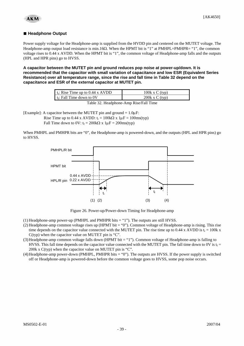
■ Headphone Output Power supply voltage for the Headphone-amp is supplied from the HVDD pin and centered on the MUTET voltage. The Headphone-amp output load resistance is min.16Ω. When the HPMT bit is “1” at PMHPL=PMHPR= “1”, the common voltage rises to 0.44 x AVDD. When the HPMT bit is “1”, the common voltage of Headphone-amp falls and the outputs (HPL and HPR pins) go to HVSS. A capacitor between the MUTET pin and ground reduces pop noise at power-up/down. It is recommended that the capacitor with small variation of capacitance and low ESR (Equivalent Series Resistance) over all temperature range, since the rise and fall time in Table 32 depend on the capacitance and ESR of the external capacitor at MUTET pin.
tr: Rise Time up to 0.44 x AVDD 100k x C (typ) tf: Fall Time down to 0V 200k x C (typ)
Table 32. Headphone-Amp Rise/Fall Time [Example]: A capacitor between the MUTET pin and ground = 1.0μF:
Rise Time up to 0.44 x AVDD: tr = 100kΩ x 1μF = 100ms(typ) Fall Time down to 0V: tf = 200kΩ x 1μF = 200ms(typ)
When PMHPL and PMHPR bits are “0”, the Headphone-amp is powered-down, and the outputs (HPL and HPR pins) go to HVSS.
HPMT bit
PMHPL/R bit
HPL/R pin
(1) (2) (4)(3)
tr tf
0.22 x AVDD 0.44 x AVDD
Figure 26. Power-up/Power-down Timing for Headphone-amp (1) Headphone-amp power-up (PMHPL and PMHPR bits = “1”). The outputs are still HVSS. (2) Headphone-amp common voltage rises up (HPMT bit = “0”). Common voltage of Headphone-amp is rising. This rise
time depends on the capacitor value connected with the MUTET pin. The rise time up to 0.44 x AVDD is tr = 100k x C(typ) when the capacitor value on MUTET pin is “C”.
(3) Headphone-amp common voltage falls down (HPMT bit = “1”). Common voltage of Headphone-amp is falling to HVSS. This fall time depends on the capacitor value connected with the MUTET pin. The fall time down to 0V is tf = 200k x C(typ) when the capacitor value on MUTET pin is “C”.
(4) Headphone-amp power-down (PMHPL, PMHPR bits = “0”). The outputs are HVSS. If the power supply is switched off or Headphone-amp is powered-down before the common voltage goes to HVSS, some pop noise occurs.

[AK4650]
MS0502-E-01 2007/04 - 40 -
The cut-off frequency of Headphone-amp output depends on the external resistor and capacitor used. Table 33 shows the cut off frequency and the output power for various resistor/capacitor combinations. The Headphone impedance RL is 16Ω. Output powers are shown at HVDD = 2.7, 3.0 and 3.3V. The output voltage of Headphone is 0.6 x AVDD (Vpp).
AK4650
HP-AMP
16Ω
HeadphoneR C
Figure 27. External Circuit Example of Headphone
Output Power [mW] R [Ω] C [μF] fc [Hz]
BOOST=OFF fc [Hz]
BOOST=MIN 2.7V 3.0V 3.3V 220 45.2 17 0 100 99.5 42
27.9 34.5 41.7
100 69.8 28 6.8 47 148.5 74
13.7 17.0 20.5
100 49.7 19 16 47 105.8 46
7.0 8.6 10.4
Table 33. Relationship of external circuit, output power and frequency response
[AK4650]
MS0502-E-01 2007/04 - 41 -
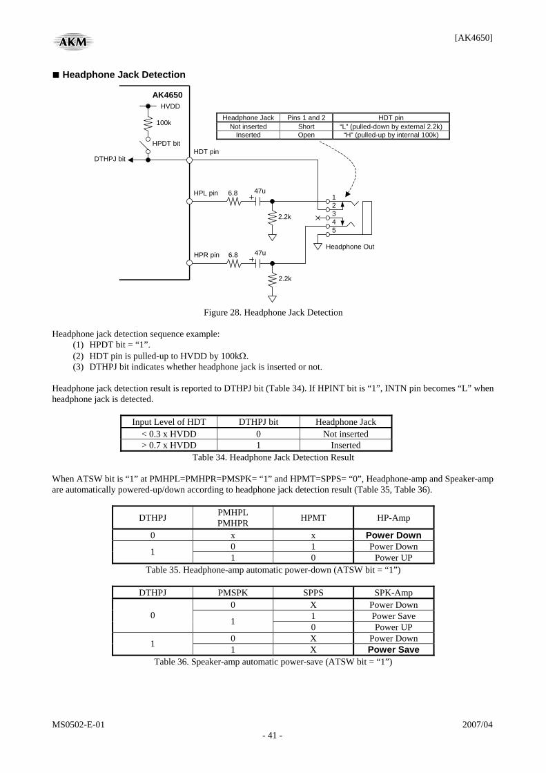
■ Headphone Jack Detection
HPL pin 6.8
2.2k
47u
HPR pin 6.8
2.2k
47u
AK4650
100k
HVDD
Headphone Out
1 2 3 4 5
HDT pin
Headphone Jack Pins 1 and 2 HDT pin Not inserted Short “L” (pulled-down by external 2.2k)
Inserted Open “H” (pulled-up by internal 100k) HPDT bit
DTHPJ bit
Figure 28. Headphone Jack Detection
Headphone jack detection sequence example:
(1) HPDT bit = “1”. (2) HDT pin is pulled-up to HVDD by 100kΩ. (3) DTHPJ bit indicates whether headphone jack is inserted or not.
Headphone jack detection result is reported to DTHPJ bit (Table 34). If HPINT bit is “1”, INTN pin becomes “L” when headphone jack is detected.
Input Level of HDT DTHPJ bit Headphone Jack < 0.3 x HVDD 0 Not inserted > 0.7 x HVDD 1 Inserted
Table 34. Headphone Jack Detection Result When ATSW bit is “1” at PMHPL=PMHPR=PMSPK= “1” and HPMT=SPPS= “0”, Headphone-amp and Speaker-amp are automatically powered-up/down according to headphone jack detection result (Table 35, Table 36).
DTHPJ PMHPL PMHPR HPMT HP-Amp
0 x x Power Down 0 1 Power Down 1 1 0 Power UP
Table 35. Headphone-amp automatic power-down (ATSW bit = “1”)
DTHPJ PMSPK SPPS SPK-Amp 0 X Power Down
1 Power Save 0 1 0 Power UP 0 X Power Down 1 1 X Power Save
Table 36. Speaker-amp automatic power-save (ATSW bit = “1”)
[AK4650]
MS0502-E-01 2007/04 - 42 -
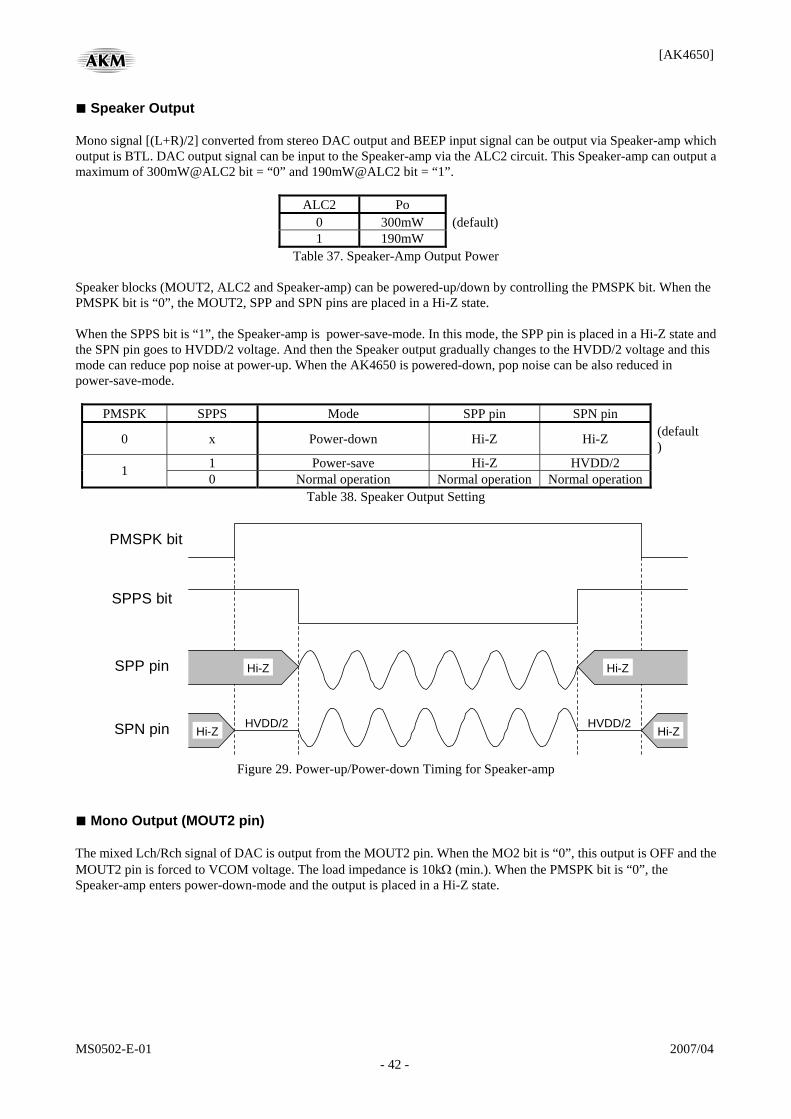
■ Speaker Output Mono signal [(L+R)/2] converted from stereo DAC output and BEEP input signal can be output via Speaker-amp which output is BTL. DAC output signal can be input to the Speaker-amp via the ALC2 circuit. This Speaker-amp can output a maximum of 300mW@ALC2 bit = “0” and 190mW@ALC2 bit = “1”.
ALC2 Po 0 300mW (default) 1 190mW
Table 37. Speaker-Amp Output Power Speaker blocks (MOUT2, ALC2 and Speaker-amp) can be powered-up/down by controlling the PMSPK bit. When the PMSPK bit is “0”, the MOUT2, SPP and SPN pins are placed in a Hi-Z state. When the SPPS bit is “1”, the Speaker-amp is power-save-mode. In this mode, the SPP pin is placed in a Hi-Z state and the SPN pin goes to HVDD/2 voltage. And then the Speaker output gradually changes to the HVDD/2 voltage and this mode can reduce pop noise at power-up. When the AK4650 is powered-down, pop noise can be also reduced in power-save-mode.
PMSPK SPPS Mode SPP pin SPN pin
0 x Power-down Hi-Z Hi-Z (default)
1 Power-save Hi-Z HVDD/2 1 0 Normal operation Normal operation Normal operation Table 38. Speaker Output Setting
PMSPK bit
SPPS bit
SPP pin
SPN pin HVDD/2 HVDD/2
Hi-Z Hi-Z
Hi-Z Hi-Z
Figure 29. Power-up/Power-down Timing for Speaker-amp
■ Mono Output (MOUT2 pin) The mixed Lch/Rch signal of DAC is output from the MOUT2 pin. When the MO2 bit is “0”, this output is OFF and the MOUT2 pin is forced to VCOM voltage. The load impedance is 10kΩ (min.). When the PMSPK bit is “0”, the Speaker-amp enters power-down-mode and the output is placed in a Hi-Z state.
[AK4650]
MS0502-E-01 2007/04 - 43 -
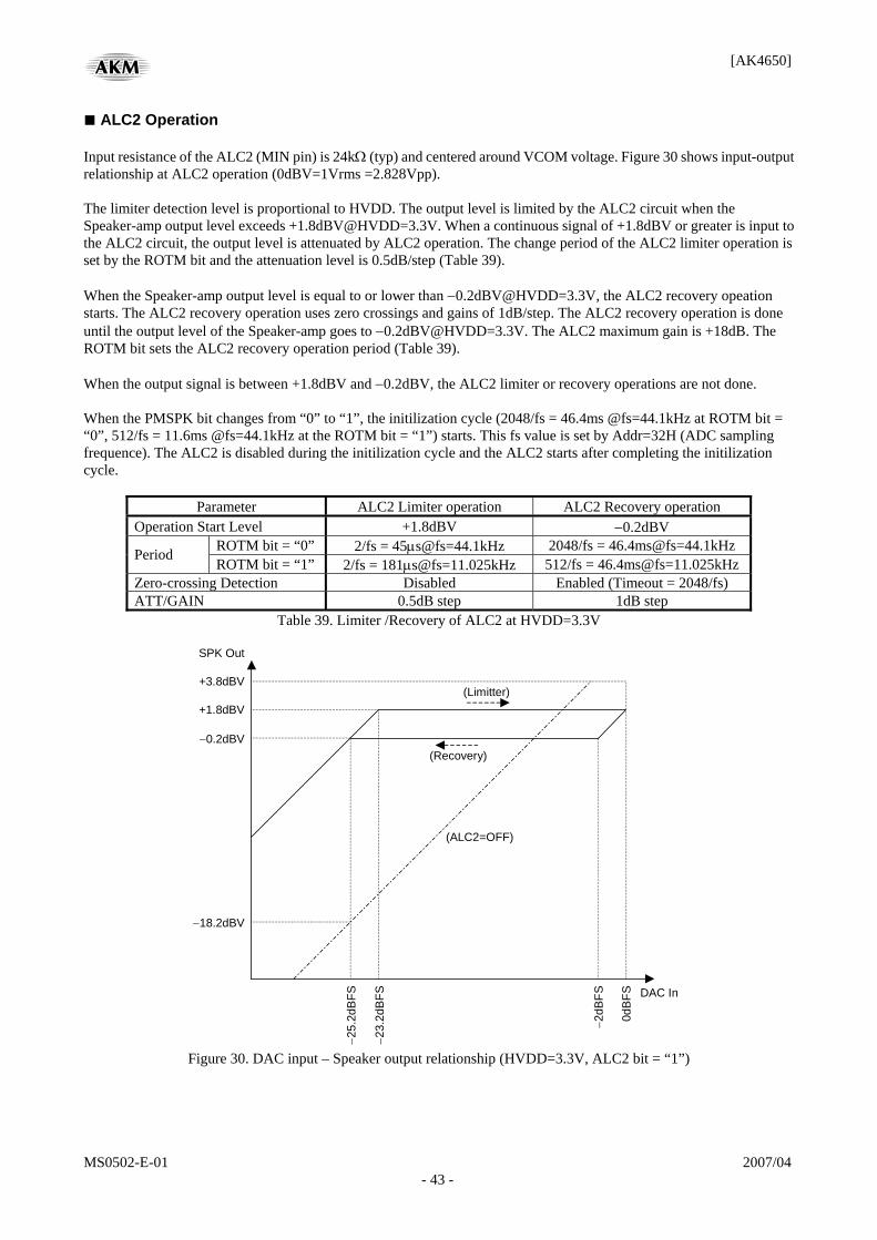
■ ALC2 Operation Input resistance of the ALC2 (MIN pin) is 24kΩ (typ) and centered around VCOM voltage. Figure 30 shows input-output relationship at ALC2 operation (0dBV=1Vrms =2.828Vpp). The limiter detection level is proportional to HVDD. The output level is limited by the ALC2 circuit when the Speaker-amp output level exceeds +1.8dBV@HVDD=3.3V. When a continuous signal of +1.8dBV or greater is input to the ALC2 circuit, the output level is attenuated by ALC2 operation. The change period of the ALC2 limiter operation is set by the ROTM bit and the attenuation level is 0.5dB/step (Table 39). When the Speaker-amp output level is equal to or lower than −0.2dBV@HVDD=3.3V, the ALC2 recovery opeation starts. The ALC2 recovery operation uses zero crossings and gains of 1dB/step. The ALC2 recovery operation is done until the output level of the Speaker-amp goes to −0.2dBV@HVDD=3.3V. The ALC2 maximum gain is +18dB. The ROTM bit sets the ALC2 recovery operation period (Table 39). When the output signal is between +1.8dBV and −0.2dBV, the ALC2 limiter or recovery operations are not done. When the PMSPK bit changes from “0” to “1”, the initilization cycle (2048/fs = 46.4ms @fs=44.1kHz at ROTM bit = “0”, 512/fs = 11.6ms @fs=44.1kHz at the ROTM bit = “1”) starts. This fs value is set by Addr=32H (ADC sampling frequence). The ALC2 is disabled during the initilization cycle and the ALC2 starts after completing the initilization cycle.
Parameter ALC2 Limiter operation ALC2 Recovery operation Operation Start Level +1.8dBV −0.2dBV
ROTM bit = “0” 2/fs = 45μs@fs=44.1kHz 2048/fs = 46.4ms@fs=44.1kHz Period ROTM bit = “1” 2/fs = 181μs@fs=11.025kHz 512/fs = 46.4ms@fs=11.025kHz
Zero-crossing Detection Disabled Enabled (Timeout = 2048/fs) ATT/GAIN 0.5dB step 1dB step
Table 39. Limiter /Recovery of ALC2 at HVDD=3.3V
SPK Out
DAC In
+1.8dBV
−0.2dBV
−25.
2dBF
S
−23.
2dBF
S
−2dB
FS
0dBF
S
+3.8dBV
(ALC2=OFF)
(Limitter)
(Recovery)
−18.2dBV
Figure 30. DAC input – Speaker output relationship (HVDD=3.3V, ALC2 bit = “1”)
[AK4650]
MS0502-E-01 2007/04 - 44 -
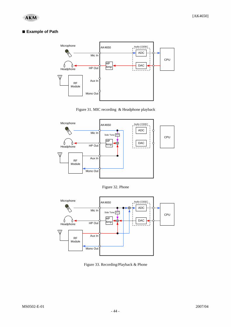
■ Example of Path
AK4650
ADC
DAC
RF Module
Mono Out
HPAmp
CPU
Audio CODEC
Aux In
HP Out
Mic In
Headphone
Microphone
Figure 31. MIC recording & Headphone playback
AK4650
ADC
DAC
RF Module
Mono Out
HPAmp
CPU
Audio CODEC
Aux In
HP Out
Mic In
Headphone
Microphone
ATTSide Tone
Figure 32. Phone
AK4650
ADC
DAC
RF Module
Mono Out
HPAmp
CPU
Audio CODEC
Aux In
HP Out
Mic In
Headphone
Microphone
ATTSide Tone
Figure 33. Recording/Playback & Phone
[AK4650]
MS0502-E-01 2007/04 - 45 -
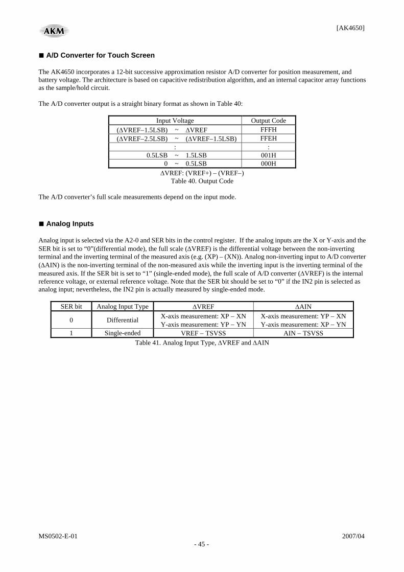
■ A/D Converter for Touch Screen The AK4650 incorporates a 12-bit successive approximation resistor A/D converter for position measurement, and battery voltage. The architecture is based on capacitive redistribution algorithm, and an internal capacitor array functions as the sample/hold circuit. The A/D converter output is a straight binary format as shown in Table 40:
Input Voltage Output Code (ΔVREF−1.5LSB) ~ ΔVREF FFFH (ΔVREF−2.5LSB) ~ (ΔVREF−1.5LSB) FFEH
: : 0.5LSB ~ 1.5LSB 001H
0 ~ 0.5LSB 000H ΔVREF: (VREF+) – (VREF−)
Table 40. Output Code The A/D converter’s full scale measurements depend on the input mode. ■ Analog Inputs Analog input is selected via the A2-0 and SER bits in the control register. If the analog inputs are the X or Y-axis and the SER bit is set to “0”(differential mode), the full scale (ΔVREF) is the differential voltage between the non-inverting terminal and the inverting terminal of the measured axis (e.g. (XP) – (XN)). Analog non-inverting input to A/D converter (ΔAIN) is the non-inverting terminal of the non-measured axis while the inverting input is the inverting terminal of the measured axis. If the SER bit is set to “1” (single-ended mode), the full scale of A/D converter (ΔVREF) is the internal reference voltage, or external reference voltage. Note that the SER bit should be set to “0” if the IN2 pin is selected as analog input; nevertheless, the IN2 pin is actually measured by single-ended mode.
SER bit Analog Input Type ΔVREF ΔAIN
0 Differential X-axis measurement: XP − XN Y-axis measurement: YP − YN
X-axis measurement: YP − XN Y-axis measurement: XP − YN
1 Single-ended VREF − TSVSS AIN − TSVSS Table 41. Analog Input Type, ΔVREF and ΔAIN
[AK4650]
MS0502-E-01 2007/04 - 46 -
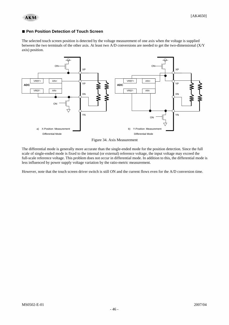
■ Pen Position Detection of Touch Screen The selected touch screen position is detected by the voltage measurement of one axis when the voltage is supplied between the two terminals of the other axis. At least two A/D conversions are needed to get the two-dimensional (X/Y axis) position.
YN
XN
YP
ON
VREF+
VREF-
ADC AIN+
AIN-
XP ON
a) X-Position Measurement
Differential Mode
b) Y-Position Measurement
Differential Mode
YN
XN
YP
ON
VREF+
VREF-
ADCAIN+
AIN-
XP ON
Figure 34. Axis Measurement
The differential mode is generally more accurate than the single-ended mode for the position detection. Since the full scale of single-ended mode is fixed to the internal (or external) reference voltage, the input voltage may exceed the full-scale reference voltage. This problem does not occur in differential mode. In addition to this, the differential mode is less influenced by power supply voltage variation by the ratio-metric measurement. However, note that the touch screen driver switch is still ON and the current flows even for the A/D conversion time.
[AK4650]
MS0502-E-01 2007/04 - 47 -
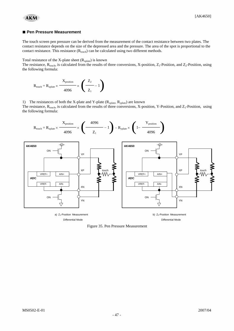
■ Pen Pressure Measurement The touch screen pen pressure can be derived from the measurement of the contact resistance between two plates. The contact resistance depends on the size of the depressed area and the pressure. The area of the spot is proportional to the contact resistance. This resistance (Rtouch) can be calculated using two different methods. Total resistance of the X-plate sheet (Rxplate) is known The resistance, Rtouch, is calculated from the results of three conversions, X-position, Z1-Position, and Z2-Position, using the following formula:
Rtouch = Rxplate × Xposition
4096 ×
Z2
Z1 ( – 1)
1) The resistances of both the X-plate and Y-plate (Rxplate, Ryplate) are known The resistance, Rtouch, is calculated from the results of three conversions, X-position, Y-Position, and Z1-Position, using the following formula:
Rtouch = Rxplate × Xposition
4096 ×
4096
Z1 ( – 1) – Ryplate ×
Yposition
4096 (1– )
ONYN
VREF+
VREF-
ADC AIN+
AIN-
XP
YP
XN
ON
a) Z1-Position Measurement
Differential Mode
touch
ONYN
VREF+
VREF-
ADCAIN+
AIN-
XP
YP
XN
ON
b) Z2-Position Measurement
Differential Mode
touch
AK4650 AK4650
Figure 35. Pen Pressure Measurement
[AK4650]
MS0502-E-01 2007/04 - 48 -
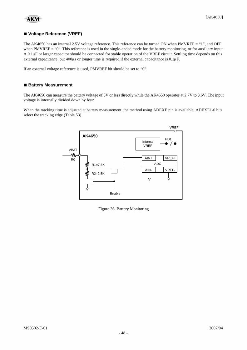
■ Voltage Reference (VREF) The AK4650 has an internal 2.5V voltage reference. This reference can be turned ON when PMVREF = “1”, and OFF when PMVREF = “0”. This reference is used in the single-ended mode for the battery monitoring, or for auxiliary input. A 0.1μF or larger capacitor should be connected for stable operation of the VREF circuit. Settling time depends on this external capacitance, but 400μs or longer time is required if the external capacitance is 0.1μF. If an external voltage reference is used, PMVREF bit should be set to “0”. ■ Battery Measurement The AK4650 can measure the battery voltage of 5V or less directly while the AK4650 operates at 2.7V to 3.6V. The input voltage is internally divided down by four. When the tracking time is adjusted at battery measurement, the method using ADEXE pin is available. ADEXE1-0 bits select the tracking edge (Table 53).
R1=7.5K
R2=2.5K
VBAT
ADC
Enable
R0 AIN+
AIN-
VREF+
VREF-
InternalVREF
PD1AK4650
VREF
Figure 36. Battery Monitoring
[AK4650]
MS0502-E-01 2007/04 - 49 -
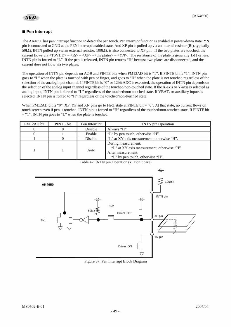
■ Pen Interrupt The AK4650 has pen interrupt function to detect the pen touch. Pen interrupt function is enabled at power-down state. YN pin is connected to GND at the PEN interrupt enabled state. And XP pin is pulled up via an internal resistor (Ri), typically 50kΩ. INTN pulled up via an external resistor, 100kΩ, is also connected to XP pin. If the two plates are touched, the current flows via <TSVDD> – <Ri> – <XP> –<the plates> – <YN>. The resistance of the plate is generally 1kΩ or less, INTN pin is forced to “L”. If the pen is released, INTN pin returns “H” because two plates are disconnected, and the current does not flow via two plates. The operation of INTN pin depends on A2-0 and PINTE bits when PM12AD bit is “1”. If PINTE bit is “1”, INTN pin goes to “L” when the plate is touched with pen or finger, and goes to “H” when the plate is not touched regardless of the selection of the analog input channel. If PINTE bit is “0” or 12bit ADC is executed, the operation of INTN pin depends on the selection of the analog input channel regardless of the touched/non-touched state. If the X-axis or Y-axis is selected as analog input, INTN pin is forced to “L” regardless of the touched/non-touched state. If VBAT, or auxiliary inputs is selected, INTN pin is forced to “H” regardless of the touched/non-touched state. When PM12AD bit is “0”, XP, YP and XN pins go to Hi-Z state at PINTE bit = “0”. At that state, no current flows on touch screen even if pen is touched. INTN pin is forced to “H” regardless of the touched/non-touched state. If PINTE bit = “1”, INTN pin goes to “L” when the plate is touched.
PM12AD bit PINTE bit Pen Interrupt INTN pin Operation 0 0 Disable Always “H”. 0 1 Enable “L” by pen touch, otherwise “H”. 1 0 Disable “L” at XY axis measurement, otherwise “H”.
1 1 Auto
During measurement: “L” at XY axis measurement, otherwise “H”.
After measurement: “L” by pen touch, otherwise “H”.
Table 42. INTN pin Operation (x: Don’t care)
XP pin
INTN pin
Driver ON
YN pin
100kΩ
EN2
50kΩDriver OFF
EN1
AK4650
Figure 37. Pen Interrupt Block Diagram
[AK4650]
MS0502-E-01 2007/04 - 50 -
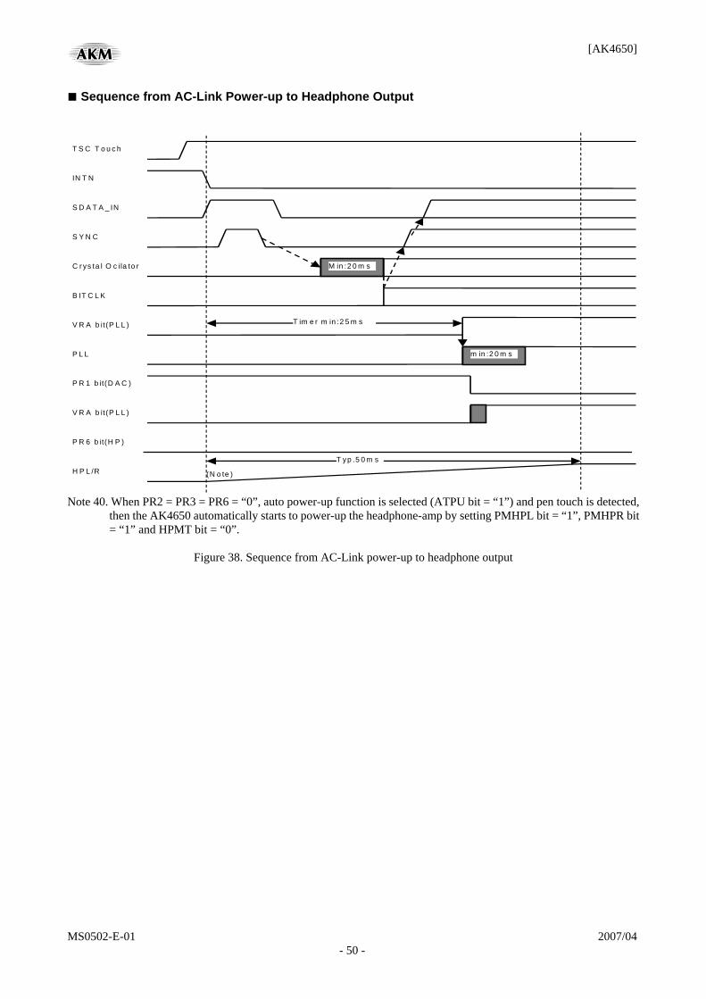
■ Sequence from AC-Link Power-up to Headphone Output
T S C T o u c h
IN T N
S D A T A _ IN
S Y N C
C r ys ta l O c ila to r
V R A b it(P L L )
B IT C L K
P L L
P R 1 b it(D A C )
V R A b it(P L L )
P R 6 b it(H P )
H P L /R T yp .5 0 m s
m in :2 0 m s
M in :2 0 m s
(N o te )
T im e r m in :2 5 m s
Note 40. When PR2 = PR3 = PR6 = “0”, auto power-up function is selected (ATPU bit = “1”) and pen touch is detected,
then the AK4650 automatically starts to power-up the headphone-amp by setting PMHPL bit = “1”, PMHPR bit = “1” and HPMT bit = “0”.
Figure 38. Sequence from AC-Link power-up to headphone output
[AK4650]
MS0502-E-01 2007/04 - 51 -
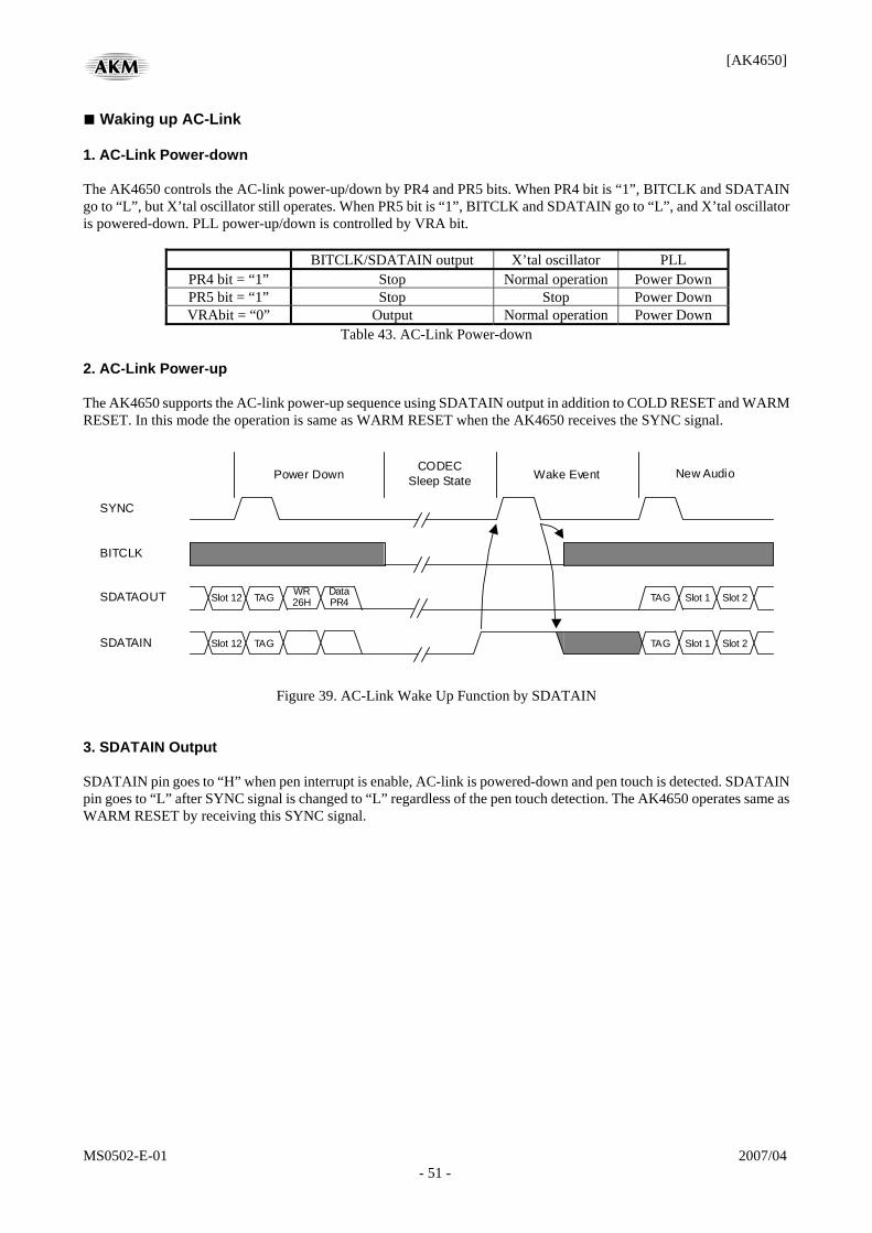
■ Waking up AC-Link 1. AC-Link Power-down The AK4650 controls the AC-link power-up/down by PR4 and PR5 bits. When PR4 bit is “1”, BITCLK and SDATAIN go to “L”, but X’tal oscillator still operates. When PR5 bit is “1”, BITCLK and SDATAIN go to “L”, and X’tal oscillator is powered-down. PLL power-up/down is controlled by VRA bit.
BITCLK/SDATAIN output X’tal oscillator PLL PR4 bit = “1” Stop Normal operation Power Down PR5 bit = “1” Stop Stop Power Down VRAbit = “0” Output Normal operation Power Down
Table 43. AC-Link Power-down 2. AC-Link Power-up The AK4650 supports the AC-link power-up sequence using SDATAIN output in addition to COLD RESET and WARM RESET. In this mode the operation is same as WARM RESET when the AK4650 receives the SYNC signal.
SYNC
BITCLK
SDATAOUT Slot 12 TAG WR 26H
Data PR4
SDATAIN Slot 12 TAG
TAG
TAG
Slot 1 Slot 2
Slot 1 Slot 2
Power Down CODEC
Sleep State Wake Event New Audio
Figure 39. AC-Link Wake Up Function by SDATAIN
3. SDATAIN Output SDATAIN pin goes to “H” when pen interrupt is enable, AC-link is powered-down and pen touch is detected. SDATAIN pin goes to “L” after SYNC signal is changed to “L” regardless of the pen touch detection. The AK4650 operates same as WARM RESET by receiving this SYNC signal.
[AK4650]
MS0502-E-01 2007/04 - 52 -
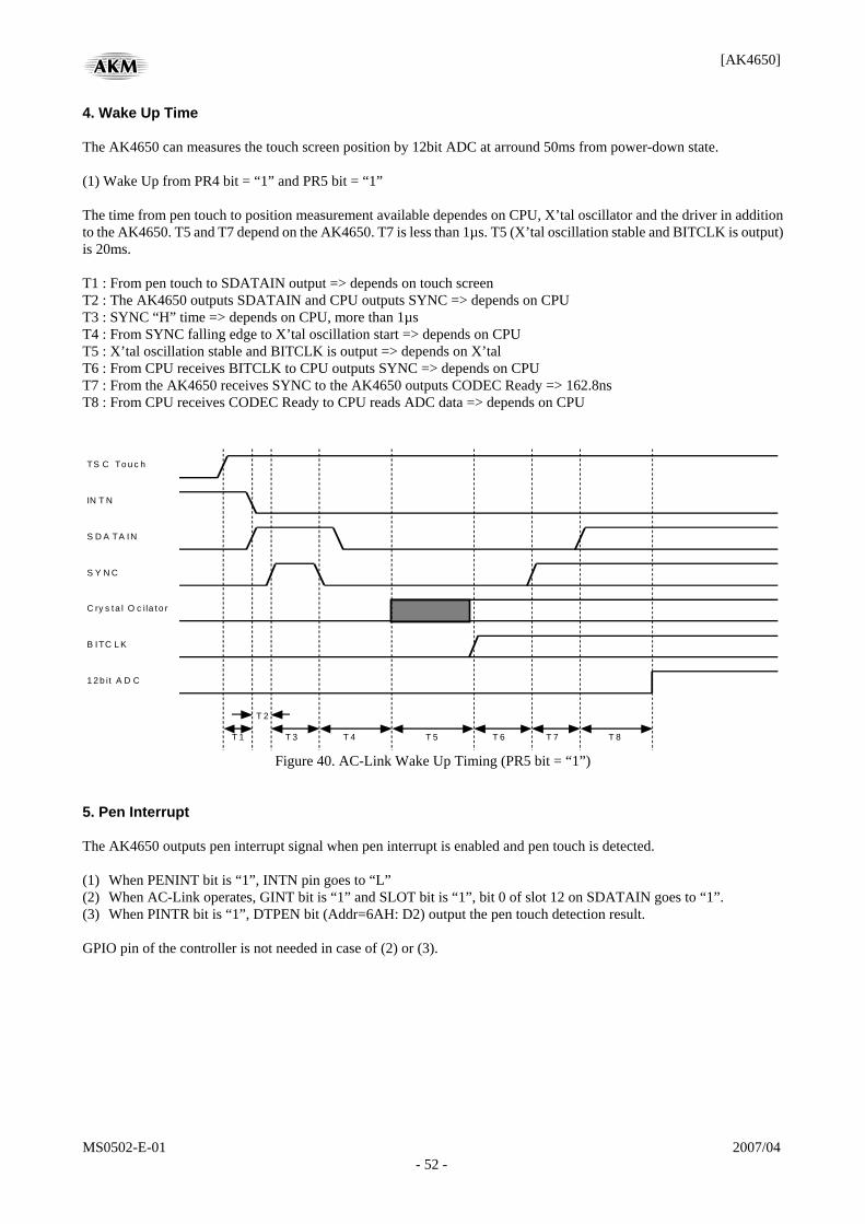
4. Wake Up Time The AK4650 can measures the touch screen position by 12bit ADC at arround 50ms from power-down state. (1) Wake Up from PR4 bit = “1” and PR5 bit = “1” The time from pen touch to position measurement available dependes on CPU, X’tal oscillator and the driver in addition to the AK4650. T5 and T7 depend on the AK4650. T7 is less than 1µs. T5 (X’tal oscillation stable and BITCLK is output) is 20ms. T1 : From pen touch to SDATAIN output => depends on touch screen T2 : The AK4650 outputs SDATAIN and CPU outputs SYNC => depends on CPU T3 : SYNC “H” time => depends on CPU, more than 1µs T4 : From SYNC falling edge to X’tal oscillation start => depends on CPU T5 : X’tal oscillation stable and BITCLK is output => depends on X’tal T6 : From CPU receives BITCLK to CPU outputs SYNC => depends on CPU T7 : From the AK4650 receives SYNC to the AK4650 outputs CODEC Ready => 162.8ns T8 : From CPU receives CODEC Ready to CPU reads ADC data => depends on CPU
TS C To u c h
IN T N
S D A TA IN
S Y N C
C ry s ta l O c ila to r
1 2 b it A D C
B ITC L K
T 2
T 3 T 4 T 5 T 6 T 7 T 8 T 1
Figure 40. AC-Link Wake Up Timing (PR5 bit = “1”) 5. Pen Interrupt The AK4650 outputs pen interrupt signal when pen interrupt is enabled and pen touch is detected. (1) When PENINT bit is “1”, INTN pin goes to “L” (2) When AC-Link operates, GINT bit is “1” and SLOT bit is “1”, bit 0 of slot 12 on SDATAIN goes to “1”. (3) When PINTR bit is “1”, DTPEN bit (Addr=6AH: D2) output the pen touch detection result. GPIO pin of the controller is not needed in case of (2) or (3).
[AK4650]
MS0502-E-01 2007/04 - 53 -
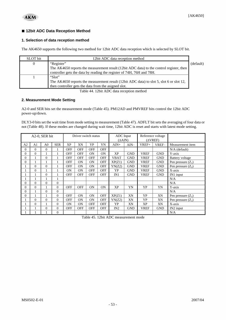
■ 12bit ADC Data Reception Method 1. Selection of data reception method The AK4650 supports the following two method for 12bit ADC data reception which is selected by SLOT bit.
SLOT bit 12bit ADC data reception method 0 “Register”
The AK4650 reports the measurement result (12bit ADC data) to the control register, then controller gets the data by reading the register of 74H, 76H and 78H.
(default)
1 “Slot” The AK4650 reports the measurement result (12bit ADC data) to slot 5, slot 6 or slot 12, then controller gets the data from the asigned slot.
Table 44. 12bit ADC data reception method 2. Measurement Mode Setting A2-0 and SER bits set the measurement mode (Table 45). PM12AD and PMVREF bits control the 12bit ADC power-up/down. DLY3-0 bits set the wait time from mode setting to measurement (Table 47). ADFLT bit sets the averaging of four data or not (Table 48). If these modes are changed during wait time, 12bit ADC is reset and starts with latest mode setting.
A2-0, SER bit Driver switch status ADC Input (ΔAIN)
Reference voltage (ΔVREF)
A2 A1 A0 SER XP XN YP YN AIN+ AIN− VREF+ VREF− Measurement item 0 0 0 1 OFF OFF OFF OFF N/A (default) 0 0 1 1 OFF OFF ON ON XP GND VREF GND Y-axis 0 1 0 1 OFF OFF OFF OFF VBAT GND VREF GND Battery voltage 0 1 1 1 OFF ON ON OFF XP(Z1) GND VREF GND Pen pressure (Z1) 1 0 0 1 OFF ON ON OFF YN(Z2) GND VREF GND Pen pressure (Z2) 1 0 1 1 ON ON OFF OFF YP GND VREF GND X-axis 1 1 0 1 OFF OFF OFF OFF IN1 GND VREF GND IN1 input 1 1 1 1 N/A 0 0 0 0 N/A 0 0 1 0 OFF OFF ON ON XP YN YP YN Y-axis 0 1 0 0 N/A 0 1 1 0 OFF ON ON OFF XP(Z1) XN YP XN Pen pressure (Z1) 1 0 0 0 OFF ON ON OFF YN(Z2) XN YP XN Pen pressure (Z2) 1 0 1 0 ON ON OFF OFF YP XN XP XN X-axis 1 1 0 0 OFF OFF OFF OFF IN2 GND VREF GND IN2 input 1 1 1 0 N/A
Table 45. 12bit ADC measurement mode
[AK4650]
MS0502-E-01 2007/04 - 54 -
PM12AD PMVREF PINTE INTN VREF Function 0 x 0 Disable x 12bit ADC is powered down. Touch screen driver switch is
open. 0 x 1 Enable x The AK4650 waits for pen touch. 12bit ADC is powered down.
Touch screen driver switch is open (though XP pin is TSVDD and YN pin is TSVSS).
1 x 0 Disable x 12bit ADC is always powered up. 1 x 1 Auto x After the measurement of XY or XYZ, 12bit ADC is
automatically powered down and the AK4650 waits for pen touch.
x 0 x x OFF PMVREF bit controls the VREF power-up/down. x 1 x x ON
Table 46. 12bit ADC Power-up/down control (x: Don’t care)
DLY3-0 bit Wait time 0H 1TS (default) 1H 2TS 2H 4TS 3H 8TS 4H 12TS 5H 16TS 6H 24TS 7H 32TS 8H 48TS 9H 64TS AH 96TS BH 128TS CH 160TS DH 192TS EH 224TS FH 256TS
Table 47. Wait time from mode setting to measurement (1TS = 1SYNC period = 20.83μs@fs=48kHz)
ADFLT bit Filter 0 Data is not averaged. The AK4650
outputs one measurement result. (default)
1 Four data are averaged. Table 48. 12bit ADC data filtering (SLOT bit = “0”)
[AK4650]
MS0502-E-01 2007/04 - 55 -
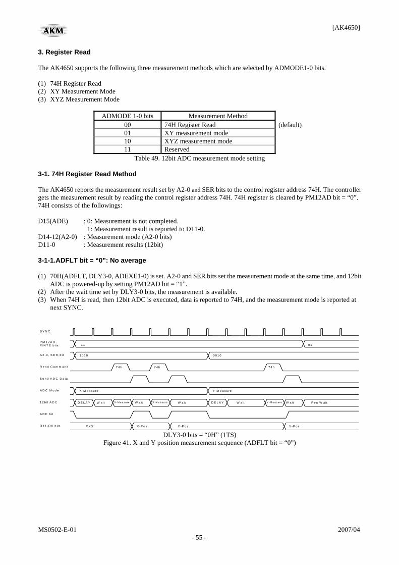
3. Register Read The AK4650 supports the following three measurement methods which are selected by ADMODE1-0 bits. (1) 74H Register Read (2) XY Measurement Mode (3) XYZ Measurement Mode
ADMODE 1-0 bits Measurement Method 00 74H Register Read (default) 01 XY measurement mode 10 XYZ measurement mode 11 Reserved
Table 49. 12bit ADC measurement mode setting 3-1. 74H Register Read Method The AK4650 reports the measurement result set by A2-0 and SER bits to the control register address 74H. The controller gets the measurement result by reading the control register address 74H. 74H register is cleared by PM12AD bit = “0”. 74H consists of the followings: D15(ADE) : 0: Measurement is not completed.
1: Measurement result is reported to D11-0. D14-12(A2-0) : Measurement mode (A2-0 bits) D11-0 : Measurement results (12bit) 3-1-1.ADFLT bit = “0”: No average (1) 70H(ADFLT, DLY3-0, ADEXE1-0) is set. A2-0 and SER bits set the measurement mode at the same time, and 12bit
ADC is powered-up by setting PM12AD bit = “1”. (2) After the wait time set by DLY3-0 bits, the measurement is available. (3) When 74H is read, then 12bit ADC is executed, data is reported to 74H, and the measurement mode is reported at
next SYNC.
S Y N C
A 2 -0 , S E R ,b it
R e a d C o m m a n d
S e n d A D C D a ta
A D C M o d e
A D E b it
1 2 b it A D C
1 0 1 0
X M e a s u re
D E L A Y
D 1 1 -D 0 b its
W a it
X X X X -P o s
7 4 h
X -P o s
0 0 1 0
D E L A Y W a it
P M 1 2 A D , P IN T E b its
Y M e a s u re
Y -P o s
7 4 h
X -M e a s u re W a it X -M e a s u re W a it
7 4 h
Y -M e a s u re W a it P e n W a it
1 1 0 1
DLY3-0 bits = “0H” (1TS)
Figure 41. X and Y position measurement sequence (ADFLT bit = “0”)
[AK4650]
MS0502-E-01 2007/04 - 56 -
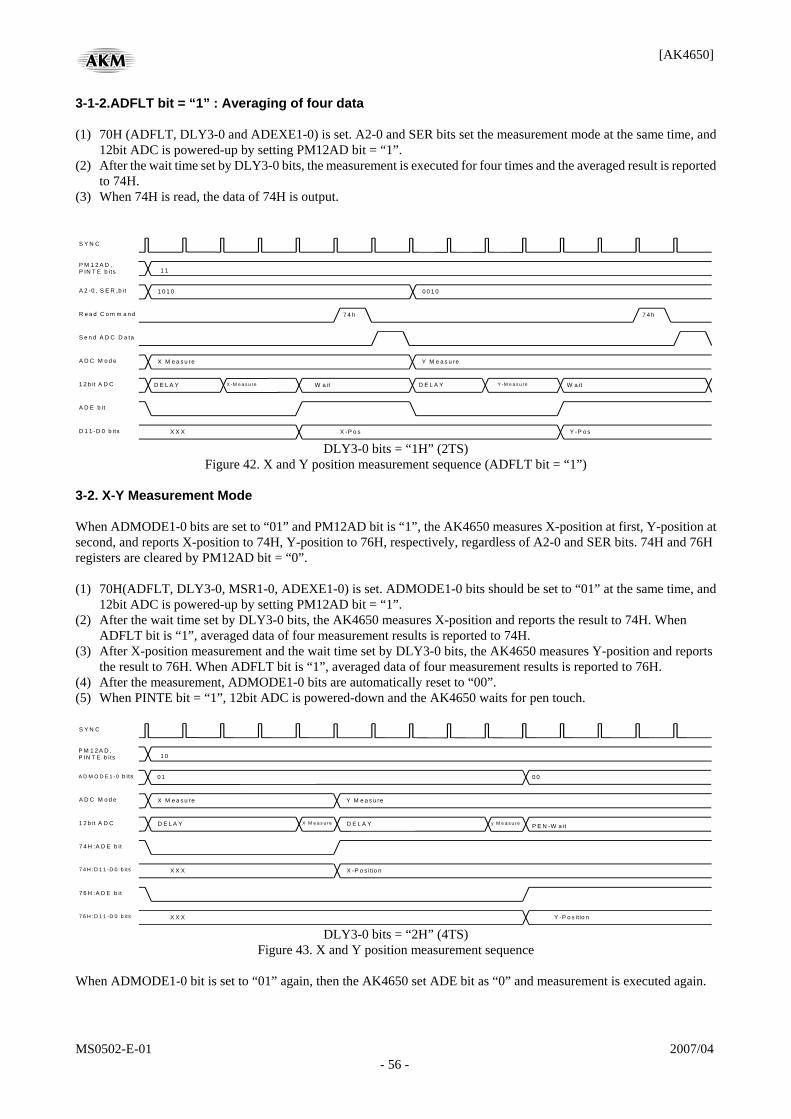
3-1-2.ADFLT bit = “1” : Averaging of four data (1) 70H (ADFLT, DLY3-0 and ADEXE1-0) is set. A2-0 and SER bits set the measurement mode at the same time, and
12bit ADC is powered-up by setting PM12AD bit = “1”. (2) After the wait time set by DLY3-0 bits, the measurement is executed for four times and the averaged result is reported
to 74H. (3) When 74H is read, the data of 74H is output.
S Y N C
A 2 -0 , S E R ,b it
R e a d C o m m a n d
S e n d A D C D a ta
A D C M o d e
A D E b it
1 2 b it A D C
1 0 1 0
X M e a s u re
D E L A Y
D 1 1 -D 0 b its X X X X -P o s
0 0 1 0
D E L A Y
P M 1 2 A D , P IN T E b its
Y M e a s u re
Y -P o s
7 4 h
X -M e a s u re W a it
7 4 h
Y -M e a s u re W a it
1 1
DLY3-0 bits = “1H” (2TS)
Figure 42. X and Y position measurement sequence (ADFLT bit = “1”) 3-2. X-Y Measurement Mode When ADMODE1-0 bits are set to “01” and PM12AD bit is “1”, the AK4650 measures X-position at first, Y-position at second, and reports X-position to 74H, Y-position to 76H, respectively, regardless of A2-0 and SER bits. 74H and 76H registers are cleared by PM12AD bit = “0”. (1) 70H(ADFLT, DLY3-0, MSR1-0, ADEXE1-0) is set. ADMODE1-0 bits should be set to “01” at the same time, and
12bit ADC is powered-up by setting PM12AD bit = “1”. (2) After the wait time set by DLY3-0 bits, the AK4650 measures X-position and reports the result to 74H. When
ADFLT bit is “1”, averaged data of four measurement results is reported to 74H. (3) After X-position measurement and the wait time set by DLY3-0 bits, the AK4650 measures Y-position and reports
the result to 76H. When ADFLT bit is “1”, averaged data of four measurement results is reported to 76H. (4) After the measurement, ADMODE1-0 bits are automatically reset to “00”. (5) When PINTE bit = “1”, 12bit ADC is powered-down and the AK4650 waits for pen touch.
S Y N C
A D C M o d e
7 4 H :A D E b it
1 2 b it A D C
X M e a s u re
D E L A Y
7 4 H :D 1 1 -D 0 b its
X M e a s u re
X X X X -P o s it io n
Y M e a s u re
A D M O D E 1 -0 b its
D E L A Y y M e a s u re
7 6 H :A D E b it
7 6 H :D 1 1 -D 0 b its X X X Y -P o s it io n
0 1
P M 1 2 A D , P IN T E b its 1 0
P E N -W a it
0 0
DLY3-0 bits = “2H” (4TS)
Figure 43. X and Y position measurement sequence When ADMODE1-0 bit is set to “01” again, then the AK4650 set ADE bit as “0” and measurement is executed again.
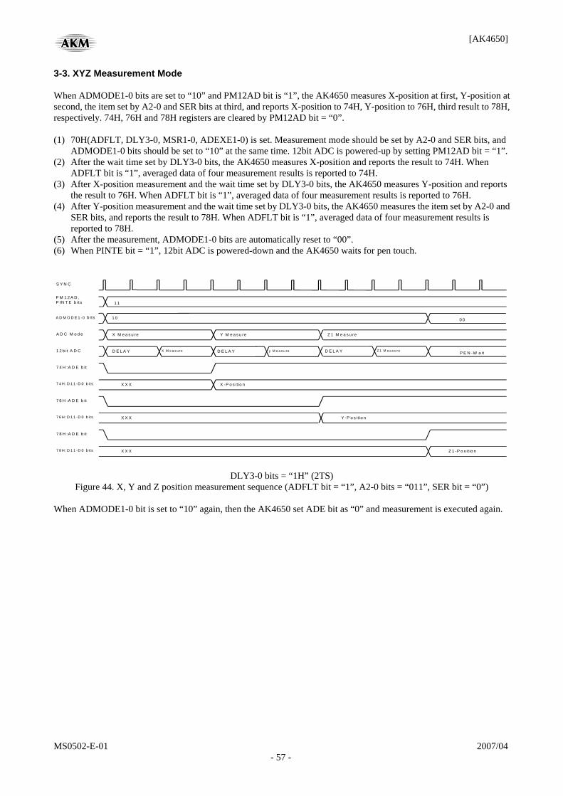
[AK4650]
MS0502-E-01 2007/04 - 57 -
3-3. XYZ Measurement Mode When ADMODE1-0 bits are set to “10” and PM12AD bit is “1”, the AK4650 measures X-position at first, Y-position at second, the item set by A2-0 and SER bits at third, and reports X-position to 74H, Y-position to 76H, third result to 78H, respectively. 74H, 76H and 78H registers are cleared by PM12AD bit = “0”. (1) 70H(ADFLT, DLY3-0, MSR1-0, ADEXE1-0) is set. Measurement mode should be set by A2-0 and SER bits, and
ADMODE1-0 bits should be set to “10” at the same time. 12bit ADC is powered-up by setting PM12AD bit = “1”. (2) After the wait time set by DLY3-0 bits, the AK4650 measures X-position and reports the result to 74H. When
ADFLT bit is “1”, averaged data of four measurement results is reported to 74H. (3) After X-position measurement and the wait time set by DLY3-0 bits, the AK4650 measures Y-position and reports
the result to 76H. When ADFLT bit is “1”, averaged data of four measurement results is reported to 76H. (4) After Y-position measurement and the wait time set by DLY3-0 bits, the AK4650 measures the item set by A2-0 and
SER bits, and reports the result to 78H. When ADFLT bit is “1”, averaged data of four measurement results is reported to 78H.
(5) After the measurement, ADMODE1-0 bits are automatically reset to “00”. (6) When PINTE bit = “1”, 12bit ADC is powered-down and the AK4650 waits for pen touch.
S Y N C
A D C M o d e
7 4 H :A D E b it
1 2 b it A D C
X M e a s u re
D E L A Y
7 4 H :D 1 1 -D 0 b its
X M e a s u re
X X X X -P o s it io n
Y M e a s u re
A D M O D E 1 -0 b its
D E L A Y y M e a s u re
7 6 H :A D E b it
7 6 H :D 1 1 -D 0 b its X X X Y -P o s it io n
1 0
P M 1 2 A D , P IN T E b its 1 1
P E N -W a itD E L A Y Z 1 M e a s u re
7 8 H :A D E b it
7 8 H :D 1 1 -D 0 b its X X X Z 1 -P o s it io n
Z 1 M e a s u re
0 0
DLY3-0 bits = “1H” (2TS) Figure 44. X, Y and Z position measurement sequence (ADFLT bit = “1”, A2-0 bits = “011”, SER bit = “0”)
When ADMODE1-0 bit is set to “10” again, then the AK4650 set ADE bit as “0” and measurement is executed again.
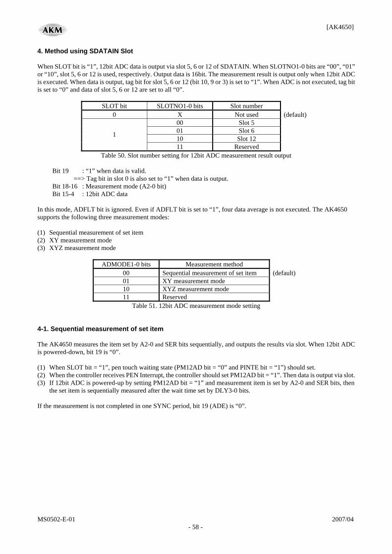
[AK4650]
MS0502-E-01 2007/04 - 58 -
4. Method using SDATAIN Slot When SLOT bit is “1”, 12bit ADC data is output via slot 5, 6 or 12 of SDATAIN. When SLOTNO1-0 bits are “00”, “01” or “10”, slot 5, 6 or 12 is used, respectively. Output data is 16bit. The measurement result is output only when 12bit ADC is executed. When data is output, tag bit for slot 5, 6 or 12 (bit 10, 9 or 3) is set to “1”. When ADC is not executed, tag bit is set to “0” and data of slot 5, 6 or 12 are set to all “0”.
SLOT bit SLOTNO1-0 bits Slot number 0 X Not used (default)
00 Slot 5 01 Slot 6 10 Slot 12 1
11 Reserved Table 50. Slot number setting for 12bit ADC measurement result output
Bit 19 : “1” when data is valid.
==> Tag bit in slot 0 is also set to “1” when data is output. Bit 18-16 : Measurement mode (A2-0 bit) Bit 15-4 : 12bit ADC data
In this mode, ADFLT bit is ignored. Even if ADFLT bit is set to “1”, four data average is not executed. The AK4650 supports the following three measurement modes: (1) Sequential measurement of set item (2) XY measurement mode (3) XYZ measurement mode
ADMODE1-0 bits Measurement method 00 Sequential measurement of set item (default) 01 XY measurement mode 10 XYZ measurement mode 11 Reserved
Table 51. 12bit ADC measurement mode setting 4-1. Sequential measurement of set item The AK4650 measures the item set by A2-0 and SER bits sequentially, and outputs the results via slot. When 12bit ADC is powered-down, bit 19 is “0”. (1) When SLOT bit = “1”, pen touch waiting state (PM12AD bit = “0” and PINTE bit = “1”) should set. (2) When the controller receives PEN Interrupt, the controller should set PM12AD bit = “1”. Then data is output via slot. (3) If 12bit ADC is powered-up by setting PM12AD bit = “1” and measurement item is set by A2-0 and SER bits, then
the set item is sequentially measured after the wait time set by DLY3-0 bits. If the measurement is not completed in one SYNC period, bit 19 (ADE) is “0”.
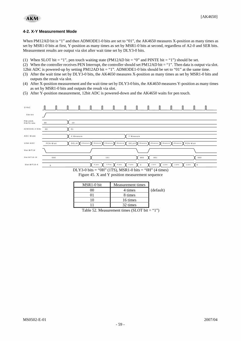
[AK4650]
MS0502-E-01 2007/04 - 59 -
4-2. X-Y Measurement Mode When PM12AD bit is “1” and then ADMODE1-0 bits are set to “01”, the AK4650 measures X-position as many times as set by MSR1-0 bits at first, Y-position as many times as set by MSR1-0 bits at second, regardless of A2-0 and SER bits. Measurement results are output via slot after wait time set by DLY3-0 bits. (1) When SLOT bit = “1”, pen touch waiting state (PM12AD bit = “0” and PINTE bit = “1”) should be set. (2) When the controller receives PEN Interrupt, the controller should set PM12AD bit = “1”. Then data is output via slot. 12bit ADC is powered-up by setting PM12AD bit = “1”. ADMODE1-0 bits should be set to “01” at the same time. (3) After the wait time set by DLY3-0 bits, the AK4650 measures X-position as many times as set by MSR1-0 bits and
outputs the result via slot. (4) After X-position measurement and the wait time set by DLY3-0 bits, the AK4650 measures Y-position as many times
as set by MSR1-0 bits and outputs the result via slot. (5) After Y-position measurement, 12bit ADC is powered-down and the AK4650 waits for pen touch.
S Y N C
A D C M o d e
S lo t B IT 1 9
1 2 b it A D C
X M e a s u re
D E L A Y
S lo t B IT 1 8 -1 6
X M e a s u re
0 0 0 1 0 1
Y M e a s u re
A D M O D E 1 -0 b its
D E L A Y y M e a s u re
0 1
P M 1 2 A D , P IN T E b its 1 0
P E N -W a it
0 0
0 0
S lo t b it
X M e a s u re X M e a s u re X M e a s u re y M e a s u re y M e a s u re y M e a s u re
0 0 0 0 0 1 0 0 0
S lo t B IT 1 5 -4 0 X p o s 0 y p o s 0 X p o s X P o s X p o s y p o s y p o s y p o s
P E N -W a it
DLY3-0 bits = “0H” (1TS), MSR1-0 bits = “0H” (4 times)
Figure 45. X and Y position measurement sequence
MSR1-0 bit Measurement times 00 4 times (default)01 8 times 10 16 times 11 32 times
Table 52. Measurement times (SLOT bit = “1”)
[AK4650]
MS0502-E-01 2007/04 - 60 -
4-3. X-Y-Z Measurement Mode When PM12AD bit is “1” and then ADMODE1-0 bits are set to “10”, the AK4650 measures X-position as many times as set by MSR1-0 bits at first, Y-position as many times as set by MSR1-0 bits at second, the item set by A2-0 and SER bits for times set by MSR1-0 bits at third. Measurement results are output via slot after wait time set by DLY3-0 bits. (1) When SLOT bit = “1”, pen touch waiting state (PM12AD bit = “1” and PINTE bit = “1”) should be set. (2) When the controller receives PEN Interrupt, the controller should set PM12AD bit = “1” so that 12bit ADC is
powered-up. ADMODE1-0 bits should be set to “10” at the same time. Then data is output via slot. (3) After the wait time set by DLY3-0 bits, the AK4650 measures X-position as many times asset by MSR1-0 bits and
outputs the result via slot. (4) After X-position measurement and the wait time set by DLY3-0 bits, the AK4650 measures Y-position as many times
as set by MSR1-0 bits and outputs the result via slot. (5) After Y-position measurement and the wait time set by DLY3-0 bits, the AK4650 measures the item set by A2-0 and
SER bits as many times as set by MSR1-0 bits and outputs the result via slot. (6) After the measurement, 12bit ADC is powered-down and the AK4650 waits for pen touch. 5. ADEXE pin When the AK4650 measures the position during the data is sent to LCD, the position measurement result may have some error caused by the noise from LCD. The AK4650 prepares the measurement mode by using sync signal from LCD after data transferring is completed. The sync signal is input to ADEXE pin of the AK4650.
ADEXE1-0 bit Measurement mode 00 ADC is executed regardless of ADEXE pin. (default)01 ADC is executed at ADEXE pin = “↑”. 10 ADC is executed at ADEXE pin = “↓”. 11 Reserved
Table 53. ADEXE mode ■ Method using Slot 12 of SDATAIN When SLOT bit is “1”, pen interrupt and headphone jack detection results are output via slot 12 of SDATAIN.
Bit 1: Headphone jack detection result Bit 0: Pen interrupt
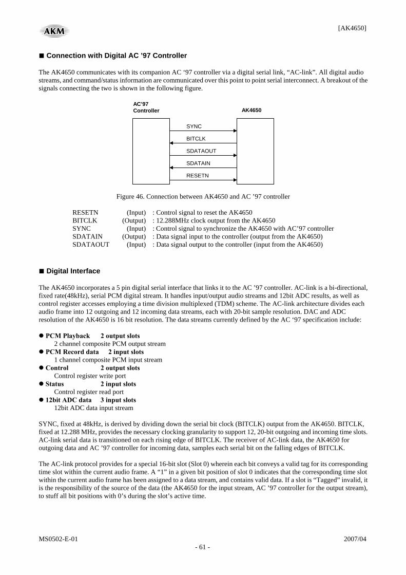
[AK4650]
MS0502-E-01 2007/04 - 61 -
■ Connection with Digital AC ’97 Controller The AK4650 communicates with its companion AC ‘97 controller via a digital serial link, “AC-link”. All digital audio streams, and command/status information are communicated over this point to point serial interconnect. A breakout of the signals connecting the two is shown in the following figure.
SYNC
AC’97 Controller AK4650
BITCLK
SDATAOUT
SDATAIN
RESETN
Figure 46. Connection between AK4650 and AC ’97 controller
RESETN (Input) : Control signal to reset the AK4650 BITCLK (Output) : 12.288MHz clock output from the AK4650 SYNC (Input) : Control signal to synchronize the AK4650 with AC’97 controller SDATAIN (Output) : Data signal input to the controller (output from the AK4650) SDATAOUT (Input) : Data signal output to the controller (input from the AK4650)
■ Digital Interface The AK4650 incorporates a 5 pin digital serial interface that links it to the AC ’97 controller. AC-link is a bi-directional, fixed rate(48kHz), serial PCM digital stream. It handles input/output audio streams and 12bit ADC results, as well as control register accesses employing a time division multiplexed (TDM) scheme. The AC-link architecture divides each audio frame into 12 outgoing and 12 incoming data streams, each with 20-bit sample resolution. DAC and ADC resolution of the AK4650 is 16 bit resolution. The data streams currently defined by the AC ‘97 specification include:
PCM Playback 2 output slots 2 channel composite PCM output stream
PCM Record data 2 input slots 1 channel composite PCM input stream
Control 2 output slots Control register write port
Status 2 input slots Control register read port
12bit ADC data 3 input slots 12bit ADC data input stream
SYNC, fixed at 48kHz, is derived by dividing down the serial bit clock (BITCLK) output from the AK4650. BITCLK, fixed at 12.288 MHz, provides the necessary clocking granularity to support 12, 20-bit outgoing and incoming time slots. AC-link serial data is transitioned on each rising edge of BITCLK. The receiver of AC-link data, the AK4650 for outgoing data and AC ’97 controller for incoming data, samples each serial bit on the falling edges of BITCLK. The AC-link protocol provides for a special 16-bit slot (Slot 0) wherein each bit conveys a valid tag for its corresponding time slot within the current audio frame. A “1” in a given bit position of slot 0 indicates that the corresponding time slot within the current audio frame has been assigned to a data stream, and contains valid data. If a slot is “Tagged” invalid, it is the responsibility of the source of the data (the AK4650 for the input stream, AC ’97 controller for the output stream), to stuff all bit positions with 0’s during the slot’s active time.
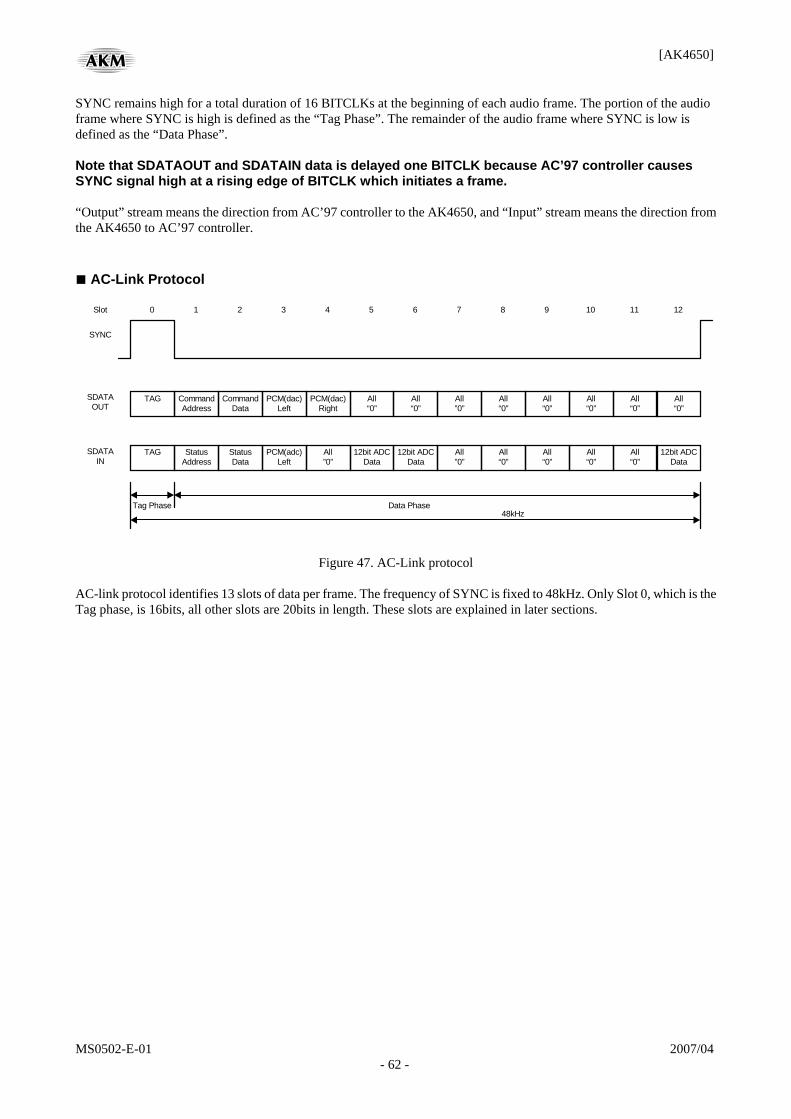
[AK4650]
MS0502-E-01 2007/04 - 62 -
SYNC remains high for a total duration of 16 BITCLKs at the beginning of each audio frame. The portion of the audio frame where SYNC is high is defined as the “Tag Phase”. The remainder of the audio frame where SYNC is low is defined as the “Data Phase”. Note that SDATAOUT and SDATAIN data is delayed one BITCLK because AC’97 controller causes SYNC signal high at a rising edge of BITCLK which initiates a frame. “Output” stream means the direction from AC’97 controller to the AK4650, and “Input” stream means the direction from the AK4650 to AC’97 controller. ■ AC-Link Protocol 12 11 10 9 8 7 6 5 4 3 2 1
48kHz Data Phase Tag Phase
Slot 0
SYNC
All “0”
All “0”
All “0”
All “0”
All ”0”
All “0”
All “0”
PCM(dac)Right
PCM(dac) Left
Command Data
Command Address
TAG
All “0”
All “0”
All “0”
All “0”
All “0”
All ”0”
12bit ADCData
12bit ADCData
All ”0”
PCM(adc) Left
Status Data
Status Address
SDATA IN
TAG
12bit ADCData
SDATA OUT
Figure 47. AC-Link protocol AC-link protocol identifies 13 slots of data per frame. The frequency of SYNC is fixed to 48kHz. Only Slot 0, which is the Tag phase, is 16bits, all other slots are 20bits in length. These slots are explained in later sections.
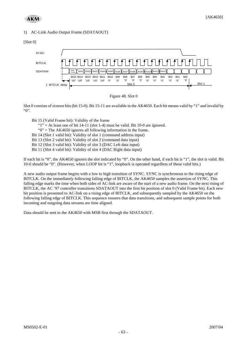
[AK4650]
MS0502-E-01 2007/04 - 63 -
1) AC-Link Audio Output Frame (SDATAOUT) [Slot 0]
“0” Bit5
“1/0” “1/0”
Slot6 Slot7Slot5Slot4Slot3 Slot2 Slot1 Valid Frame
“1/0”
SYNC
Slot 1Slot 0
SDATAIN
BITCLK
“1/0” “1/0” “0”“0” “0”
Slot11
“0” “0” “0” “0” Bit15 Bit14 Bit13 Bit12 Bit11 Bit10 Bit9 Bit8 Bit4 Bit3 Bit2 Bit1
Slot8 Slot10
“0”Bit7
Slot9 Slot12
“0”Bit6
“0” Bit0
1 BITCLK delay
Figure 48. Slot 0
Slot 0 consists of sixteen bits (bit 15-0). Bit 15-11 are available in the AK4650. Each bit means valid by “1” and invalid by “0”.
Bit 15 (Valid Frame bit): Validity of the frame “1” = At least one of bit 14-11 (slot 1-4) must be valid. Bit 10-0 are ignored. “0” = The AK4650 ignores all following information in the frame.
Bit 14 (Slot 1 valid bit): Validity of slot 1 (command address input) Bit 13 (Slot 2 valid bit): Validity of slot 2 (command data input) Bit 12 (Slot 3 valid bit): Validity of slot 3 (DAC Left data input) Bit 11 (Slot 4 valid bit): Validity of slot 4 (DAC Right data input)
If each bit is “0”, the AK4650 ignores the slot indicated by “0”. On the other hand, if each bit is “1”, the slot is valid. Bit 10-0 should be “0”. (However, when LOOP bit is “1”, loopback is operated regardless of these valid bits.) A new audio output frame begins with a low to high transition of SYNC. SYNC is synchronous to the rising edge of BITCLK. On the immediately following falling edge of BITCLK, the AK4650 samples the assertion of SYNC. This falling edge marks the time when both sides of AC-link are aware of the start of a new audio frame. On the next rising of BITCLK, the AC ’97 controller transitions SDATAOUT into the first bit position of slot 0 (Valid Frame bit). Each new bit position is presented to AC-link on a rising edge of BITCLK, and subsequently sampled by the AK4650 on the following falling edge of BITCLK. This sequence ensures that data transitions, and subsequent sample points for both incoming and outgoing data streams are time aligned. Data should be sent to the AK4650 with MSB first through the SDATAOUT.
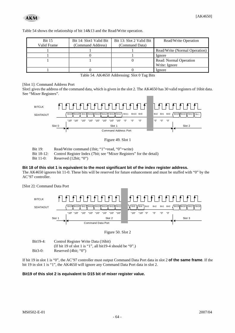
[AK4650]
MS0502-E-01 2007/04 - 64 -
Table 54 shows the relationship of bit 14&13 and the Read/Write operation.
Bit 15 Valid Frame
Bit 14: Slot1 Valid Bit(Command Address)
Bit 13: Slot 2 Valid Bit(Command Data)
Read/Write Operation
1 1 1 Read/Write (Normal Operation)1 0 1 Ignore 1 1 0 Read: Normal Operation
Write: Ignore 1 0 0 Ignore
Table 54. AK4650 Addressing: Slot 0 Tag Bits [Slot 1]: Command Address Port Slot1 gives the address of the command data, which is given in the slot 2. The AK4650 has 30 valid registers of 16bit data. See “Mixer Registers”.
Bit15
“1/0” “1/0”
Bit14Bit16 Bit17 Bit18 Bit19
“1/0”
Command Address Port
Slot 2 Slot 0 Slot 1
SDATAOUT
BITCLK
“1/0” “1/0” “0” “0” “0”
Bit9Bit10Bit12 Bit11Bit13
“1/0” “1/0” “1/0” “0”
Bit2
“0” “0”
Bit16
Bit0 Bit1 Bit17 Bit18 Bit19
Figure 49. Slot 1
Bit 19: Read/Write command (1bit; “1”=read, “0”=write) Bit 18-12: Control Register Index (7bit; see “Mixer Registers” for the detail) Bit 11-0: Reserved (12bit; “0”)
Bit 18 of this slot 1 is equivalent to the most significant bit of the index register address. The AK4650 ignores bit 11-0. These bits will be reserved for future enhancement and must be stuffed with “0” by the AC’97 controller. [Slot 2]: Command Data Port
Bit12Bit15
“1/0” “1/0”
Bit14Bit16 Bit17 Bit18 Bit19
“1/0”
Command Data Port
Slot 3 Slot 1 Slot 2
SDATAOUT
BITCLK
“1/0” “1/0” “0”
Bit3Bit4Bit5Bit6Bit13
“1/0” “1/0” “1/0”“1/0”“1/0” “0”
Bit2
“0” “0”
Bit16Bit0 Bit1 Bit17 Bit18 Bit19
Figure 50. Slot 2
Bit19-4: Control Register Write Data (16bit) (If bit 19 of slot 1 is “1”, all bit19-4 should be “0”.)
Bit3-0: Reserved (4bit; “0”) If bit 19 in slot 1 is “0”, the AC’97 controller must output Command Data Port data in slot 2 of the same frame. If the bit 19 in slot 1 is “1”, the AK4650 will ignore any Command Data Port data in slot 2. Bit19 of this slot 2 is equivalent to D15 bit of mixer register value.

[AK4650]
MS0502-E-01 2007/04 - 65 -
[Slot 3]: PCM Playback Left Channel (16bit) The AK4650 uses the playback (DAC) data format in slot 3 for left channel. Playback data format is MSB first. Data format is 16bits 2’s complement. AC’97 controller should stuff bit 3-0 with “0”. If valid bit (slot 3) in the slot 0 is invalid (“0”), the AK4650 interprets all the data as “0”.
Bit 19-4: Playback data (16bit) Bit 3-0: “0” (4bit)
[Slot 4]: PCM Playback Right Channel (16bit) The AK4650 uses the playback (DAC) data format in slot 4 for right channel. Playback data format is MSB first. Data format is 16bits 2’s complement. AC’97 controller should stuff bit 3-0 with “0”. If valid bit (slot 4) in the slot 0 is invalid (“0”), the AK4650 interprets all the data as “0”.
Bit 19-4: Playback data (16bit) Bit 3-0: “0” (4bit)
[Slot 5-12]: Not implemented in the AK4650
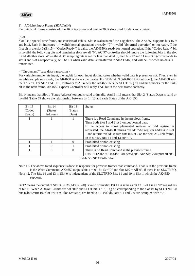
[AK4650]
MS0502-E-01 2007/04 - 66 -
2) AC-Link Input Frame (SDATAIN) Each AC-link frame consists of one 16bit tag phase and twelve 20bit slots used for data and control. [Slot 0] Slot 0 is a special time frame, and consists of 16bits. Slot 0 is also named the Tag phase. The AK4650 supports bits 15-9 and bit 3. Each bit indicates “1”=valid (normal operation) or ready, “0”=invalid (abnormal operation) or not ready. If the first bit in the slot 0 (Bit15 = “Codec Ready”) is valid, the AK4650 is ready for normal operation. If the “Codec Ready” bit is invalid, the following bits and remaining slots are all “0”. AC’97 controller should ignore the following bits in the slot 0 and all other slots. When the ADC sampling rate is set for less than 48kHz, then bits 12 and 11 in slot 0 (corresponds to slot 3 and slot 4 respectively) will be 1’s when valid data is transferred in SDATAIN, and will be 0’s when no data is transmitted. < “On-demand” base data transaction> For variable sample rate input, the tag bit for each input slot indicates whether valid data is present or not. Thus, even in variable sample rate mode, the AK4650 is always the master. For SDATAIN (AK4650 to Controller), the AK4650 sets the TAG bit. For SDATAOUT (Controller to AK4650), the AK4650 sets the SLOTREQ bit and then checks for the TAG bit in the next frame. AK4650 expects Controller will reply TAG bit in the next frame correctly. Bit 14 means that Slot 1 (Status Address) output is valid or invalid. And Bit 13 means that Slot 2 (Status Data) is valid or invalid. Table 55 shows the relationship between bit 14,13 and each Status of the AK4650.
Bit 15 (Codec Ready)
Bit 14 (Status
Address)
Bit 13 (Status Data)
Status
1 1 1 There is a Read Command in the previous frame. Then both Slot 1 and Slot 2 output normal data. If the access to non-implemented register or odd register is requested, the AK4650 returns “valid” 7-bit register address in slot 1 and returns “valid” 0000h data in slot 2 on the next AC-link frame. In this case, Bits 14 and 13 are “1”.
1 1 0 Prohibited or non-existing 1 0 1 Prohibited or non-existing 1 0 0 There is no Read Command in the previous frame.
Bits 19-12 and 9-0 in Slot 1 are set to “0”. And Slot 2 outputs all “0”.Table 55. SDATAIN Slot0
Note 41. The above Read sequence is done as response for previous frames read command. That is, if the previous frame
is the Write Command, AK4650 outputs bit14 =”0”, bit13 =”0” and slot 1&2 = All”0”, if there is no SLOTREQ. Note 42. The Bits 14 and 13 in Slot 0 is independent of the SLOTREQ Bits 11 and 10 in Slot 1 which the AK4650
supports. Bit12 means the output of Slot 3 (PCM(ADC) Left) is valid or invalid. Bit 11 is same as bit 12. Slot 4 is all “0” regardless of bit 11. When ADEXE1-0 bits are not “00” and SLOT bit is “1”, Tag bit corresponding to the slot set by SLOTNO1-0 bits (Slot 5=Bit 10, Slot 6=Bit 9, Slot 12=Bit 3) are fixed to “1” (valid). Bits 8-4 and 2-0 are occupied with “0”.
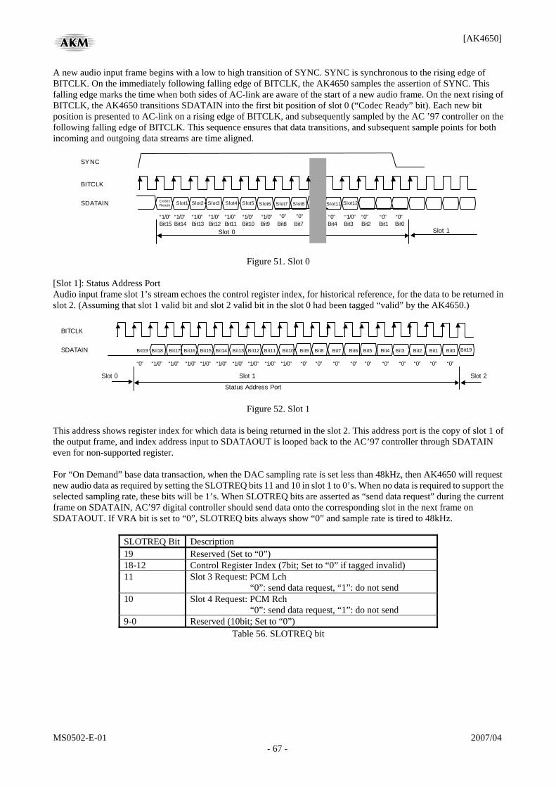
[AK4650]
MS0502-E-01 2007/04 - 67 -
A new audio input frame begins with a low to high transition of SYNC. SYNC is synchronous to the rising edge of BITCLK. On the immediately following falling edge of BITCLK, the AK4650 samples the assertion of SYNC. This falling edge marks the time when both sides of AC-link are aware of the start of a new audio frame. On the next rising of BITCLK, the AK4650 transitions SDATAIN into the first bit position of slot 0 (“Codec Ready” bit). Each new bit position is presented to AC-link on a rising edge of BITCLK, and subsequently sampled by the AC ’97 controller on the following falling edge of BITCLK. This sequence ensures that data transitions, and subsequent sample points for both incoming and outgoing data streams are time aligned.
“0” Bit4
“1/0” “1/0”
Slot6 Slot7Slot5Slot4Slot3 Slot2 Slot1 CodecReady
“1/0”
SYNC
Slot 1 Slot 0
SDATAIN
BITCLK
“1/0” “1/0” “0”“1/0”“1/0”
Slot12
“0” “0” “0” “1/0”Bit15 Bit14 Bit13 Bit12 Bit11 Bit10 Bit9 Bit8 Bit3 Bit2 Bit1 Bit0
Slot8 Slot11
“0”Bit7
Figure 51. Slot 0 [Slot 1]: Status Address Port Audio input frame slot 1’s stream echoes the control register index, for historical reference, for the data to be returned in slot 2. (Assuming that slot 1 valid bit and slot 2 valid bit in the slot 0 had been tagged “valid” by the AK4650.)
Bit15
“1/0” “1/0”
Bit14 Bit16 Bit17 Bit18 Bit19
Status Address Port
Slot 2Slot 0 Slot 1
SDATAIN
BITCLK
“1/0” “1/0” “0”“0”“1/0”“0” “1/0”
Bit8Bit9Bit10Bit12 Bit11Bit13
“1/0” “1/0” “1/0” “0”
Bit7
“0”“0”
Bit1 Bit5Bit6 Bit2 Bit3 Bit4 Bit0 Bit19
“0” “0” “0” “0” “0”
Figure 52. Slot 1 This address shows register index for which data is being returned in the slot 2. This address port is the copy of slot 1 of the output frame, and index address input to SDATAOUT is looped back to the AC’97 controller through SDATAIN even for non-supported register. For “On Demand” base data transaction, when the DAC sampling rate is set less than 48kHz, then AK4650 will request new audio data as required by setting the SLOTREQ bits 11 and 10 in slot 1 to 0’s. When no data is required to support the selected sampling rate, these bits will be 1’s. When SLOTREQ bits are asserted as “send data request” during the current frame on SDATAIN, AC’97 digital controller should send data onto the corresponding slot in the next frame on SDATAOUT. If VRA bit is set to “0”, SLOTREQ bits always show “0” and sample rate is tired to 48kHz.
SLOTREQ Bit Description 19 Reserved (Set to “0”) 18-12 Control Register Index (7bit; Set to “0” if tagged invalid) 11 Slot 3 Request: PCM Lch
“0”: send data request, “1”: do not send 10 Slot 4 Request: PCM Rch
“0”: send data request, “1”: do not send 9-0 Reserved (10bit; Set to “0”)
Table 56. SLOTREQ bit
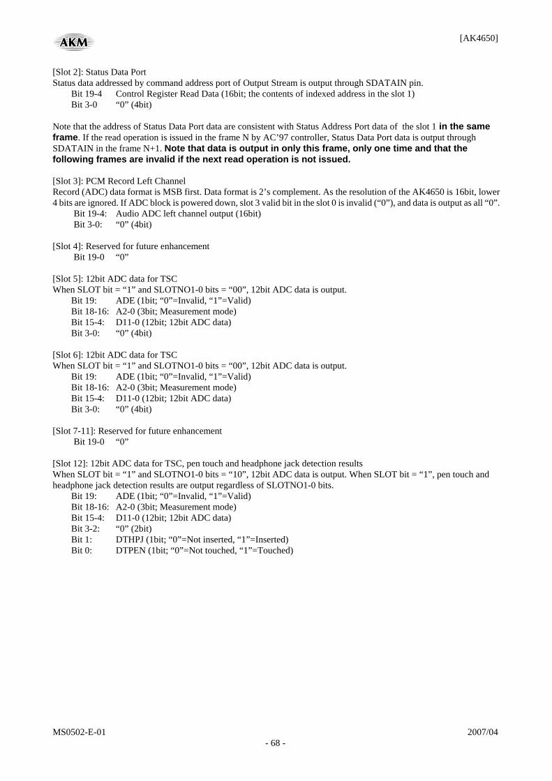
[AK4650]
MS0502-E-01 2007/04 - 68 -
[Slot 2]: Status Data Port Status data addressed by command address port of Output Stream is output through SDATAIN pin.
Bit 19-4 Control Register Read Data (16bit; the contents of indexed address in the slot 1) Bit 3-0 “0” (4bit)
Note that the address of Status Data Port data are consistent with Status Address Port data of the slot 1 in the same frame. If the read operation is issued in the frame N by AC’97 controller, Status Data Port data is output through SDATAIN in the frame N+1. Note that data is output in only this frame, only one time and that the following frames are invalid if the next read operation is not issued. [Slot 3]: PCM Record Left Channel Record (ADC) data format is MSB first. Data format is 2’s complement. As the resolution of the AK4650 is 16bit, lower 4 bits are ignored. If ADC block is powered down, slot 3 valid bit in the slot 0 is invalid (“0”), and data is output as all “0”.
Bit 19-4: Audio ADC left channel output (16bit) Bit 3-0: “0” (4bit)
[Slot 4]: Reserved for future enhancement
Bit 19-0 “0” [Slot 5]: 12bit ADC data for TSC When SLOT bit = “1” and SLOTNO1-0 bits = “00”, 12bit ADC data is output.
Bit 19: ADE (1bit; “0”=Invalid, “1”=Valid) Bit 18-16: A2-0 (3bit; Measurement mode) Bit 15-4: D11-0 (12bit; 12bit ADC data) Bit 3-0: “0” (4bit)
[Slot 6]: 12bit ADC data for TSC When SLOT bit = “1” and SLOTNO1-0 bits = “00”, 12bit ADC data is output.
Bit 19: ADE (1bit; “0”=Invalid, “1”=Valid) Bit 18-16: A2-0 (3bit; Measurement mode) Bit 15-4: D11-0 (12bit; 12bit ADC data) Bit 3-0: “0” (4bit)
[Slot 7-11]: Reserved for future enhancement
Bit 19-0 “0” [Slot 12]: 12bit ADC data for TSC, pen touch and headphone jack detection results When SLOT bit = “1” and SLOTNO1-0 bits = “10”, 12bit ADC data is output. When SLOT bit = “1”, pen touch and headphone jack detection results are output regardless of SLOTNO1-0 bits.
Bit 19: ADE (1bit; “0”=Invalid, “1”=Valid) Bit 18-16: A2-0 (3bit; Measurement mode) Bit 15-4: D11-0 (12bit; 12bit ADC data) Bit 3-2: “0” (2bit) Bit 1: DTHPJ (1bit; “0”=Not inserted, “1”=Inserted) Bit 0: DTPEN (1bit; “0”=Not touched, “1”=Touched)
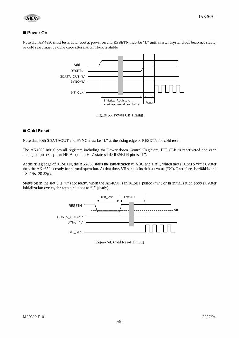
[AK4650]
MS0502-E-01 2007/04 - 69 -
■ Power On Note that AK4650 must be in cold reset at power on and RESETN must be “L” until master crystal clock becomes stable, or cold reset must be done once after master clock is stable.
BIT_CLK
Initialize Registers start up crystal oscillation
SYNC=”L”SDATA_OUT=”L”
RESETN
Vdd
Trst2clk
Figure 53. Power On Timing ■ Cold Reset Note that both SDATAOUT and SYNC must be “L” at the rising edge of RESETN for cold reset. The AK4650 initializes all registers including the Power-down Control Registers, BIT-CLK is reactivated and each analog output except for HP-Amp is in Hi-Z state while RESETN pin is “L”. At the rising edge of RESETN, the AK4650 starts the initialization of ADC and DAC, which takes 1028TS cycles. After that, the AK4650 is ready for normal operation. At that time, VRA bit is its default value (“0”). Therefore, fs=48kHz and TS=1/fs=20.83μs. Status bit in the slot 0 is “0” (not ready) when the AK4650 is in RESET period (“L”) or in initialization process. After initialization cycles, the status bit goes to “1” (ready).
BIT_CLK
VIL RESETN
Trst2clkTrst_low
SYNC= “L”SDATA_OUT= “L”
Figure 54. Cold Reset Timing
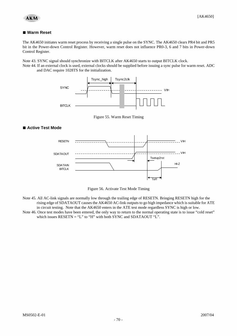
[AK4650]
MS0502-E-01 2007/04 - 70 -
■ Warm Reset The AK4650 initiates warm reset process by receiving a single pulse on the SYNC. The AK4650 clears PR4 bit and PR5 bit in the Power-down Control Register. However, warm reset does not influence PR0-3, 6 and 7 bits in Power-down Control Register. Note 43. SYNC signal should synchronize with BITCLK after AK4650 starts to output BITCLK clock. Note 44. If an external clock is used, external clocks should be supplied before issuing a sync pulse for warm reset. ADC
and DAC require 1028TS for the initialization.
VIH
Tsync2clk Tsync_high
BITCLK
SYNC
Figure 55. Warm Reset Timing ■ Active Test Mode
VIH
VIH
Tsetup2rst
Toff
SDATAIN BITCLK
SDATAOUT
HI-Z
RESETN
Figure 56. Activate Test Mode Timing Note 45. All AC-link signals are normally low through the trailing edge of RESETN. Bringing RESETN high for the
rising edge of SDATAOUT causes the AK4650 AC-link outputs to go high impedance which is suitable for ATE in circuit testing. Note that the AK4650 enters in the ATE test mode regardless SYNC is high or low.
Note 46. Once test modes have been entered, the only way to return to the normal operating state is to issue “cold reset” which issues RESETN = “L” to “H” with both SYNC and SDATAOUT “L”.
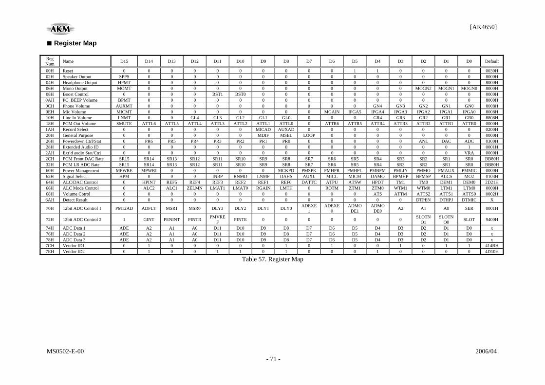
[AK4650]
MS0502-E-00 2006/04 - 71 -
■ Register Map Reg Num Name D15 D14 D13 D12 D11 D10 D9 D8 D7 D6 D5 D4 D3 D2 D1 D0 Default
00H Reset 0 0 0 0 0 0 0 0 0 0 1 1 0 0 0 0 0030H 02H Speaker Output SPPS 0 0 0 0 0 0 0 0 0 0 0 0 0 0 0 8000H 04H Headphone Output HPMT 0 0 0 0 0 0 0 0 0 0 0 0 0 0 0 8000H 06H Mono Output MOMT 0 0 0 0 0 0 0 0 0 0 0 0 MOGN2 MOGN1 MOGN0 8000H 08H Boost Control 0 0 0 0 BST1 BST0 0 0 0 0 0 0 0 0 0 0 0000H 0AH PC_BEEP Volume BPMT 0 0 0 0 0 0 0 0 0 0 0 0 0 0 0 8000H 0CH Phone Volume AUXMT 0 0 0 0 0 0 0 0 0 0 GN4 GN3 GN2 GN1 GN0 8008H 0EH Mic Volume MICMT 0 0 0 0 0 0 0 0 MGAIN IPGA5 IPGA4 IPGA3 IPGA2 IPGA1 IPGA0 8008H 10H Line In Volume LNMT 0 0 GL4 GL3 GL2 GL1 GL0 0 0 0 GR4 GR3 GR2 GR1 GR0 8808H 18H PCM Out Volume SMUTE ATTL6 ATTL5 ATTL4 ATTL3 ATTL2 ATTL1 ATTL0 0 ATTR6 ATTR5 ATTR4 ATTR3 ATTR2 ATTR1 ATTR0 0000H 1AH Record Select 0 0 0 0 0 0 MICAD AUXAD 0 0 0 0 0 0 0 0 0200H 20H General Purpose 0 0 0 0 0 0 MDIF MSEL LOOP 0 0 0 0 0 0 0 0000H 26H Powerdown Ctrl/Stat 0 PR6 PR5 PR4 PR3 PR2 PR1 PR0 0 0 0 0 0 ANL DAC ADC 0300H 28H Extended Audio ID 0 0 0 0 0 0 0 0 0 0 0 0 0 0 0 1 0001H 2AH Ext’d audio Stat/Ctrl 0 0 0 0 0 0 0 0 0 0 0 0 0 0 0 VRA 0000H 2CH PCM Front DAC Rate SR15 SR14 SR13 SR12 SR11 SR10 SR9 SR8 SR7 SR6 SR5 SR4 SR3 SR2 SR1 SR0 BB80H 32H PCM LR ADC Rate SR15 SR14 SR13 SR12 SR11 SR10 SR9 SR8 SR7 SR6 SR5 SR4 SR3 SR2 SR1 SR0 BB80H 60H Power Management MPWRE MPWRI 0 0 0 0 0 MCKPD PMSPK PMHPR PMHPL PMBPM PMLIN PMMO PMAUX PMMIC 0000H 62H Signal Select HPM 0 0 0 INBP RNMD LNMP DAHS AUXL MICL MICM DAMO BPMHP BPMSP ALCS MO2 0103H 64H ALC/DAC Control 0 HPINT REF5 REF4 REF3 REF2 REF1 REF0 DATTC ATPU ATSW HPDT TM1 TM0 DEM1 DEM0 2D21H 66H ALC Mode Control 0 ALC2 ALC1 ZELMN LMAT1 LMAT0 RGAIN LMTH 0 ROTM ZTM1 ZTM0 WTM1 WTM0 LTM1 LTM0 0000H 68H Volume Cotrol 0 0 0 0 0 0 0 0 0 0 0 ATS ATTM ATTS2 ATTS1 ATTS0 0002H 6AH Detect Result 0 0 0 0 0 0 0 0 0 0 0 0 0 DTPEN DTHPJ DTMIC X
70H 12bit ADC Control 1 PM12AD ADFLT MSR1 MSR0 DLY3 DLY2 DLY1 DLY0 ADEXE1
ADEXE0
ADMODE1
ADMODE0 A2 A1 A0 SER 0001H
72H 12bit ADC Control 2 1 GINT PENINT PINTR PMVREF PINTE 0 0 0 0 0 0 0 SLOTN
O1 SLOTN
O0 SLOT 9400H
74H ADC Data 1 ADE A2 A1 A0 D11 D10 D9 D8 D7 D6 D5 D4 D3 D2 D1 D0 x 76H ADC Data 2 ADE A2 A1 A0 D11 D10 D9 D8 D7 D6 D5 D4 D3 D2 D1 D0 x 78H ADC Data 3 ADE A2 A1 A0 D11 D10 D9 D8 D7 D6 D5 D4 D3 D2 D1 D0 x 7CH Vendor ID1 0 1 0 0 0 0 0 1 0 1 0 0 1 0 1 1 414BH 7EH Vendor ID2 0 1 0 0 1 1 0 1 0 0 0 1 0 0 0 0 4D10H
Table 57. Register Map
[AK4650]
MS0502-E-01 2007/04 - 72 -
■ Speaker Output (02H)
SPPS: Speaker-amp Power-Save-Mode (Table 38) 0: Normal Operation 1: Power Save Mode (default) When the SPPS bit = “1”, the Speaker-amp is in power-save-mode and the SPP pin becomes Hi-Z and SPN pin is set to HVDD/2 voltage. When the PMSPK bit = “1”, this bit is valid. After the RESETN pin changes from “L” to “H”, the PMSPK bit is “0”, which powers down Speaker-amp
■ Headphone Output (04H)
HPMT: Headphone Amp Mute Control (Figure 26) 0: Mute OFF 1: Mute ON (default)
■ Mono Output (06H)
MOMT: Mono Output Mute Control (Table 30) 0: Mute OFF 1: Mute ON (default)
MOGN2-0: MOUT Volume Control (Table 31)
Default: “000” (+6dB) ■ Boost Control (08H)
BST1-0: Bass Boost Control (Table 24) Default: “00” (OFF)
■ BEEP Volume (0AH)
BPMT: BEEP Input Mute Control 0: Mute OFF 1: Mute ON (default)
■ Phone Volume (0CH)
AUXMT: AUX Input Mute Control (Table 28) 0: Mute OFF 1: Mute ON (default)
GN4-0: AUX Input Volume Control (Table 28)
Default: “08H” (0dB) ■ MIC Volume (0EH)
MICMT: Mic Input Mute Control (Table 14) 0: Mute OFF 1: Mute ON (default)
MGAIN: MIC-Amp Gain Control (Table 10)
0: 0dB (default) 1: +20dB
IPGA5-0: IPGA Control (Table 14)
Default: “08H” (0dB)
[AK4650]
MS0502-E-01 2007/04 - 73 -
■ Line In Volume (10H)
LNMT: Line Input Mute Control (Table 29) 0: Mute OFF 1: Mute ON (default)
GL4-0: Lch Line Input Volume Control (Table 29)
Default: “08H” (0dB)
GR4-0: Rch Line Input Volume Control (Table 29) Default: “08H” (0dB)
■ PCM Volume (18H)
SMUTE: Soft Mute Control (Figure 21) 0: Normal Operation (default) 1: DAC outputs soft-muted
Soft mute operation is independent of digital attenuator and is performed in the digital domain.
ATTL/R6-0: Digital ATT Control (Table 25) Default: “00H”(0dB)
■ Record Select Control Register (1AH)
AUXAD: AUXIN to ADC enable 0: OFF (default) 1: ON
MICAD: IPGA to ADC enable
0: OFF 1: ON (default)
■ General Purpose (20H)
LOOP: Internal Digital Loopback 0: OFF (default) 1: ON When LOOP bit is “1”, VRA bit should be “0”.
MSEL: Internal/External MIC Select (Table 9 at MDIF bit = “0”)
0: Internal MIC (default) 1: External MIC
MDIF: Differential MIC Input Select (Table 9)
0: Single-ended Input (default) 1: Differential Input
[AK4650]
MS0502-E-01 2007/04 - 74 -
■ Power Management (26H)
PR6-0: Power Management (Table 6) Default: “0000011” (ADC, DAC Power down)
REF: Internal VREF Power-up (Read only)
0: NOT Ready 1: Ready
ANL: Analog Mixer Power-up (Read only)
0: NOT Ready 1: Ready
DAC: DAC ready to accept data (Read only)
0: NOT Ready 1: Ready
ADC: ADC ready to transmit data (Read only)
0: NOT Ready 1: Ready
■ Extended Audio Status & Control (2AH)
VRA: Enables Variable Rate Audio mode in conjunction with Audio Sample Rate Control Registers and tag-bit/SLOTREQ signaling.
0: OFF(default). PLL is powered-down. 1: ON
■ Audio Sample Rate control Registers (2CH, 32H)
SR15-0: Sample Rate Control for DAC (2CH) and ADC (32H) (Table 4, Table 5) Default: “BB80H”(48kHz)
These Sample Rate setting is done at VRA bit = “1”.
[AK4650]
MS0502-E-01 2007/04 - 75 -
■ Power Management (60H)
PMMIC: MIC Block (MIC-Amp and ALC1) Power Management 0: Power down (default) 1: Power up
PMAUX: AUX Input Power Management
0: Power down (default) 1: Power up
PMMO: Mono Line Output Power Management
0: Power down (default) 1: Power up
PMLIN: Stereo Line Input Power Management
0: Power down (default) 1: Power up
PMBPM: Mono Beep Input Power Management
0: Power down (default) 1: Power up
Even if PMBPM= “0”, the path is still connected between BEEP pin and HP/SPK-Amp. BPMHP and BPMSP bits should be set to “0” to disconnect these paths, respectively.
PMHPR: Headphone-Amp Rch Power Management
0: Power down (default) 1: Power up
PMHPL: Headphone-Amp Lch Power Management
0: Power down (default) 1: Power up
PMSPK: Speaker-Amp Power Management
0: Power down (default) 1: Power up
MCKPD: XTI pin pull down control
0: Master Clock input enable (default) 1: XTI pin is internally pulled-down
MPWRI: Internal MIC Power Supply Control (Table 11)
0: OFF (default) 1: MIC Power is ON for Internal MIC.
MPWRI bit is enabled when PMMIC bit = “1”.
MPWRE: External MIC Power Supply Control (Table 12) 0: OFF (default) 1: MIC Power is ON for External MIC.
MPWRE bit is enabled when PMMIC bit = “1”.
[AK4650]
MS0502-E-01 2007/04 - 76 -
■ Signal Select (62H)
MO2: Mono Output (MOUT2 pin) Enable 0: OFF 1: ON (default)
When MO2 bit = “0”, MOUT2 pin outputs VCOM voltage. MOUT2 pin outputs signal when MO2 bit = “1” and PMSPK bit = “1”. MOUT2 pin goes to Hi-Z state when PMSPK bit = “0”.
ALCS: ALC2 to Speaker-Amp Enable
0: OFF 1: ON (default)
BPMSP: BEEP to Speaker-Amp Enable
0: OFF (default) 1: ON
BPMHP: BEEP to Headphone-Amp Enable
0: OFF (default) 1: ON
DAMO: DAC to Mono Line Output Enable
0: OFF (default) 1: ON
MICM: IPGA to Mono Line Output Enable
0: OFF (default) 1: ON
MICL: IPGA to Headphone/Speaker-Amp Enable
0: OFF (default) 1: ON
AUXL: AUXIN to Headphone/Speaker-Amp Enable
0: OFF (default) 1: ON
DAHS: DAC to Headphone/Speaker-Amp Enable
0: OFF 1: ON (default)
LNMP: LIN/MPE pin Selection
0: MPE pin (Default) 1: LIN pin
RNMD: RIN/MDT pin Selection
0: MDT pin (default) 1: RIN pin
INBP: IN2/BEEP pin Selection
0: BEEP pin (default) 1: IN2 pin
HPM: Mono Output Select of Headphone
0: Stereo (default) 1: Mono [(L+R)/2]
[AK4650]
MS0502-E-01 2007/04 - 77 -
■ ALC/DAC Control (64H)
DEM1-0: De-emphases response (Table 23) Default: “01” (OFF)
TM1-0: Soft Mute Time Select (Table 27)
Default: “00” (1024/fs)
HPDT: Headphone Jack Insertion Detection Function Enable 0: OFF (default) 1: ON
ATSW: Headphone/Speaker Automatic Switch Function Enable by Headphone Jack Insertion (Table 35, Table 36)
0: OFF 1: ON (default)
ATPU: Headphone-Amp Automatic Power-up Function Enable by Pen Touch (Figure 38)
0: OFF (default) 1: ON
DATTC: DAC Digital Attenuator Control Mode Select
0: Independent 1: Dependent (default)
When DATTC= “1”, ATTL6-0 bits control both Lch and Rch at the same time. ATTR6-0 bits are not changed when the ATTL6-0 bits are written.
REF5-0: Maximum IPGA value at ALC1 Recovery Operation (Table 21)
Default: “2DH” (+19dB) During the ALC1 recovery operation, if the IPGA value exceeds the setting maximum value (REF5-0 bits) by gain operation, then the IPGA does not become larger than the maximum value.
HPINT: INTN pin Output Enable for Headphone Jack Detection
Default: “0” (OFF) When HPINT bit = “1”, INTN pin is enabled to output the interrupt signal of headphone jack detection.
■ ALC Control (66H)
LTM1-0: ALC1 limiter operation period at zero crossing disable (ZELMN bit = “1”) (Table 17) Default: “00” (0.5/fs)
The IPGA value is changed immediately when zero crossing is disabled (ZELMN bit = “1”). When the IPGA value is changed continuously, the change is done by the period specified by the LTM1-0 bits.
WTM1-0: ALC1 Recovery Waiting Period (Table 19)
Default: “00” (128/fs) WTM1-0 bits set a period of recovery operation when any limiter operation does not occur during the ALC1 operation.
ZTM1-0: ALC1 zero crossing timeout selection (Table 18)
Default: “00” (128/fs) When the IPGA performs zero crossing or timeout, the IPGA value is changed by the μP WRITE operation, ALC1 recovery operation or ALC1 limiter operation (ZELMN bit = “0”).
[AK4650]
MS0502-E-01 2007/04 - 78 -
ROTM: ALC2 Recovery Waiting Period (Table 39) 0: 2048/fs (default) 1: 512/fs
LMTH: ALC1 Limiter Detection Level / Recovery Waiting Counter Reset Level (Table 15)
Default: “0” (−6dB/−8dB) The ALC1 limiter detection level and the ALC1 recovery counter reset level may be offset by about ±2dB.
RGAIN: ALC1 Recovery GAIN Step (Table 20)
Default: “0” (0.5dB) During the ALC1 recovery operation, RGAIN bit sets the number of steps changed from the current IPGA value. For example, when the current IPGA value is “30H” and RGAIN bit is “1”, the IPGA changes to “32H” by the ALC1 recovery operation and the output signal level is gained up by 1dB (=0.5dB x 2). When the IPGA value exceeds the maximum level (REF5-0 bits), the IPGA value does not increase.
LMAT1-0: ALC1 Limiter ATT Step (Table 16)
Default: “00” (0.5dB) During the ALC1 limiter operation, when IPGA value exceeds the ALC1 limiter detection level set by LMTH bit, LMAT1-0 bits set the number of steps attenuated from the current IPGA value. For example, when the current IPGA value is “47H” and LMAT1-0 bits is “11”, the IPGA value decreases to “43H” when the ALC1 limiter operation starts, resulting in the input signal level being attenuated by 2dB (=0.5dB x 4). When the attenuation value exceeds IPGA = “00H” (−8dB), it clips to “00H”.
ZELMN: Zero crossing detection enable at ALC1 Limiter operation
0: Enable (default) 1: Disable
When the ZELMN bit = “0”, the IPGA performs a zero crossing or timeout and the IPGA value is changed by the ALC1 operation. The zero crossing timeout is the same as the ALC1 recovery operation. When the ZELMN bit = “1”, the IPGA value is changed immediately.
ALC1: ALC1 enable
0: ALC1 Disable (default) 1: ALC1 Enable
ALC2: ALC2 enable
0: ALC2 Disable (default) 1: ALC2 Enable
■ Volume Control (68H)
ATTS2-0: Volume control of signal from IPGA to Headphone/Speaker-Amp (Table 7) Default: “2H” (−12dB)
ATTM: Volume control of signal from IPGA to Mono Line Output (Table 8) 0: 0dB (default) 1: −4dB
ATS: Digital attenuator transition time setting (Table 26)
Default: “0” (531/fs)

[AK4650]
MS0502-E-01 2007/04 - 79 -
■ Detect Result (6AH)
DTMIC: MIC detection result (Read only, Table 13) 0: Microphone is not detected. 1: Microphone is detected
DTHPJ: Headphone jack insertion detection result (Read only, Table 34)
0: Headphone jack is not inserted. 1: Headphone jack is inserted.
DTPEN: Pen touch detection result when PM12AD bit = “0”, PENINT bit = “1” and PINTR bit = “1” (Read only) 0: Pen is not touched. 1: Pen is touched.
[AK4650]
MS0502-E-01 2007/04 - 80 -
■ 12bit ADC Control 1 (70H)
A2-0, SER: 12bit ADC measurement item select (Table 45) Default: “0001” (N/A)
ADMODE1-0: 12bit ADC measurement mode select (Table 49, Table 51)
Default: “00” (74H Register Read)
ADEXE1-0: ADEXE mode select (Table 53) Default: “00” (Mode 0)
DLY3-0: Wait time select from mode setting to ADC execution (Table 47)
Default: “0000” (1TS)
MSR1-0: Measurement times select (Table 52) Default: “00” (4 times)
ADFLT: 12bit ADC data filtering select (Table 48)
0: OFF (default) 1: 4 data averaging
PM12AD: 12bit ADC for touch screen controller power management (Table 6)
0: Power Down (default) 1: Power Up
[AK4650]
MS0502-E-01 2007/04 - 81 -
■ 12bit ADC Control 2 (72H)
SLOT: 12bit ADC data reception method select (Table 44) 0: Register (default) 1: Slot
SLOTNO1-0: 12bit ADC measurement result output slot select (Table 50)
Default: “00” (Slot 5)
PINTE: 12bit ADC for touch screen controller power management (Table 46) 0: Power Down 1: Power Up (default)
PMVREF: Internal reference voltage for touch screen controller power management (Table 46)
0: Power Down (default) 1: Power Up
PINTR: DTPEN bit output enable for pen interrupt
Default: “1” (ON) When PINTR bit is “1”, pen interrupt is output at DTPEN bit.
PENINT: INTN pin output enable for pen interrupt
Default: “0” (OFF) When PENINT bit is “1”, pen interrupt is output via INTN pin.
GINT: Slot output enable for pen interrupt
Default: “0” (OFF) When GINT bit is “1” and AC-link operates, pen interrupt is output at bit 0 of slot 12 on SDATAIN.
■ 12bit ADC Data (74H, 76H, 78H)
ADE: Measurement data valid (Read only) 0: Invalid 1: Valid
A2-0: Measurement item (Read only, Table 45)
D11-0: 12bit ADC measurement data (Read only)
■ Vendor ID (7CH, 7EH)
“A(41H), K(4BH), M(4DH), 16(10H)” (Read only)
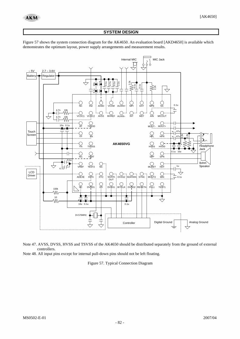
[AK4650]
MS0502-E-01 2007/04 - 82 -
SYSTEM DESIGN Figure 57 shows the system connection diagram for the AK4650. An evaluation board [AKD4650] is available which demonstrates the optimum layout, power supply arrangements and measurement results.
NC IN2 AVDD VCOM AUXIN+ MPI EXT MPE NC
VCOC1 VCOC2 AVSS MVREF AUXIN− INT MDT AIN MICOUT
XP TSVDD MOUT− MOUT+
YP XN HPL HPR
YN TSVSS HVSS HVDD
IN1 VBAT SPP SPN
VREF TEST2 MUTET HDT
ADEXE INTN XTO SDATAOUT
DVSS2 SDATAIN SYNC MOUT2 MIN
NC DVDD1 XTI DVSS1 BITCLK DVDD2 RESETN PLL1 TEST1
NC
AK4650VG
10k 4.7n
10k 4.7n
Touch Screen
Battery Regulator
LCD Driver
0.1u 10u
4.7u
0.1u
0.1u
4.7u
0.1u
2.2u
2.2k
0.1u
0.1u
2.2k
0.1u
10u 0.1u
2.2k
2.2k
0.1u
1u
10
0.1u0.1u 10u
Controller
Internal MIC MIC Jack
HeadphoneJack
8ohm Speaker
0.1u
10
u
24.576MHz
Analog Ground Digital Ground
2.7 ∼ 3.6V ∼ 5V
+
+
+
+
+
100k
47u
47u
+
+
Note 47. AVSS, DVSS, HVSS and TSVSS of the AK4650 should be distributed separately from the ground of external
controllers. Note 48. All input pins except for internal pull-down pins should not be left floating.
Figure 57. Typical Connection Diagram
[AK4650]
MS0502-E-01 2007/04 - 83 -
1. Grounding and Power Supply Decoupling The AK4650 requires careful attention to power supply and grounding arrangements. AVDD, DVDD, HVDD and TSVDD are usually supplied from the system’s analog supply. If AVDD, DVDD, HVDD and TSVDD are supplied separately, the correct power up sequence should be observed. AVSS, DVSS, HVSS and TSVSS of the AK4650 should be connected to the analog ground plane. System analog ground and digital ground should be connected together near to where the supplies are brought onto the printed circuit board. Decoupling capacitors should be as near to the AK4538 as possible, with the small value ceramic capacitor being the nearest. 2. Voltage Reference VCOM is a signal ground of this chip. A 2.2μF electrolytic capacitor in parallel with a 0.1μF ceramic capacitor attached to the VCOM pin eliminates the effects of high frequency noise. No load current may be drawn from the VCOM pin. All signals, especially clocks, should be kept away from the VREF and VCOM pins in order to avoid unwanted coupling into the AK4650. 3. Analog Inputs The Mic, Beep and stereo line inputs are single-ended. AUX input is differential. The input signal range scales with nominally at 0.06 x AVDD Vpp for the Mic input, 0.6 x AVDD Vpp for the Beep input, stereo line input and AUX input, centered around the internal common voltage (0.45 x AVDD). Usually the input signal is AC coupled using a capacitor. The cut-off frequency is fc = 1/(2πRC). The AK4650 can accept input voltages from AVSS to AVDD. 4. Analog Outputs The input data format for the DAC is 2’s complement. The output voltage is a positive full scale for 7FFFH(@16bit) and a negative full scale for 8000H(@16bit). Mono output from the MOUT2 pin and Mono Line Output from the MOUT+/MOUT− pins are centered at 0.45 x AVDD, Headphone-Amp is centered at 0.44 x AVDD and Speaker-Amp output is centered at HVDD/2, respectively.
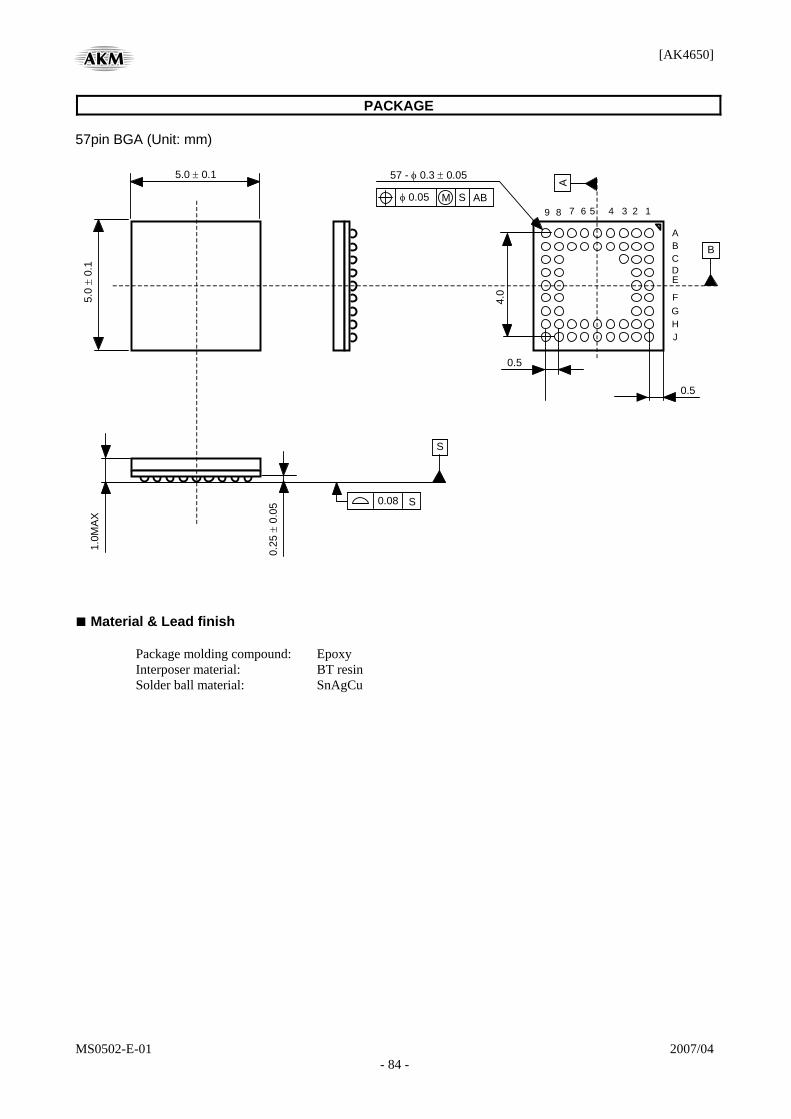
[AK4650]
MS0502-E-01 2007/04 - 84 -
PACKAGE 57pin BGA (Unit: mm)
5.0 ±
0.1
5.0 ± 0.1
0.5
ABCDE
FG
7 6 5 4 3 2 1 57 - φ 0.3 ± 0.05
HJ
9 8
0.08 S
S
φ 0.05 ABS
B
0.5
M
A
4.0
1.0M
AX
0.25
± 0
.05
■ Material & Lead finish Package molding compound: Epoxy Interposer material: BT resin Solder ball material: SnAgCu
[AK4650]
MS0502-E-01 2007/04 - 85 -
MARKING
4650 XXXX
XXXX: Date code (4 digit) Pin #1 indication
REVISION HISTORY Date (YY/MM/DD) Revision Reason Page Contents 06/04/24 00 First Edition 07/04/18 01 Error correct 7 Pin/Function
VCOM pin: “Common Voltage Output Pin.” “Common Voltage Output Pin, 0.45 x AVDD.”
VCOC2 pin: “Output 1” “Output 2” 45 A/D Converter for Touch Screen
“The AK4650 incorporates a 12-bit successive approximation resistor A/D converter for position measurement, temperature, and battery voltage.”
“The AK4650 incorporates a 12-bit successive approximation resistor A/D converter for position measurement, and battery voltage.”
48 Voltage Reference (VREF) “This reference is used in the single-ended mode for the battery monitoring, temperature measurement, or for auxiliary input.”
“This reference is used in the single-ended mode for the battery monitoring, or for auxiliary input.”
49 Pen Interrupt “If the temperature, VBAT, or auxiliary inputs is selected, INTN pin is forced to “H” regardless of the touched/non-touched state.”
“If VBAT, or auxiliary inputs is selected, INTN pin is forced to “H” regardless of the touched/non-touched state.”
58 Method using SDTAIN Slot 4-1. Sequential measurement of set item: “(1) When SLOT bit = “1”, pen touch waiting state (PM12AD bit = “0”) should set.”
“(1) When SLOT bit = “1”, pen touch waiting state (PM12AD bit = “0” and PINTE bit = “1”) should set.”
[AK4650]
MS0502-E-01 2007/04 - 86 -
Date (YY/MM/DD) Revision Reason Page Contents 07/04/18 01 Error correct 66 2) AC-Link Input Frame (SDATAIN)
Table 55. SDATAIN Slot0: “In this case, Bits 14 and 13 are “1”.” was added.
68 [Slot 12]: “When SLOT bit = “1” and SLOTNO1-0 bits = “00””
“When SLOT bit = “1” and SLOTNO1-0 bits = “10””
70 Active Test Mode Note 46.:
“which issues RESETN” “which issues RESETN = “L” to “H””
IMPORTANT NOTICE
These products and their specifications are subject to change without notice. When you consider any use or application of these products, please make inquiries the sales office of Asahi Kasei EMD Corporation (AKEMD) or authorized distributors as to current status of the products.
AKEMD assumes no liability for infringement of any patent, intellectual property, or other rights in the application or use of any information contained herein.
Any export of these products, or devices or systems containing them, may require an export license or other official approval under the law and regulations of the country of export pertaining to customs and tariffs, currency exchange, or strategic materials.
AKEMD products are neither intended nor authorized for use as critical componentsNote1) in any safety, life support, or other hazard related device or systemNote2), and AKEMD assumes no responsibility for such use, except for the use approved with the express written consent by Representative Director of AKEMD. As used here:
Note1) A critical component is one whose failure to function or perform may reasonably be expected to result, whether directly or indirectly, in the loss of the safety or effectiveness of the device or system containing it, and which must therefore meet very high standards of performance and reliability. Note2) A hazard related device or system is one designed or intended for life support or maintenance of safety or for applications in medicine, aerospace, nuclear energy, or other fields, in which its failure to function or perform may reasonably be expected to result in loss of life or in significant injury or damage to person or property.
It is the responsibility of the buyer or distributor of AKEMD products, who distributes, disposes of, or otherwise places the product with a third party, to notify such third party in advance of the above content and conditions, and the buyer or distributor agrees to assume any and all responsibility and liability for and hold AKEMD harmless from any and all claims arising from the use of said product in the absence of such notification.