


γλώσσες
Σελίδες
Νομικός

TPS54302 4.5-V to 28-V Input, 3-A Output, EMI-FriendlySynchronous Step-Down Converter
1 Features• 4.5-V to 28-V wide input voltage range• Integrated 85-mΩ and 40-mΩ MOSFETs for 3-A,
continuous output current• Low 2-μA shutdown, 45-μA quiescent current• Internal 5-ms soft start• Fixed 400-kHz switching frequency• Frequency spread spectrum to reduce EMI• Advanced Eco-mode™ pulse skip• Peak current-mode control• Internal loop compensation• Overcurrent protection for both MOSFETs with
hiccup mode protection• Overvoltage protection• Thermal shutdown• SOT-23 (6) package
2 Applications• 12-V, 24-V distributed power-bus supply• Industry application
– White goods• Consumer application
– Audio– STB, DTV– Printer
3 DescriptionThe TPS54302 device is a 4.5-V to 28-V input voltagerange, 3-A synchronous buck converter. The deviceincludes two integrated switching FETs, internal loopcompensation, and 5-ms internal soft start to reducecomponent count.
By integrating the MOSFETs and employing theSOT-23 package, the TPS54302 device achieves thehigh power density and offers a small footprint on thePCB.
Advanced Eco-mode implementation maximizes thelight load efficiency and reduces the power loss.
In the TPS54302 device, the frequency spreadspectrum operation is introduced for EMI reduction.
Cycle-by-cycle current limit in both high-side MOSFETprotects the converter in an overload condition andis enhanced by a low-side MOSFET freewheelingcurrent limit which prevents current runaway. Hiccupmode protection is triggered if the overcurrentcondition has persisted for longer than the presenttime.
Device InformationPART NUMBER PACKAGE(1) BODY SIZE (NOM)
TPS54302 SOT-23-THIN (6) 1.60 mm × 2.90 mm
(1) For all available packages, see the orderable addendum atthe end of the data sheet.
TPS54302
VIN
EN
GND
BOOT
FB
SW
VIN
VOUT
EN
LO
3
1
5
2
4
6
CINCBOOT
RFB1
RFB2
CO
Copyright © 2017, Texas Instruments Incorporated
Simplified SchematicOutput Current (A)
Effic
iency (
%)
0
10
20
30
40
50
60
70
80
90
100
0.001 0.01 0.1 1
D100
VIN = 12 V, VOUT = 5 VVIN = 12 V, VOUT = 3.3 VVIN = 24 V, VOUT = 5 VVIN = 24 V, VOUT = 3.3 V
Efficiency vs Output Current
www.ti.comTPS54302
SLVSDG6B – MAY 2016 – REVISED APRIL 2021
Copyright © 2021 Texas Instruments Incorporated Submit Document Feedback 1
Product Folder Links: TPS54302
TPS54302SLVSDG6B – MAY 2016 – REVISED APRIL 2021
An IMPORTANT NOTICE at the end of this data sheet addresses availability, warranty, changes, use in safety-critical applications,intellectual property matters and other important disclaimers. PRODUCTION DATA.
Table of Contents1 Features............................................................................12 Applications..................................................................... 13 Description.......................................................................14 Revision History.............................................................. 25 Pin Configuration and Functions...................................36 Specifications.................................................................. 4
6.1 Absolute Maximum Ratings........................................ 46.2 ESD Ratings............................................................... 46.3 Recommended Operating Conditions.........................46.4 Thermal Information....................................................46.5 Electrical Characteristics.............................................56.6 Timing Requirements..................................................56.7 Typical Characteristics................................................ 6
7 Detailed Description........................................................87.1 Overview..................................................................... 87.2 Functional Block Diagram........................................... 97.3 Feature Description.....................................................9
7.4 Device Functional Modes..........................................138 Application and Implementation.................................. 14
8.1 Application Information............................................. 148.2 Typical Application.................................................... 14
9 Power Supply Recommendations................................2110 Layout...........................................................................22
10.1 Layout Guidelines................................................... 2210.2 Layout Example...................................................... 22
11 Device and Documentation Support..........................2311.1 Device Support........................................................2311.2 Receiving Notification of Documentation Updates.. 2311.3 Support Resources................................................. 2311.4 Trademarks............................................................. 2311.5 Electrostatic Discharge Caution.............................. 2311.6 Glossary.................................................................. 23
12 Mechanical, Packaging, and OrderableInformation.................................................................... 23
4 Revision HistoryNOTE: Page numbers for previous revisions may differ from page numbers in the current version.
Changes from Revision A (May 2016) to Revision B (April 2021) Page• Updated the numbering format for tables, figures, and cross-references throughout the document. ................1
Changes from Revision * (May 2016) to Revision A (May 2016) Page• Changed from Product Preview to Production Data .......................................................................................... 1
TPS54302SLVSDG6B – MAY 2016 – REVISED APRIL 2021 www.ti.com
2 Submit Document Feedback Copyright © 2021 Texas Instruments Incorporated
Product Folder Links: TPS54302
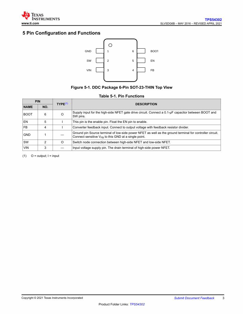
5 Pin Configuration and Functions
1GND 6 BOOT
2SW 5 EN
3VIN 4 FB
Figure 5-1. DDC Package 6-Pin SOT-23-THIN Top View
Table 5-1. Pin FunctionsPIN
TYPE(1) DESCRIPTIONNAME NO.
BOOT 6 O Supply input for the high-side NFET gate drive circuit. Connect a 0.1-μF capacitor between BOOT andSW pins.
EN 5 I This pin is the enable pin. Float the EN pin to enable.
FB 4 I Converter feedback input. Connect to output voltage with feedback resistor divider.
GND 1 — Ground pin Source terminal of low-side power NFET as well as the ground terminal for controller circuit.Connect sensitive VFB to this GND at a single point.
SW 2 O Switch node connection between high-side NFET and low-side NFET.
VIN 3 — Input voltage supply pin. The drain terminal of high-side power NFET.
(1) O = output; I = input
www.ti.comTPS54302
SLVSDG6B – MAY 2016 – REVISED APRIL 2021
Copyright © 2021 Texas Instruments Incorporated Submit Document Feedback 3
Product Folder Links: TPS54302
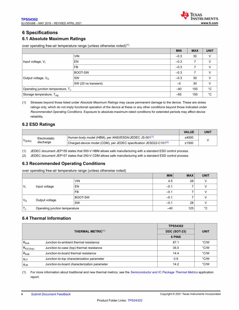
6 Specifications6.1 Absolute Maximum Ratingsover operating free-air temperature range (unless otherwise noted)(1)
MIN MAX UNIT
Input voltage, VI
VIN –0.3 30 V
EN –0.3 7 V
FB –0.3 7 V
Output voltage, VO
BOOT-SW –0.3 7 V
SW –0.3 30 V
SW (20 ns transient) –5 30 V
Operating junction temperature, TJ –40 150 °C
Storage temperature, Tstg –65 150 °C
(1) Stresses beyond those listed under Absolute Maximum Ratings may cause permanent damage to the device. These are stressratings only, which do not imply functional operation of the device at these or any other conditions beyond those indicated underRecommended Operating Conditions. Exposure to absolute-maximum-rated conditions for extended periods may affect devicereliability.
6.2 ESD RatingsVALUE UNIT
V(ESD)Electrostaticdischarge
Human-body model (HBM), per ANSI/ESDA/JEDEC JS-001(1) ±4000V
Charged-device model (CDM), per JEDEC specification JESD22-C101(2) ±1500
(1) JEDEC document JEP155 states that 500-V HBM allows safe manufacturing with a standard ESD control process.(2) JEDEC document JEP157 states that 250-V CDM allows safe manufacturing with a standard ESD control process.
6.3 Recommended Operating Conditionsover operating free-air temperature range (unless otherwise noted)
MIN MAX UNIT
VI Input voltage
VIN 4.5 28 V
EN –0.1 7 V
FB –0.1 7 V
VO Output voltageBOOT-SW –0.1 7 V
SW –0.1 28 V
TJ Operating junction temperature –40 125 °C
6.4 Thermal Information
THERMAL METRIC(1)
TPS54302UNITDDC (SOT-23)
6 PINSRθJA Junction-to-ambient thermal resistance 87.1 °C/W
RθJC(top) Junction-to-case (top) thermal resistance 35.5 °C/W
RθJB Junction-to-board thermal resistance 14.4 °C/W
ψJT Junction-to-top characterization parameter 0.9 °C/W
ψJB Junction-to-board characterization parameter 14.2 °C/W
(1) For more information about traditional and new thermal metrics, see the Semiconductor and IC Package Thermal Metrics applicationreport.
TPS54302SLVSDG6B – MAY 2016 – REVISED APRIL 2021 www.ti.com
4 Submit Document Feedback Copyright © 2021 Texas Instruments Incorporated
Product Folder Links: TPS54302
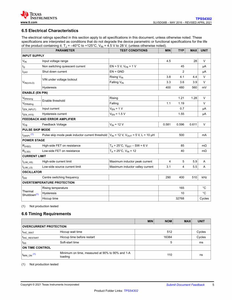
6.5 Electrical CharacteristicsThe electrical ratings specified in this section apply to all specifications in this document, unless otherwise noted. Thesespecifications are interpreted as conditions that do not degrade the device parametric or functional specifications for the lifeof the product containing it. TJ = –40°C to +125°C, VIN = 4.5 V to 28 V, (unless otherwise noted).
PARAMETER TEST CONDITIONS MIN TYP MAX UNITINPUT SUPPLYVIN Input voltage range 4.5 28 V
IQ Non switching quiescent current EN = 5 V, VFB = 1 V 45 µA
IOFF Shut down current EN = GND 2 µA
VIN(UVLO)VIN under voltage lockout
Rising VIN 3.8 4.1 4.4 V
Falling VIN 3.3 3.6 3.9 V
Hysteresis 400 480 560 mV
ENABLE (EN PIN)VENrising Enable threshold
Rising 1.21 1.28 V
VENfalling Falling 1.1 1.19 V
I(EN_INPUT) Input current VEN = 1 V 0.7 μA
I(EN_HYS) Hysteresis current VEN = 1.5 V 1.55 μA
FEEDBACK AND ERROR AMPLIFIERVFB Feedback Voltage VIN = 12 V 0.581 0.596 0.611 V
PULSE SKIP MODEI(SKIP) (1) Pulse skip mode peak inductor current threshold VIN = 12 V, VOUT = 5 V, L = 10 µH 500 mA
POWER STAGER(HSD) High-side FET on resistance TA = 25°C, VBST – SW = 6 V 85 mΩ
R(LSD) Low-side FET on resistance TA = 25°C, VIN = 12 40 mΩ
CURRENT LIMITI(LIM_HS) High-side current limit Maximum inductor peak current 4 5 5.9 A
I(LIM_LS) Low-side source current limit Maximum inductor valley current 3.1 4 5.5 A
OSCILLATORfSW Centre switching frequency 290 400 510 kHz
OVERTEMPERATURE PROTECTION
ThermalShutdown(1)
Rising temperature 165 °C
Hysteresis 10 °C
Hiccup time 32768 Cycles
(1) Not production tested
6.6 Timing RequirementsMIN NOM MAX UNIT
OVERCURRENT PROTECTIONtHIC_WAIT Hiccup wait time 512 Cycles
tHIC_RESTART Hiccup time before restart 16384 Cycles
tSS Soft-start time 5 ms
ON TIME CONTROL
tMIN_ON (1) Minimum on time, measured at 90% to 90% and 1-Aloading 110 ns
(1) Not production tested
www.ti.comTPS54302
SLVSDG6B – MAY 2016 – REVISED APRIL 2021
Copyright © 2021 Texas Instruments Incorporated Submit Document Feedback 5
Product Folder Links: TPS54302
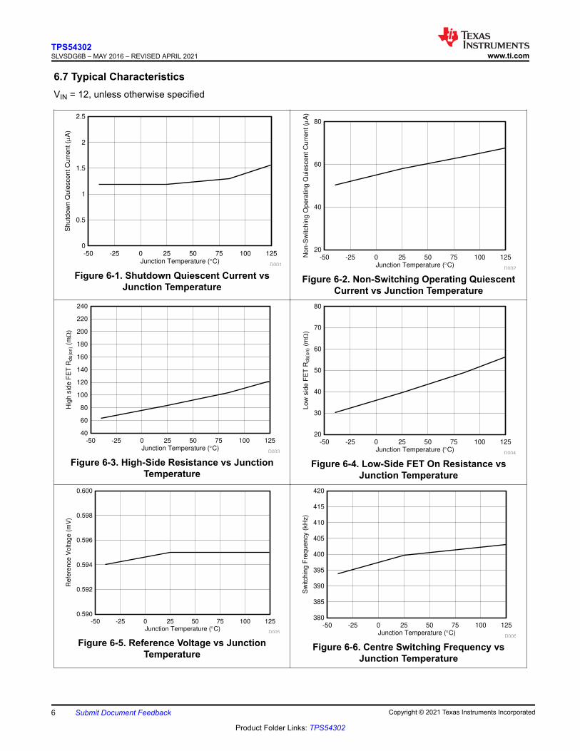
6.7 Typical CharacteristicsVIN = 12, unless otherwise specified
Junction Temperature (qC)
Sh
utd
ow
n Q
uie
sce
nt C
urr
en
t (P
A)
-50 -25 0 25 50 75 100 1250
0.5
1
1.5
2
2.5
D001
Figure 6-1. Shutdown Quiescent Current vsJunction Temperature
Junction Temperature (qC)
No
n-S
witch
ing
Op
era
tin
g Q
uie
sce
nt
Cu
rre
nt (P
A)
-50 -25 0 25 50 75 100 12520
40
60
80
D002
Figure 6-2. Non-Switching Operating QuiescentCurrent vs Junction Temperature
Junction Temperature (qC)
Hig
h s
ide F
ET
Rd
s(o
n) (m:
)
-50 -25 0 25 50 75 100 12540
60
80
100
120
140
160
180
200
220
240
D003
Figure 6-3. High-Side Resistance vs JunctionTemperature
Junction Temperature (qC)
Lo
w s
ide
FE
T R
ds(o
n) (m:
)
-50 -25 0 25 50 75 100 12520
30
40
50
60
70
80
D004
Figure 6-4. Low-Side FET On Resistance vsJunction Temperature
Junction Temperature (qC)
Refe
ren
ce
Voltage
(m
V)
-50 -25 0 25 50 75 100 1250.590
0.592
0.594
0.596
0.598
0.600
D005
Figure 6-5. Reference Voltage vs JunctionTemperature
Junction Temperature (qC)
Sw
itch
ing
Fre
qu
en
cy (
kH
z)
-50 -25 0 25 50 75 100 125380
385
390
395
400
405
410
415
420
D006
Figure 6-6. Centre Switching Frequency vsJunction Temperature
TPS54302SLVSDG6B – MAY 2016 – REVISED APRIL 2021 www.ti.com
6 Submit Document Feedback Copyright © 2021 Texas Instruments Incorporated
Product Folder Links: TPS54302
Junction Temperature (qC)
Hig
h S
ide
Curr
en
t L
imit (
A)
-50 -25 0 25 50 75 100 1252.8
3.3
3.8
4.3
4.8
5.3
5.8
D007
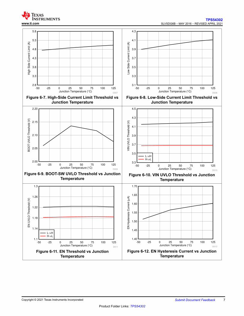
Figure 6-7. High-Side Current Limit Threshold vsJunction Temperature
Junction Temperature (qC)
Low
Sid
e C
urr
ent Lim
it (
A)
-50 -25 0 25 50 75 100 1253.1
3.3
3.5
3.7
3.9
4.1
4.3
D008
Figure 6-8. Low-Side Current Limit Threshold vsJunction Temperature
Junction Temperature (qC)
BO
OT
UV
LO
Th
resh
old
(V
)
-50 -25 0 25 50 75 100 1252.00
2.05
2.10
2.15
2.20
D009
Figure 6-9. BOOT-SW UVLO Threshold vs JunctionTemperature
Junction Temperature (qC)
VIN
UV
LO
Thre
sh
old
(V
)
-50 -25 0 25 50 75 100 1253.3
3.5
3.7
3.9
4.1
4.3
4.5
D010
L->HH->L
Figure 6-10. VIN UVLO Threshold vs JunctionTemperature
Junction Temperature (qC)
EN
UV
LO
Th
resh
old
(V
)
-50 -25 0 25 50 75 100 1251.1
1.14
1.18
1.22
1.26
1.3
D011
L->HH->L
Figure 6-11. EN Threshold vs JunctionTemperature
Junction Temperature (qC)
EN
Hyste
resis
Cu
rre
nt (P
A)
-50 -25 0 25 50 75 100 1251.40
1.45
1.50
1.55
1.60
1.65
1.70
D012
Figure 6-12. EN Hysteresis Current vs JunctionTemperature
www.ti.comTPS54302
SLVSDG6B – MAY 2016 – REVISED APRIL 2021
Copyright © 2021 Texas Instruments Incorporated Submit Document Feedback 7
Product Folder Links: TPS54302
7 Detailed Description7.1 OverviewThe TPS54302 device is a 28-V, 3-A, synchronous step-down (buck) converter with two integrated n-channelMOSFETs. To improve performance during line and load transients the device implements a constant-frequency,peak current-mode control which reduces output capacitance. The optimized internal compensation networkminimizes the external component counts and simplifies the control loop design.
The switching frequency of the device is fixed to 400 kHz.
The TPS54302 device starts switching when VIN is 4.5 V. The operating current is 45 μA (typical) when notswitching and under no load. When the device is disabled, the supply current is 2 µA (typical).
The integrated 85-mΩ high-side MOSFET and 40-mΩ low-side MOSFET allow for high-efficiency power-supplydesigns with continuous output currents up to 3 A.
The TPS54302 device reduces the external component count by integrating the boot recharge diode. The biasvoltage for the integrated high-side MOSFET is supplied by an external capacitor on the BOOT to PH pins. Theboot capacitor voltage is monitored by an UVLO circuit and turns off the high-side MOSFET when the voltagefalls below a preset threshold of 2.1 V (typical).
The device minimizes excessive output overvoltage transients by taking advantage of the overvoltagecomparator. When the regulated output voltage is greater than 108% of the nominal voltage, the overvoltagecomparator is activated, and the high-side MOSFET is turned off and masked from turning on until the outputvoltage is lower than 104%.
The TPS54302 device has internal 5-ms soft-start time to minimize inrush currents.
TPS54302SLVSDG6B – MAY 2016 – REVISED APRIL 2021 www.ti.com
8 Submit Document Feedback Copyright © 2021 Texas Instruments Incorporated
Product Folder Links: TPS54302
7.2 Functional Block Diagram
FB
Voltage
ReferenceHS MOSFET
Current
Comparator
Slope
Compensation
Overload
Recovery
Maximum
ClampOscillator
Power Stage
and Dead Time
Control Logic
LS MOSFET
Current Limit
Maximum Clamp
Pulse Skip
Overvoltage
Comparator
Boot
UVLO
Regulator
VIN
Boot Charge
GND
BOOT
SW
Current
Sense
Current
Sense
IN
IhIp
EN
Enable
Comparator
Shutdown
Logic
Thermal Hiccup
UVLO
Hiccup
Shutdown
Hiccup
Shutdown
+
±
+
±
+
Soft Start
2.04 nF
20 k
Error
Amplifier
2 pF
Copyright © 2017, Texas Instruments Incorporated
7.3 Feature Description7.3.1 Fixed-Frequency PWM Control
The device uses a fixed-frequency, peak current-mode control. The output voltage is compared through externalresistors on the FB pin to an internal voltage reference by an error amplifier. An internal oscillator initiates theturnon of the high-side power switch. The error amplifier output is compared to the current of the high-sidepower switch. When the power-switch current reaches the error amplifier output voltage level, the high-sidepower switch is turned off and the low-side power switch is turned on. The error amplifier output voltageincreases and decreases as the output current increases and decreases. The device implements a current-limitby clamping the error amplifier voltage to a maximum level and also implements a minimum clamp for improvedtransient-response performance.
7.3.2 Pulse Skip Mode
The TPS54302 device is designed to operate in pulse-skipping mode at light-load currents to boost light-loadefficiency. When the peak inductor current is lower than 500 mA (typical), the device enters pulse-skippingmode. When the device is in pulse-skipping mode, the error amplifier output voltage is clamped which preventsthe high-side integrated MOSFET from switching. The peak inductor current must rise above 500 mA and exit
www.ti.comTPS54302
SLVSDG6B – MAY 2016 – REVISED APRIL 2021
Copyright © 2021 Texas Instruments Incorporated Submit Document Feedback 9
Product Folder Links: TPS54302
pulse skip mode. Because the integrated current comparator catches the peak inductor current only, the averageload current entering pulse-skipping mode varies with the applications and external output filters.
7.3.3 Error Amplifier
The device has a transconductance amplifier as the error amplifier. The error amplifier compares the FB voltageto the lower of the internal soft-start voltage or the internal 0.596-V voltage reference. The transconductance ofthe error amplifier is 240 µA/V (typical). The frequency compensation components are placed internal betweenthe output of the error amplifier and ground.
7.3.4 Slope Compensation and Output Current
The device adds a compensating ramp to the signal of the switch current. This slope compensation preventssub-harmonic oscillations as the duty cycle increases. The available peak inductor current remains constant overthe full duty-cycle range.
7.3.5 Enable and Adjusting Undervoltage Lockout
The EN pin provides electrical on and off control of the device. When the EN pin voltage exceeds the thresholdvoltage, the device begins operation. If the EN pin voltage is pulled below the threshold voltage, the regulatorstops switching and enters the low-quiescent (IQ) state.
The EN pin has an internal pullup-current source which allows the user to float the EN pin to enable the device.If an application requires control of the EN pin, use open-drain or open-collector output logic to interface with thepin.
The device implements internal undervoltage-lockout (UVLO) circuitry on the VIN pin. The device is disabledwhen the VIN pin voltage falls below the internal VIN UVLO threshold. The internal VIN UVLO threshold has ahysteresis of 480 mV.
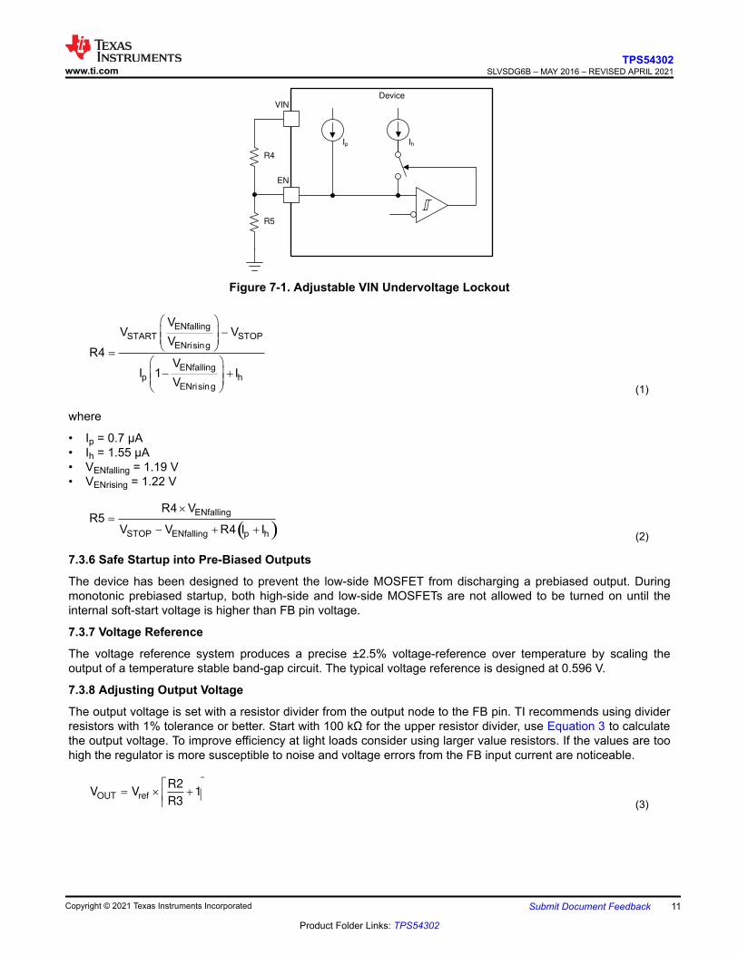
If an application requires a higher UVLO threshold on the VIN pin, then the EN pin can be configured as shownin Figure 7-1. When using the external UVLO function, setting the hysteresis at a value greater than 500 mV isrecommended.
The EN pin has a small pullup current, Ip, which sets the default state of the pin to enable when no externalcomponents are connected. The pullup current is also used to control the voltage hysteresis for the UVLOfunction because it increases by Ih when the EN pin crosses the enable threshold. Use Equation 1 and Equation2 to calculate the values of R4 and R5 for a specified UVLO threshold.
TPS54302SLVSDG6B – MAY 2016 – REVISED APRIL 2021 www.ti.com
10 Submit Document Feedback Copyright © 2021 Texas Instruments Incorporated
Product Folder Links: TPS54302
Device
EN
Ip
VIN
R4
R5
Ih
Figure 7-1. Adjustable VIN Undervoltage Lockout
ENfallingSTART STOP
ENrising
ENfallingp h
ENrising
VV V
VR4
VI 1 I
V
æ ö-ç ÷
ç ÷è ø=
æ ö- +ç ÷
ç ÷è ø (1)
where
• Ip = 0.7 µA• Ih = 1.55 µA• VENfalling = 1.19 V• VENrising = 1.22 V
( )ENfalling
STOP ENfalling p h
R4 VR5
V V R4 I I
´=
- + + (2)
7.3.6 Safe Startup into Pre-Biased Outputs
The device has been designed to prevent the low-side MOSFET from discharging a prebiased output. Duringmonotonic prebiased startup, both high-side and low-side MOSFETs are not allowed to be turned on until theinternal soft-start voltage is higher than FB pin voltage.
7.3.7 Voltage Reference
The voltage reference system produces a precise ±2.5% voltage-reference over temperature by scaling theoutput of a temperature stable band-gap circuit. The typical voltage reference is designed at 0.596 V.
7.3.8 Adjusting Output Voltage
The output voltage is set with a resistor divider from the output node to the FB pin. TI recommends using dividerresistors with 1% tolerance or better. Start with 100 kΩ for the upper resistor divider, use Equation 3 to calculatethe output voltage. To improve efficiency at light loads consider using larger value resistors. If the values are toohigh the regulator is more susceptible to noise and voltage errors from the FB input current are noticeable.
OUT ref
R2V V 1
R3
ª º u �« »
¬ ¼ (3)
www.ti.comTPS54302
SLVSDG6B – MAY 2016 – REVISED APRIL 2021
Copyright © 2021 Texas Instruments Incorporated Submit Document Feedback 11
Product Folder Links: TPS54302
7.3.9 Internal Soft-Start
The TPS54302 device uses the internal soft-start function. The internal soft start time is set to 5 ms (typical).
7.3.10 Bootstrap Voltage (BOOT)
The TPS54302 device has an integrated boot regulator and requires a 0.1-µF ceramic capacitor between theBOOT and SW pins to provide the gate-drive voltage for the high-side MOSFET. A ceramic capacitor withan X7R or X5R grade dielectric is recommended because of the stable characteristics over temperature andvoltage. To improve drop out, the TPS54302 device is designed to operate at 100% duty cycle as long as theBOOT to SW pin voltage is greater than 2.1 V (typical).
7.3.11 Overcurrent Protection
The device is protected from overcurrent conditions by cycle-by-cycle current limiting on both the high-sideMOSFET and the low-side MOSFET.
7.3.11.1 High-Side MOSFET Overcurrent Protection
The device implements current-mode control which uses the internal COMP voltage to control the turnoff of thehigh-side MOSFET and the turnon of the low-side MOSFET on a cycle-by-cycle basis. During each cycle, theswitch current and the current reference generated by the internal COMP voltage are compared. When the peakswitch current intersects the current reference the high-side switch turns off.
7.3.11.2 Low-Side MOSFET Overcurrent Protection
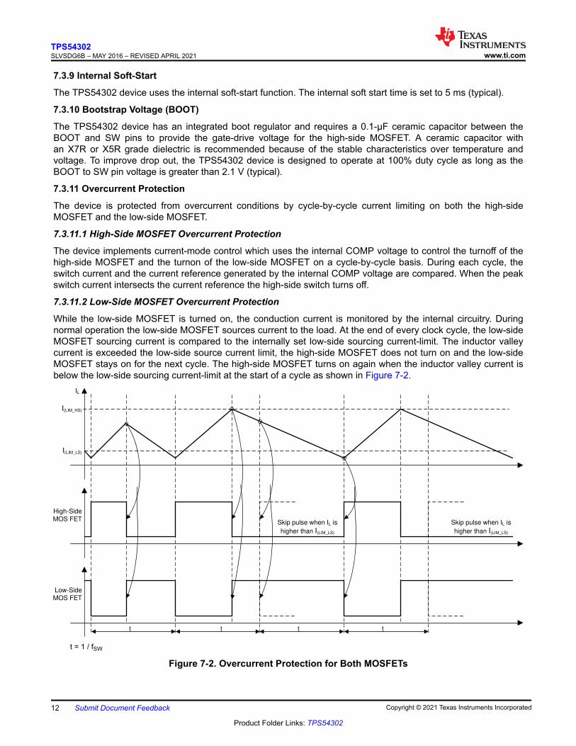
While the low-side MOSFET is turned on, the conduction current is monitored by the internal circuitry. Duringnormal operation the low-side MOSFET sources current to the load. At the end of every clock cycle, the low-sideMOSFET sourcing current is compared to the internally set low-side sourcing current-limit. The inductor valleycurrent is exceeded the low-side source current limit, the high-side MOSFET does not turn on and the low-sideMOSFET stays on for the next cycle. The high-side MOSFET turns on again when the inductor valley current isbelow the low-side sourcing current-limit at the start of a cycle as shown in Figure 7-2.
I(LIM_HS)
I(LIM_LS)
IL
High-Side
MOS FET
Low-Side
MOS FET
Skip pulse when IL is
higher than I(LIM_LS)
Skip pulse when IL is
higher than I(LIM_LS)
t t t t
t = 1 / fSW
Figure 7-2. Overcurrent Protection for Both MOSFETs
TPS54302SLVSDG6B – MAY 2016 – REVISED APRIL 2021 www.ti.com
12 Submit Document Feedback Copyright © 2021 Texas Instruments Incorporated
Product Folder Links: TPS54302
Furthermore, if an output overload condition occurs for more than the hiccup wait time, which is programmed for512 switching cycles, the device shuts down and restarts after the hiccup time of 16384 cycles. The hiccup modehelps to reduce the device power dissipation under severe overcurrent conditions.
7.3.12 Spread Spectrum
To reduce EMI, the TPS54302 device introduces frequency spread spectrum. The jittering span is ±6% of theswitching frequency with 1/512 swing frequency.
7.3.13 Output Overvoltage Protection (OVP)
The TPS54302 incorporates an overvoltage transient protection (OVTP) circuit to minimize output voltageovershoot when recovering from output fault conditions or strong unload transients. The OVTP circuit includesan overvoltage comparator to compare the FB pin voltage and internal thresholds. When the FB pin voltage goesabove 108% × Vref, the high-side MOSFET is forced off. When the FB pin voltage falls below 104% × Vref, thehigh-side MOSFET is enabled again.
7.3.14 Thermal Shutdown
The internal thermal-shutdown circuitry forces the device to stop switching if the junction temperature exceeds165°C (typical). When the junction temperature drops below 155°C (typical), the internal thermal-hiccup timerbegins to count. The device reinitiates the power-up sequence after the built-in thermal-shutdown hiccup time(32768 cycles) is over.
7.4 Device Functional Modes7.4.1 Normal Operation
When the input voltage is above the UVLO threshold, the TPS54302 device can operate in normal switchingmodes. Normal continuous conduction mode (CCM) occurs when inductor peak current is above 0 A. In CCM,the TPS54302 device operates at a fixed frequency.
7.4.2 Eco-mode™ Operation
The device is designed to operate in high-efficiency pulse-skipping mode under light-load conditions. Pulseskipping initiates when the switch current falls to 500 mA (typical). During pulse skipping, the low-side FET turnsoff when the switch current falls to 0 A. The switching node (the SW pin) waveform takes on the characteristicsof discontinuous conduction mode (DCM) operation and the apparent switching frequency decreases. As theoutput current decreases, the perceived time between switching pulses increases.
www.ti.comTPS54302
SLVSDG6B – MAY 2016 – REVISED APRIL 2021
Copyright © 2021 Texas Instruments Incorporated Submit Document Feedback 13
Product Folder Links: TPS54302

8 Application and ImplementationNote
Information in the following applications sections is not part of the TI component specification,and TI does not warrant its accuracy or completeness. TI’s customers are responsible fordetermining suitability of components for their purposes, as well as validating and testing their designimplementation to confirm system functionality.
8.1 Application InformationThe TPS54302 device is typically used as a step-down converter, which converts an input voltage from 8 V to 28V to a fixed output voltage of 5 V.
8.2 Typical Application8.2.1 TPS54302 8-V to 28-V Input, 5-V Output Converter
VIN
EN
GND
BOOT
FB
SW
VIN
VOUT
L110 µH
3
1
5
2
4
6
C110 µF
C30.1 µF
R149.9
R313.3 k
C675 pF
U1TPS54302
VIN = 8 V to ~28 V
C20.1 µF
R4511 k
R5105 k
R2100 k
C422 µF
C522 µF
VOUT = 5 V, 3 A
Copyright © 2017, Texas Instruments Incorporated
Figure 8-1. 5-V, 3-A Reference Design
8.2.2 Design Requirements
For this design example, use the parameters in Table 8-1.
Table 8-1. Design ParametersPARAMETER VALUE
Input voltage range 8 V to 28 V
Output voltage 5 V
Output current 3 A
Transient response, 1.5-A load step ΔVOUT = ±5 %
Input ripple voltage 400 mV
Output voltage ripple 30 mVPP
Switching frequency 400 kHz
TPS54302SLVSDG6B – MAY 2016 – REVISED APRIL 2021 www.ti.com
14 Submit Document Feedback Copyright © 2021 Texas Instruments Incorporated
Product Folder Links: TPS54302
8.2.3 Detailed Design Procedure8.2.3.1 Input Capacitor Selection
The device requires an input decoupling capacitor and a bulk capacitor is needed depending on the application.A ceramic capacitor over 10 µF is recommended for the decoupling capacitor. An additional 0.1-µF capacitor(C2) from the VIN pin to GND is optional to provide additional high frequency filtering. The capacitor voltagerating must be greater than the maximum input voltage.
Use Equation 4 to calculate the input ripple voltage (ΔVIN).
( )( )( )OUT MAX
IN MAXOUT MAX
BULK sw
I 0.25
V I ESRC f
´D = + ´
´ (4)
where
• CBULK is the bulk capacitor value.• fSW is the switching frequency.• IOUT(MAX) is the maximum loading current.• ESRMAX is maximum series resistance of the bulk capacitor.
The maximum RMS (root mean square) ripple current must also be checked. For worst case conditions, useEquation 5 to calculate ICIN(RMS).
OUT(MAX)CIN(RMS)
II
2
(5)
The actual input-voltage ripple is greatly affected by parasitic associated with the layout and the outputimpedance of the voltage source. The Section 8.2.2 show the actual input voltage ripple for this circuit whichis larger than the calculated value. This measured value is still below the specified input limit of 400 mV. Themaximum voltage across the input capacitors is VINmax + ΔVIN / 2. The selected bypass capacitor is rated for 35V and the ripple current capacity is greater than 2 A. Both values provide ample margin. The maximum ratingsfor voltage and current must not be exceeded under any circumstance.
8.2.3.2 Bootstrap Capacitor Selection
A 0.1-µF ceramic capacitor must be connected between the BOOT to SW pin for proper operation. TIrecommends using a ceramic capacitor.
8.2.3.3 Output Voltage Set Point
The output voltage of the TPS54302 device is externally adjustable using a resistor divider network. In theapplication circuit of Figure 8-1, this divider network comprises R2 and R3. Use Equation 6 and Equation 7 tocalculate the relationship of the output voltage to the resistor divider.
ref
OUT ref
R2 VR3
V V
´
=
- (6)
OUT ref
R2V V 1
R3
ª º u �« »
¬ ¼ (7)
Select a value of R2 to be approximately 100 kΩ. Slightly increasing or decreasing the value of R3 can result incloser output voltage matching when using standard value resistors. In this design, R2 = 100 kΩ and R3 = 13.3kΩ which results in a 5-V output voltage. The 49.9-Ω resistor, R1, is provided as a convenient location to breakthe control loop for stability testing.
www.ti.comTPS54302
SLVSDG6B – MAY 2016 – REVISED APRIL 2021
Copyright © 2021 Texas Instruments Incorporated Submit Document Feedback 15
Product Folder Links: TPS54302
8.2.3.4 Undervoltage Lockout Set Point
The undervoltage lockout (UVLO) set point can be adjusted using the external-voltage divider network of R4and R5. The R4 resistor is connected between the VIN and EN pins of the TPS54302 device. The R5 resistoris connected between the EN and GND pins. The UVLO has two thresholds, one for power up when the inputvoltage is rising and one for power down or brownouts when the input voltage is falling. For the example design,the minimum input voltage is 8 V, so the start voltage threshold is set to 6.74 V and the stop voltage threshold isset to 5.83 V. Use Equation 1 and Equation 2 to calculate the values for the upper and lower resistor values ofR4 and R5.
8.2.3.5 Output Filter Components
Two components must be selected for the output filter: the output inductor (LO) and CO.
8.2.3.5.1 Inductor Selection
Use Equation 8 to calculate the minimum value of the output inductor (LMIN).
( )( )( )
OUT OUTIN MAX
IND OUT swIN
MIN
MAX
V V V
V fL
K I
´ -=
´ ´ ´(8)
where
• KIND is a coefficient that represents the amount of inductor ripple current relative to the maximum outputcurrent.
In general, the value of KIND is at the discretion of the designer; however, the following guidelines may be used.For designs using low-ESR output capacitors, such as ceramics, a higher KIND can be used. When using higherESR output capacitors, KIND = 0.2 yields better results.
For this design example, use KIND = 0.35. The minimum inductor value is calculated as 9.78 μH. For this design,a close standard value of 10 μH was selected for LMIN.
For the output filter inductor, the RMS current and saturation current ratings must not be exceeded. UseEquation 9 to calculate the RMS inductor current (IL(RMS)).
� �� �� �
� �
2
OUT OUTIN MAX2OUT MAX
O SWIN MAL( AX
XM )
V V V1
I12 V L f 0.8
I
§ ·u �¨ ¸ � u ¨ ¸u u u¨ ¸
© ¹ (9)
Use Equation 10 to calculate the peak inductor current (IL(PK)).
� �� �� �
� �
OUT OUTIN MA
L(
X
OUT MAXO SWIN MA
PK)X
V V VI
1.6 V LI
f
u � �
u u u(10)
Smaller or larger inductor values can be used depending on the amount of ripple current the designer wants toallow so long as the other design requirements are met. Larger value inductors have lower AC current and resultin lower output voltage ripple. Smaller inductor values increase AC current and output voltage ripple.
8.2.3.5.2 Output Capacitor Selection
Consider three primary factors when selecting the value of the output capacitor. The output capacitor determinesthe modulator pole, the output voltage ripple, and how the regulator responds to a large change in load current.The output capacitance must be selected based on the more stringent of these three criteria.
The desired response to a large change in the load current is the first criterion. The output capacitor must supplythe load with current when the regulator cannot. This situation occurs if the desired hold-up times are present for
TPS54302SLVSDG6B – MAY 2016 – REVISED APRIL 2021 www.ti.com
16 Submit Document Feedback Copyright © 2021 Texas Instruments Incorporated
Product Folder Links: TPS54302
the regulator. In this case, the output capacitor must hold the output voltage above a certain level for a specifiedamount of time after the input power is removed. The regulator is also temporarily unable to supply sufficientoutput current if a large, fast increase occurs affecting the current requirements of the load, such as a transitionfrom no load to full load. The regulator usually requires two or more clock cycles for the control loop to noticethe change in load current and output voltage and to adjust the duty cycle to react to the change. The outputcapacitor must be sized to supply the extra current to the load until the control loop responds to the load change.The output capacitance must be large enough to supply the difference in current for 2 clock cycles while onlyallowing a tolerable amount of drop in the output voltage. Use Equation 11 to calculate the minimum requiredoutput capacitance.
OUTO
sw OUT
2 IC
f V
u '!
u ' (11)
where
• ∆IOUT is the change in output current.• fSW is the switching frequency of the regulator.• ∆VOUTb is the allowable change in the output voltage.
For this example, the transient load response is specified as a 5% change in the output voltage, VOUT, for a loadstep of 1.5 A. For this example, ΔIOUT = 1.5 A and ΔVOUT = 0.05 × 5 = 0.25 V. Using these values results ina minimum capacitance of 30 μF. This value does not consider the ESR of the output capacitor in the outputvoltage change. For ceramic capacitors, the ESR is usually small enough to ignore in this calculation.
Use Equation 12 to calculate the minimum output capacitance required to meet the output voltage ripplespecification. In this case, the maximum output voltage ripple is 30 mV. Under this requirement, Equation 12yields 10.7 μF.
OOUTrippleSW
ripple
1 1C
V8 f
I
´
> ´
(12)
where
• ƒSW is the switching frequency.• VOUTripple is the maximum allowable output voltage ripple.• Iripple is the inductor ripple current
Use Equation 13 to calculate the maximum ESR an output capacitor can have to meet the output-voltage ripplespecification. Equation 13 indicates the ESR should be less than 29.2 mΩ. In this case, the ESR of the ceramiccapacitor is much smaller than 29.2 mΩ.
OUTrippleESR
ripple
VR
I<
(13)
The output capacitor can affect the crossover frequency fo. Considering the loop stability and effect of theinternal parasitic parameters, choose the crossover frequency less than 40 kHz without considering the feedforward capacitor. A simple estimation for the crossover frequency without feed forward capacitor C6 is shown inEquation 14, assuming CO has small ESR.
oOUT O
5.1f =
V
Cu (14)
Additional capacitance deratings for aging, temperature, and DC bias should be considered which increasesthis minimum value. For this example, two 22-uF 25-V, X7R ceramic capacitors are used. Capacitors generallyhave limits to the amount of ripple current they can handle without failing or producing excess heat. An output
www.ti.comTPS54302
SLVSDG6B – MAY 2016 – REVISED APRIL 2021
Copyright © 2021 Texas Instruments Incorporated Submit Document Feedback 17
Product Folder Links: TPS54302
capacitor that can support the inductor ripple current must be specified. Some capacitor data sheets specify theRMS value of the maximum ripple current. Use Equation 15 to calculate the RMS ripple current that the outputcapacitor must support. For this application, Equation 15 yields 296 mA for each capacitor.
� �� �� �
� �
OUT OUTIN MAX
COUT RMSO SW CIN MAX
V V V1
IV L f N12
§ ·u �¨ ¸ u ¨ ¸u u u¨ ¸
© ¹ (15)
8.2.3.5.3 Feedforward Capacitor
The TPS54302 device is internally compensated and the internal compensation network is composed of twocapacitors and one resister shown on the Section 7.2. Depending on the VOUT, if the output capacitor COUT isdominated by low ESR (ceramic types) capacitors, it could result in low phase margin. To improve the phaseboost an external feedforward capacitor C6 can be added in parallel with R2. The C6 capacitor is chosen suchthat phase margin is boosted at the crossover frequency.
Equation 16 for C6 was tested.
o
1 1C6 =
2 f R2u
S (16)
For this design, C6 = 75 pF. The C6 capacitor is not needed when COUT has high ESR, and C6 calculated fromEquation 16 should be reduced with medium ESR. Table 8-2 can be used as a starting point.
Table 8-2 lists some recommended component values.
Table 8-2. Recommended Component ValuesVOUT (V) L (µH) COUT (µF) R2 (kΩ) R3 (kΩ) C8 (pF)
1.8 4.7 66 100 49.9 33
2.5 5.6 66 100 31.6 47
3.3 6.8 44 100 22.1 47
5 10 44 100 13.3 75
12 15 44 100 5.23 100
TPS54302SLVSDG6B – MAY 2016 – REVISED APRIL 2021 www.ti.com
18 Submit Document Feedback Copyright © 2021 Texas Instruments Incorporated
Product Folder Links: TPS54302
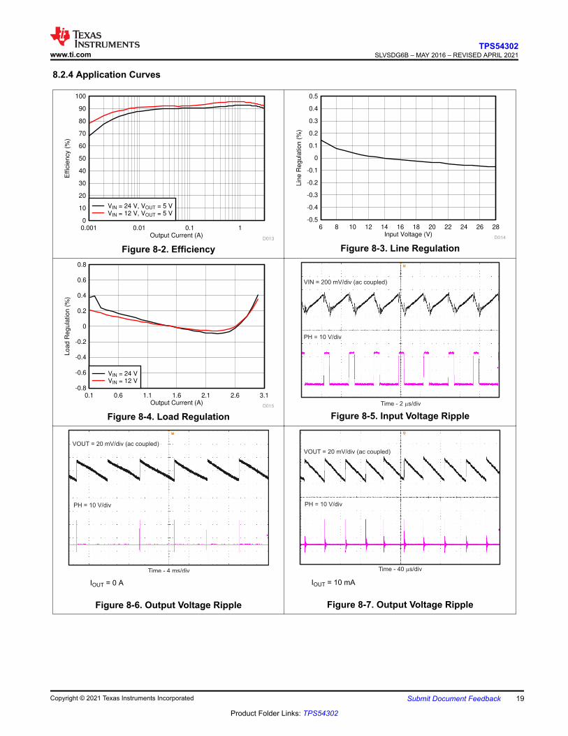
8.2.4 Application Curves
Output Current (A)
Effic
iency (
%)
0
10
20
30
40
50
60
70
80
90
100
0.001 0.01 0.1 1
D013
VIN = 24 V, VOUT = 5 VVIN = 12 V, VOUT = 5 V
Figure 8-2. EfficiencyInput Voltage (V)
Lin
e R
egu
latio
n (
%)
6 8 10 12 14 16 18 20 22 24 26 28-0.5
-0.4
-0.3
-0.2
-0.1
0
0.1
0.2
0.3
0.4
0.5
D014
Figure 8-3. Line Regulation
Output Current (A)
Lo
ad
Re
gu
latio
n (
%)
0.1 0.6 1.1 1.6 2.1 2.6 3.1-0.8
-0.6
-0.4
-0.2
0
0.2
0.4
0.6
0.8
D015
VIN = 24 VVIN = 12 V
Figure 8-4. Load Regulation
VIN = 200 mV/div (ac coupled)
PH = 10 V/div
Time - 2 s/divm
Figure 8-5. Input Voltage Ripple
VOUT = 20 mV/div (ac coupled)
PH = 10 V/div
Time - 4 ms/div
IOUT = 0 A
Figure 8-6. Output Voltage Ripple
VOUT = 20 mV/div (ac coupled)
PH = 10 V/div
Time - 40 s/divm
IOUT = 10 mA
Figure 8-7. Output Voltage Ripple
www.ti.comTPS54302
SLVSDG6B – MAY 2016 – REVISED APRIL 2021
Copyright © 2021 Texas Instruments Incorporated Submit Document Feedback 19
Product Folder Links: TPS54302
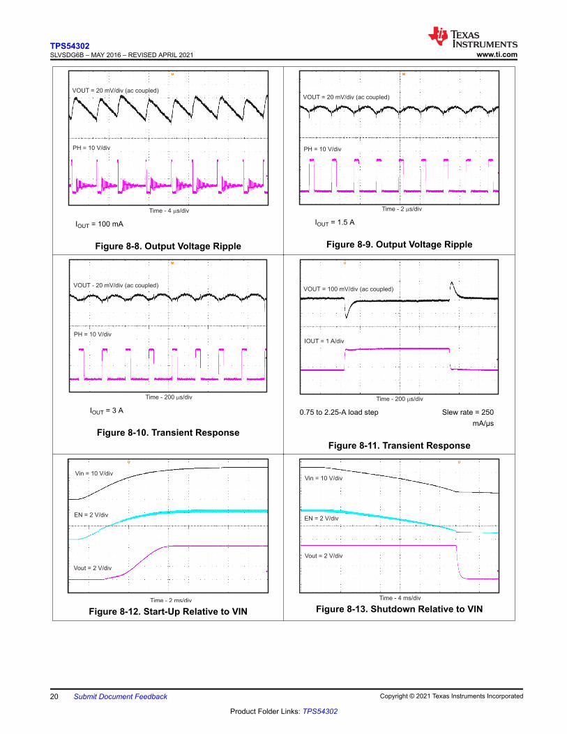
VOUT = 20 mV/div (ac coupled)
PH = 10 V/div
Time - 4 s/divm
IOUT = 100 mA
Figure 8-8. Output Voltage Ripple
VOUT = 20 mV/div (ac coupled)
PH = 10 V/div
Time - 2 s/divm
IOUT = 1.5 A
Figure 8-9. Output Voltage Ripple
VOUT - 20 mV/div (ac coupled)
PH = 10 V/div
Time - 200 s/divm
IOUT = 3 A
Figure 8-10. Transient Response
VOUT = 100 mV/div (ac coupled)
IOUT = 1 A/div
Time - 200 s/divm
0.75 to 2.25-A load step Slew rate = 250mA/μs
Figure 8-11. Transient Response
Vin = 10 V/div
EN = 2 V/div
Vout = 2 V/div
Time - 2 ms/div
Figure 8-12. Start-Up Relative to VIN
Vin = 10 V/div
EN = 2 V/div
Vout = 2 V/div
Time - 4 ms/div
Figure 8-13. Shutdown Relative to VIN
TPS54302SLVSDG6B – MAY 2016 – REVISED APRIL 2021 www.ti.com
20 Submit Document Feedback Copyright © 2021 Texas Instruments Incorporated
Product Folder Links: TPS54302
Vin = 10 V/div
EN = 2 V/div
Vout = 2 V/div
Time - 2 ms/div
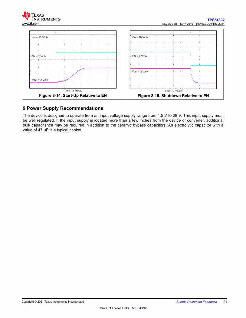
Figure 8-14. Start-Up Relative to EN
Vout = 2 V/div
EN = 2 V/div
Vin = 10 V/div
Time - 2 ms/div
Figure 8-15. Shutdown Relative to EN
9 Power Supply RecommendationsThe device is designed to operate from an input voltage supply range from 4.5 V to 28 V. This input supply mustbe well regulated. If the input supply is located more than a few inches from the device or converter, additionalbulk capacitance may be required in addition to the ceramic bypass capacitors. An electrolytic capacitor with avalue of 47 µF is a typical choice.
www.ti.comTPS54302
SLVSDG6B – MAY 2016 – REVISED APRIL 2021
Copyright © 2021 Texas Instruments Incorporated Submit Document Feedback 21
Product Folder Links: TPS54302
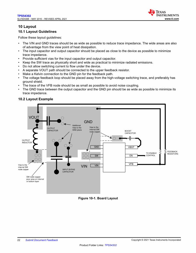
10 Layout10.1 Layout GuidelinesFollow these layout guidelines:
• The VIN and GND traces should be as wide as possible to reduce trace impedance. The wide areas are alsoof advantage from the view point of heat dissipation.
• The input capacitor and output capacitor should be placed as close to the device as possible to minimizetrace impedance.
• Provide sufficient vias for the input capacitor and output capacitor.• Keep the SW trace as physically short and wide as practical to minimize radiated emissions.• Do not allow switching current to flow under the device.• A separate VOUT path should be connected to the upper feedback resistor.• Make a Kelvin connection to the GND pin for the feedback path.• The voltage feedback loop should be placed away from the high-voltage switching trace, and preferably has
ground shield.• The trace of the VFB node should be as small as possible to avoid noise coupling.• The GND trace between the output capacitor and the GND pin should be as wide as possible to minimize its
trace impedance.
10.2 Layout Example
EN
VFB
VBSTGND
SW
FEEDBACK
RESISTORSTO ENABLE
CONTROL
VIN
GND
BOOST
CAPACITOR
OUTPUT
INDUCTOR
OUTPUT
CAPACITOR
VOUT
INPUT BYPAS
CAPACITOR
VIN
SW node copper
pour area on internal
or bottom layer
Additional
Vias to the
GND plane
Vias to the
internal SW
node copper
Vias to the
internal SW
node copper
Figure 10-1. Board Layout
TPS54302SLVSDG6B – MAY 2016 – REVISED APRIL 2021 www.ti.com
22 Submit Document Feedback Copyright © 2021 Texas Instruments Incorporated
Product Folder Links: TPS54302
11 Device and Documentation Support11.1 Device Support11.1.1 Third-Party Products Disclaimer
TI'S PUBLICATION OF INFORMATION REGARDING THIRD-PARTY PRODUCTS OR SERVICES DOES NOTCONSTITUTE AN ENDORSEMENT REGARDING THE SUITABILITY OF SUCH PRODUCTS OR SERVICESOR A WARRANTY, REPRESENTATION OR ENDORSEMENT OF SUCH PRODUCTS OR SERVICES, EITHERALONE OR IN COMBINATION WITH ANY TI PRODUCT OR SERVICE.
11.2 Receiving Notification of Documentation UpdatesTo receive notification of documentation updates, navigate to the device product folder on ti.com. Click onSubscribe to updates to register and receive a weekly digest of any product information that has changed. Forchange details, review the revision history included in any revised document.
11.3 Support ResourcesTI E2E™ support forums are an engineer's go-to source for fast, verified answers and design help — straightfrom the experts. Search existing answers or ask your own question to get the quick design help you need.
Linked content is provided "AS IS" by the respective contributors. They do not constitute TI specifications and donot necessarily reflect TI's views; see TI's Terms of Use.
11.4 TrademarksEco-mode™ and TI E2E™ are trademarks of Texas Instruments.All trademarks are the property of their respective owners.11.5 Electrostatic Discharge Caution
This integrated circuit can be damaged by ESD. Texas Instruments recommends that all integrated circuits be handledwith appropriate precautions. Failure to observe proper handling and installation procedures can cause damage.ESD damage can range from subtle performance degradation to complete device failure. Precision integrated circuits maybe more susceptible to damage because very small parametric changes could cause the device not to meet its publishedspecifications.
11.6 GlossaryTI Glossary This glossary lists and explains terms, acronyms, and definitions.
12 Mechanical, Packaging, and Orderable InformationThe following pages include mechanical, packaging, and orderable information. This information is the mostcurrent data available for the designated devices. This data is subject to change without notice and revision ofthis document. For browser-based versions of this data sheet, refer to the left-hand navigation.
www.ti.comTPS54302
SLVSDG6B – MAY 2016 – REVISED APRIL 2021
Copyright © 2021 Texas Instruments Incorporated Submit Document Feedback 23
Product Folder Links: TPS54302
PACKAGE OPTION ADDENDUM
www.ti.com 10-Dec-2020
Addendum-Page 1
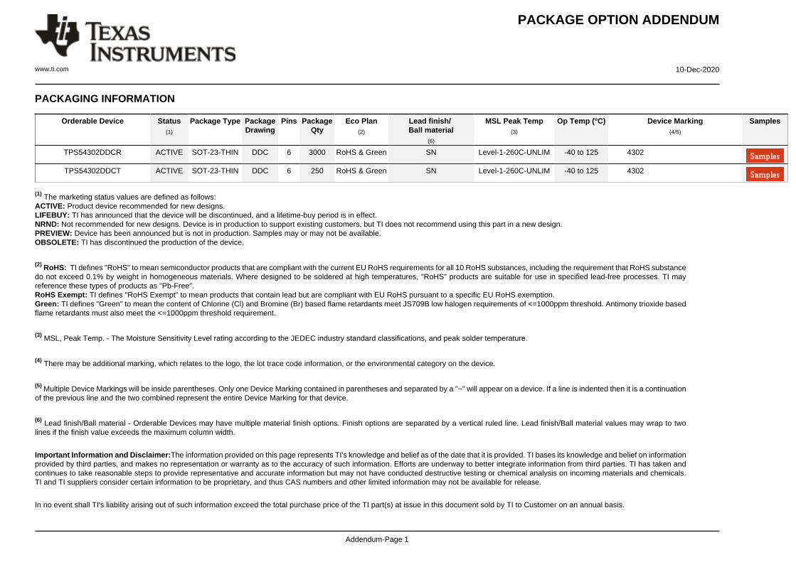
PACKAGING INFORMATION
Orderable Device Status(1)
Package Type PackageDrawing
Pins PackageQty
Eco Plan(2)
Lead finish/Ball material
(6)
MSL Peak Temp(3)
Op Temp (°C) Device Marking(4/5)
Samples
TPS54302DDCR ACTIVE SOT-23-THIN DDC 6 3000 RoHS & Green SN Level-1-260C-UNLIM -40 to 125 4302
TPS54302DDCT ACTIVE SOT-23-THIN DDC 6 250 RoHS & Green SN Level-1-260C-UNLIM -40 to 125 4302
(1) The marketing status values are defined as follows:ACTIVE: Product device recommended for new designs.LIFEBUY: TI has announced that the device will be discontinued, and a lifetime-buy period is in effect.NRND: Not recommended for new designs. Device is in production to support existing customers, but TI does not recommend using this part in a new design.PREVIEW: Device has been announced but is not in production. Samples may or may not be available.OBSOLETE: TI has discontinued the production of the device.
(2) RoHS: TI defines "RoHS" to mean semiconductor products that are compliant with the current EU RoHS requirements for all 10 RoHS substances, including the requirement that RoHS substancedo not exceed 0.1% by weight in homogeneous materials. Where designed to be soldered at high temperatures, "RoHS" products are suitable for use in specified lead-free processes. TI mayreference these types of products as "Pb-Free".RoHS Exempt: TI defines "RoHS Exempt" to mean products that contain lead but are compliant with EU RoHS pursuant to a specific EU RoHS exemption.Green: TI defines "Green" to mean the content of Chlorine (Cl) and Bromine (Br) based flame retardants meet JS709B low halogen requirements of <=1000ppm threshold. Antimony trioxide basedflame retardants must also meet the <=1000ppm threshold requirement.
(3) MSL, Peak Temp. - The Moisture Sensitivity Level rating according to the JEDEC industry standard classifications, and peak solder temperature.
(4) There may be additional marking, which relates to the logo, the lot trace code information, or the environmental category on the device.
(5) Multiple Device Markings will be inside parentheses. Only one Device Marking contained in parentheses and separated by a "~" will appear on a device. If a line is indented then it is a continuationof the previous line and the two combined represent the entire Device Marking for that device.
(6) Lead finish/Ball material - Orderable Devices may have multiple material finish options. Finish options are separated by a vertical ruled line. Lead finish/Ball material values may wrap to twolines if the finish value exceeds the maximum column width.
Important Information and Disclaimer:The information provided on this page represents TI's knowledge and belief as of the date that it is provided. TI bases its knowledge and belief on informationprovided by third parties, and makes no representation or warranty as to the accuracy of such information. Efforts are underway to better integrate information from third parties. TI has taken andcontinues to take reasonable steps to provide representative and accurate information but may not have conducted destructive testing or chemical analysis on incoming materials and chemicals.TI and TI suppliers consider certain information to be proprietary, and thus CAS numbers and other limited information may not be available for release.
In no event shall TI's liability arising out of such information exceed the total purchase price of the TI part(s) at issue in this document sold by TI to Customer on an annual basis.
PACKAGE OPTION ADDENDUM
www.ti.com 10-Dec-2020
Addendum-Page 2
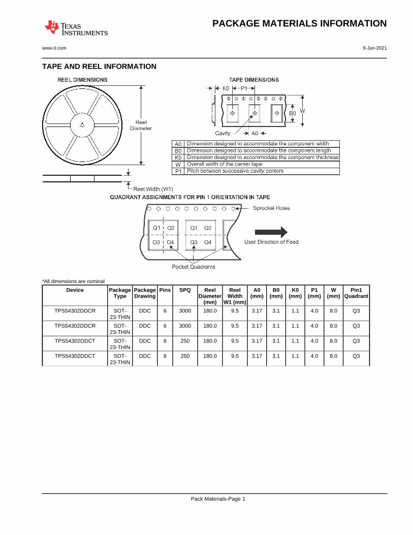
TAPE AND REEL INFORMATION
*All dimensions are nominal
Device PackageType
PackageDrawing
Pins SPQ ReelDiameter
(mm)
ReelWidth
W1 (mm)
A0(mm)
B0(mm)
K0(mm)
P1(mm)
W(mm)
Pin1Quadrant
TPS54302DDCR SOT-23-THIN
DDC 6 3000 180.0 9.5 3.17 3.1 1.1 4.0 8.0 Q3
TPS54302DDCR SOT-23-THIN
DDC 6 3000 180.0 9.5 3.17 3.1 1.1 4.0 8.0 Q3
TPS54302DDCT SOT-23-THIN
DDC 6 250 180.0 9.5 3.17 3.1 1.1 4.0 8.0 Q3
TPS54302DDCT SOT-23-THIN
DDC 6 250 180.0 9.5 3.17 3.1 1.1 4.0 8.0 Q3
PACKAGE MATERIALS INFORMATION
www.ti.com 9-Jun-2021
Pack Materials-Page 1
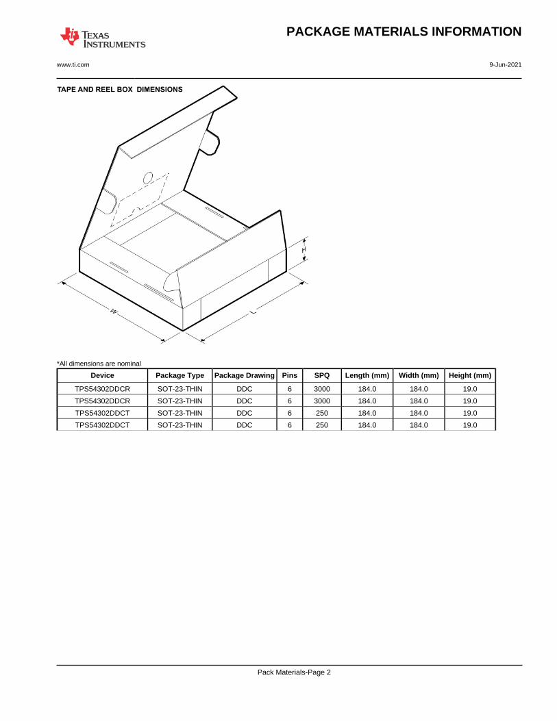
*All dimensions are nominal
Device Package Type Package Drawing Pins SPQ Length (mm) Width (mm) Height (mm)
TPS54302DDCR SOT-23-THIN DDC 6 3000 184.0 184.0 19.0
TPS54302DDCR SOT-23-THIN DDC 6 3000 184.0 184.0 19.0
TPS54302DDCT SOT-23-THIN DDC 6 250 184.0 184.0 19.0
TPS54302DDCT SOT-23-THIN DDC 6 250 184.0 184.0 19.0
PACKAGE MATERIALS INFORMATION
www.ti.com 9-Jun-2021
Pack Materials-Page 2
www.ti.com
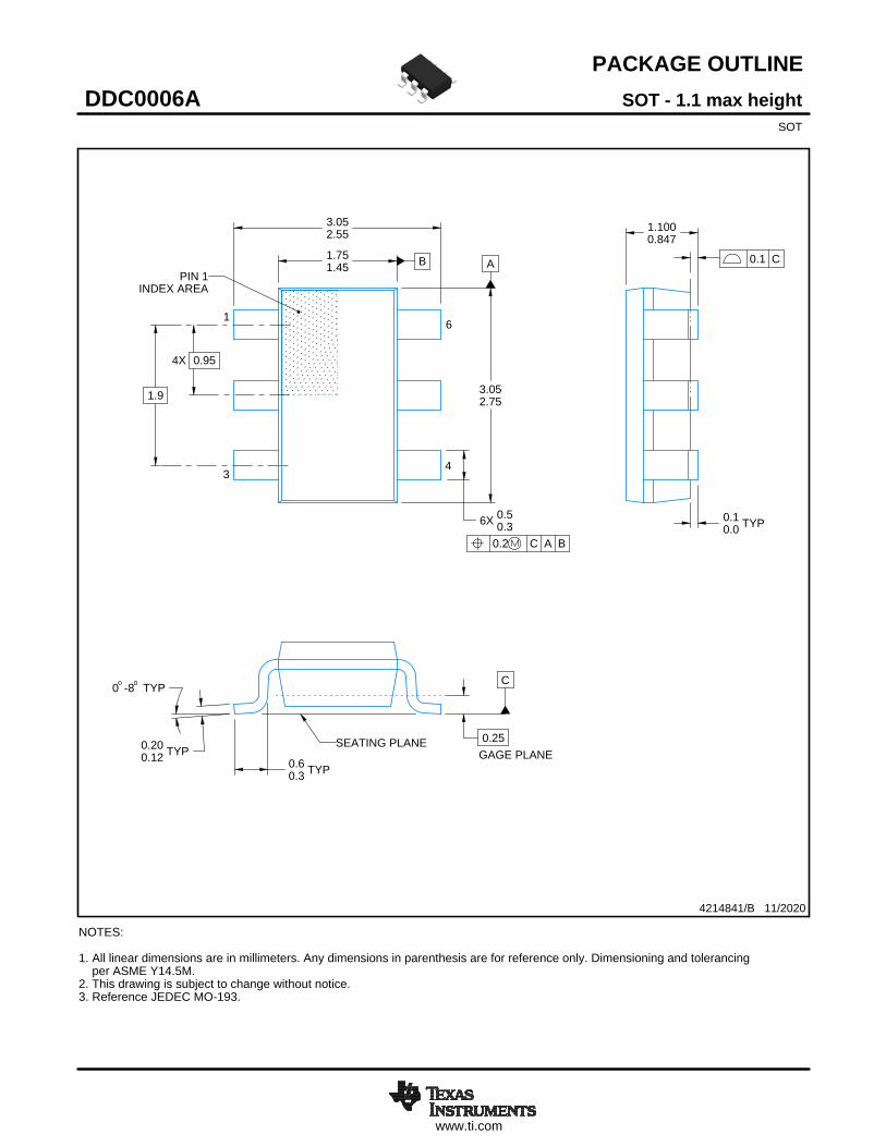
PACKAGE OUTLINE
C
0.200.12 TYP
0.25
3.052.55
4X 0.95
1.1000.847
0.10.0 TYP6X 0.5
0.3
0.60.3 TYP
1.9
0 -8 TYP
A
3.052.75
B1.751.45
SOT - 1.1 max heightDDC0006ASOT
4214841/B 11/2020
NOTES: 1. All linear dimensions are in millimeters. Any dimensions in parenthesis are for reference only. Dimensioning and tolerancing per ASME Y14.5M.2. This drawing is subject to change without notice.3. Reference JEDEC MO-193.
34
0.2 C A B
1 6
INDEX AREAPIN 1
GAGE PLANESEATING PLANE
0.1 C
SCALE 4.000
www.ti.com
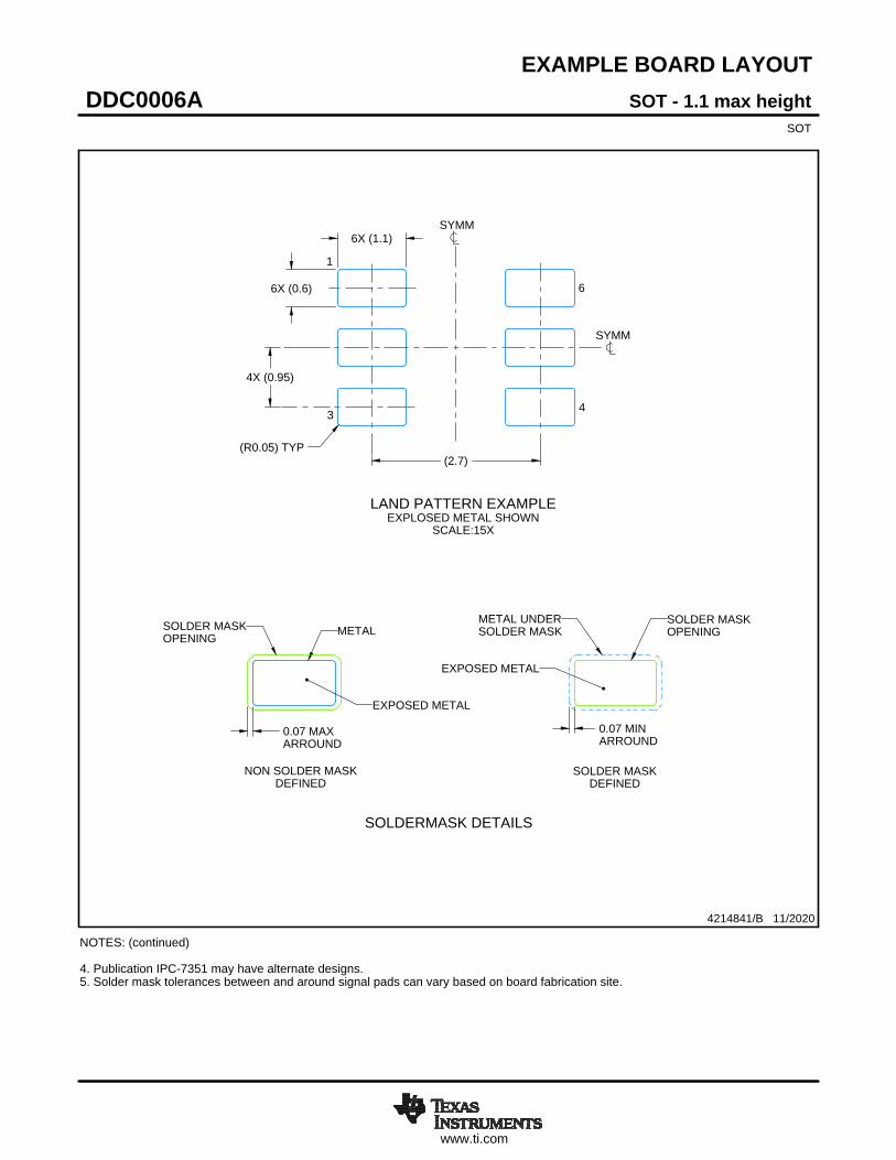
EXAMPLE BOARD LAYOUT
0.07 MAXARROUND
0.07 MINARROUND
6X (1.1)
6X (0.6)
(2.7)
4X (0.95)
(R0.05) TYP
4214841/B 11/2020
SOT - 1.1 max heightDDC0006ASOT
NOTES: (continued) 4. Publication IPC-7351 may have alternate designs. 5. Solder mask tolerances between and around signal pads can vary based on board fabrication site.
SYMM
LAND PATTERN EXAMPLEEXPLOSED METAL SHOWN
SCALE:15X
SYMM
1
3 4
6
SOLDER MASKOPENING
METAL UNDERSOLDER MASK
SOLDER MASKDEFINED
EXPOSED METAL
METALSOLDER MASKOPENING
NON SOLDER MASKDEFINED
SOLDERMASK DETAILS
EXPOSED METAL
www.ti.com
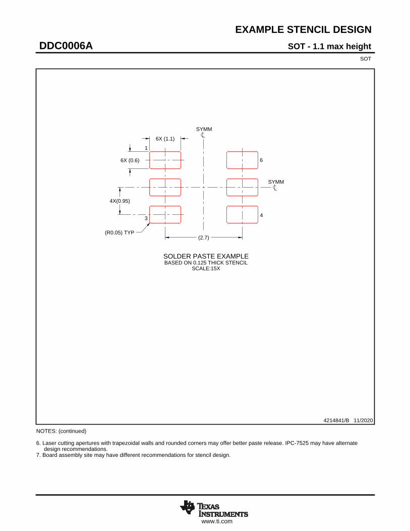
EXAMPLE STENCIL DESIGN
(2.7)
4X(0.95)
6X (1.1)
6X (0.6)
(R0.05) TYP
SOT - 1.1 max heightDDC0006ASOT
4214841/B 11/2020
NOTES: (continued) 6. Laser cutting apertures with trapezoidal walls and rounded corners may offer better paste release. IPC-7525 may have alternate design recommendations. 7. Board assembly site may have different recommendations for stencil design.
SOLDER PASTE EXAMPLEBASED ON 0.125 THICK STENCIL
SCALE:15X
SYMM
SYMM
1
3 4
6
IMPORTANT NOTICE AND DISCLAIMERTI PROVIDES TECHNICAL AND RELIABILITY DATA (INCLUDING DATASHEETS), DESIGN RESOURCES (INCLUDING REFERENCEDESIGNS), APPLICATION OR OTHER DESIGN ADVICE, WEB TOOLS, SAFETY INFORMATION, AND OTHER RESOURCES “AS IS”AND WITH ALL FAULTS, AND DISCLAIMS ALL WARRANTIES, EXPRESS AND IMPLIED, INCLUDING WITHOUT LIMITATION ANYIMPLIED WARRANTIES OF MERCHANTABILITY, FITNESS FOR A PARTICULAR PURPOSE OR NON-INFRINGEMENT OF THIRDPARTY INTELLECTUAL PROPERTY RIGHTS.These resources are intended for skilled developers designing with TI products. You are solely responsible for (1) selecting the appropriateTI products for your application, (2) designing, validating and testing your application, and (3) ensuring your application meets applicablestandards, and any other safety, security, or other requirements. These resources are subject to change without notice. TI grants youpermission to use these resources only for development of an application that uses the TI products described in the resource. Otherreproduction and display of these resources is prohibited. No license is granted to any other TI intellectual property right or to any third partyintellectual property right. TI disclaims responsibility for, and you will fully indemnify TI and its representatives against, any claims, damages,costs, losses, and liabilities arising out of your use of these resources.TI’s products are provided subject to TI’s Terms of Sale (https:www.ti.com/legal/termsofsale.html) or other applicable terms available eitheron ti.com or provided in conjunction with such TI products. TI’s provision of these resources does not expand or otherwise alter TI’sapplicable warranties or warranty disclaimers for TI products.IMPORTANT NOTICE
Mailing Address: Texas Instruments, Post Office Box 655303, Dallas, Texas 75265Copyright © 2021, Texas Instruments Incorporated
Top Related