


γλώσσες
Σελίδες
Νομικός


Microstrip Antennas
Prof. Girish KumarElectrical Engineering Department, IIT Bombay
(022) 2576 7436
Rectangular Microstrip Antenna (RMSA)
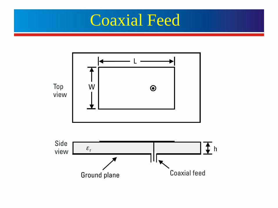
Co-axial feed
Side
Viewr
Ground plane
h
Top
View
L
W X
Y
x
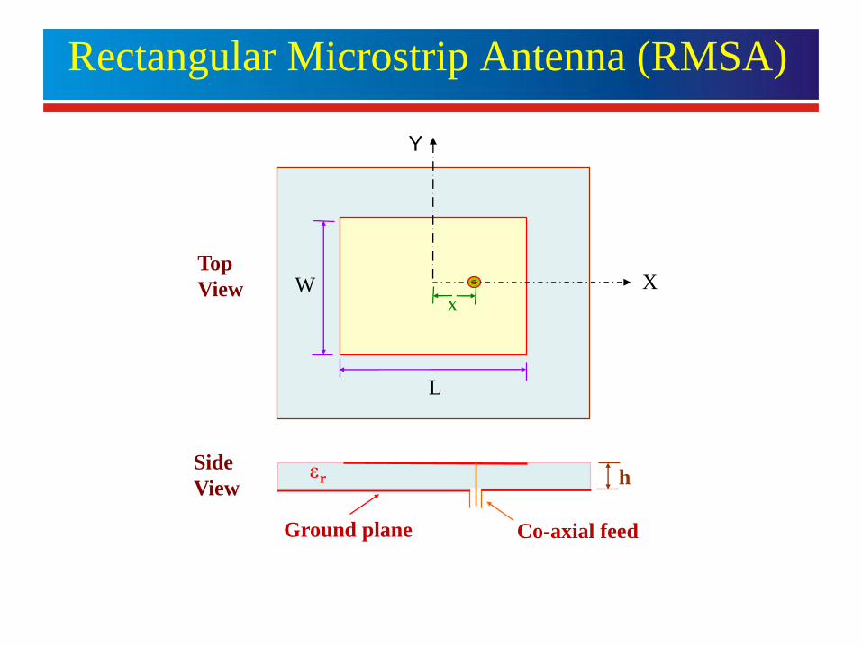
Microwave Integrated Circuits (MIC) vs MSA
Parameters MIC MSA
Dielectric
Constant (εr)
Large Small
Thickness (h) Small Large
Width (W) Generally Small
(impedance dependent)
Generally Large
Radiation Minimum (small fringing
fields)
Maximum (large
fringing fields)
Examples Filters, power dividers,
couplers, amplifiers, etc.
Antennas
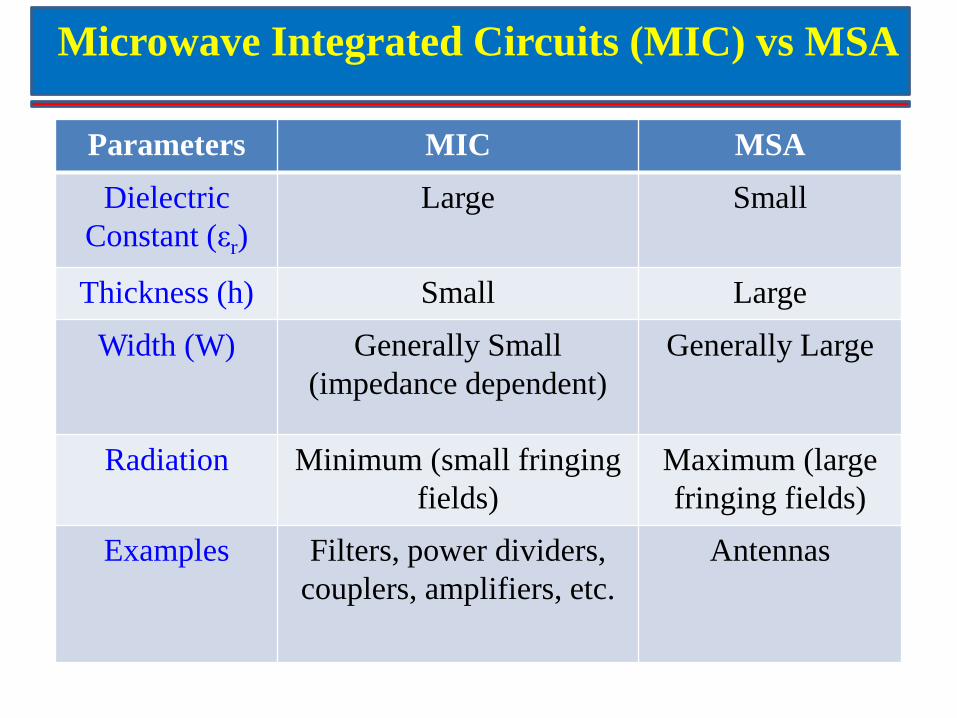
Substrates for MSA
Substrate Dielectric
Constant (εr)
Loss tangent
(tanδ)
Cost
Alumina 9.8 0.001 Very
High
Glass Epoxy 4.4 0.02 Low
Duroid /
Arlon
2.2 0.0009 Very
High
Foam 1.05 0.0001 Low/
Medium
Air 1 0 NA
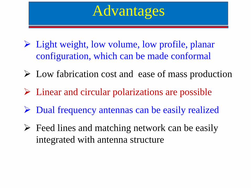
Advantages
Light weight, low volume, low profile, planar
configuration, which can be made conformal
Low fabrication cost and ease of mass production
Linear and circular polarizations are possible
Dual frequency antennas can be easily realized
Feed lines and matching network can be easily
integrated with antenna structure
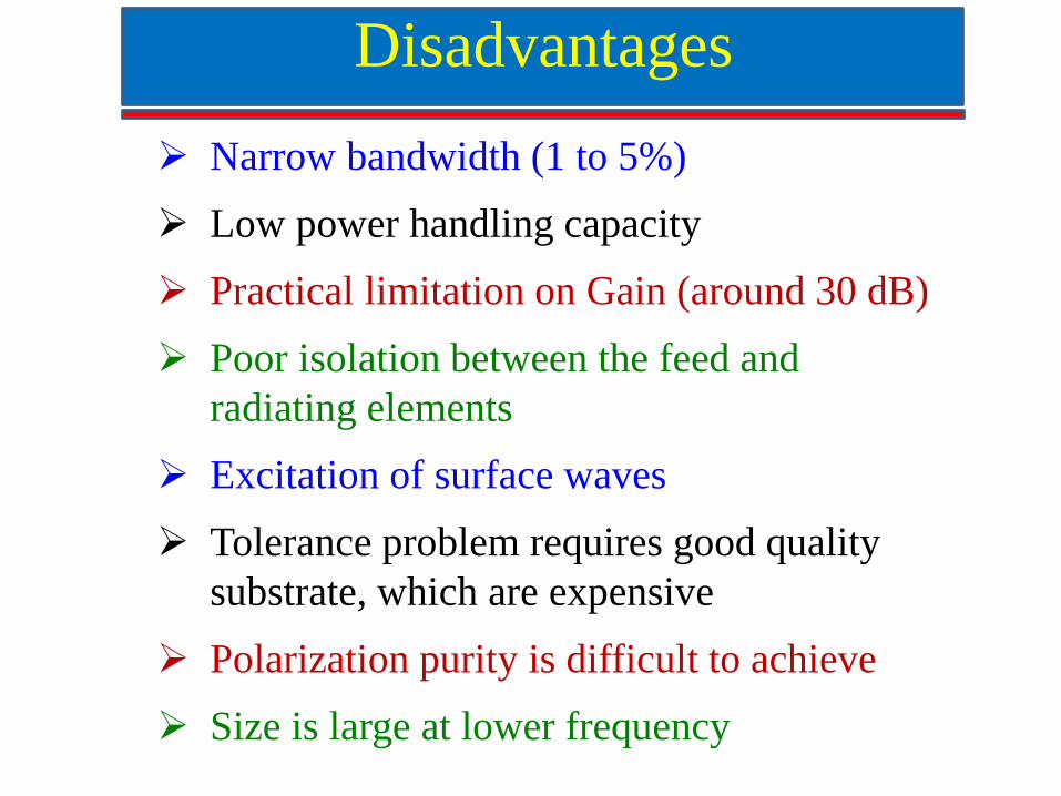
Disadvantages
Narrow bandwidth (1 to 5%)
Low power handling capacity
Practical limitation on Gain (around 30 dB)
Poor isolation between the feed and
radiating elements
Excitation of surface waves
Tolerance problem requires good quality
substrate, which are expensive
Polarization purity is difficult to achieve
Size is large at lower frequency
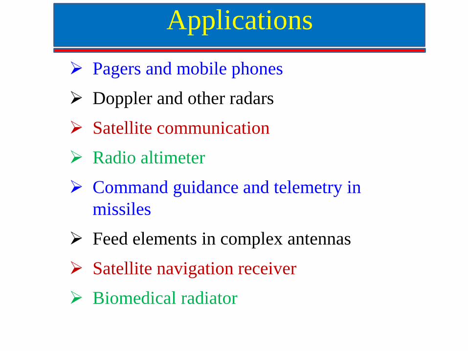
Applications
Pagers and mobile phones
Doppler and other radars
Satellite communication
Radio altimeter
Command guidance and telemetry in
missiles
Feed elements in complex antennas
Satellite navigation receiver
Biomedical radiator
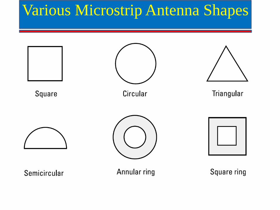
Various Microstrip Antenna Shapes

MSA Feeding Techniques
Coaxial Feed
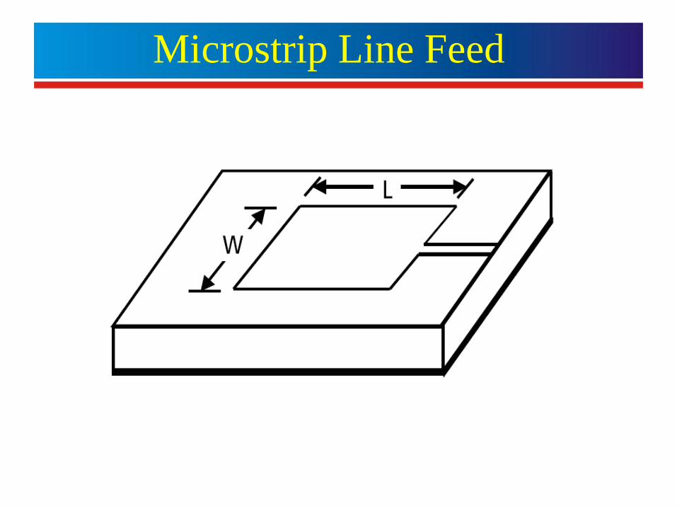
Microstrip Line Feed
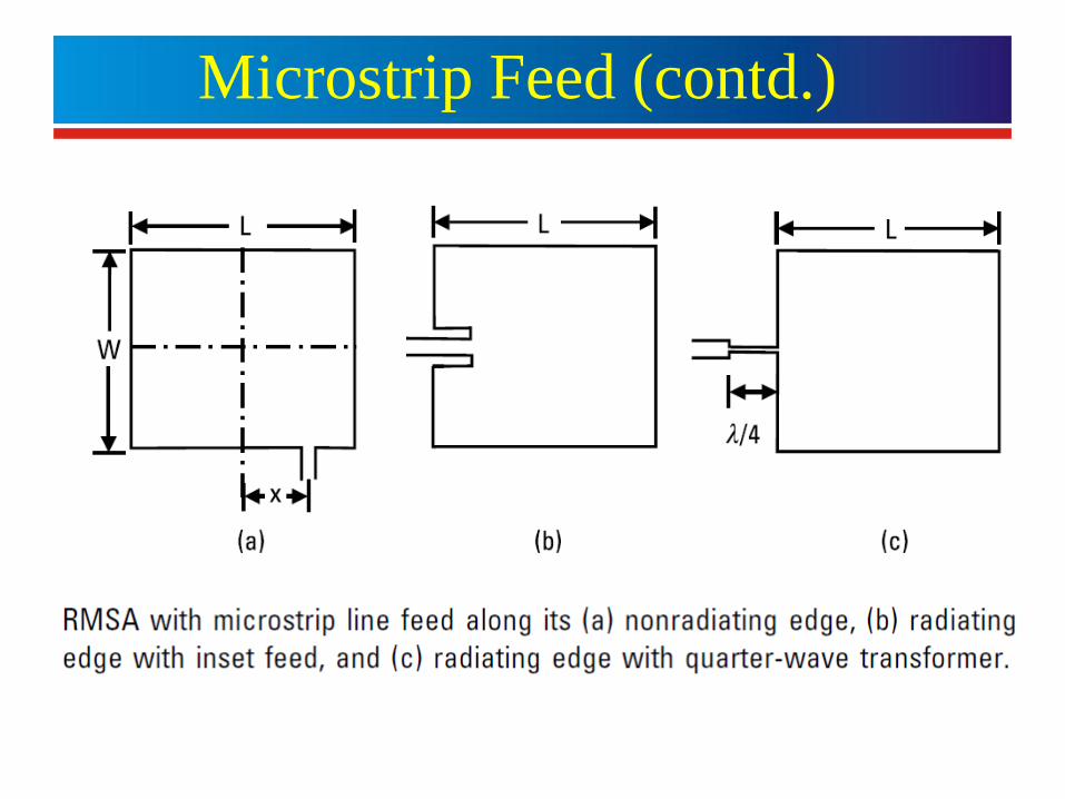
Microstrip Feed (contd.)
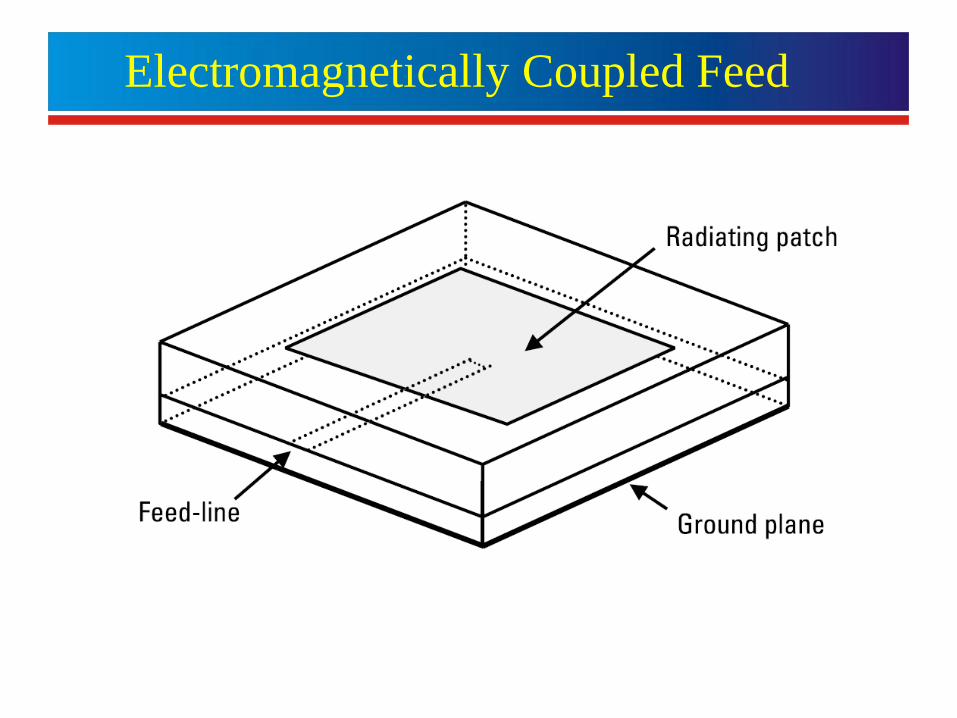
Electromagnetically Coupled Feed
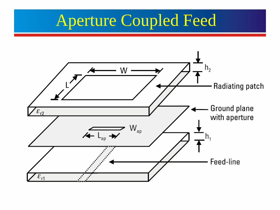
Aperture Coupled Feed
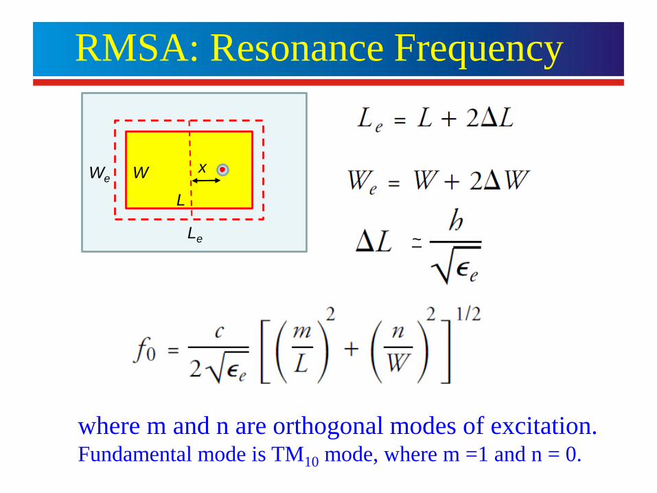
RMSA: Resonance Frequency
where m and n are orthogonal modes of excitation. Fundamental mode is TM10 mode, where m =1 and n = 0.
L
Le
W We
~
x
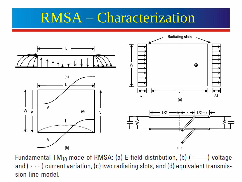
RMSA – Characterization

RMSA: Design Equations
Smaller or larger W can be taken than
the W obtained from this expression.
BW α W and Gain α W
Choose feed-point x between L/6 to L/4.
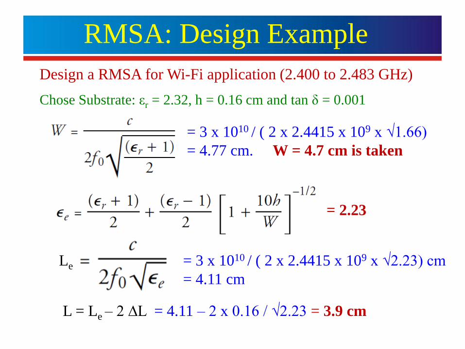
RMSA: Design Example
Design a RMSA for Wi-Fi application (2.400 to 2.483 GHz)
Chose Substrate: εr = 2.32, h = 0.16 cm and tan δ = 0.001
= 3 x 10¹⁰ / ( 2 x 2.4415 x 109 x √1.66)
= 4.77 cm. W = 4.7 cm is taken
= 2.23
Le = 3 x 10¹⁰ / ( 2 x 2.4415 x 109 x √2.23) cm
= 4.11 cm
L = Le – 2 ∆L = 4.11 – 2 x 0.16 / √2.23 = 3.9 cm
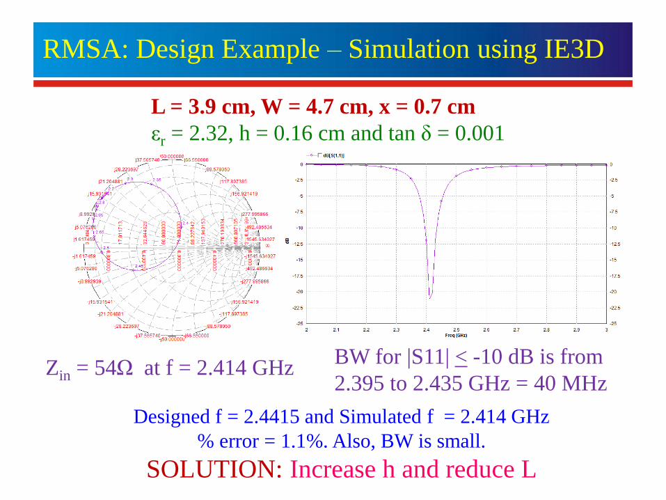
RMSA: Design Example – Simulation using IE3D
L = 3.9 cm, W = 4.7 cm, x = 0.7 cm
εr = 2.32, h = 0.16 cm and tan δ = 0.001
Zin = 54Ω at f = 2.414 GHzBW for |S11| < -10 dB is from
2.395 to 2.435 GHz = 40 MHz
Designed f = 2.4415 and Simulated f = 2.414 GHz
% error = 1.1%. Also, BW is small.
SOLUTION: Increase h and reduce L
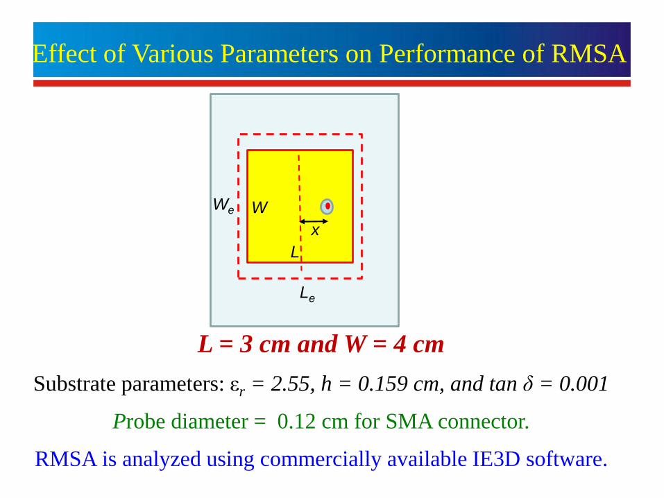
L = 3 cm and W = 4 cm
Substrate parameters: εr = 2.55, h = 0.159 cm, and tan δ = 0.001
Probe diameter = 0.12 cm for SMA connector.
RMSA is analyzed using commercially available IE3D software.
Effect of Various Parameters on Performance of RMSA
L
Le
W We
x
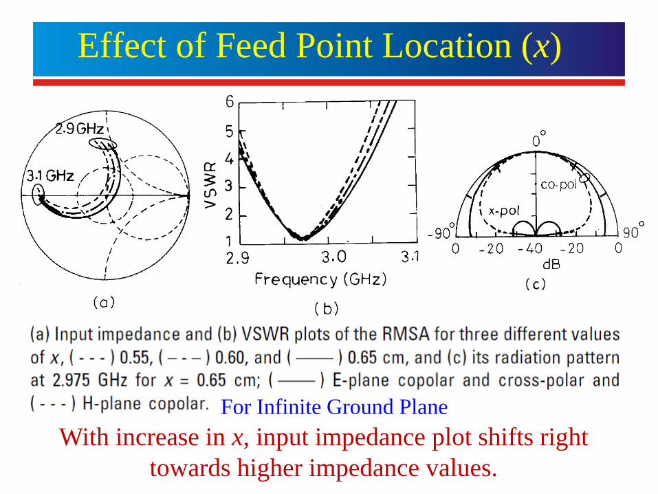
Effect of Feed Point Location (x)
For Infinite Ground Plane
With increase in x, input impedance plot shifts right
towards higher impedance values.
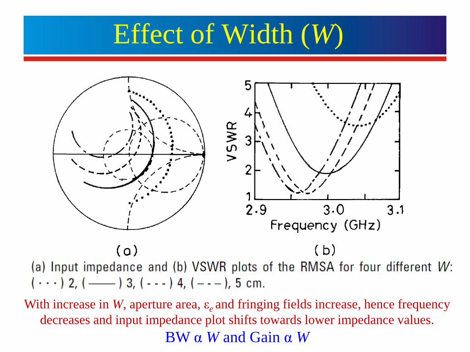
Effect of Width (W)
With increase in W, aperture area, εe and fringing fields increase, hence frequency
decreases and input impedance plot shifts towards lower impedance values.
BW α W and Gain α W
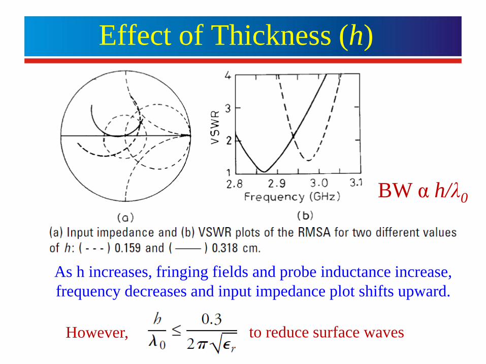
Effect of Thickness (h)
However, to reduce surface waves
As h increases, fringing fields and probe inductance increase,
frequency decreases and input impedance plot shifts upward.
BW α h/λ0
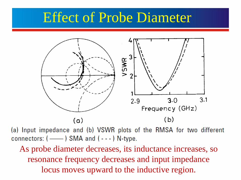
Effect of Probe Diameter
As probe diameter decreases, its inductance increases, so
resonance frequency decreases and input impedance
locus moves upward to the inductive region.
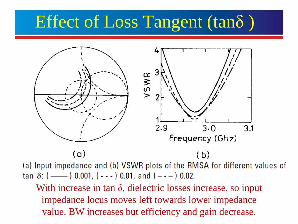
Effect of Loss Tangent (tanδ )
With increase in tan δ, dielectric losses increase, so input
impedance locus moves left towards lower impedance
value. BW increases but efficiency and gain decrease.
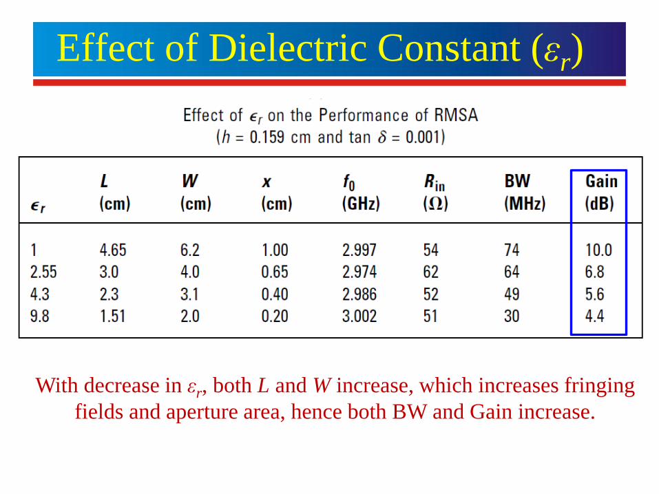
Effect of Dielectric Constant (εr)
With decrease in εr, both L and W increase, which increases fringing
fields and aperture area, hence both BW and Gain increase.
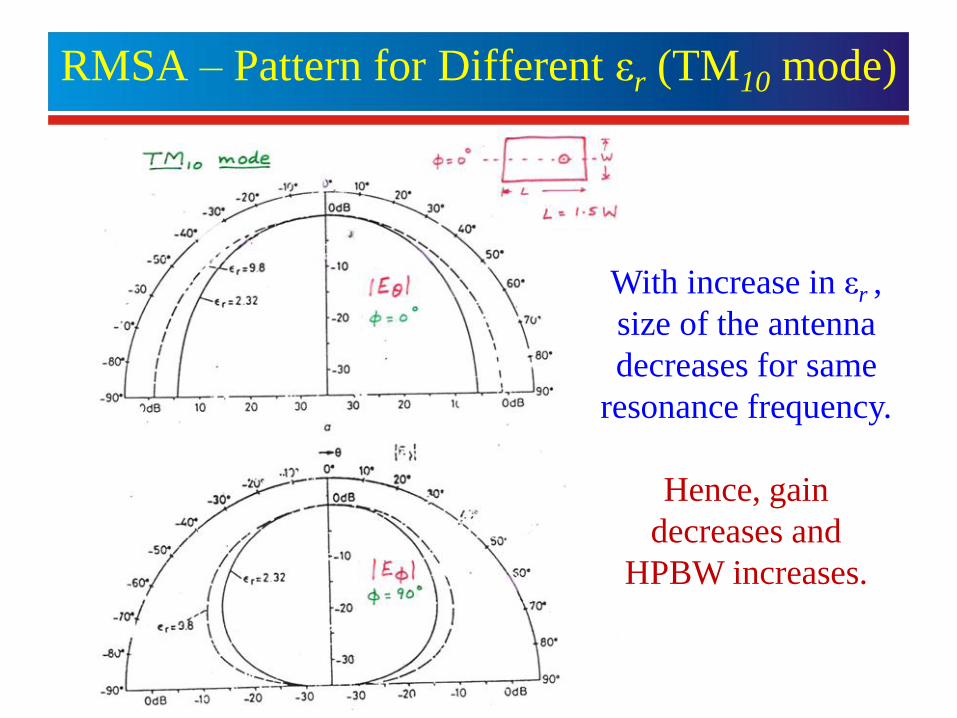
RMSA – Pattern for Different εr (TM10 mode)
With increase in εr ,
size of the antenna
decreases for same
resonance frequency.
Hence, gain
decreases and
HPBW increases.
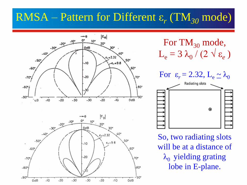
RMSA – Pattern for Different εr (TM30 mode)
For TM30 mode,
Le = 3 λ0 / (2 √ εe )
For εr = 2.32, Le ~ λ0
So, two radiating slots
will be at a distance of
λ0 yielding grating
lobe in E-plane.
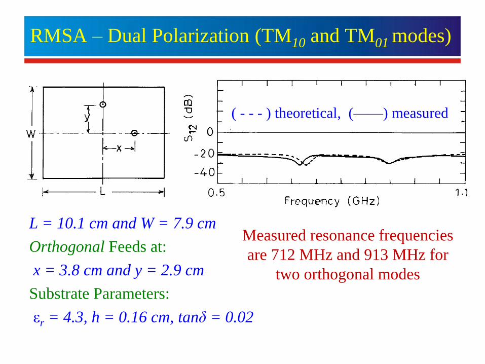
RMSA – Dual Polarization (TM10 and TM01 modes)
L = 10.1 cm and W = 7.9 cm
Orthogonal Feeds at:
x = 3.8 cm and y = 2.9 cm
Substrate Parameters:
εr = 4.3, h = 0.16 cm, tanδ = 0.02
( - - - ) theoretical, (——) measured
Measured resonance frequencies
are 712 MHz and 913 MHz for
two orthogonal modes
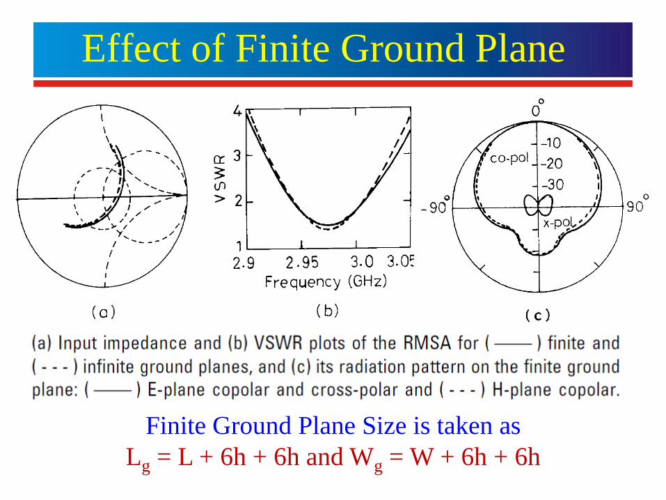
Effect of Finite Ground Plane
Finite Ground Plane Size is taken as
Lg = L + 6h + 6h and Wg = W + 6h + 6h
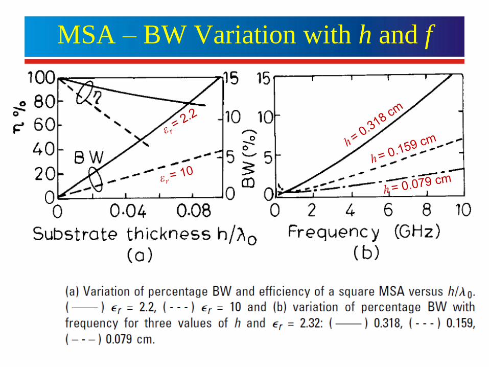
MSA – BW Variation with h and f
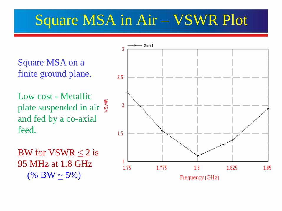
Square MSA in Air – VSWR Plot
Square MSA on a
finite ground plane.
Low cost - Metallic
plate suspended in air
and fed by a co-axial
feed.
BW for VSWR < 2 is
95 MHz at 1.8 GHz
(% BW ~ 5%)
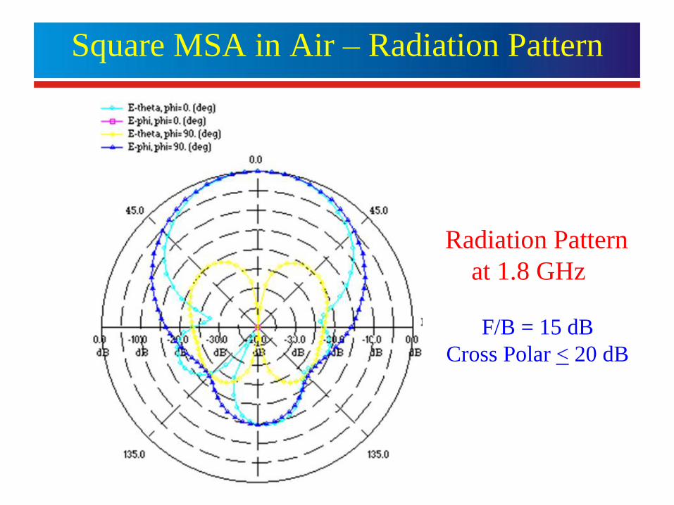
Square MSA in Air – Radiation Pattern
Radiation Pattern
at 1.8 GHz
F/B = 15 dB
Cross Polar < 20 dB
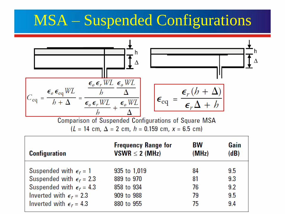
MSA – Suspended Configurations
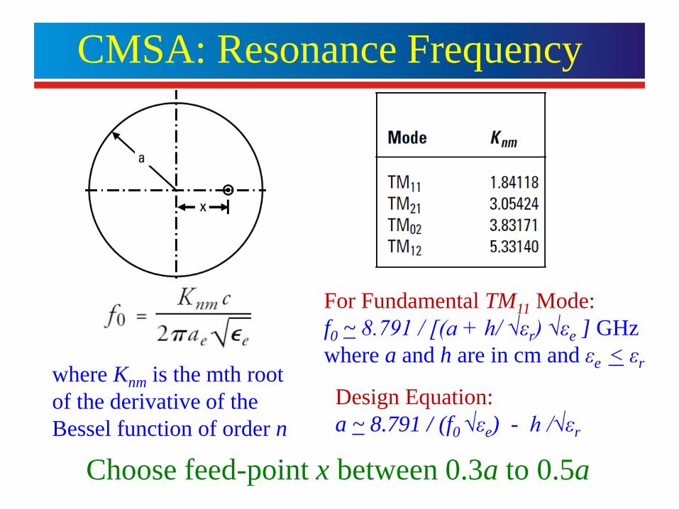
CMSA: Resonance Frequency
where Knm is the mth root
of the derivative of the
Bessel function of order n
For Fundamental TM11 Mode:
f0 ~ 8.791 / [(a + h/ √εr) √εe ] GHz
where a and h are in cm and εe < εr
Design Equation:
a ~ 8.791 / (f0 √εe) - h /√εr
Choose feed-point x between 0.3a to 0.5a
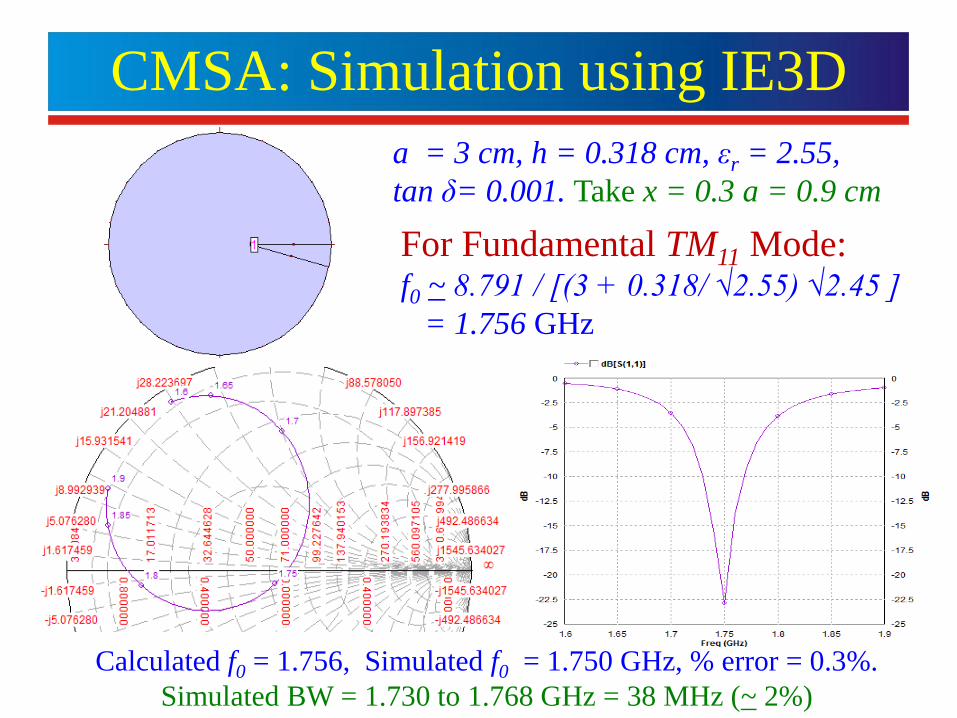
CMSA: Simulation using IE3D
For Fundamental TM11 Mode:f0 ~ 8.791 / [(3 + 0.318/ √2.55) √2.45 ]
= 1.756 GHz
a = 3 cm, h = 0.318 cm, εr = 2.55,
tan δ= 0.001. Take x = 0.3 a = 0.9 cm
Calculated f0 = 1.756, Simulated f0 = 1.750 GHz, % error = 0.3%.
Simulated BW = 1.730 to 1.768 GHz = 38 MHz (~ 2%)
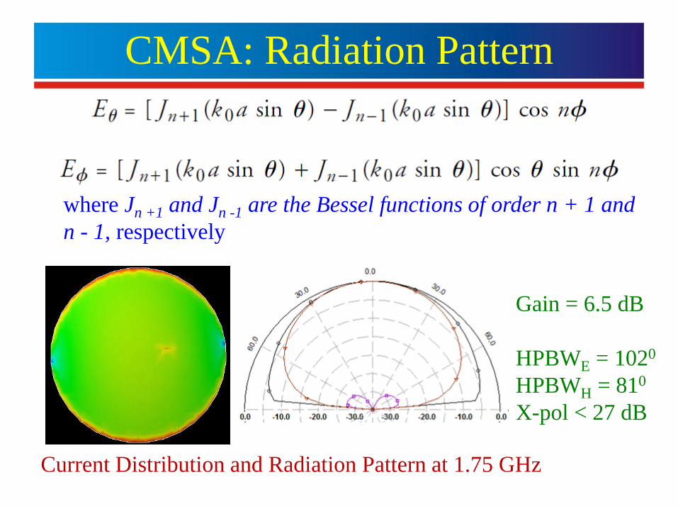
CMSA: Radiation Pattern
where Jn +1 and Jn -1 are the Bessel functions of order n + 1 and
n - 1, respectively
Current Distribution and Radiation Pattern at 1.75 GHz
Gain = 6.5 dB
HPBWE = 1020
HPBWH = 810
X-pol < 27 dB
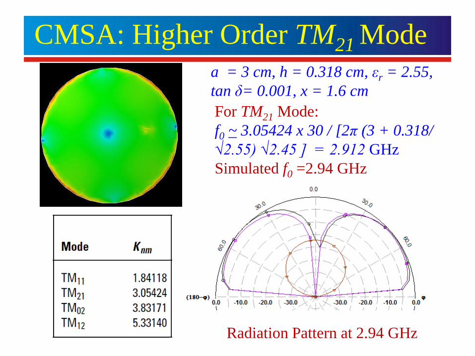
CMSA: Higher Order TM21 Mode
For TM21 Mode:
f0 ~ 3.05424 x 30 / [2π (3 + 0.318/
√2.55) √2.45 ] = 2.912 GHz
Simulated f0 =2.94 GHz
a = 3 cm, h = 0.318 cm, εr = 2.55,
tan δ= 0.001, x = 1.6 cm
Radiation Pattern at 2.94 GHz
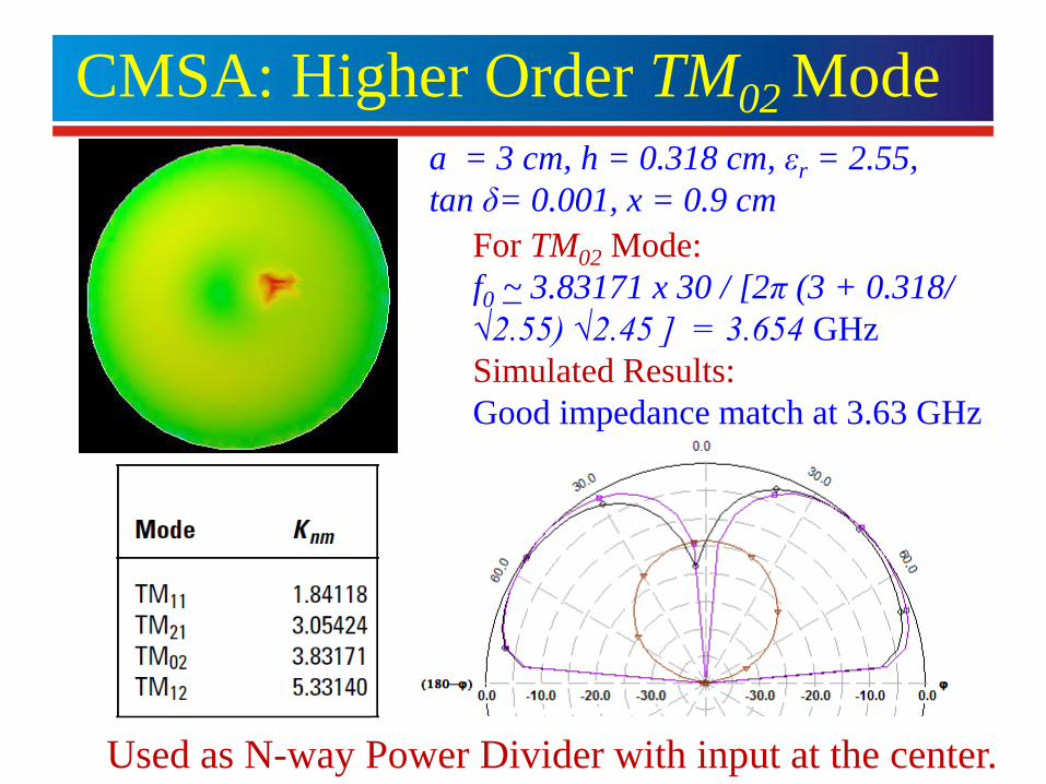
CMSA: Higher Order TM02 Mode
For TM02 Mode:
f0 ~ 3.83171 x 30 / [2π (3 + 0.318/
√2.55) √2.45 ] = 3.654 GHz
Simulated Results:
Good impedance match at 3.63 GHz
a = 3 cm, h = 0.318 cm, εr = 2.55,
tan δ= 0.001, x = 0.9 cm
Used as N-way Power Divider with input at the center.
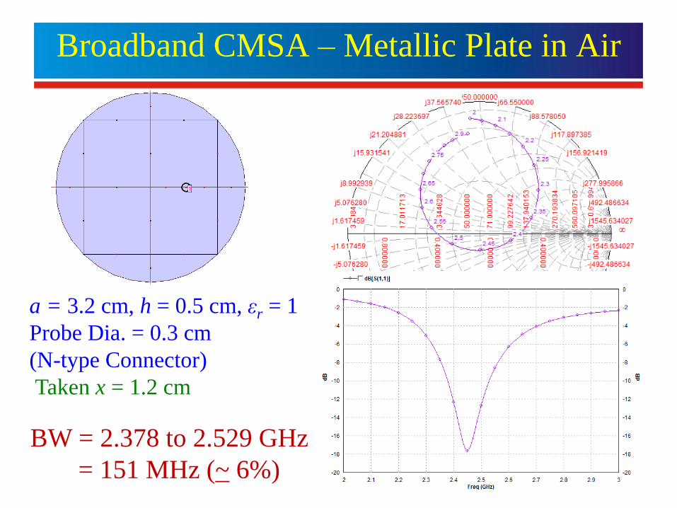
Broadband CMSA – Metallic Plate in Air
a = 3.2 cm, h = 0.5 cm, εr = 1
Probe Dia. = 0.3 cm
(N-type Connector)
Taken x = 1.2 cm
BW = 2.378 to 2.529 GHz
= 151 MHz (~ 6%)
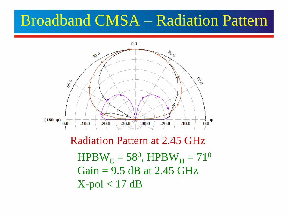
Broadband CMSA – Radiation Pattern
HPBWE = 580, HPBWH = 710
Gain = 9.5 dB at 2.45 GHz
X-pol < 17 dB
Radiation Pattern at 2.45 GHz
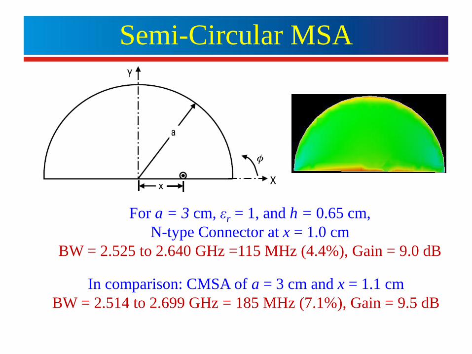
Semi-Circular MSA
For a = 3 cm, εr = 1, and h = 0.65 cm,
N-type Connector at x = 1.0 cm
BW = 2.525 to 2.640 GHz =115 MHz (4.4%), Gain = 9.0 dB
In comparison: CMSA of a = 3 cm and x = 1.1 cm
BW = 2.514 to 2.699 GHz = 185 MHz (7.1%), Gain = 9.5 dB
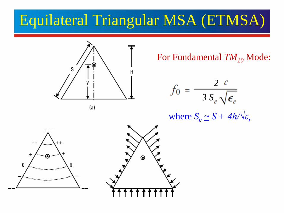
Equilateral Triangular MSA (ETMSA)
2
3 S
where Se ~ S + 4h/√εr
For Fundamental TM10 Mode:
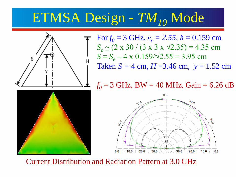
ETMSA Design - TM10 Mode
For f0 = 3 GHz, εr = 2.55, h = 0.159 cm
Se ~ (2 x 30 / (3 x 3 x √2.35) = 4.35 cm
S = Se – 4 x 0.159/√2.55 = 3.95 cm
Taken S = 4 cm, H =3.46 cm, y = 1.52 cm
f0 = 3 GHz, BW = 40 MHz, Gain = 6.26 dB
Current Distribution and Radiation Pattern at 3.0 GHz
Top Related