


γλώσσες
Σελίδες
Νομικός

Organic Substrate - LCP
• Liquid Crystal Polymer (LCP) can be used as a high performance multilayer substrate
• Excellent electrical properties (εr ~ 3.10 and tanδ=0.002)
• Flexible (printed circuits can be rolled or molded into desired shape)
• Good performance: mechanical integration compatibility and economic viability
Wideband (9%) UHF RFID tag on LCP to cover the global 860-930 MHz band
Antennas fabricated on 12”x12” in LCP Film
Why consider LCP as a substrate?
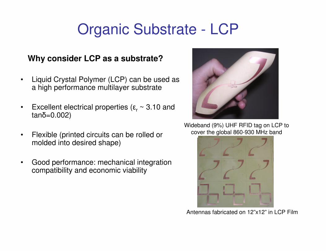
Why Consider Paper as a Substrate?
- Environmental Friendly and low cost (LOWEST COST MATERIAL MADE BY HUMANKIND)
- Large Reel to Reel Processing
- Low surface profile with appropriate coating
- Compatible for printing circuitry by direct write methodologies
- Host nano-scale additives (e.g. fire retardant textiles)
- Can be made hydrophobic
- Dielectric constant εr (~3) close to air’s, allowing EM waves to penetrate substrate easily with minimum (5-6%) power reflection
Coated paper
Drop of water on hydrophobic paper
Organic Substrate - Paper
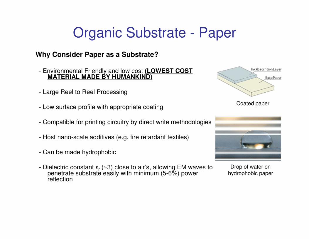
The down shifted TEmnp mode resonant frequency between an empty and a lorded cavity gives the information of the sample dielectric constant.
Empty Cylinder (unloaded)
peak shifting
Paper Sample Inserted (loaded)
TE011 ∆f=2.2%
Paper Dielectric Properties Characterization
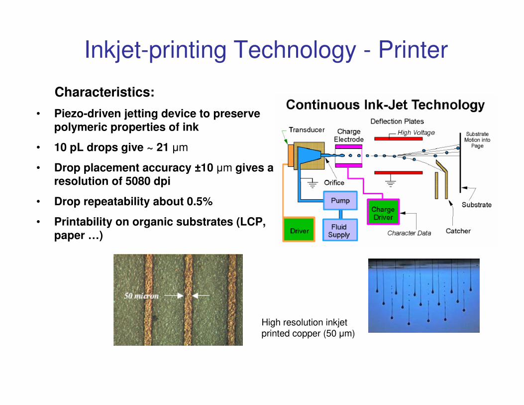
Characteristics:
• Piezo-driven jetting device to preserve polymeric properties of ink
• 10 pL drops give ~ 21 µm
• Drop placement accuracy ±10 µm gives a resolution of 5080 dpi
• Drop repeatability about 0.5%
• Printability on organic substrates (LCP, paper …)
Inkjet-printing Technology - Printer
High resolution inkjet printed copper (50 µm)
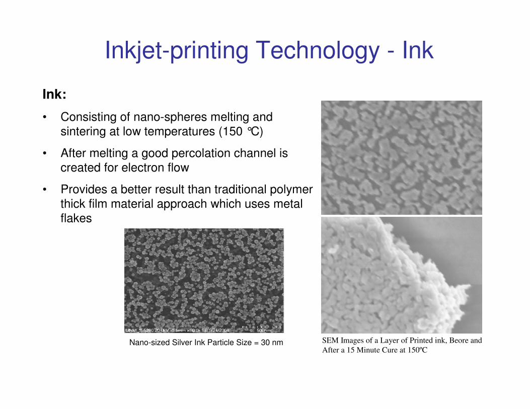
Nano-sized Silver Ink Particle Size = 30 nm SEM Images of a Layer of Printed ink, Beore and
After a 15 Minute Cure at 150ºC
Ink:
• Consisting of nano-spheres melting and sintering at low temperatures (150 °C)
• After melting a good percolation channel is created for electron flow
• Provides a better result than traditional polymer thick film material approach which uses metal flakes
Inkjet-printing Technology - Ink
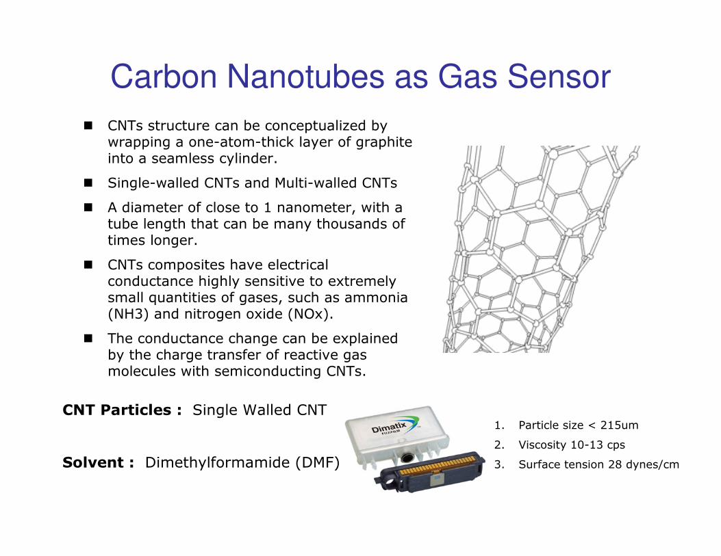
Carbon Nanotubes as Gas Sensor
� CNTs structure can be conceptualized by wrapping a one-atom-thick layer of graphite into a seamless cylinder.
� Single-walled CNTs and Multi-walled CNTs
� A diameter of close to 1 nanometer, with a tube length that can be many thousands of times longer.
� CNTs composites have electrical conductance highly sensitive to extremely small quantities of gases, such as ammonia (NH3) and nitrogen oxide (NOx).
� The conductance change can be explained by the charge transfer of reactive gas molecules with semiconducting CNTs.
CNT Particles : Single Walled CNT
Solvent : Dimethylformamide (DMF)
1. Particle size < 215um
2. Viscosity 10-13 cps
3. Surface tension 28 dynes/cm
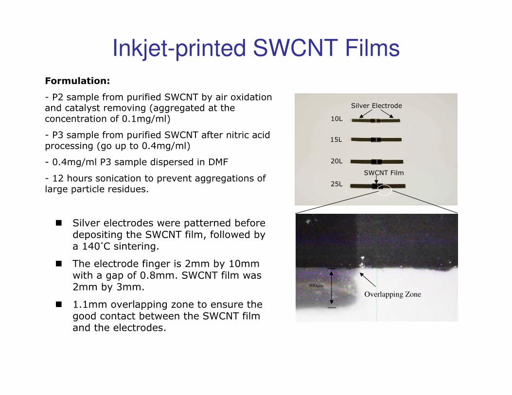
Inkjet-printed SWCNT Films
Overlapping Zone
500um
10L
15L
20L
25L
SWCNT Film
Silver Electrode
� Silver electrodes were patterned before depositing the SWCNT film, followed by a 140˚C sintering.
� The electrode finger is 2mm by 10mm with a gap of 0.8mm. SWCNT film was 2mm by 3mm.
� 1.1mm overlapping zone to ensure the good contact between the SWCNT film and the electrodes.
Formulation:
- P2 sample from purified SWCNT by air oxidation and catalyst removing (aggregated at the concentration of 0.1mg/ml)
- P3 sample from purified SWCNT after nitric acid processing (go up to 0.4mg/ml)
- 0.4mg/ml P3 sample dispersed in DMF
- 12 hours sonication to prevent aggregations of large particle residues.
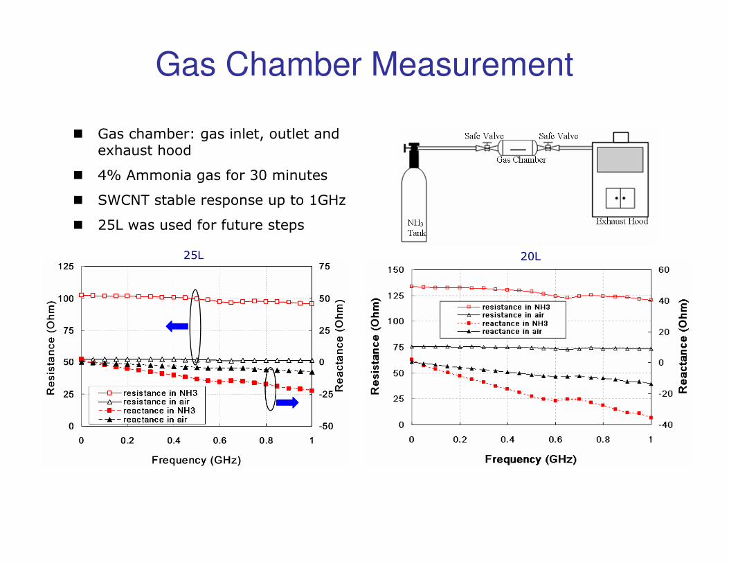
Gas Chamber Measurement
� Gas chamber: gas inlet, outlet and exhaust hood
� 4% Ammonia gas for 30 minutes
� SWCNT stable response up to 1GHz
� 25L was used for future steps
25L 20L
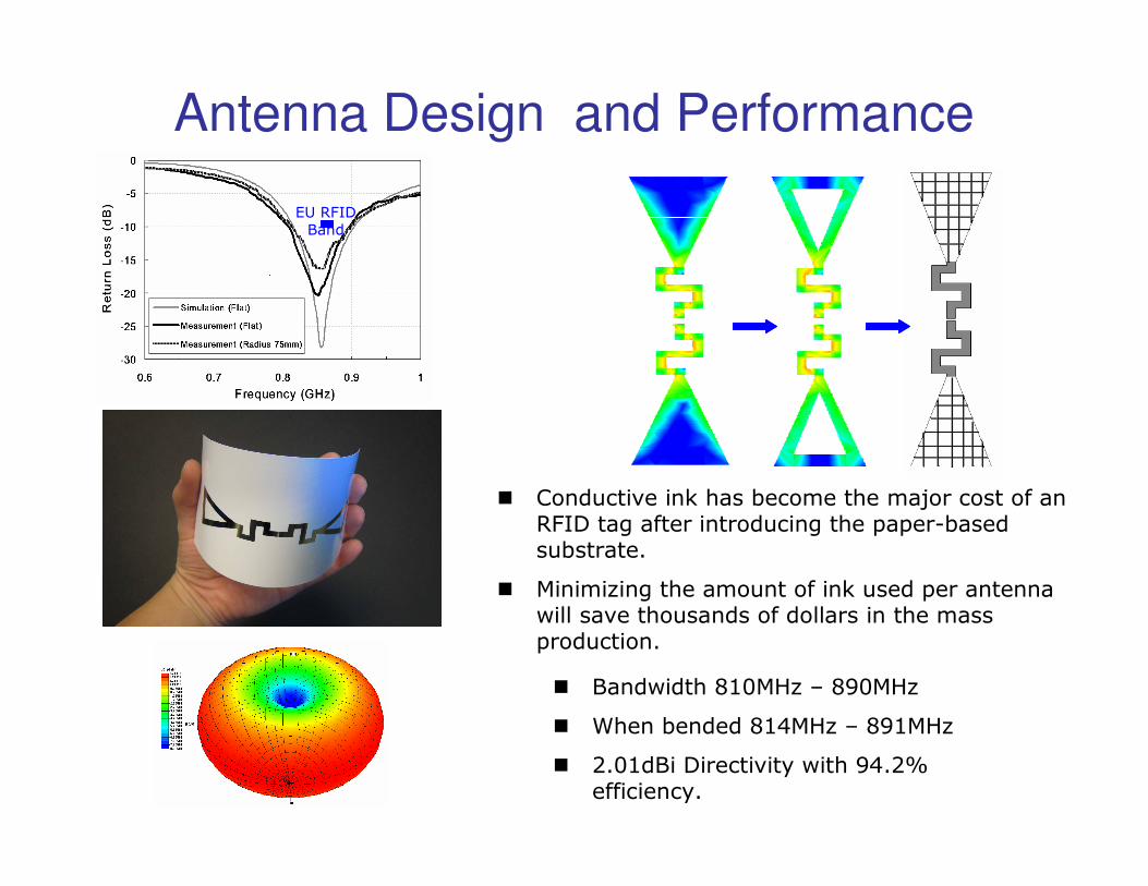
Antenna Design and Performance
EU RFID Band
� Bandwidth 810MHz – 890MHz
� When bended 814MHz – 891MHz
� 2.01dBi Directivity with 94.2% efficiency.
� Conductive ink has become the major cost of an RFID tag after introducing the paper-based substrate.
� Minimizing the amount of ink used per antenna will save thousands of dollars in the mass production.
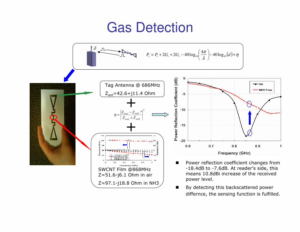
Gas Detection
( ) ηλ
π+−
−++= dGGPP
rttr 1010 log404
log4022
SWCNT Film @868MHz Z=51.6-j6.1 Ohm in air
Z=97.1-j18.8 Ohm in NH3
Tag Antenna @ 686MHz
Zant=42.6+j11.4 Ohm
2
*
ANTload
ANTIoad
ZZ
ZZ
+
−=η
+
+
� Power reflection coefficient changes from -18.4dB to -7.6dB. At reader’s side, this means 10.8dBi increase of the received power level.
� By detecting this backscattered power
differnce, the sensing function is fulfilled.
Top Related