


γλώσσες
Σελίδες
Νομικός

> REPLACE THIS LINE WITH YOUR PAPER IDENTIFICATION NUMBER (DOUBLE-CLICK HERE TO EDIT) <
1
Abstract— 40-Gb/s/λ multi-band carrierless amplitude and
phase (CAP) modulation long reach passive optical networks
(LR-PONs) were demonstrated using 10-G class transceivers only.
A major issue of multi-band CAP is that it is vulnerable to timing
error and this work has offered quantitative analysis about it in
detail for the first time. A novel simple timing recovery approach,
partial differential QAM constellation encoding and decoding
schemes together with blind multi-modulus algorithms (MMAs)
equalization are proposed to address the issue efficiently, enabling
zero-overhead signal recovery. Results show that it can offer
excellent system tolerance to timing error of at least ±0.1 symbol
period even for the highest frequency CAP sub-band. The
characteristics of the transceiver are measured and optimization
of critical system parameters is performed including the CAP
sub-band count, 10-G Mach-Zehnder intensity modulator
operation conditions, optical launch power, and wavelength offset
asymmetrical optical filtering. For downlink using erbium-doped
fiber amplifier (EDFA) pre-amplifiers, successful 40-Gb/s
multi-band CAP signal transmission over an 80-km (90-km) SMF
is achieved with a link power budget of 33 dB (29 dB) considering
a FEC threshold BER of 3.8×10⁻³ .
Index Terms—Long reach passive optical network, Carrierless
amplitude and phase modulation, Modulation format,
Multi-modulus algorithm, Partial differential QAM, Optical
power budget, Blind equalization, Timing error, Timing recovery,
phase ambiguity, cycle slip.
I. INTRODUCTION
lthough the industry is ready to deploy the fastest
standardized 40-Gb/s time and wavelength division
multiplexing passive optical networks (TWDM-PONs) [1], the
next generation (NG)-PONs beyond 40-Gb/s have been
intensively investigated featuring 25 Gb/s or 40 Gb/s lane rate
or beyond as a result of the continuous rise in broadband service
demand. For example, the IEEE 802.3 Ethernet Working Group
is discussing on 4 channels with 25 Gb/s lane rate as an option
Manuscript received ?, 2017; Revised 2017; Accepted ?, 2017.
Jinlong Wei is now with Huawei Technologies Duesseldorf GmbH,
European Research Center, Riesstrasse 25, 80992 München, Germany ([email protected]). He was with ADVA Optical Networking SE,
Märzenquelle 1-3, 98617 Meiningen, Germany.
Elias Giacoumidis is now with both the School of Electronic Engineering, Dublin City University, The Rince Institute, Dublin 9, Irland and the SFI
research center CONNECT, 34 Westland Row, Trinity College Dublin, Dublin
2, Ireland ([email protected]). Copyright (c) 2015 IEEE.
for NG-EPON [2]. This is mainly fueled by bandwidth-hungry
applications such as high definition TV and video-on-demand
as well as emerging services like virtual reality and cloud
computing. In addition, the 5G Infrastructure Public Private
Partnership (5G PPP) anticipates that 5G mobile networks need
to accommodate a 1000-fold increase in data traffic thus
low-cost mobile front-haul traffic will become one of the major
drivers for PON data rates exceeding 10 Gb/s [3,4]. Focus is on
low-cost solutions using advanced single carrier modulation
schemes and demonstrations have been performed including
chirp managed NRZ [5-7], electrical/optical Duobinary [8-10],
and PAM-4 [8,11]. These schemes have shown the feasibility
of supporting 25 Gb/s or 40 Gb/s data rate over typically 20-km
SMF using 10-G transmitter [7-11] and/or 10-G receiver [7-9],
thus are capable of offering low-cost solutions.
In addition to use of low cost optics, high speed long reach
PONs (LR-PONs) are key technologies to facilitate
metro/access and fixed-mobile convergences to further reduce
cost and power [12]. This is critcal for cost and power saving
from operators’ point of view. At high bit rates of 40 Gb/s/λ,
however, the above-mentioned single carrier schemes with
simple linear or nonlinear equalizations [10,11,13,14] are
difficult to support transmission beyond 20-km SMF with
reasonably high optical link power budgets unless dedicated
dispersion compensation fibers (DCFs) [8, 9] are adopted. The
use of DCFs increases system cost and insertion loss, reduces
system flexibility and complicates link configuration. On the
contrary, multi-carrier [15,16] and/or multi-band schemes
[17,18] featuring enhanced spectral efficiency and flexibility by
fully leveraging advanced digital signal process (DSP) can
support high capacity and long reach without altering the
optical infrastructure. In addition, simple asymmetrical optical
filtering by utilizing the deployed wavelength division
multiplexing (WDM) multiplexers (MUXs) and
de-multiplexers (De-MUXs) or Arrayed waveguide gratings
(AWGs) is advantageous for multi-band or multi-carrier
systems to increase fiber dispersion tolerance [16-18]. As
indicated in [7], such optical filtering approach can achieve
stable performance in field trial demonstrations.
High speed single- or multi-band carrierless amplitude and
phase (CAP) modulation systems have been intensively
investigated for a potential low cost solutions for medium and
long reach PONs [18-21]. Nevertheless, none of these
demonstrations except [19] paid much attention to the
Multi-Band CAP for Next Generation Optical
Access Networks Using 10-G Optics
(Invited Paper)
Jinlong Wei, Senior Member, IEEE, and Elias Giacoumidis, Member, IEEE
A
> REPLACE THIS LINE WITH YOUR PAPER IDENTIFICATION NUMBER (DOUBLE-CLICK HERE TO EDIT) <
2
significant technical issue of the strong sensitivity of CAP
signals to timing jitter. This is an intrinsic disadvantage for
CAP especially when multiple bands are implemented [22].
Although training symbols-assisted phase tracking and
estimation in the receiver side can recover the signal [18,21], it
introduces overhead and additionally high frequency non-data
dependent jitter beyond the phase tacking loop bandwidth
cannot be tracked or compensated. We have proposed partial
differential quadrature amplitude modulation (QAM) encoding
and decoding schemes together with multi-modulus algorithm
(MMA) equalization to efficiently recover multi-band CAP
signals in a completely blind manner [17, 19]. Based on
zero-overhead signal recovery DSPs, an cost-effective optical
amplified 40 Gb/s lane rate multi-band CAP LR-PON system
was experimentally demonstrated using 10-G class transceivers
only and it can offer excellent link power budgets [19].
Based on our previous work in [19], this paper significantly
extends the experimental demonstration of the 40 Gb/s
multi-band LR-PON using 10-G optics by looking into not only
the system performance, but also the system timing recovery as
well as system timing error tolerance. Principles and the
encoding and decoding process of high order partial differential
QAM schemes are also presented. The characteristics of the
optical transceivers are measured and optimization of a number
of critical transceiver and link parameters is performed, which
includes the 10-G MZM modulator’s operating conditions,
optical fiber launch power, vestigial sideband (VSB) optical
filtering, as well as CAP sub-band count. Results show that 40
Gb/s VSB multi-band CAP signal is successfully transmitted
over up to 80 km (90 km) SMF with an optical downlink power
budget of 33 dB (29 dB) by taking into account a forward error
correction (FEC) threshold of 3.8×10⁻³
.
This work is organized as follows. Section II describes the
experimenal setup and looks into the influence of timing jitter
to multi-band CAP signals and the principles of partial
differential QAM schemes. Section III presents the
experimental results including optimization of critical
parameters, the system optical power sensivities, and optical
link power budgets. Finally, Section IV summarize this work.
II. EXPERIMENTAL SETUP
A. Experiment System
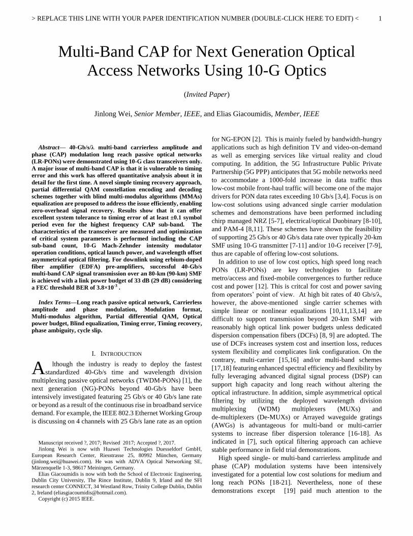
Fig. 1 depicts the setup for a LR 40 Gb/s lane rate multi-band
CAP NG-PON system experiment. The transmitter contains an
offline multi-band CAP signal generator, an 80-GS/s
digital-to-analog convertor (DAC), a single-ended linear driver,
and a 10-G tunable transmitter assembly (TTA). The TTA
consists of a tunable laser (with 50-GHz WDM grid granularity)
operating at 1543.3 nm and an InP dual drive Mach–Zehnder
intensity modulator (MZM) with a bandwidth of around 13
GHz [11]. Although the TTA is more expensive than a 10-G
directly modulated laser (DML) [5-7], it keeps a lower system
operation and maintanence cost especially when DWDM is
considered in green field deployments. Following the MZM, a
tunable optical bandpass filter (OBPF) with a 3-dB bandwidth
of approximately 39 GHz is adopted and its output is amplified
by a booster erbium-doped fiber amplifier (EDFA). The OBPF
has a filtering profile very similar to a 50-GHz grid WDM
MUX [23]. The OBPF is tuned to generate a frequency offset
between the laser frequency and the MUX center frequency,
leading to a VSB multi-band CAP signal [17-19]. The VSB
signal can significantly increase the tolerance to fiber CD
compared to the double sideband (DSB) case. The frequency
offset is optimized in order to maximize the system
performance. A variable optical attenuator (VOA) at the output
of the booster EDFA adjusts the optical power launched into
the fiber link. After transmission over an SMF link up to 90 km,
a combined optical receiver consists of VOAs, pre-amplifier
EDFA, a 40-GHz bandwidth OBPF with identical
configuration of the transmitter OBPF, and a 10-G PIN-TIA is
utilized to detect the received optical signal. A VOA is used to
optimize the input power injected into the PIN-TIA. Note that
the pre-amplifier EDFA can be co-located with and prior to a
De-MUX or AWG in the remote node in optical amplified
LR-PONs, thus the cost can be shared by multiple subscribers.
The detected multi-band CAP signal is then converted into a
digital signal by an ADC sampling at 80 GS/s. The digital
signal is then sent to a computer and undergoes offline signal
processing.
The detailed process of offline DSPs for the transmitter and
the receiver is also presented in Fig. 1, which is similar to that
presented in [17]. The transmitter offline DSP includes a
serial-to-parallel (S/P) convertor, a Levin Campello
algorithm-based bit/power loading module needed at the
beginning of the communication, differential QAM encoders
varying from differential binary phase shift keying (DBPSK),
DQPSK to partial differential QAM-32 to convert bit streams
into complex symbols, orthogonal square-root raised cosine
Fig. 1. Experimental setup of a 40 Gb/s lane rate NG-PON downstream link using multi-band CAP. The inset shows the 3-dB bandwidth measurement of the
system for an optical back to back link.
> REPLACE THIS LINE WITH YOUR PAPER IDENTIFICATION NUMBER (DOUBLE-CLICK HERE TO EDIT) <
3
(SRRC) shaping filter pairs containing inphase(I) and
quadrature (Q) channels with a roll-off coefficient of α = 0.1 at
its assigned center frequency kf (k = 1, 2, …, N), and an
addition operation to add symbols of all sub-bands. N is the
sub-band count. The added signal is then clipped to achieve a
peak-to-average ratio of 11 dB and quantized to the amplitude
range (0 to 255) required by the DAC. The receiver offline DSP
consists of matched SRRC filter pairs to separate the sub-band
signals, a timing recovery module to obtain the optimum
sampling point for each sub-band signal, a re-sampler that
generates two samples per symbol, a simple blind 14-tap T/2
space (T is the symbol time period) MMA-based feedforward
equalizer (FFE), whose output is directly fed to the following
partial differential QAM decoders to convert complex symbols
into bit streams. The bit error ratio (BER) prior to FEC is the
result of a one-on-one comparison between the transmitted and
the recovered bits. The CAP signal baud rate is 1GBaud,
leading to an oversampling of 80. The matched SRRC filters
have 880 taps (11 symbols length) and a roll-off coefficient of
0.1. Note that in real implementations, however, the ADC
sampling speed can be reduced significantly and the matched
filters of sub-bands at lower frequencies need much less
number of taps [24].
Note that currently, NG PON bit rates are not yet clear,
especially for the 40-G case. We thus assume two possible FEC
schemes: a low complex RS(255,223) with 14.35% overhead,
6.56 dB net coding gain and FEC threshold BER of 10-3
, which
was adopted by 10G-EPON standard, and a more complex high
gain hard-decision FEC with threshold BER of 3.8×10⁻³
and
7%- overhead [25]. We denote these two schemes as FEC1 and
FEC2, respectively, in this paper. No extra DSP overhead is
needed since the receiver DSP is performed in a completely
blind manner, as explained in the following subsection. In
addition, the wavelength plan for 40-G per wavelength NG
PON is not clear neither. Semiconductor optical amplifier
instead of EDFA shown in Fig. 1 could be used if O-band
wavelength plan is considered.
B. Timing Recovery
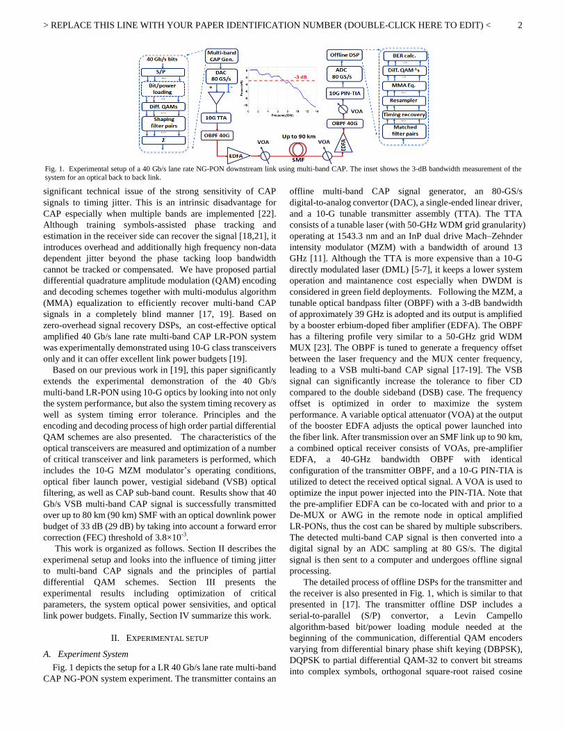
One of the key contributions of this work is to address the
timing recovery issue with multi-band CAP. As indicated in
previous work [22], CAP system is sensitive to timing jitter.
For multi-band CAP, this technical issue especially applies to
sub-bands at high frequencies. The reason can be explained by
simple mathematics: a timing error of Δt (-T/2<Δt<T/2) will
cause a phase offset of Δϕk (k = 1,2,3,…,N) to the k-th sub-band
received signal constellation after matched filters. The phase
offset is given by [22]
tfkk 2 (1)
Assuming no guard band between each adjacent sub-bands, the
center frequency of the k-th sub-band is kf = (1+α)·(2k− 1)/2T.
Then Eq. (1) can be rewritten as
T
tkk
)12)(α1( (2)
According to Eq. (2), the phase offset is linearly proportional
to two factors: 1) the timing error normalized to symbol time
period, and 2) the sub-band index. Fig. 2 shows the phase offset
dependence on the timing error for various sub-bands. It is very
interesting to notice that for sub-bands at high frequencies, a
very small timing error can cause significant phase offset. For
example, for the 7th
and 14th sub-band, timing error of 0.05
symbol period and 0.025 symbol period would bring about over
π/2 phase offset.
For square QAM constellations, MMA equalization [26,27]
is an efficient blind method for constellation recovery which is
more cost effective and does not require retraining after sudden
channel changes, since the optical channel is not highly time
varying. Square QAM constellations are rotationally symmetric
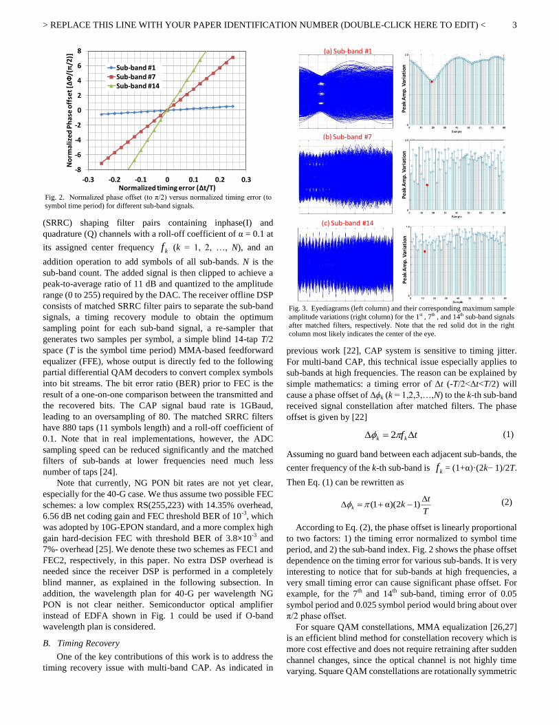
Fig. 3. Eyediagrams (left column) and their corresponding maximum sample
amplitude variations (right column) for the 1st , 7th , and 14th sub-band signals
after matched filters, respectively. Note that the red solid dot in the right
column most likely indicates the center of the eye.
(a) Sub-band #1
(b) Sub-band #7
(c) Sub-band #14
Pe
akA
mp
. Var
iati
on
Pe
akA
mp
. Var
iati
on
Pe
akA
mp
. Var
iati
on
Fig. 2. Normalized phase offset (to π/2) versus normalized timing error (to
symbol time period) for different sub-band signals.
-8
-6
-4
-2
0
2
4
6
8
-0.3 -0.2 -0.1 0 0.1 0.2 0.3
No
rmal
ized
Ph
ase
off
set
[ΔФ
/(π
/2)]
Normalized timing error (Δt/T)
Sub-band #1Sub-band #7Sub-band #14
> REPLACE THIS LINE WITH YOUR PAPER IDENTIFICATION NUMBER (DOUBLE-CLICK HERE TO EDIT) <
4
by the angle π/2 (π for DBPSK). This means errors that are
multiples of π/2 in the phase are undetectable. This is so called
π/2 phase ambiguity that absolute phase rotation of
(M =±1, ±2, ±3,… and M ≠ 4j and j is an integer number) of the
constellation introduced by the channel cannot be recovered by
the equalizer, also referred to as cycle slip in the remainder of
the paper. This consequently brings about very stringent
requirements on timing recovery especially for high frequency
sub-bands, otherwise phase offset tracking and estimation must
be conducted since timing error is usually time dependent [22].
Fig. 3 left column illustrates the matched filters’ output
signals whose information will be used to conduct timing
recovery via extracting the optimum sample point without aid
of training symbols. Since there are no clock tones available in
multi-CAP spectrum due to strong Nyquist filtering, the simple
conventional square timing recovery approach [28] cannot be
adopted here. We propose a simple approach for the optimum
timing phase search as shown in Fig. 3 right column. This
approach utilizes the statistical property that the optimum
sampling point has approximately the lowest peak amplitude
variation (PAV) by observing the sample amplitude over a
number of symbol periods, as indicated by the eye diagrams in
Fig. 3. For M symbol periods, suppose the i-th sampling
position of each symbol period corresponding to the k-th
sub-band contains samples , where the range of i is
determined by the oversampling, which is 80 here thus i = 1, 2,
3, …80. The PAV of the i-th sampling position is defined as
. Then the optimum sampling
point of each sub-band signal is obtained which corresponds to
the minimum , as indicated by the red solid dots in the
right column plots of Fig. 3. The complexity of the approach
almost linearly proportional to the number of symbol periods
considered since only search algorithm is used to obtain the
PAV of each sampling position. Through the paper, only 100
symbol periods of samples were used for the timing recovery
algorithm. However, this approach still has problem with
dealing with CAP signals at high frequency sub-bands. As
indicated in Fig. 3, the amplitude peak varation property is
weakened in the 7th
sub-band and beyond. And timing error
would easily cause cycle slip issue for the following MMA
equalizer.
To efficiently address the cycle slip issue, (partial)
differential QAM encoding and decoding schemes can be used
due to their natural immunity to phase offset. DBPSK and
DQPSK are differential coding schemes widely used in various
communication systems. Higher order QAMs can be encoded
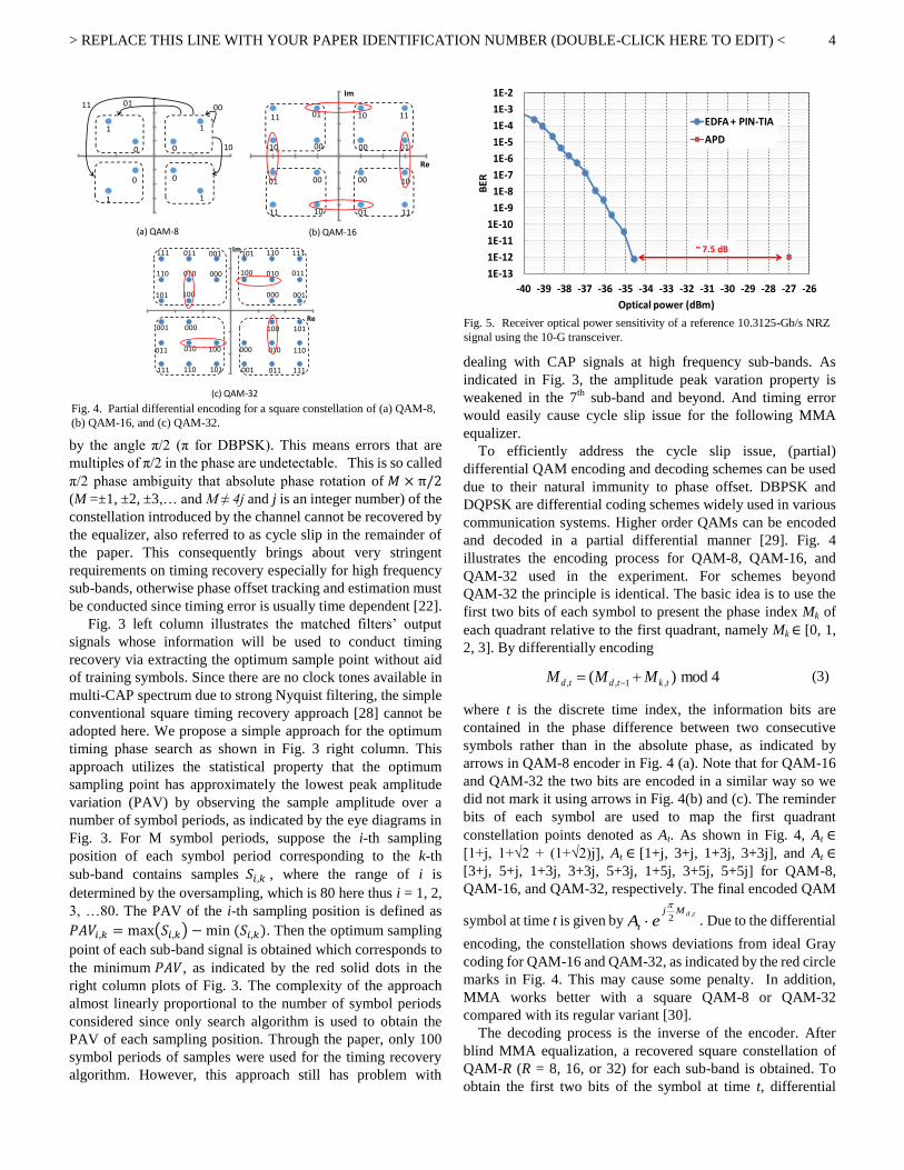
and decoded in a partial differential manner [29]. Fig. 4
illustrates the encoding process for QAM-8, QAM-16, and
QAM-32 used in the experiment. For schemes beyond
QAM-32 the principle is identical. The basic idea is to use the
first two bits of each symbol to present the phase index Mk of
each quadrant relative to the first quadrant, namely Mk [0, 1,
2, 3]. By differentially encoding
4mod)( ,1,, tktdtd MMM (3)
where t is the discrete time index, the information bits are
contained in the phase difference between two consecutive
symbols rather than in the absolute phase, as indicated by
arrows in QAM-8 encoder in Fig. 4 (a). Note that for QAM-16
and QAM-32 the two bits are encoded in a similar way so we
did not mark it using arrows in Fig. 4(b) and (c). The reminder
bits of each symbol are used to map the first quadrant
constellation points denoted as At. As shown in Fig. 4, At
[1+j, 1+√2 + (1+√2)j], At [1+j, 3+j, 1+3j, 3+3j], and At
[3+j, 5+j, 1+3j, 3+3j, 5+3j, 1+5j, 3+5j, 5+5j] for QAM-8,
QAM-16, and QAM-32, respectively. The final encoded QAM
symbol at time t is given bytdMj
t eA,
2
. Due to the differential
encoding, the constellation shows deviations from ideal Gray
coding for QAM-16 and QAM-32, as indicated by the red circle
marks in Fig. 4. This may cause some penalty. In addition,
MMA works better with a square QAM-8 or QAM-32
compared with its regular variant [30].
The decoding process is the inverse of the encoder. After
blind MMA equalization, a recovered square constellation of
QAM-R (R = 8, 16, or 32) for each sub-band is obtained. To
obtain the first two bits of the symbol at time t, differential
Fig. 5. Receiver optical power sensitivity of a reference 10.3125-Gb/s NRZ
signal using the 10-G transceiver.
1E-13
1E-12
1E-11
1E-10
1E-9
1E-8
1E-7
1E-6
1E-5
1E-4
1E-3
1E-2
-40 -39 -38 -37 -36 -35 -34 -33 -32 -31 -30 -29 -28 -27 -26
BE
R
Optical power (dBm)
EDFA + PIN-TIA
APD
~ 7.5 dB
Fig. 4. Partial differential encoding for a square constellation of (a) QAM-8,
(b) QAM-16, and (c) QAM-32.
Im
Re
000 001
010 011100
101 110 111001
000
000
000
001
001
010
010 010
100
100
100
101
101
101
111 111
111
110
110
110
011
011
011
(a) QAM-8 (b) QAM-16
(c) QAM-32
0
1
0
0 0
1
1 1
0001
10
11
Im
Re
00
1111
11 11
10
10
10
10
01
01
01
01
0000
00
> REPLACE THIS LINE WITH YOUR PAPER IDENTIFICATION NUMBER (DOUBLE-CLICK HERE TO EDIT) <
5
decoding is needed based on
4mod)~~
(~
1,,, tdtdtk MMM (4)
The remainder (log2R – 2) bits of each symbol are recovered
according to its corresponding amplitude At in the first
quadrant. The drawback of (partial) differential QAM is that it
will cause penalty due to error propagation and non ideal Grey
coding. For square QAM-R, the theoretical penalty defined as
the bit error probability ratio of the differentially coded system
to the non-differentially coded system is given by
2log1
2( 1)
R
R
[29], which corresponds to 3 dB and 2.2 dB
for QAM-4 and QAM-16, respectively.
The partial differential QAM encoding/decoding schemes
together with MMA equalizer relax significantly the
requirement on timing recovery and bring about zero-overhead
for receiver DSPs.
Note that, strictly speaking, the above-mentioned timing
issue is a timing offset issue. Timing jitter in this context could
be defined as the short-time variation of the optimum sampling
point. The differential coding itself can only solve the cycle slip
problem but will not track phase noise. The blind MMA can
track phase noise to some extent if the phase noise causes a
constellation phase rotation within [-π/2, π/2], beyond which
cycle slip occurs and coding deals with it. In spite of this, it may
still cause penalty when jitter occurs since jitter leads to CAP
constellations with not only phase rotation (can be corrected)
but also with points more scattered [22]. On this point, K-mean
or other nonlinear machine learning equalization schemes may
offer better performance than linear MMA [31-34]. Note that
equalizers alone can not address cycle slip issue. On the other
hand, since the system uses direct detection and transversal
filters for sub-band signal de-multiplexing, no optical or RF
local oscillator is involved. It would not expect a very
strong/fast phase noise for such a system.
III. EXPERIMENTAL RESULTS
A. 10-G Optical Transceiver
The 10-G TTA and the pre-amplified PIN-TIA are the key
components that enable low cost realization of the 40-Gb/s
LR-PON system proposed here. On one hand, the optical
transmitter takes the majority cost of the overall transceiver
cost and the cost is approximately proportionally depends on
the bandwidth [13]. On the other hand, the low-cost optical
transceiver is one of the major limiting factors determining the
achievable performance. As shown in Fig. 1 inset, the overall
bandwidth is only about 7-GHz for optical back to back case.
By using the 10-G transceiver, Fig. 5 presents the optical power
sensitivity for a 10.3125-Gb/s reference NRZ signal. The
measurement is based on an optical back-to-back (B2B) setup
including a PRBS pattern generator (PPG) at 10.3125 Gb/s in
the transmitter and a BERT in the receiver. The receiver
sensitivity for a BER of 10-12
for the 10.125-Gb/s NRZ signal is
approximately -34.5 dBm using no FECs. As a reference, the
optical power sensitivity of a commercially available 10-G
avalanche photodiode (APD) receiver is also presented in Fig. 5
[35], which shows about 7.5-dB penalty at BER of 10-12
relative
to the EDFA + PIN-TIA receiver. This penalty agrees well with
the theoretical estimation made in [11].
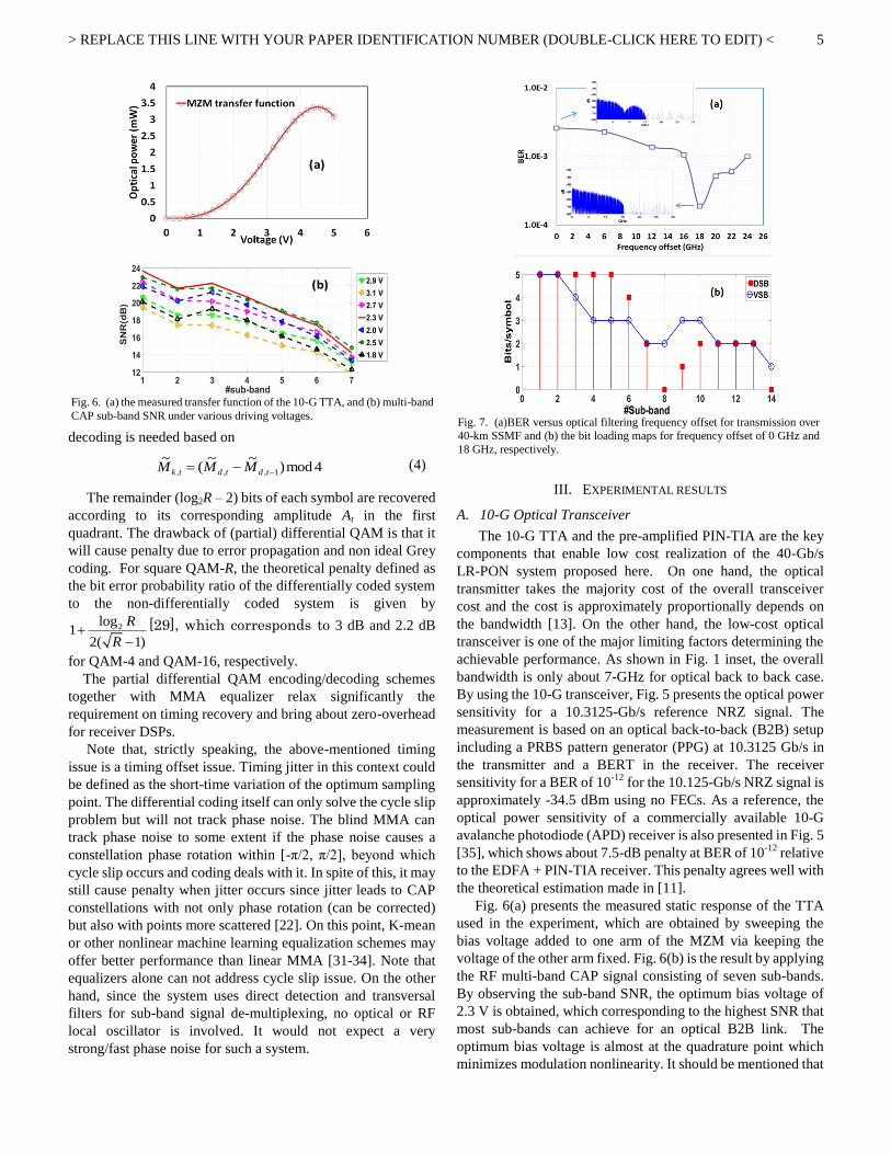
Fig. 6(a) presents the measured static response of the TTA
used in the experiment, which are obtained by sweeping the
bias voltage added to one arm of the MZM via keeping the
voltage of the other arm fixed. Fig. 6(b) is the result by applying
the RF multi-band CAP signal consisting of seven sub-bands.
By observing the sub-band SNR, the optimum bias voltage of
2.3 V is obtained, which corresponding to the highest SNR that
most sub-bands can achieve for an optical B2B link. The
optimum bias voltage is almost at the quadrature point which
minimizes modulation nonlinearity. It should be mentioned that
Fig. 6. (a) the measured transfer function of the 10-G TTA, and (b) multi-band
CAP sub-band SNR under various driving voltages.
(a)
(b)
Fig. 7. (a)BER versus optical filtering frequency offset for transmission over
40-km SSMF and (b) the bit loading maps for frequency offset of 0 GHz and
18 GHz, respectively.
> REPLACE THIS LINE WITH YOUR PAPER IDENTIFICATION NUMBER (DOUBLE-CLICK HERE TO EDIT) <
6
the MZM supports differential input driving signal, in which
case the MZM has zero chirp. However, due to the lack of an
RF amplifier with differential output in lab, the MZM is driven
by a single-ended multi-band CAP signal. As a result, the MZM
behaves negative chirp.
B. Optimization of Optical Filtering
The OBPFs used in the setup in Fig. 1 can be used to
generate a VSB multi-band CAP signal, which is realized by
tuning the wavelength of the laser integrated within the TTA. In
practice, (De-)MUXs can be used to replace OBPFs. Fig. 7(a)
examines the dependence of the system BER performance on
the frequency offset between the laser wavelength and the
OBPF central wavelength. An optimum frequency offset of 18
GHz is obtained, below which the BER degradation is due to
fiber chromatic dispersion, which causes a frequency notch
within the signal spectrum as indicated by the upper inset of
Fig. 7(a). Consequently the surrounding sub-bands adjacent to
the notch must use low order modulations or even completely
dropped off, as shown in the corresponding bit loading map in
Fig. 7(b). In order to achieve a fixed bit rate of 40 Gb/s, low
frequency sub-bands have to adopt high order modulation
formats such as QAM-32, leading to degradation in optical
power sensitivity. The lower inset in Fig. 7(a) shows that the
optimum frequency offset enables a signal spectrum without
distortions and moderate order modulation schemes are can be
allocated to most sub-bands [see Fig. 7(b)], which improves the
overall optical power sensitivity. Beyond the optimum
frequency offset, performance degradation is attributed to
unwanted filtering of the other sideband.
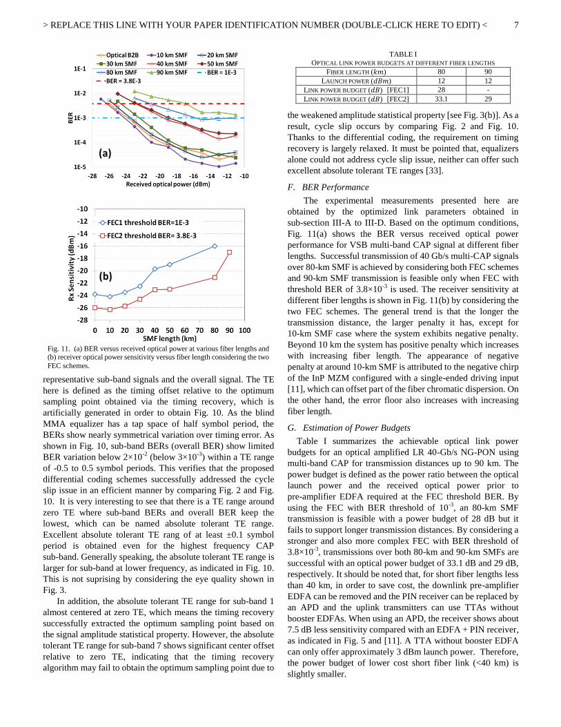
C. Optimization of Optical Launch Power
The optical power launched into the fiber link has a
straightforward influence on the achievable system power
budget. Fig. 8 explores the relationship between system BER
performance and optical launch power. It shows that the
optimum launch power is approximately 12 dBm. Below the
optimum launch power the system is limited by achievable
received optical power, as indicated in Fig. 8. Further increase
in launch power causes Brillouin scattering thus serious system
degradation occurs.
D. Effect of Sub-band Count
The sub-band count of multi-CAP is of important concern
regarding system performance and DSP complexity [24]. Fig. 9
looks into the effect of sub-band count on the receiver optical
power sensitivity. The performance developing trend indicates
that the error floor reduces with increasing sub-band count and
a sub-band count of 14 brings about the lowest error floor. The
physics underpinning such trend is because more sub-bands
enable the system with smaller granularity to better adapt itself
to the channel conditions. Meantime, the optical power
sensitivity at BER of 10-3
increases with increasing sub-band
count and saturates at sub-band count of 7. This is attributed to
two reasons: the use of an optical VSB configuration and the
stronger sub-band × sub-band intermixing presents for a larger
sub-band count. Overall, a sub-band count of 14 brings about
both optimum power sensitivity and error floor, which is used
for the following measurement.
E. Tolerance to Timing Error
Based on the optimum parameters obtained above, this
sub-section evaluates the system tolerance to timing error (T
E) by using the coding and algorithms introduced in Section II.
Fig. 10 illustrates the BER variations with the TE for
Fig. 9. System BER versus optical power for multi-band CAP having
various sub-band count. Results are based on 40-km SMF link and
asymmetric optical filtering with 18 GHz frequency offset.
1.0E-4
1.0E-3
1.0E-2
-26 -24 -22 -20 -18 -16 -14 -12 -10
BER
Received optical power (dB)
VSB, 1 band VSB, 3 bandsVSB, 7 bands VSB, 14 bandsVSB, 28 bands
Fig. 8. The dependence of system BER on optical launch power for a 40-km
SMF link. The received optical power corresponding to each launch power is
also presented.
-30
-28
-26
-24
-22
-20
-18
-16
1.0E-4
1.0E-3
1.0E-2
1.0E-1
0 2 4 6 8 10 12 14 16
RO
P (
dB
m)
BER
Launch power (dBm)
BERReceived optical power
Fig. 10. Sub-band and overall BER versus timing error normaliyed to symbol period. Results are based on 40-km SMF link with asymmetric
optical filtering with 18 GHz frequency offset and a received optical power
of -19 dBm. Note that, for sub-bands 7 and 14, the lowest BER is actually 0
which is replaced with a fixed BER value for display convenience.
> REPLACE THIS LINE WITH YOUR PAPER IDENTIFICATION NUMBER (DOUBLE-CLICK HERE TO EDIT) <
7
representative sub-band signals and the overall signal. The TE
here is defined as the timing offset relative to the optimum
sampling point obtained via the timing recovery, which is
artificially generated in order to obtain Fig. 10. As the blind
MMA equalizer has a tap space of half symbol period, the
BERs show nearly symmetrical variation over timing error. As
shown in Fig. 10, sub-band BERs (overall BER) show limited
BER variation below 2×10⁻²
(below 3×10⁻³
) within a TE range
of -0.5 to 0.5 symbol periods. This verifies that the proposed
differential coding schemes successfully addressed the cycle
slip issue in an efficient manner by comparing Fig. 2 and Fig.
10. It is very interesting to see that there is a TE range around
zero TE where sub-band BERs and overall BER keep the
lowest, which can be named absolute tolerant TE range.
Excellent absolute tolerant TE rang of at least ±0.1 symbol
period is obtained even for the highest frequency CAP
sub-band. Generally speaking, the absolute tolerant TE range is
larger for sub-band at lower frequency, as indicated in Fig. 10.
This is not suprising by considering the eye quality shown in
Fig. 3.
In addition, the absolute tolerant TE range for sub-band 1
almost centered at zero TE, which means the timing recovery
successfully extracted the optimum sampling point based on
the signal amplitude statistical property. However, the absolute
tolerant TE range for sub-band 7 shows significant center offset
relative to zero TE, indicating that the timing recovery
algorithm may fail to obtain the optimum sampling point due to
the weakened amplitude statistical property [see Fig. 3(b)]. As a
result, cycle slip occurs by comparing Fig. 2 and Fig. 10.
Thanks to the differential coding, the requirement on timing
recovery is largely relaxed. It must be pointed that, equalizers
alone could not address cycle slip issue, neither can offer such
excellent absolute tolerant TE ranges [33].
F. BER Performance
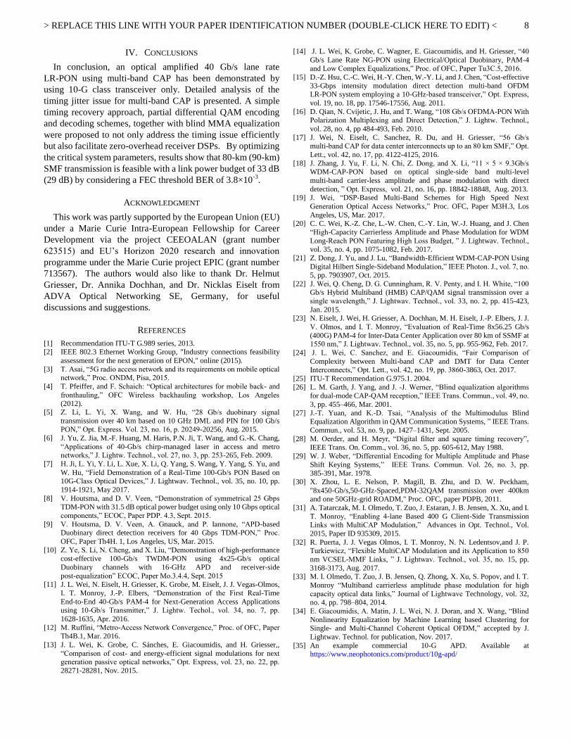
The experimental measurements presented here are
obtained by the optimized link parameters obtained in
sub-section III-A to III-D. Based on the optimum conditions,
Fig. 11(a) shows the BER versus received optical power
performance for VSB multi-band CAP signal at different fiber
lengths. Successful transmission of 40 Gb/s multi-CAP signals
over 80-km SMF is achieved by considering both FEC schemes
and 90-km SMF transmission is feasible only when FEC with
threshold BER of 3.8×10⁻³
is used. The receiver sensitivity at
different fiber lengths is shown in Fig. 11(b) by considering the
two FEC schemes. The general trend is that the longer the
transmission distance, the larger penalty it has, except for
10-km SMF case where the system exhibits negative penalty.
Beyond 10 km the system has positive penalty which increases
with increasing fiber length. The appearance of negative
penalty at around 10-km SMF is attributed to the negative chirp
of the InP MZM configured with a single-ended driving input
[11], which can offset part of the fiber chromatic dispersion. On
the other hand, the error floor also increases with increasing
fiber length.
G. Estimation of Power Budgets
Table I summarizes the achievable optical link power
budgets for an optical amplified LR 40-Gb/s NG-PON using
multi-band CAP for transmission distances up to 90 km. The
power budget is defined as the power ratio between the optical
launch power and the received optical power prior to
pre-amplifier EDFA required at the FEC threshold BER. By
using the FEC with BER threshold of 10-3
, an 80-km SMF
transmission is feasible with a power budget of 28 dB but it
fails to support longer transmission distances. By considering a
stronger and also more complex FEC with BER threshold of
3.8×10⁻³
, transmissions over both 80-km and 90-km SMFs are
successful with an optical power budget of 33.1 dB and 29 dB,
respectively. It should be noted that, for short fiber lengths less
than 40 km, in order to save cost, the downlink pre-amplifier
EDFA can be removed and the PIN receiver can be replaced by
an APD and the uplink transmitters can use TTAs without
booster EDFAs. When using an APD, the receiver shows about
7.5 dB less sensitivity compared with an EDFA + PIN receiver,
as indicated in Fig. 5 and [11]. A TTA without booster EDFA
can only offer approximately 3 dBm launch power. Therefore,
the power budget of lower cost short fiber link (<40 km) is
slightly smaller.
Fig. 11. (a) BER versus received optical power at various fiber lengths and (b) receiver optical power sensitivity versus fiber length considering the two
FEC schemes.
(a)
(b)
TABLE I
OPTICAL LINK POWER BUDGETS AT DIFFERENT FIBER LENGTHS
FIBER LENGTH ( ) 80 90
LAUNCH POWER ( ) 12 12
LINK POWER BUDGET ( ) [FEC1] 28 -
LINK POWER BUDGET ( ) [FEC2] 33.1 29
> REPLACE THIS LINE WITH YOUR PAPER IDENTIFICATION NUMBER (DOUBLE-CLICK HERE TO EDIT) <
8
IV. CONCLUSIONS
In conclusion, an optical amplified 40 Gb/s lane rate
LR-PON using multi-band CAP has been demonstrated by
using 10-G class transceiver only. Detailed analysis of the
timing jitter issue for multi-band CAP is presented. A simple
timing recovery approach, partial differential QAM encoding
and decoding schemes, together with blind MMA equalization
were proposed to not only address the timing issue efficiently
but also facilitate zero-overhead receiver DSPs. By optimizing
the critical system parameters, results show that 80-km (90-km)
SMF transmission is feasible with a link power budget of 33 dB
(29 dB) by considering a FEC threshold BER of 3.8×10⁻³
.
ACKNOWLEDGMENT
This work was partly supported by the European Union (EU)
under a Marie Curie Intra-European Fellowship for Career
Development via the project CEEOALAN (grant number
623515) and EU’s Horizon 2020 research and innovation
programme under the Marie Curie project EPIC (grant number
713567). The authors would also like to thank Dr. Helmut
Griesser, Dr. Annika Dochhan, and Dr. Nicklas Eiselt from
ADVA Optical Networking SE, Germany, for useful
discussions and suggestions.
REFERENCES
[1] Recommendation ITU-T G.989 series, 2013.
[2] IEEE 802.3 Ethernet Working Group, "Industry connections feasibility
assessment for the next generation of EPON," online (2015).
[3] T. Asai, “5G radio access network and its requirements on mobile optical network,” Proc. ONDM, Pisa, 2015.
[4] T. Pfeiffer, and F. Schaich: “Optical architectures for mobile back- and
fronthauling,” OFC Wireless backhauling workshop, Los Angeles (2012).
[5] Z. Li, L. Yi, X. Wang, and W. Hu, “28 Gb/s duobinary signal
transmission over 40 km based on 10 GHz DML and PIN for 100 Gb/s PON,” Opt. Express. Vol. 23, no. 16, p. 20249-20256, Aug. 2015.
[6] J. Yu, Z. Jia, M.-F. Huang, M. Haris, P.N. Ji, T. Wang, and G.-K. Chang,
“Applications of 40-Gb/s chirp-managed laser in access and metro networks,” J. Lightw. Technol., vol. 27, no. 3, pp. 253-265, Feb. 2009.
[7] H. Ji, L. Yi, Y. Li, L. Xue, X. Li, Q. Yang, S. Wang, Y. Yang, S. Yu, and
W. Hu, “Field Demonstration of a Real-Time 100-Gb/s PON Based on 10G-Class Optical Devices,” J. Lightwav. Technol., vol. 35, no. 10, pp.
1914-1921, May 2017.
[8] V. Houtsma, and D. V. Veen, “Demonstration of symmetrical 25 Gbps TDM-PON with 31.5 dB optical power budget using only 10 Gbps optical
components,” ECOC, Paper PDP. 4.3, Sept. 2015.
[9] V. Houtsma, D. V. Veen, A. Gnauck, and P. Iannone, “APD-based Duobinary direct detection receivers for 40 Gbps TDM-PON,” Proc.
OFC, Paper Th4H. 1, Los Angeles, US, Mar. 2015.
[10] Z. Ye, S. Li, N. Cheng, and X. Liu, “Demonstration of high-performance cost-effective 100-Gb/s TWDM-PON using 4x25-Gb/s optical
Duobinary channels with 16-GHz APD and receiver-side
post-equalization” ECOC, Paper Mo.3.4.4, Sept. 2015 [11] J. L. Wei, N. Eiselt, H. Griesser, K. Grobe, M. Eiselt, J. J. Vegas-Olmos,
I. T. Monroy, J.-P. Elbers, “Demonstration of the First Real-Time
End-to-End 40-Gb/s PAM-4 for Next-Generation Access Applications using 10-Gb/s Transmitter,” J. Lightw. Techol., vol. 34, no. 7, pp.
1628-1635, Apr. 2016.
[12] M. Ruffini, “Metro-Access Network Convergence,” Proc. of OFC, Paper Th4B.1, Mar. 2016.
[13] J. L. Wei, K. Grobe, C. Sánches, E. Giacoumidis, and H. Griesser,,
“Comparison of cost- and energy-efficient signal modulations for next generation passive optical networks,” Opt. Express, vol. 23, no. 22, pp.
28271-28281, Nov. 2015.
[14] J. L. Wei, K. Grobe, C. Wagner, E. Giacoumidis, and H. Griesser, “40
Gb/s Lane Rate NG-PON using Electrical/Optical Duobinary, PAM-4
and Low Complex Equalizations,” Proc. of OFC, Paper Tu3C.5, 2016.
[15] D.-Z. Hsu, C.-C. Wei, H.-Y. Chen, W.-Y. Li, and J. Chen, “Cost-effective
33-Gbps intensity modulation direct detection multi-band OFDM LR-PON system employing a 10-GHz-based transceiver,” Opt. Express,
vol. 19, no. 18, pp. 17546-17556, Aug. 2011.
[16] D. Qian, N. Cvijetic, J. Hu, and T. Wang, “108 Gb/s OFDMA-PON With Polarization Multiplexing and Direct Detection,” J. Lightw. Technol.,
vol. 28, no. 4, pp 484-493, Feb. 2010.
[17] J. Wei, N. Eiselt, C. Sanchez, R. Du, and H. Griesser, “56 Gb/s multi-band CAP for data center interconnects up to an 80 km SMF,” Opt.
Lett., vol. 42, no. 17, pp. 4122-4125, 2016.
[18] J. Zhang, J. Yu, F. Li, N. Chi, Z. Dong, and X. Li, “11 × 5 × 9.3Gb/s WDM-CAP-PON based on optical single-side band multi-level
multi-band carrier-less amplitude and phase modulation with direct
detection, ” Opt. Express, vol. 21, no. 16, pp. 18842-18848, Aug. 2013. [19] J. Wei, “DSP-Based Multi-Band Schemes for High Speed Next
Generation Optical Access Networks,” Proc. OFC, Paper M3H.3, Los
Angeles, US, Mar. 2017. [20] C. C. Wei, K.-Z. Che, L.-W. Chen, C.-Y. Lin, W.-J. Huang, and J. Chen
“High-Capacity Carrierless Amplitude and Phase Modulation for WDM
Long-Reach PON Featuring High Loss Budget, ” J. Lightwav. Technol., vol. 35, no. 4, pp. 1075-1082, Feb. 2017.
[21] Z. Dong, J. Yu, and J. Lu, “Bandwidth-Efficient WDM-CAP-PON Using
Digital Hilbert Single-Sideband Modulation,” IEEE Photon. J., vol. 7, no. 5, pp. 7903907, Oct. 2015.
[22] J. Wei, Q. Cheng, D. G. Cunningham, R. V. Penty, and I. H. White, “100 Gb/s Hybrid Multiband (HMB) CAP/QAM signal transmission over a
single wavelength,” J. Lightwav. Technol., vol. 33, no. 2, pp. 415-423,
Jan. 2015. [23] N. Eiselt, J. Wei, H. Griesser, A. Dochhan, M. H. Eiselt, J.-P. Elbers, J. J.
V. Olmos, and I. T. Monroy, “Evaluation of Real-Time 8x56.25 Gb/s
(400G) PAM-4 for Inter-Data Center Application over 80 km of SSMF at 1550 nm,” J. Lightwav. Technol., vol. 35, no. 5, pp. 955-962, Feb. 2017.
[24] J. L. Wei, C. Sanchez, and E. Giacoumidis, “Fair Comparison of
Complexity between Multi-band CAP and DMT for Data Center Interconnects,” Opt. Lett., vol. 42, no. 19, pp. 3860-3863, Oct. 2017.
[25] ITU-T Recommendation G.975.1. 2004.
[26] L. M. Garth, J. Yang, and J. -J. Werner, “Blind equalization algorithms for dual-mode CAP-QAM reception,” IEEE Trans. Commun., vol. 49, no.
3, pp. 455–466, Mar. 2001.
[27] J.-T. Yuan, and K.-D. Tsai, “Analysis of the Multimodulus Blind Equalization Algorithm in QAM Communication Systems, ” IEEE Trans.
Commun., vol. 53, no. 9, pp. 1427–1431, Sept. 2005.
[28] M. Oerder, and H. Meyr, “Digital filter and square timing recovery”, IEEE Trans. On. Comm., vol. 36, no. 5, pp. 605-612, May 1988.
[29] W. J. Weber, “Differential Encoding for Multiple Amplitude and Phase
Shift Keying Systems,” IEEE Trans. Commun. Vol. 26, no. 3, pp. 385-391, Mar. 1978.
[30] X. Zhou, L. E. Nelson, P. Magill, B. Zhu, and D. W. Peckham,
"8x450-Gb/s,50-GHz-Spaced,PDM-32QAM transmission over 400km and one 50GHz-grid ROADM," Proc. OFC, paper PDPB, 2011.
[31] A. Tatarczak, M. I. Olmedo, T. Zuo, J. Estaran, J. B. Jensen, X. Xu, and I.
T. Monroy, “Enabling 4-lane Based 400 G Client-Side Transmission Links with MultiCAP Modulation,” Advances in Opt. Technol., Vol.
2015, Paper ID 935309, 2015.
[32] R. Puerta, J. J. Vegas Olmos, I. T. Monroy, N. N. Ledentsov,and J. P. Turkiewicz, “Flexible MultiCAP Modulation and its Application to 850
nm VCSEL-MMF Links, ” J. Lightwav. Technol., vol. 35, no. 15, pp.
3168-3173, Aug. 2017. [33] M. I. Olmedo, T. Zuo, J. B. Jensen, Q. Zhong, X. Xu, S. Popov, and I. T.
Monroy “Multiband carrierless amplitude phase modulation for high
capacity optical data links,” Journal of Lightwave Technology, vol. 32, no. 4, pp. 798–804, 2014.
[34] E. Giacoumidis, A. Matin, J. L. Wei, N. J. Doran, and X. Wang, “Blind
Nonlinearity Equalization by Machine Learning based Clustering for
Single- and Multi-Channel Coherent Optical OFDM,” accepted by J.
Lightwav. Technol. for publication, Nov. 2017.
[35] An example commercial 10-G APD. Available at https://www.neophotonics.com/product/10g-apd/

> REPLACE THIS LINE WITH YOUR PAPER IDENTIFICATION NUMBER (DOUBLE-CLICK HERE TO EDIT) <
9
Jinlong Wei (S’09–M’11-SM’17) is currently a senior researcher in Huawei
Technologies Duesseldorf GmbH, European Research Center, Germany. He
received his PhD degree in Electronic Engineering from Bangor University,
Bangor, UK in 2010 and worked there afterwards as a post-doc researcher before joining the Centre for Photonics Systems of Cambridge University, UK
as a research associate in 2011. He was awarded a Marie Curie fellowship and
joined ADVA Optical Networking SE, Germany as a senior engineer in Sept. 2014. He has participated in about 10 European national and international
projects as well as projects with industry and realized a number of world-first
system demonstrations with his colleagues. He has been contributing to the next generation 100 Gigabit Ethernet study within IEEE802.3. He has authored
and coauthored over 120 journal and conference publications and 5 public
patents.
Elias Giacoumidis information is not available at the time of submission.
Top Related