WCDMA Direct Conversion Receiver Front End - EECS · WCDMA Direct Conversion Receiver Front End...
4
EECS 522, Final Project Report, Winter 2008 1 WCDMA Direct Conversion Receiver Front End Mohammad Adeel, and Chien-Hsun Lee Abstract—This paper presents a 2.14GHz RF front end for Wide-band Code Division Multiple Access (WCDMA) receiver. The receiver is based on direct conversion architecture and implements a low noise amplifier (LNA) and a quadrature mixer in 0.25μm CMOS process. The receiver achieves a noise figure (NF) of 8.93dB, provides a gain of 17.14dB, has an IIP3 of -15.04dB and dissipate 72.15mW at 2.5V. Index Terms—Direct conversion receiver, low-noise amplifier (LNA), mixer, wide-band code division multiple access (WCDMA) I. INTRODUCTION URRENTLY, wireless communication is evolving at an extremely rapid rate. Success of wireless systems depends heavily on their cost, form factor and power consumption. These system characteristics can be achieved by using CMOS processes which provide the ability to integrate more functionality at a lower cost on a single chip [1]. This paper describes an LNA and mixer for 2.14GHz WCDMA receiver systems. Direct conversion architecture is chosen because it is simple to implement, uses fewer components and is better suited for single-chip integration. These favorable characteristics of direct conversion provide a reasonable trade-off between receiver functionality, power consumption, and its form factor. Section II provides a brief description of the WCDMA architecture and its requirements. Next, section III discusses the LNA, its design technique and simulation results. Section IV is a description of mixer design and its results. Section V describes results obtained for the complete receiver (with integrated LNA and mixer). Finally, section VI presents our conclusions. II. WCDMA RECEIVER DESCRIPTION WCDMA is a very popular third generation cellular phone standard. WCDMA receiver mobile units operate in the 2110-2170MHz frequency band, have an allocated bandwidth of 5MHz and can provide data transmission rates up to 2Mb/s [2]. A block diagram of WCDMA front end is shown in Fig 1. The RF signal received by the antenna is filtered and is made differential. Next, the signal is amplified and is then down-converted to base-band along parallel in-phase (I) and RF Filter and Balun LNA Base Band Filter Base Band Filter VGA VGA I Q Fig. 1. Homodyne Receivr quadrature (Q) signal paths. This is an example of a homodyne receiver which eliminates the need for an intermediate frequency (IF) and thus, all associated components and their design challenges, including the image-reject issue. A fully differential signal path is chosen to reduce the coupling effect between receiver components and to reduce the amount of even order distortion [1]. III. LOW NOISE AMPLIFIER WCDMA applications require LNAs with extremely good performance measures. Noise figure (NF) has to be low since the receiver noise is determined by LNA noise. A 50Ω input match is required to terminate a transmission line form the antenna. This match is even more critical when an RF filter precedes the LNA as these filters are usually sensitive to the quality of the output match. Low power consumption requirement is dictated by the intended application (such as cell phones). Reasonable gain and linearity is also required for optimum receiver performance. The LNA presented here is 2.14GHz differential with inductively degenerated common source cascode configuration, Fig.2. Although, single ended LNAs have an advantage over differential in terms of power dissipation and noise figure but differential LNAs are more resistant to substrate coupled noise, even order distortion, and other sources of common mode disturbances such as noise on supply line. Cascode topology is used because cascode transistors, M1 and M2 provide reverse isolation and also reduce the effect of M1’s C [2]. Bias was provided using current mirrors. A 50Ω input match is provided but no output match is required. This is because all the details of the output stage (mixer) to the LNA are known and also because at the operating frequency of 2.14GHz length of the LNA is much smaller than the wavelength and therefore, transmission line phenomenon does not exist. Hence, minimal reflections will exist at the LNA/mixer interface thus, eliminating the need for an output match. gd A. Design Methodology Since power consumption is a critical factor for WCDMA applications so the design focused on obtaining lower power dissipation. Initially, power constrained noise optimization C
-
Upload
hoangxuyen -
Category
Documents
-
view
215 -
download
2
Transcript of WCDMA Direct Conversion Receiver Front End - EECS · WCDMA Direct Conversion Receiver Front End...
EECS 522, Final Project Report, Winter 2008 1
WCDMA Direct Conversion Receiver Front End Mohammad Adeel, and Chien-Hsun Lee
Abstract—This paper presents a 2.14GHz RF front end for
Wide-band Code Division Multiple Access (WCDMA) receiver. The receiver is based on direct conversion architecture and implements a low noise amplifier (LNA) and a quadrature mixer in 0.25μm CMOS process. The receiver achieves a noise figure (NF) of 8.93dB, provides a gain of 17.14dB, has an IIP3 of -15.04dB and dissipate 72.15mW at 2.5V.
Index Terms—Direct conversion receiver, low-noise amplifier (LNA), mixer, wide-band code division multiple access (WCDMA)
I. INTRODUCTION URRENTLY, wireless communication is evolving at an extremely rapid rate. Success of wireless systems depends
heavily on their cost, form factor and power consumption. These system characteristics can be achieved by using CMOS processes which provide the ability to integrate more functionality at a lower cost on a single chip [1].
This paper describes an LNA and mixer for 2.14GHz WCDMA receiver systems. Direct conversion architecture is chosen because it is simple to implement, uses fewer components and is better suited for single-chip integration. These favorable characteristics of direct conversion provide a reasonable trade-off between receiver functionality, power consumption, and its form factor.
Section II provides a brief description of the WCDMA architecture and its requirements. Next, section III discusses the LNA, its design technique and simulation results. Section IV is a description of mixer design and its results. Section V describes results obtained for the complete receiver (with integrated LNA and mixer). Finally, section VI presents our conclusions.
II. WCDMA RECEIVER DESCRIPTION WCDMA is a very popular third generation cellular phone
standard. WCDMA receiver mobile units operate in the 2110-2170MHz frequency band, have an allocated bandwidth of 5MHz and can provide data transmission rates up to 2Mb/s [2]. A block diagram of WCDMA front end is shown in Fig 1. The RF signal received by the antenna is filtered and is made differential. Next, the signal is amplified and is then down-converted to base-band along parallel in-phase (I) and
RF Filter and Balun LNA
Base Band Filter
Base Band Filter
VGA
VGA
I
Q
Fig. 1. Homodyne Receivr
quadrature (Q) signal paths. This is an example of a homodyne receiver which eliminates the need for an intermediate frequency (IF) and thus, all associated components and their design challenges, including the image-reject issue. A fully differential signal path is chosen to reduce the coupling effect between receiver components and to reduce the amount of even order distortion [1].
III. LOW NOISE AMPLIFIER WCDMA applications require LNAs with extremely good
performance measures. Noise figure (NF) has to be low since the receiver noise is determined by LNA noise. A 50Ω input match is required to terminate a transmission line form the antenna. This match is even more critical when an RF filter precedes the LNA as these filters are usually sensitive to the quality of the output match. Low power consumption requirement is dictated by the intended application (such as cell phones). Reasonable gain and linearity is also required for optimum receiver performance.
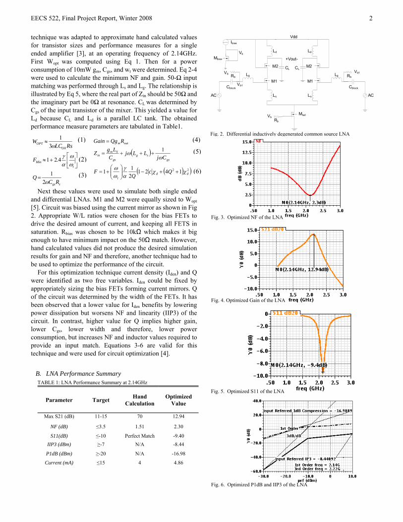
The LNA presented here is 2.14GHz differential with inductively degenerated common source cascode configuration, Fig.2. Although, single ended LNAs have an advantage over differential in terms of power dissipation and noise figure but differential LNAs are more resistant to substrate coupled noise, even order distortion, and other sources of common mode disturbances such as noise on supply line. Cascode topology is used because cascode transistors, M1 and M2 provide reverse isolation and also reduce the effect of M1’s C [2]. Bias was provided using current mirrors. A 50Ω input match is provided but no output match is required. This is because all the details of the output stage (mixer) to the LNA are known and also because at the operating frequency of 2.14GHz length of the LNA is much smaller than the wavelength and therefore, transmission line phenomenon does not exist. Hence, minimal reflections will exist at the LNA/mixer interface thus, eliminating the need for an output match.
gd
A. Design Methodology Since power consumption is a critical factor for WCDMA
applications so the design focused on obtaining lower power dissipation. Initially, power constrained noise optimization
C
EECS 522, Final Project Report, Winter 2008 2
sgs
tMin
OXOPT
RCQ
F
RsLCW
ω
ωω
αγ
ω
21
4.21
31
=
⎥⎦
⎤⎢⎣
⎡+≈
≈
technique was adapted to approximate hand calculated values for transistor sizes and performance measures for a single ended amplifier [3], at an operating frequency of 2.14GHz. First Wopt was computed using Eq 1. Then for a power consumption of 10mW gm, Cgs, and wt were determined. Eq 2-4 were used to calculate the minimum NF and gain. 50-Ω input matching was performed through Ls and Lg. The relationship is illustrated by Eq 5, where the real part of Zin should be 50Ω and the imaginary part be 0Ω at resonance. CL was determined by Cgs of the input transistor of the mixer. This yielded a value for Ld because CL and Ld is a parallel LC tank. The obtained performance measure parameters are tabulated in Table1.
Next these values were used to simulate both single ended and differential LNAs. M1 and M2 were equally sized to Wopt [5]. Circuit was biased using the current mirror as shown in Fig 2. Appropriate W/L ratios were chosen for the bias FETs to drive the desired amount of current, and keeping all FETS in saturation. Rbias was chosen to be 10kΩ which makes it big enough to have minimum impact on the 50Ω match. However, hand calculated values did not produce the desired simulation results for gain and NF and therefore, another technique had to be used to optimize the performance of the circuit.
For this optimization technique current density (Iden) and Q were identified as two free variables. Iden could be fixed by appropriately sizing the bias FETs forming current mirrors. Q of the circuit was determined by the width of the FETs. It has been observed that a lower value for Iden benefits by lowering power dissipation but worsens NF and linearity (IIP3) of the circuit. In contrast, higher value for Q implies higher gain, lower Cgs, lower width and therefore, lower power consumption, but increases NF and inductor values required to provide an input match. Equations 3-6 are valid for this technique and were used for circuit optimization [4].
B. LNA Performance Summary
AC
CL
Lg
Ld
Ls
Vdd
M2
M1Cblock
AC
CL
Lg
Ld
Ls
M2
M1Cblock
+Vout-
Vb
Vb Vb1
Vb
Rb
RbRb
Vb1
Ibias
Mbias
Mtail
Fig. 2. Differential inductively degenerated common source LNA(1)
( )
( )( )22 1421211
1
ddt
gssg
gs
Smin
outm
QcQ
(4)
TABLE 1: LNA Performance Summary at 2.14GHz
Parameter Target Hand Calculation
OptimizedValue
Max S21 (dB) 11-15 70 12.94
NF (dB) ≤3.5 1.51 2.30
S11(dB) ≤-10 Perfect Match -9.40 IIP3 (dBm) ≥-7 N/A -8.44
P1dB (dBm) ≥-20 N/A -16.98
Current (mA) ≤15 4 4.86
F
CjLLj
CLgZ
RQgGain
χχαγ
ωω
ωω
++−⎟⎟⎠
⎞⎜⎜⎝
⎛+=
+++=
=
(5)(2)
(6)(3)
Fig. 3. Optimized NF of the LNA
Fig. 4. Optimized Gain of the LNA
Fig. 5. Optimized S11 of the LNA
Fig. 6. Optimized P1dB and IIP3 of the LNA
EECS 522, Final Project Report, Winter 2008 3
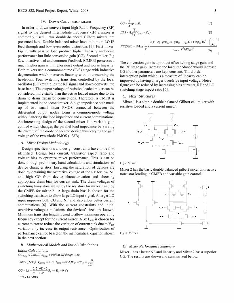
IV. DOWN-CONVERSION MIXER In order to down convert input high Radio-Frequency (RF)
signal to the desired intermediate frequency (IF) a mixer is commonly used. Two double-balanced Gilbert mixers are presented here. Double balanced mixer have minimum LO-IF feed-through and low even-order distortions [5]. First mixer, Fig 7, with passive load produce higher linearity and noise performance but little conversion gain (CG). Second mixer, Fig 8, with active load and common-feedback (CMFB) possesses a much higher gain with higher noise output and worse linearity. Both mixers use a common-source (C-S) stage with inductive degeneration which increases linearity without consuming the headroom. Four switching transistors controlled by the local oscillator (LO) multiplies the RF signal and down-converts it to base-band. The output voltage of resistive loaded mixer can be considered more stable than the active loaded mixer due to the drain to drain transistor connections. Therefore, a CMFB is implemented in the second mixer. A high impedance path made up of two small linear PMOS connected between the differential output nodes forms a common-mode voltage without altering the load impedance and current commutations. An interesting design of the second mixer is a variable gain control which changes the parallel load impedance by varying the current of the diode connected device thus varying the gate voltage of the two triode PMOS (~2dB).
A. Mixer Design Methodology Design specifications and design constraints have to be first
identified. Design bias current, transistor aspect ratio and voltage bias to optimize mixer performance. This is can be done through preliminary hand calculations and simulations of device characteristics. Ensuring the saturation of devices are done by obtaining the overdrive voltage of the RF for low NF and high CG from device characterization and choosing appropriate drain bias for current sink. The drain voltages of switching transistors are set by the resistors for mixer 1 and by the CMFB for mixer 2. A large drain bias is chosen for the switching transistor to allow large LO input signal. A larger LO input improves both CG and NF and also allow better current commutations [6]. With the current constraints and initial overdrive voltage simulations, the devices’ sizes are known. Minimum transistor length is used to allow maximum operating frequency except for the current mirror. A 3x Lmin is chosen for current mirror to reduce the variation of current sink due to VDS variations by increase its output resistance. Optimization of performance can be based on the mathematical equation shown in the next section.
B. Mathematical Models and Initial Calculations Initial Calculations
dBmIIP
RRECG
WWmAIVVSetupInitial
NFdesigndBmIIPdBCG
LL
LORFBIASGSOPT
designdesign
5.143
9445.0
36226.1
24.0128,6,0.1:_
20,103,2
≈
Ω=⇒−⋅
==
====
<>≈
π
( )
⎥⎥⎥⎥
⎦
⎤
⎢⎢⎢⎢
⎣
⎡
⋅
⎟⎠⎞
⎜⎝⎛+++⋅⋅+
+≈
−≈
≈
22
2
)(
1)4()(2log10)(
3243
2
RFsource
LOLORFRF
thGSRF
LRF
gmcRRL
GrgGgmgmrg
cSSBNF
VVIIP
RgmCG
γαγα
π
(7)
(8)
(9)
The conversion gain is a product of switching stage gain and the RF stage gain. Increase the load impedance would increase CG if other parameters are kept constant. Third order interception point which is a measure of linearity can be improved by having a larger overdrive input voltage. Noise figure can be reduced by increasing bias currents, RF and LO switching stage aspect ratio [6].
C. Mixer Structures Mixer 1 is a simple double balanced Gilbert cell mixer with
resistive loaded and a current mirror.
Fig 7: Mixer 1
Mixer 2 has the basic double balanced gilbert mixer with active transistor loading, a CMFB and variable gain control.
Fig. 8: Mixer 2
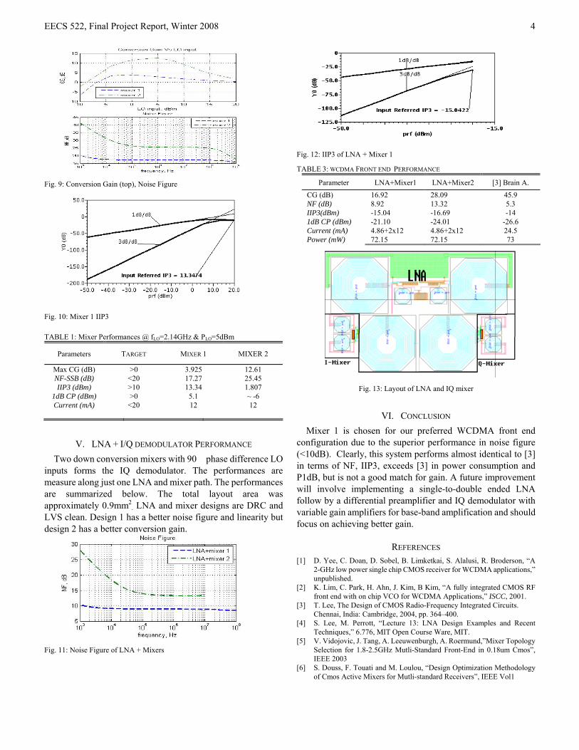
D. Mixer Performance Summary Mixer 1 has a better NF and linearity and Mixer 2 has a superior CG. The results are shown and summarized below.
EECS 522, Final Project Report, Winter 2008 4
Fig. 9: Conversion Gain (top), Noise Figure
Fig. 10: Mixer 1 IIP3
V. LNA + I/Q DEMODULATOR PERFORMANCE Two down conversion mixers with 90 phase difference LO
inputs forms the IQ demodulator. The performances are measure along just one LNA and mixer path. The performances are summarized below. The total layout area was approximately 0.9mm2
. LNA and mixer designs are DRC and LVS clean. Design 1 has a better noise figure and linearity but design 2 has a better conversion gain.
Fig. 11: Noise Figure of LNA + Mixers
Fig. 12: IIP3 of LNA + Mixer 1
TABLE 3: WCDMA FRONT END PERFORMANCE Parameter LNA+Mixer1 LNA+Mixer2 [3] Brain A.
CG (dB) 16.92 28.09 45.9 NF (dB) 8.92 13.32 5.3
IIP3(dBm) -15.04 -16.69 -14 1dB CP (dBm) -21.10 -24.01 -26.6 Current (mA) 4.86+2x12 4.86+2x12 24.5 Power (mW) 72.15 72.15 73
TABLE 1: Mixer Performances @ fLO=2.14GHz & PLO=5dBm
Parameters TARGET MIXER 1 MIXER 2
Max CG (dB) >0 3.925 12.61 NF-SSB (dB) <20 17.27 25.45
IIP3 (dBm) >10 13.34 1.807 1dB CP (dBm) >0 5.1 ~ -6 Current (mA) <20 12 12
Fig. 13: Layout of LNA and IQ mixer
VI. CONCLUSION Mixer 1 is chosen for our preferred WCDMA front end
configuration due to the superior performance in noise figure (<10dB). Clearly, this system performs almost identical to [3] in terms of NF, IIP3, exceeds [3] in power consumption and P1dB, but is not a good match for gain. A future improvement will involve implementing a single-to-double ended LNA follow by a differential preamplifier and IQ demodulator with variable gain amplifiers for base-band amplification and should focus on achieving better gain.
REFERENCES
[1] D. Yee, C. Doan, D. Sobel, B. Limketkai, S. Alalusi, R. Broderson, “A 2-GHz low power single chip CMOS receiver for WCDMA applications,” unpublished.
[2] K. Lim, C. Park, H. Ahn, J. Kim, B Kim, “A fully integrated CMOS RF front end with on chip VCO for WCDMA Applications,” ISCC, 2001.
[3] T. Lee, The Design of CMOS Radio-Frequency Integrated Circuits. Chennai, India: Cambridge, 2004, pp. 364–400.
[4] S. Lee, M. Perrott, “Lecture 13: LNA Design Examples and Recent Techniques,” 6.776, MIT Open Course Ware, MIT.
[5] V. Vidojovic, J. Tang, A. Leeuwenburgh, A. Roermund,”Mixer Topology Selection for 1.8-2.5GHz Mutli-Standard Front-End in 0.18um Cmos”, IEEE 2003
[6] S. Douss, F. Touati and M. Loulou, “Design Optimization Methodology of Cmos Active Mixers for Mutli-standard Receivers”, IEEE Vol1