
Topic 5 - Layout - Faculty of Engineering 5 - Layout... · Topic 5 Layout Design Peter Cheung ......
22
Topic 5 - 1 PYKC Nov-27-09 E4.20 Digital IC Design Topic 5 Layout Design Peter Cheung Department of Electrical & Electronic Engineering Imperial College London URL: www.ee.ic.ac.uk/pcheung/ E-mail: [email protected]
-
Upload
nguyendung -
Category
Documents
-
view
234 -
download
6
Transcript of Topic 5 - Layout - Faculty of Engineering 5 - Layout... · Topic 5 Layout Design Peter Cheung ......
Topic 5 - 1 PYKC Nov-27-09 E4.20 Digital IC Design
Topic 5
Layout Design
Peter Cheung Department of Electrical & Electronic Engineering
Imperial College London
URL: www.ee.ic.ac.uk/pcheung/ E-mail: [email protected]
Topic 5 - 2 PYKC Nov-27-09 E4.20 Digital IC Design
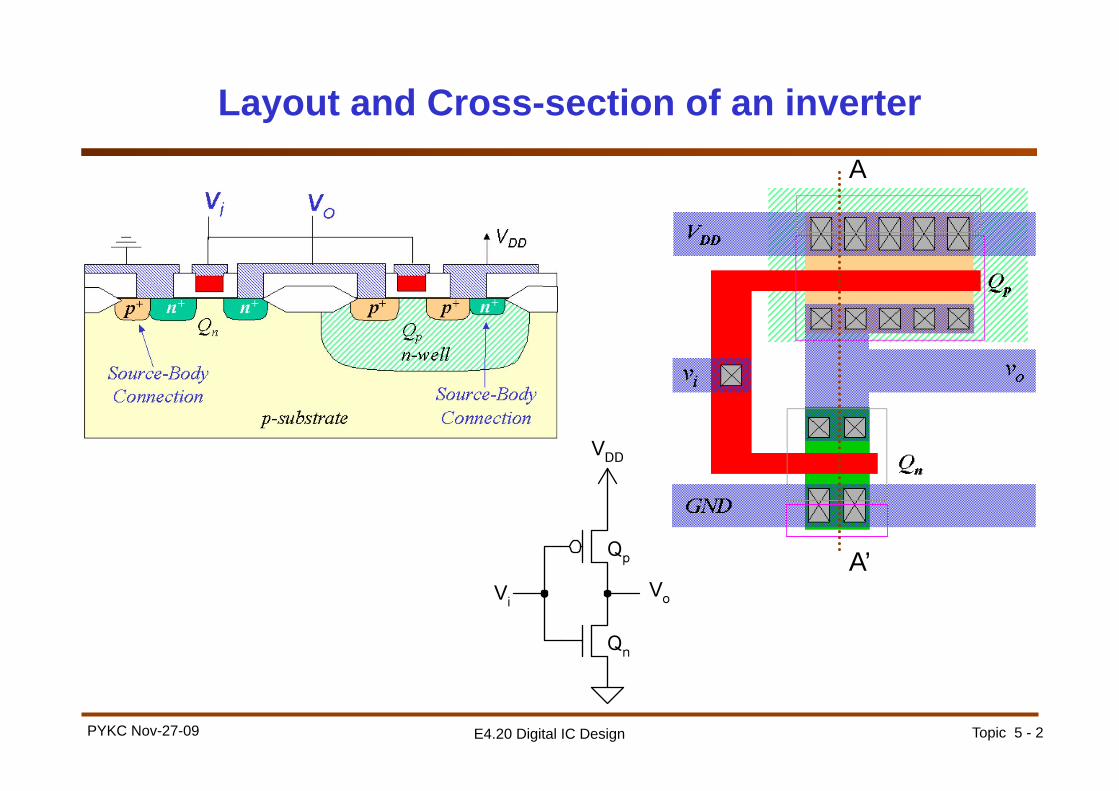
Layout and Cross-section of an inverter A
A’
Topic 5 - 3 PYKC Nov-27-09 E4.20 Digital IC Design
Layout & Fabrication
Fabrication uses a set of layers that are usually not exactly the same as the layout layers that the designer use because: • It is easy to combine some layers together - for example, all “active” layers
are diffusion layers (n+ and p+ diffusion) merged together. • Other layers used for fabrication can be deduced from other layers. For
example, the n-well region can be deduced from the p-type diffusion. • Therefore most layout CAD tools use mask layers that are more intuitive to
the layout designer, and map to the real mask later. CAD tools are used to generate the real mask layers for fabrication
• Generating the manufacturing mask data is called ‘tapeout’ • Some geometrical layout rules are created to make sure that this tapeout
process is possible. We will be using Steve Rubin’s Electric (version 8.05) as the main layout
editing tools. Install and run Electric, and bring out the User’s Manual. Read Chapter 2: Basic Editing. Complete Labs 1 & 2 (from course webpage).
Topic 5 - 4 PYKC Nov-27-09 E4.20 Digital IC Design
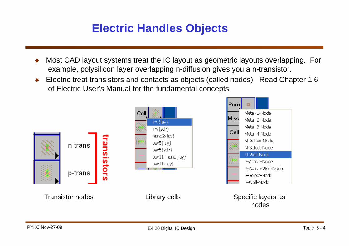
Electric Handles Objects
Most CAD layout systems treat the IC layout as geometric layouts overlapping. For example, polysilicon layer overlapping n-diffusion gives you a n-transistor.
Electric treat transistors and contacts as objects (called nodes). Read Chapter 1.6 of Electric User’s Manual for the fundamental concepts.
Transistor nodes Library cells Specific layers as nodes
Topic 5 - 5 PYKC Nov-27-09 E4.20 Digital IC Design
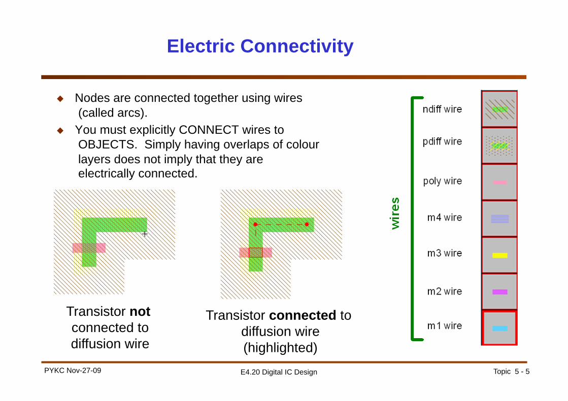
Electric Connectivity
Nodes are connected together using wires (called arcs).
You must explicitly CONNECT wires to OBJECTS. Simply having overlaps of colour layers does not imply that they are electrically connected.
Transistor not connected to diffusion wire
Transistor connected to diffusion wire (highlighted)
Topic 5 - 6 PYKC Nov-27-09 E4.20 Digital IC Design
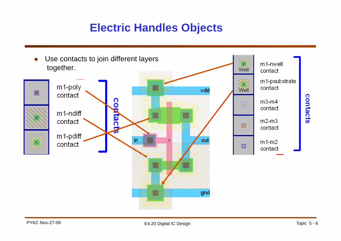
Electric Handles Objects
Use contacts to join different layers together.
Topic 5 - 7 PYKC Nov-27-09 E4.20 Digital IC Design
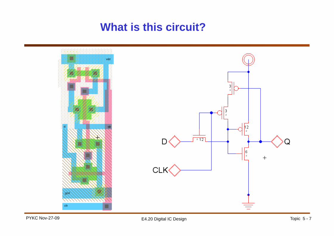
What is this circuit?
Topic 5 - 8 PYKC Nov-27-09 E4.20 Digital IC Design
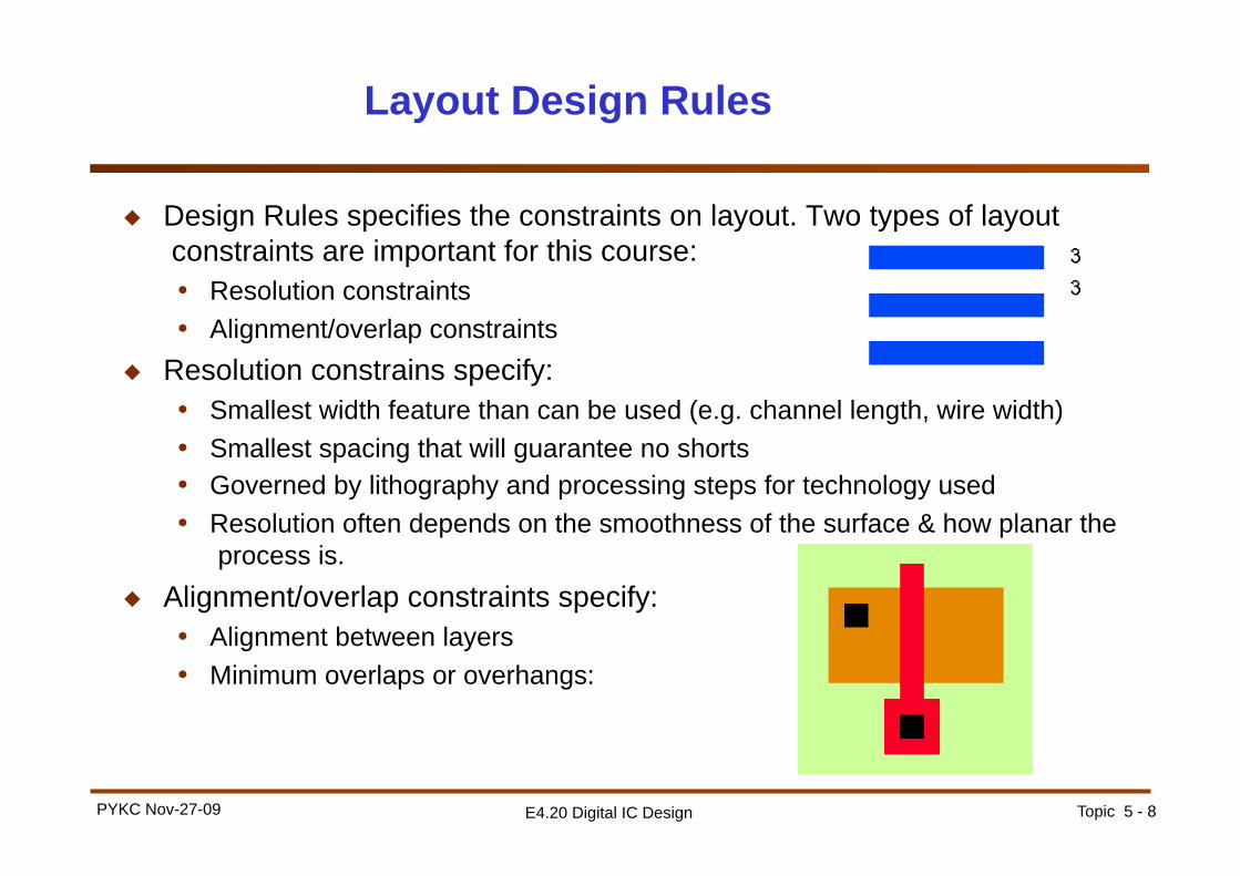
Layout Design Rules
Design Rules specifies the constraints on layout. Two types of layout constraints are important for this course: • Resolution constraints • Alignment/overlap constraints
Resolution constrains specify: • Smallest width feature than can be used (e.g. channel length, wire width) • Smallest spacing that will guarantee no shorts • Governed by lithography and processing steps for technology used • Resolution often depends on the smoothness of the surface & how planar the
process is. Alignment/overlap constraints specify:
• Alignment between layers • Minimum overlaps or overhangs:
Topic 5 - 9 PYKC Nov-27-09 E4.20 Digital IC Design
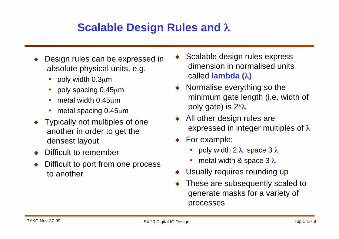
Scalable Design Rules and λ
Design rules can be expressed in absolute physical units, e.g. • poly width 0.3μm • poly spacing 0.45μm • metal width 0.45μm • metal spacing 0.45μm
Typically not multiples of one another in order to get the densest layout
Difficult to remember Difficult to port from one process
to another
Scalable design rules express dimension in normalised units called lambda (λ)
Normalise everything so the minimum gate length (i.e. width of poly gate) is 2*λ
All other design rules are expressed in integer multiples of λ
For example: • poly width 2 λ, space 3 λ • metal width & space 3 λ
Usually requires rounding up These are subsequently scaled to
generate masks for a variety of processes
Topic 5 - 10 PYKC Nov-27-09 E4.20 Digital IC Design
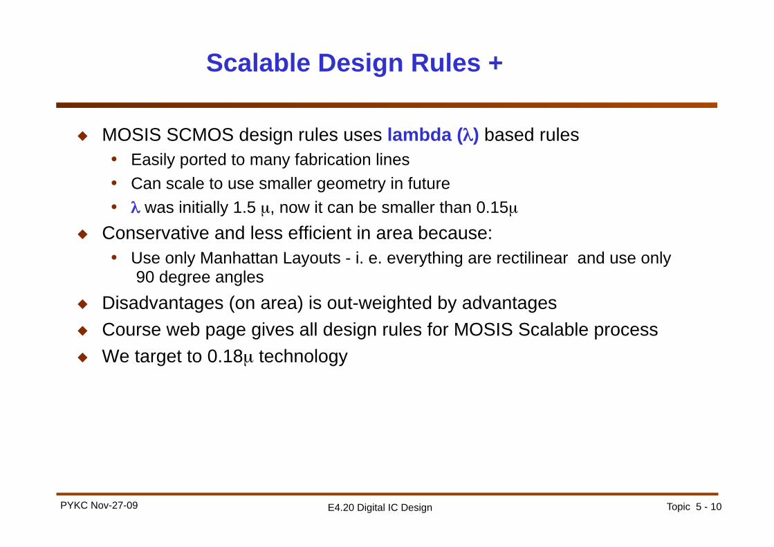
Scalable Design Rules +
MOSIS SCMOS design rules uses lambda (λ) based rules • Easily ported to many fabrication lines • Can scale to use smaller geometry in future • λ was initially 1.5 μ, now it can be smaller than 0.15μ
Conservative and less efficient in area because: • Use only Manhattan Layouts - i. e. everything are rectilinear and use only
90 degree angles Disadvantages (on area) is out-weighted by advantages Course web page gives all design rules for MOSIS Scalable process We target to 0.18μ technology
Topic 5 - 11 PYKC Nov-27-09 E4.20 Digital IC Design
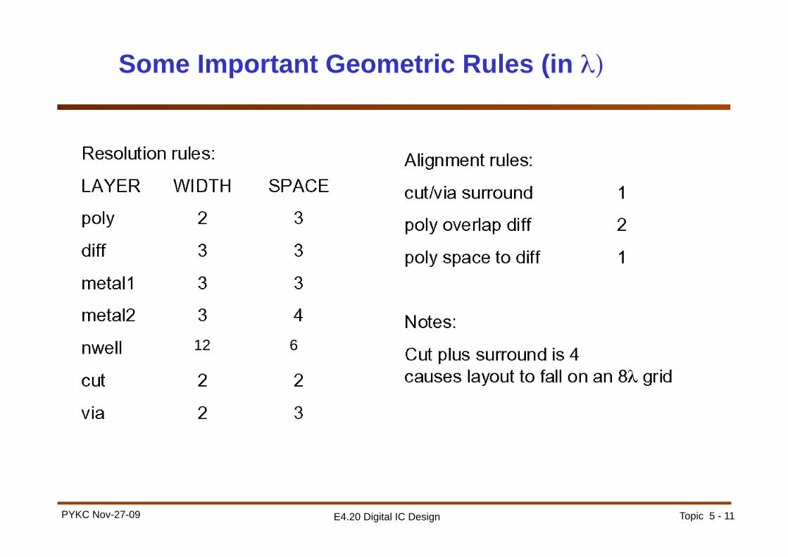
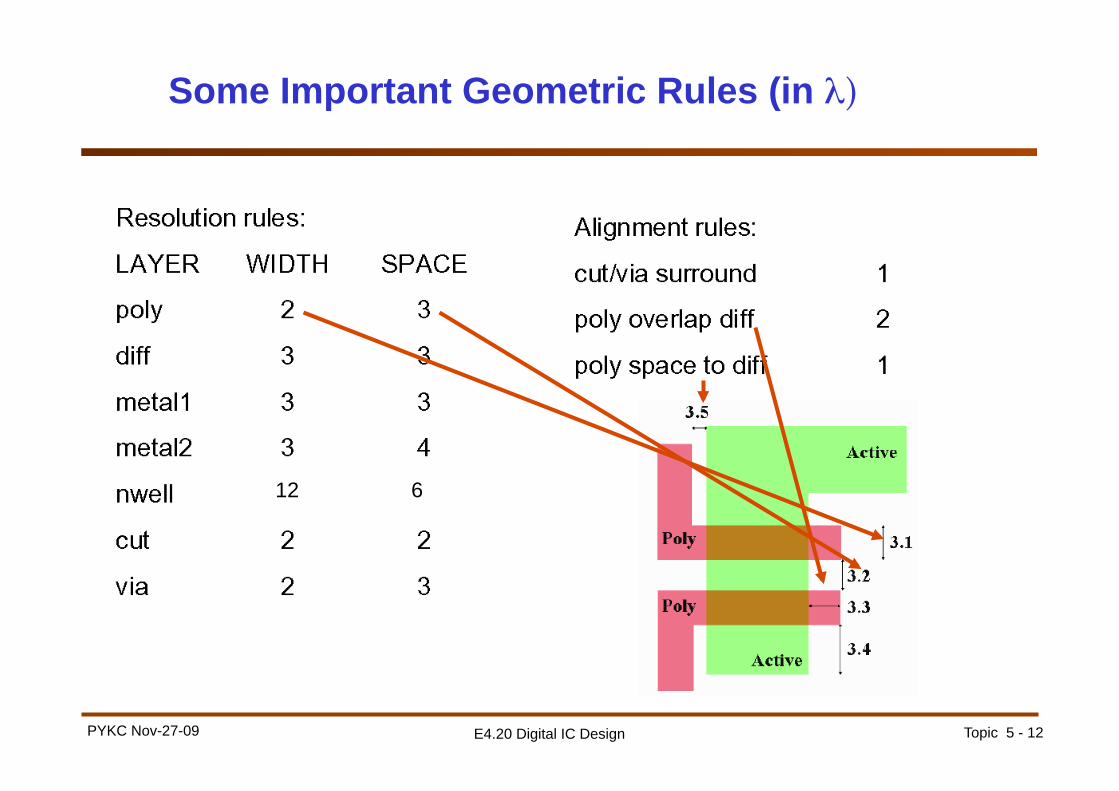
Some Important Geometric Rules (in λ)
12 6
Topic 5 - 12 PYKC Nov-27-09 E4.20 Digital IC Design
Some Important Geometric Rules (in λ)
12 6
Topic 5 - 13 PYKC Nov-27-09 E4.20 Digital IC Design
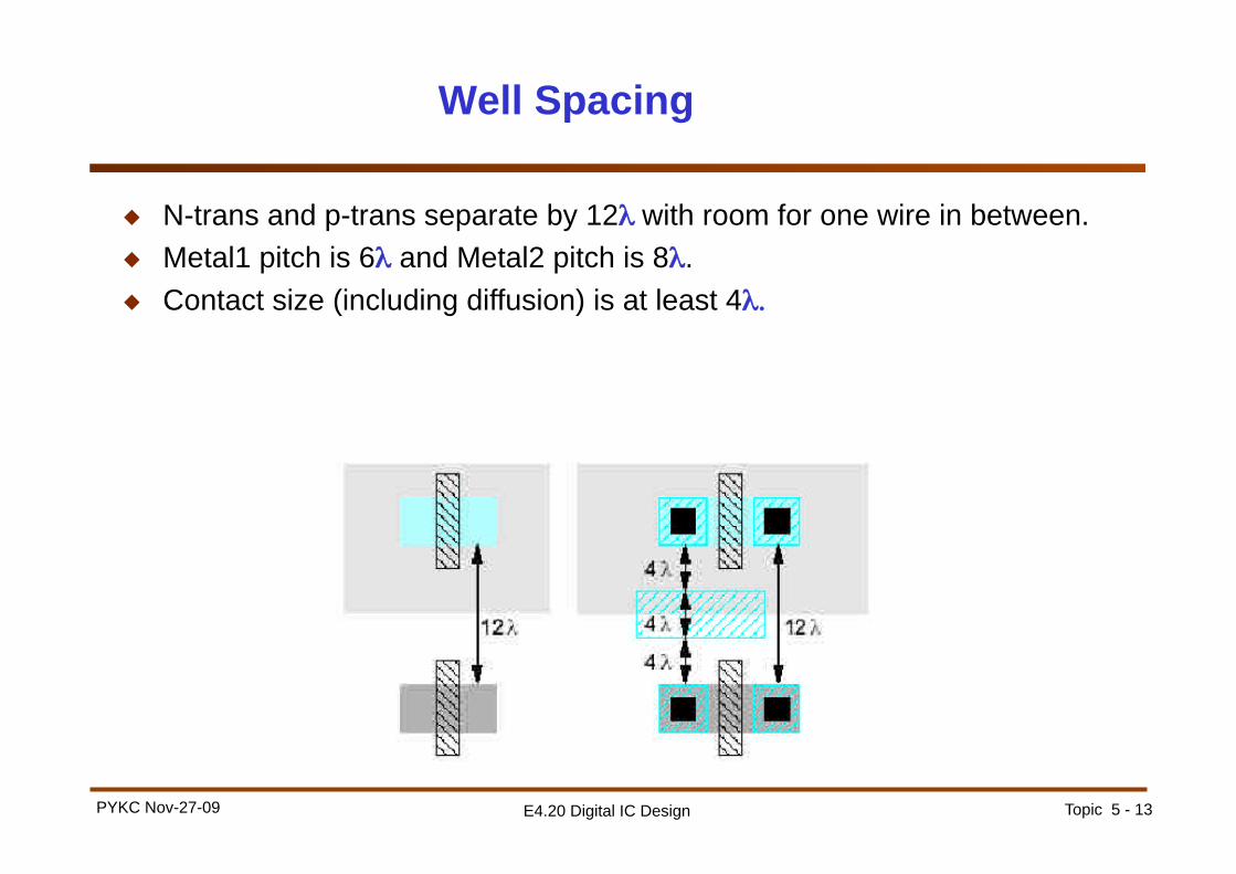
Well Spacing
N-trans and p-trans separate by 12λ with room for one wire in between. Metal1 pitch is 6λ and Metal2 pitch is 8λ. Contact size (including diffusion) is at least 4λ.
Topic 5 - 14 PYKC Nov-27-09 E4.20 Digital IC Design
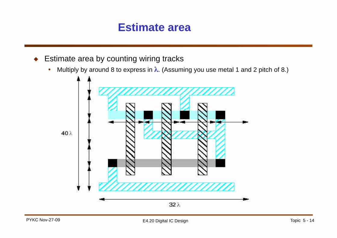
Estimate area
Estimate area by counting wiring tracks • Multiply by around 8 to express in λ. (Assuming you use metal 1 and 2 pitch of 8.)
Topic 5 - 15 PYKC Nov-27-09 E4.20 Digital IC Design
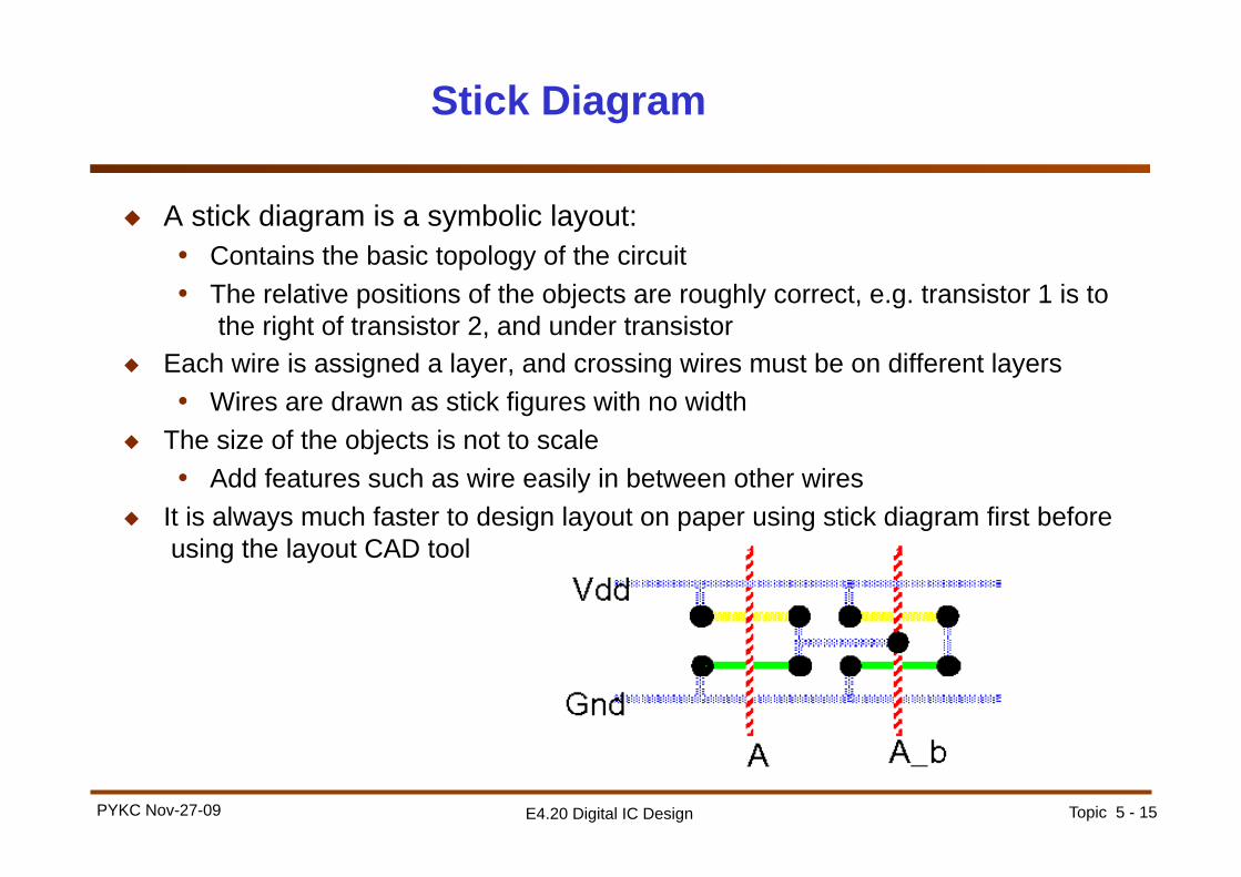
Stick Diagram
A stick diagram is a symbolic layout: • Contains the basic topology of the circuit • The relative positions of the objects are roughly correct, e.g. transistor 1 is to
the right of transistor 2, and under transistor Each wire is assigned a layer, and crossing wires must be on different layers
• Wires are drawn as stick figures with no width The size of the objects is not to scale
• Add features such as wire easily in between other wires It is always much faster to design layout on paper using stick diagram first before
using the layout CAD tool
Topic 5 - 16 PYKC Nov-27-09 E4.20 Digital IC Design
Layout issues
In CMOS there are two types of diffusion • ndiff (green) – Poly crossing ndiff makes nMOS transistors • pdiff (also green in Electric) – Poly crossing pdiff makes pMOS transistors
Be careful, ndiff and pdiff are different You can’t directly connect ndiff to pdiff
• Must connect ndiff to metal and then metal to pdiff Can’t get ndiff too close to pdiff because of wells Large spacing rule between ndiff and pdiff Need to group nMOS devices together and pMOS devices together
because of large spacing rule between ndiff and pdiff
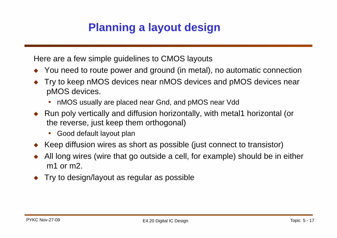
Topic 5 - 17 PYKC Nov-27-09 E4.20 Digital IC Design
Planning a layout design
Here are a few simple guidelines to CMOS layouts You need to route power and ground (in metal), no automatic connection Try to keep nMOS devices near nMOS devices and pMOS devices near
pMOS devices. • nMOS usually are placed near Gnd, and pMOS near Vdd
Run poly vertically and diffusion horizontally, with metal1 horizontal (or the reverse, just keep them orthogonal) • Good default layout plan
Keep diffusion wires as short as possible (just connect to transistor) All long wires (wire that go outside a cell, for example) should be in either
m1 or m2. Try to design/layout as regular as possible
Topic 5 - 18 PYKC Nov-27-09 E4.20 Digital IC Design
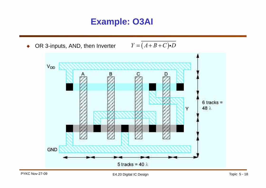
Example: O3AI
OR 3-inputs, AND, then Inverter
Topic 5 - 19 PYKC Nov-27-09 E4.20 Digital IC Design
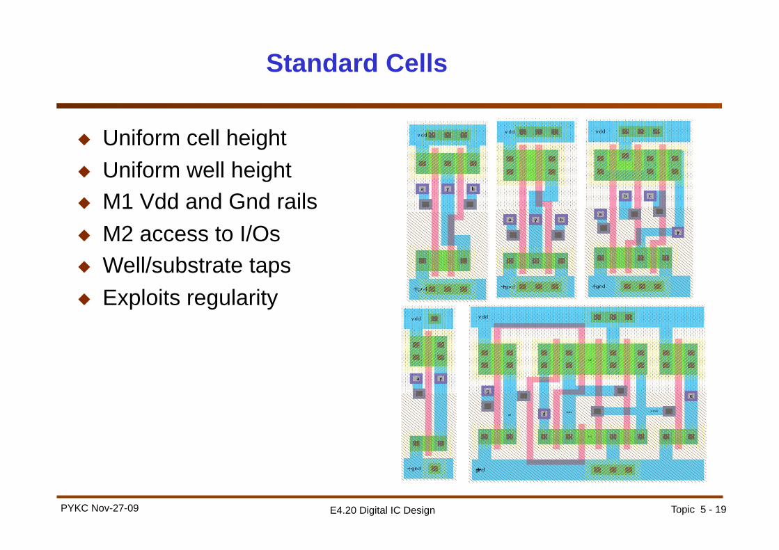
Standard Cells
Uniform cell height Uniform well height M1 Vdd and Gnd rails M2 access to I/Os Well/substrate taps Exploits regularity
Topic 5 - 20 PYKC Nov-27-09 E4.20 Digital IC Design
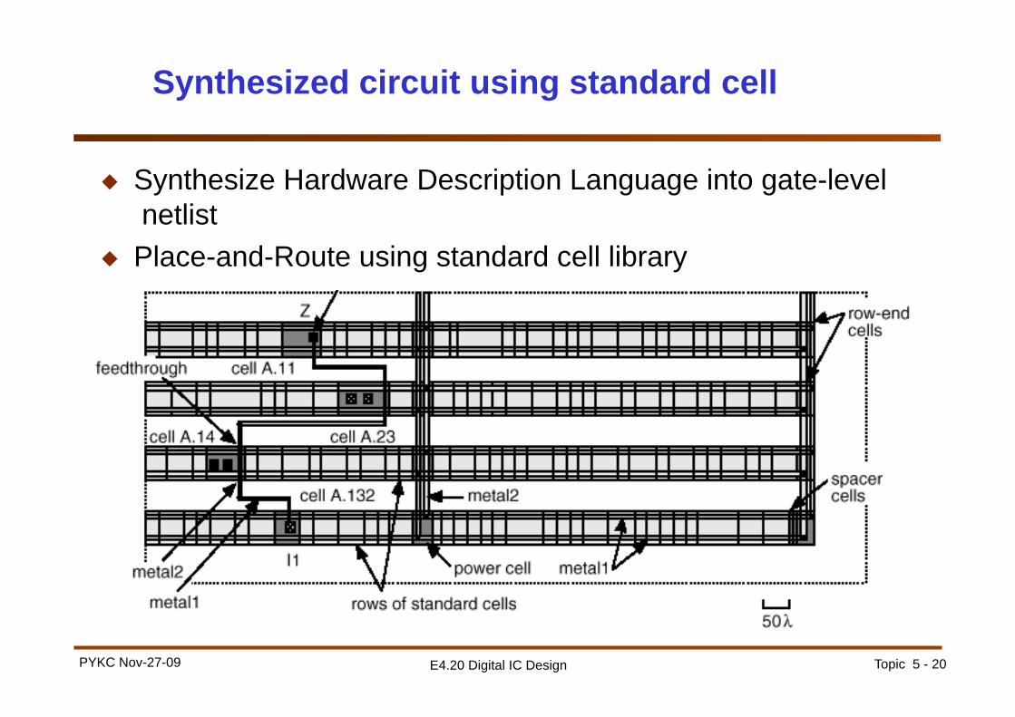
Synthesized circuit using standard cell
Synthesize Hardware Description Language into gate-level netlist
Place-and-Route using standard cell library
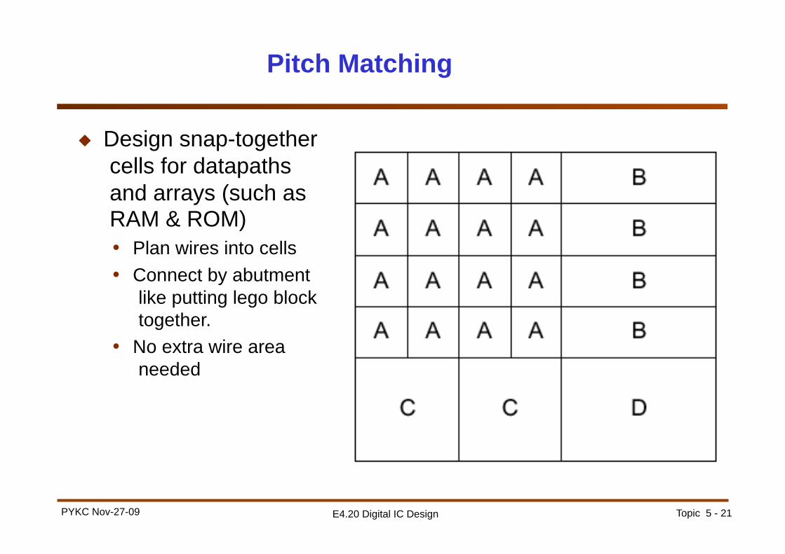
Topic 5 - 21 PYKC Nov-27-09 E4.20 Digital IC Design
Pitch Matching
Design snap-together cells for datapaths and arrays (such as RAM & ROM) • Plan wires into cells • Connect by abutment
like putting lego block together.
• No extra wire area needed
Topic 5 - 22 PYKC Nov-27-09 E4.20 Digital IC Design
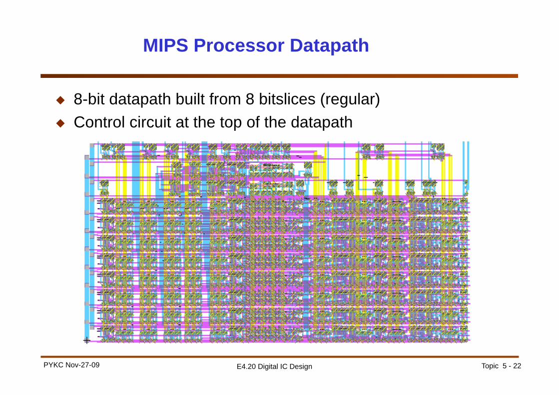
MIPS Processor Datapath
8-bit datapath built from 8 bitslices (regular) Control circuit at the top of the datapath


![Topic 7 Revision [143 marks]](https://static.fdocument.org/doc/165x107/616a52ca11a7b741a3513f24/topic-7-revision-143-marks.jpg)