SRM Nagar, Kattankulathur-603 203 - | Anna...
13
Page 1 of 13 VALLIAMMAI ENGINEERING COLLEGE SRM Nagar, Kattankulathur-603 203 DEPARTMENT OF ELECTRONICS AND COMMUNICATION ENGINEERING EC6302 DIGITAL ELECTRONICS YEAR / SEMESTER: II / III ACADEMIC YEAR: 2015-2016 (ODD SEMESTER) QUESTION BANK www.studentsfocus.com
Transcript of SRM Nagar, Kattankulathur-603 203 - | Anna...
Page 1 of 13
VALLIAMMAI ENGINEERING COLLEGE
SRM Nagar, Kattankulathur-603 203
DEPARTMENT OF ELECTRONICS AND COMMUNICATION ENGINEERING
EC6302 DIGITAL ELECTRONICS
YEAR / SEMESTER: II / III
ACADEMIC YEAR: 2015-2016 (ODD SEMESTER)
QUESTION BANK
www.studentsfocus.com
Page 2 of 13
UNIT –I
MINIMIZATION TECHNIQUES AND LOGIC GATES
Part – A
1. Apply De-Morgan’s theorem to simplify A+BC.
2. Define the term prime implicants and Essential prime implicants.
3. Draw the XOR logic using only NAND gates.
4. Implement the following Boolean function with NOR – NOR logic
F = Π (0, 2, 4,5,6)
5. Express the switching function f (ABC) = B in terms of minterm.
6. Define minterm & Maxterm. Give examples.
7. Simplify the given Boolean Expression F= x’+xy+xz’+xy’z’.
8. Prove that the logical sum of all minterms of a Boolean function of 2 variables is 1.
9. Show that a positive logic NAND gate is a negative logic NOR gate.
10. If A & B are Boolean variables and if A=1 & A+B=0, Find B?
11. Realize F = A’B+AB’ using minimum universal gates.
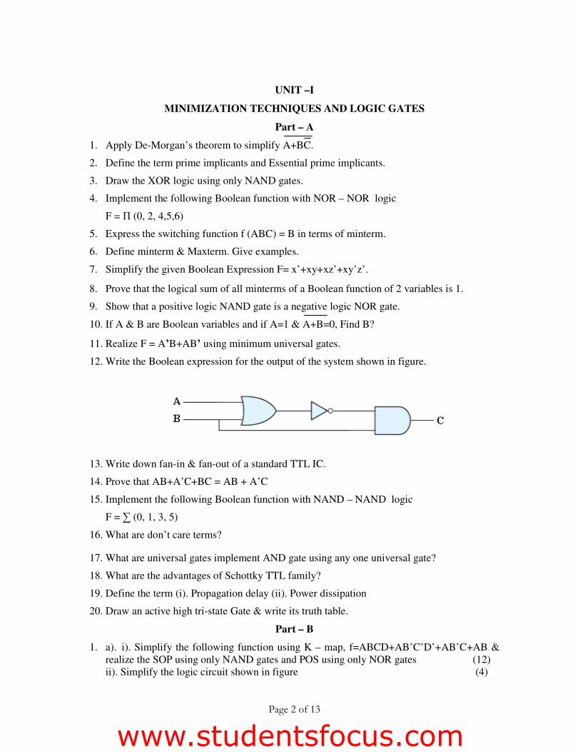
12. Write the Boolean expression for the output of the system shown in figure.
13. Write down fan-in & fan-out of a standard TTL IC.
14. Prove that AB+A’C+BC = AB + A’C
15. Implement the following Boolean function with NAND – NAND logic
F = ∑ (0, 1, 3, 5)
16. What are don’t care terms?
17. What are universal gates implement AND gate using any one universal gate?
18. What are the advantages of Schottky TTL family?
19. Define the term (i). Propagation delay (ii). Power dissipation
20. Draw an active high tri-state Gate & write its truth table.
Part – B
1. a). i). Simplify the following function using K – map, f=ABCD+AB’C’D’+AB’C+AB & realize the SOP using only NAND gates and POS using only NOR gates (12)
ii). Simplify the logic circuit shown in figure (4)
www.studentsfocus.com
Page 3 of 13
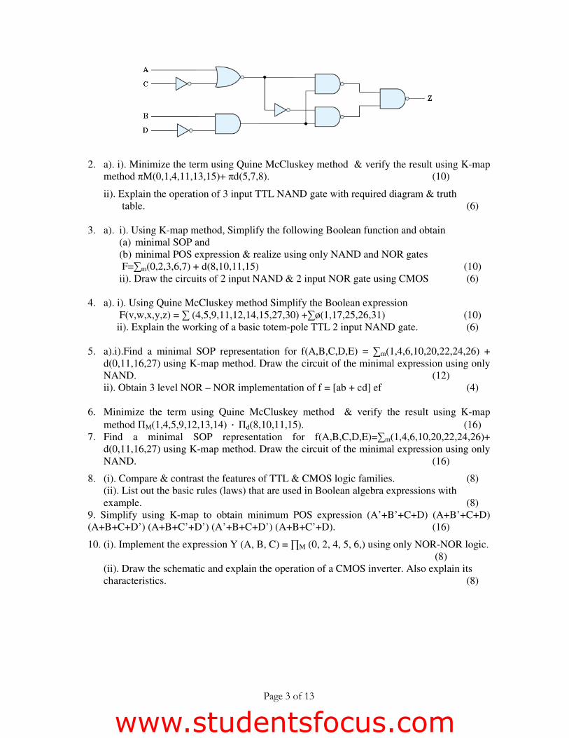
2. a). i). Minimize the term using Quine McCluskey method & verify the result using K-map
method πM(0,1,4,11,13,15)+ πd(5,7,8). (10)
ii). Explain the operation of 3 input TTL NAND gate with required diagram & truth table. (6) 3. a). i). Using K-map method, Simplify the following Boolean function and obtain
(a) minimal SOP and (b) minimal POS expression & realize using only NAND and NOR gates F=∑m(0,2,3,6,7) + d(8,10,11,15) (10) ii). Draw the circuits of 2 input NAND & 2 input NOR gate using CMOS (6)
4. a). i). Using Quine McCluskey method Simplify the Boolean expression
F(v,w,x,y,z) = ∑ (4,5,9,11,12,14,15,27,30) +∑ø(1,17,25,26,31) (10) ii). Explain the working of a basic totem-pole TTL 2 input NAND gate. (6) 5. a).i).Find a minimal SOP representation for f(A,B,C,D,E) = ∑m(1,4,6,10,20,22,24,26) +
d(0,11,16,27) using K-map method. Draw the circuit of the minimal expression using only NAND. (12) ii). Obtain 3 level NOR – NOR implementation of f = [ab + cd] ef (4)
6. Minimize the term using Quine McCluskey method & verify the result using K-map
method ΠM(1,4,5,9,12,13,14) · Πd(8,10,11,15). (16) 7. Find a minimal SOP representation for f(A,B,C,D,E)=∑m(1,4,6,10,20,22,24,26)+
d(0,11,16,27) using K-map method. Draw the circuit of the minimal expression using only NAND. (16)
8. (i). Compare & contrast the features of TTL & CMOS logic families. (8) (ii). List out the basic rules (laws) that are used in Boolean algebra expressions with example. (8)
9. Simplify using K-map to obtain minimum POS expression (A’+B’+C+D) (A+B’+C+D) (A+B+C+D’) (A+B+C’+D’) (A’+B+C+D’) (A+B+C’+D). (16)
10. (i). Implement the expression Y (A, B, C) = ∏M (0, 2, 4, 5, 6,) using only NOR-NOR logic. (8) (ii). Draw the schematic and explain the operation of a CMOS inverter. Also explain its characteristics. (8)
www.studentsfocus.com
Page 4 of 13
UNIT –II
COMBINATIONAL CIRCUITS
Part – A
1. What is combinational circuit? Give examples.
2. Draw the block diagram of n-bit parallel adder
3. Write an expression for borrow and difference in a full Subtractor circuit.
4. Differentiate a decoder from a Demultiplexer.
5. Design Half – adder using only NAND gates.
6. What is code converter? List their types.
7. Draw a logic diagram of 1 to 4 data distributor
8. Express Gray code 10111into binary numbers.
9. Implement full adder using multiplexer.
10. Draw the block diagram of a 2’s complement 4 – bit adder/ Subtractor.
11. Write the function table and logic diagram of a 4:1 data selector.
12. Implement the following function using suitable multiplexer F= Σm(0,2,5,7)
13. Relate carry generate, carry propagate, sum and carry-out of a carry look ahead adder.
14. Design a single bit magnitude comparator to compare two words A and B.
15. What is priority encoder?
16. Design a three bit even parity generator.
17. Draw the logic diagram of a serial adder.
18. Design a half subtractor combinational circuit to produce the outputs Difference and
Borrow.
19. Draw the logic diagram of a 2 bit multiplier.
20. Suggest a solution to overcome the limitation on the speed of an adder.
Part – B
1. (i). Implement the following function using suitable multiplexer F (A, B, C, D) = Σ(1, 3, 4,
11, 12, 13, 14 , 15 ) (8)
(ii). Draw the logic diagram of a 2-bit by 2-bit binary multiplier and explain its operation. (8)
2. Draw the block schematic of Magnitude comparator and explain its operation (16)
3. Draw & explain the block diagram of a 4-bit parallel adder / Subtractor (16)
4. (i) Design & implement the conversion circuits for BCD to Excess – 3 code. (10)
(ii) Implement full subtractor using Demultiplexer. (6)
www.studentsfocus.com
Page 5 of 13
5. Design an Excess – 3 to BCD code converter. Uses don’t care (16)
6. (i). Implement full adder using decoder. (6)
(ii).Realize F(w, x, y, z)= Σ (1,4,6,7,8,9,10,11,15) using 8 to 1 Mux (10)
7. Explain the operation of carry look ahead adder with neat diagram (16)
8. (i). Draw and explain the BCD adder circuit. (10)
(ii). Design a seven segment decoder circuit to display the numbers from 0 to 3. (6)
9. (i). Draw the logic diagram of BCD to Decimal decoder and explain its operations. (10)
(ii).Explain even parity checker and generator. (6)
10. Draw & explain the block diagram of a 4-bit serial adder to add contents of two registers.
(16)
UNIT –III
SEQUENTIAL CIRCUITS
Part – A
1. Compare Asynchronous and Synchronous sequential logic.
2. Draw the state diagram and characteristics equation of a D FF.
3. What is latch? What is the difference between latch and flip flop?
4. Realize T Flip Flop using SR Flip Flop
5. How does the JK FF differ from an SR FF in its basic equation?
6. Define Synchronous counter.
7. Define Setup and Hold time.
8. What is the condition on JK FF to work as D FF?
9. What is race around condition? How do you eliminate it?
10. Mention any two differences between the edge triggering and level triggering.
11. Draw the state diagram of MOD -10 counters.
12. What is sequential circuit? Give some example.
13. Draw a NAND based logic diagram of Master Slave JK FF.
14. Convert Transparent flip flop into a JK flip flop.
15. Differentiate Asynchronous and Modulus counter
16. Define the terms State table and State Assignment.
17. What is meant by programmable counter? Mention its applications.
18. Draw the state table and excitation table of T flip flop.
19. How many Flip Flops are required to build a binary counter that counts from 0 to 1023.
20. Design a 3 bit ring counter and find the mod of a designed counter.
Part – B
www.studentsfocus.com
Page 6 of 13
1. i). Design and explain the working of an 4-bit Parallel counter (8)
ii). Design and working of a BCD ripple counter with timing diagram. (8)
2. i).Design a 3 bit synchronous counter which counts in the sequence 000, 001, 011,
010,100, 110, (repeat) 000 …using D flip flop. (10)
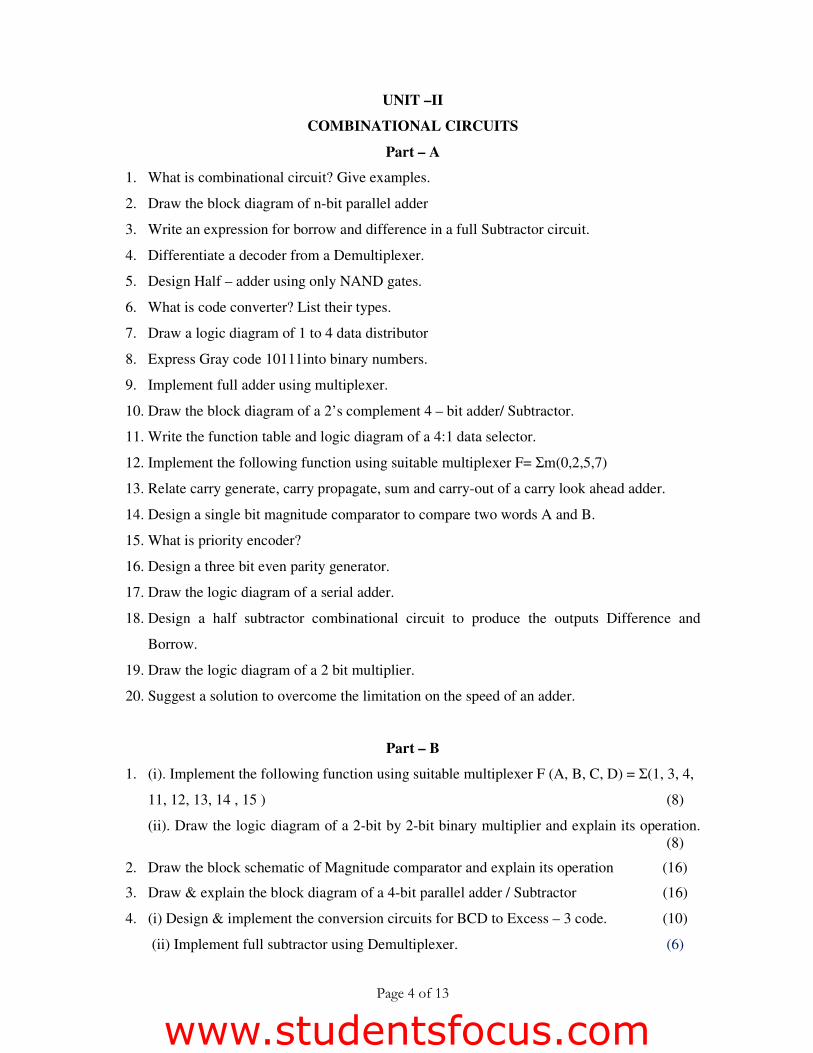
ii).Analyze the logic diagram and draw the state diagram for the given logic. (6)
3. i).Design and explain the working of an 4-bit Up/Down ripple counter (8)
ii). Design and working of a synchronous MOD- 5 counter. (8)
4. i).Design a synchronous counter with states 0, 1, 2, 3, 0, 1, .... using JK flip flop. (8)
ii).Construct a JK FF using a D FF, a 2:1 Multiplexer and an inverter. (8)
5. i).Design and explain the working of an 4-bit Up/Down Parallel counter. (10)
ii). Realize JK Flip Flop using SR Flip Flop (6)
6. (i).Explain the operation of universal shift register with neat block diagram. (8)
(ii). Explain the working Master/Slave JK FF (8)
7. i). Draw the logic diagram for a 5- bit serial load shift register using D FF & explain. (10)
ii). Write notes on state minimization. (6)
8. Draw a 4-bit SISO SIPO, PIPO and PISO shift register and draw its waveforms (16)
9. i). Draw an asynchronous decade counter & explain its operation with neat waveforms.(8)
ii). Design a 3-bit binary counter using T FF that has a repeated sequence of 6 states. 000-
001-010-011-100-101-110. Give the state table, state diagram & logic diagram. (8)
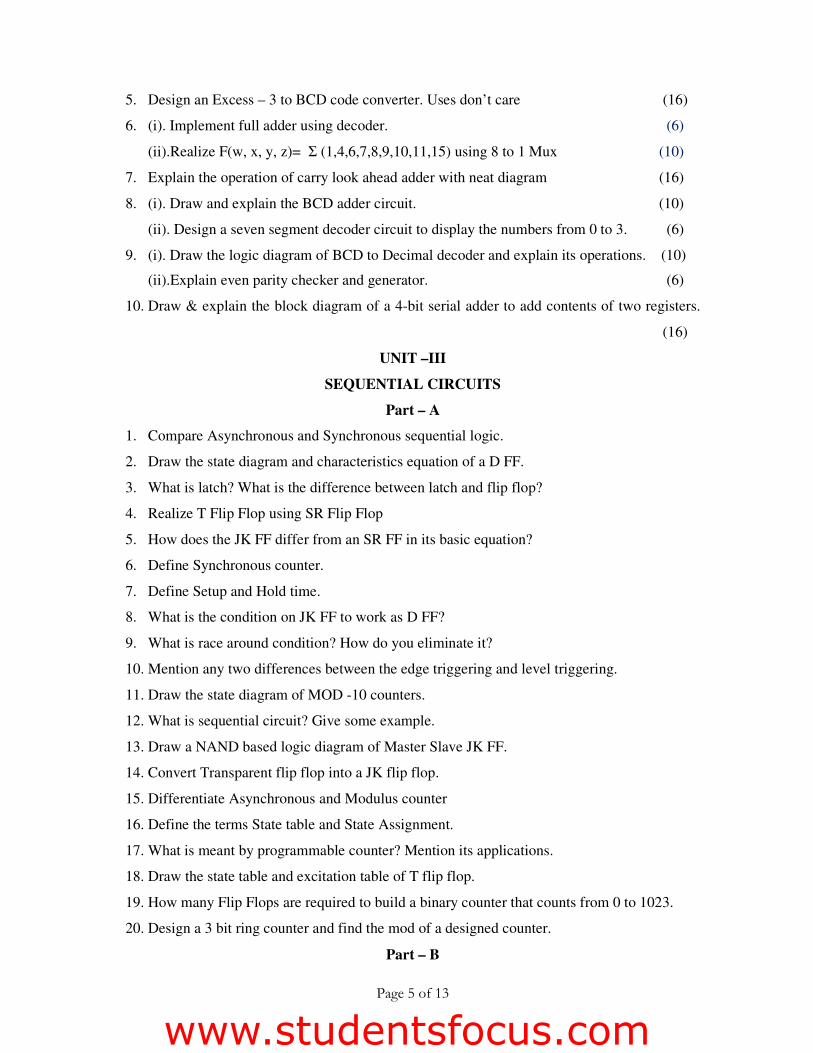
10. Sequential circuit has three flip flops A, B, and C; one input x_in ; and one output
y_out. The state diagram is shown in below figure. The circuit is to be designed by
treating the unused states as don’t care conditions. Analyze the circuit obtain from
the design to determine the effect of the unused states. Use T flip flops in the design.
(16)
www.studentsfocus.com
Page 7 of 13
UNIT –IV
MEMORY DEVICES
Part – A
1. How the memories are classified.
2. What is an EPROM?
3. Compare and contrast static RAM and dynamic RAM
4. What is PLD? List their types.
5. Explain write operation with an example.
6. Distinguish between PAL and PLA.
7. Which memory is called volatile? Why?
8. Write the advantages of EPROM over a PROM.
9. Compare the features of PROM, PAL and PLA
10. What is access time and cycle time of a memory?
11. What is PLA? How does it differ from PAL and GAL?
12. What is memory decoding?
13. Implement the Exclusive-OR function using PROM
14. Write the advantages of E2PROM over an EPROM.
15. Implement the function F1=∑ (0, 1, 2, 5, 7) and F2 = ∑ (1, 2, 4, 6) using PROM.
16. Draw the static and dynamic RAM cells.
17. Implement a 2-bit multiplier using ROM.
18. What is meant by memory expansion? Mention its limit.
www.studentsfocus.com
Page 8 of 13
19. Compare PLD’s with FPGA.
20. Draw the equivalent logic circuit of a binary memory cell that stores one bit of information.
Part – B
1. i). Give the classification of semiconductor memories (8)
ii). Implement the following function using PLA F1=∑ (2, 4, 5, 10, 12, 13, 14) and
F2 = ∑ (2, 9, 10, 11, 13, 14, 15). (8)
2. i). Write short note on RAM, types of ROMs (10)
ii). Implement the following function using PLA F1=∑ (0, 1, 2, 4) and
F2 = ∑ (0, 5, 6, 7). (6)
3. i). Realize the following function using PAL
F1(x, y, z) = ∑ (1, 2, 4, 5, 7). And
F2(x, y, z) = ∑ (0, 1, 3, 5, 7) (8)
ii). Write a note on FPGA with neat diagram. (8)
4. i). Explain read cycle and write cycle timing parameter with the help of timing
diagram. (10)
ii). A combinational circuit is defined as the function F1 = AB’C’+AB’C+ABC and F2
= A’BC+AB’C+ABC. Implement the digital circuit with a PLA having 3 inputs, 3 product
terms and 2 outputs. (6)
5. i).Write short notes on PLD, types of PLDs. (8)
ii). Implement the following Boolean function using 3×4×2 PLA, F1(x, y, z) = ∑ (0, 1,
3, 5) and F2(x, y, z) = ∑ (3, 5, 7) (8)
6. i).Design a combinational circuit using ROM. The circuit accepts a three bit number
and outputs a binary number equal to the square of the input number. (8)
ii). Describe the RAM organization. (8)
7. i). Draw a PLA circuit to implement the function F1 = A’B + AC’,
F2 = (AC + AB + BC)’ (8)
ii). Write short notes on EPROM and EEPROM. (8)
8. i). Realize the following function using PLA F (w, x, y, z) = Π (0, 3, 5, 7, 12, 15)
+ d (2, 9). (8)
ii). Implement Binary to Gray code converter using PROM devices (8)
www.studentsfocus.com
Page 9 of 13
9. Implement the following Boolean functions using 4 × 3 × 4 PAL (16)
i. W(A, B, C, D) = ∑ (0, 2, 6, 7, 8, 9, 12, 13)
ii. X (A, B, C, D) = ∑ (0, 2, 6, 7, 8, 9, 12, 13, 14).
iii. Y(A, B, C, D) = ∑ ( 2, 3, 8, 9, 10, 12, 13)
iv. Z(A, B, C, D) = ∑ (1, 3, 4, 6, 9, 12, 14)
10. i). Explain the principle of operation of Bipolar SRAM cell. (8)
ii). How can one make 64X8 ROM using 32X4 ROMs? Draw such a circuit & explain.
(8)
UNIT –V
SYNCHRONOUS AND ASYNCHRONOUS SEQUENTIAL CIRCUITS
Part – A
1. Differentiate synchronous and asynchronous sequential circuits?
2. What are the two types of Asynchronous sequential circuits?
3. Differentiate Moore machine and Mealy machine.
4. Define flow table and primitive flow table.
5. Write a Verilog HDL model of a full subtractor circuit.
6. Define state table and state assignment.
7. Draw the basic building blocks of an Algorithmic State Machine chart?
8. Differentiate stable and unstable state.
9. Write a Verilog behavioral model of a Transparent flip flop with reset input.
10. Draw block diagram for Moore and Mealy model.
11. Define the terms race and critical race.
12. What is a state diagram? Give an example
13. Write a Verilog code for 4-to-2 Encoder using gate level model.
14. What are Hazards? How it can be avoided?
15. Compare the ASM chart with a conventional flow chart.
16. Differentiate fundamental mode and pulse mode asynchronous sequential circuits.
17. Design a 3 input NAND gate using Verilog.
18. What is the cause for essential Hazard?
19. Write a Verilog model of 4:1 multiplexer circuit.
20. Write analysis procedure of synchronous sequential circuits.
www.studentsfocus.com
Page 10 of 13
Part – B
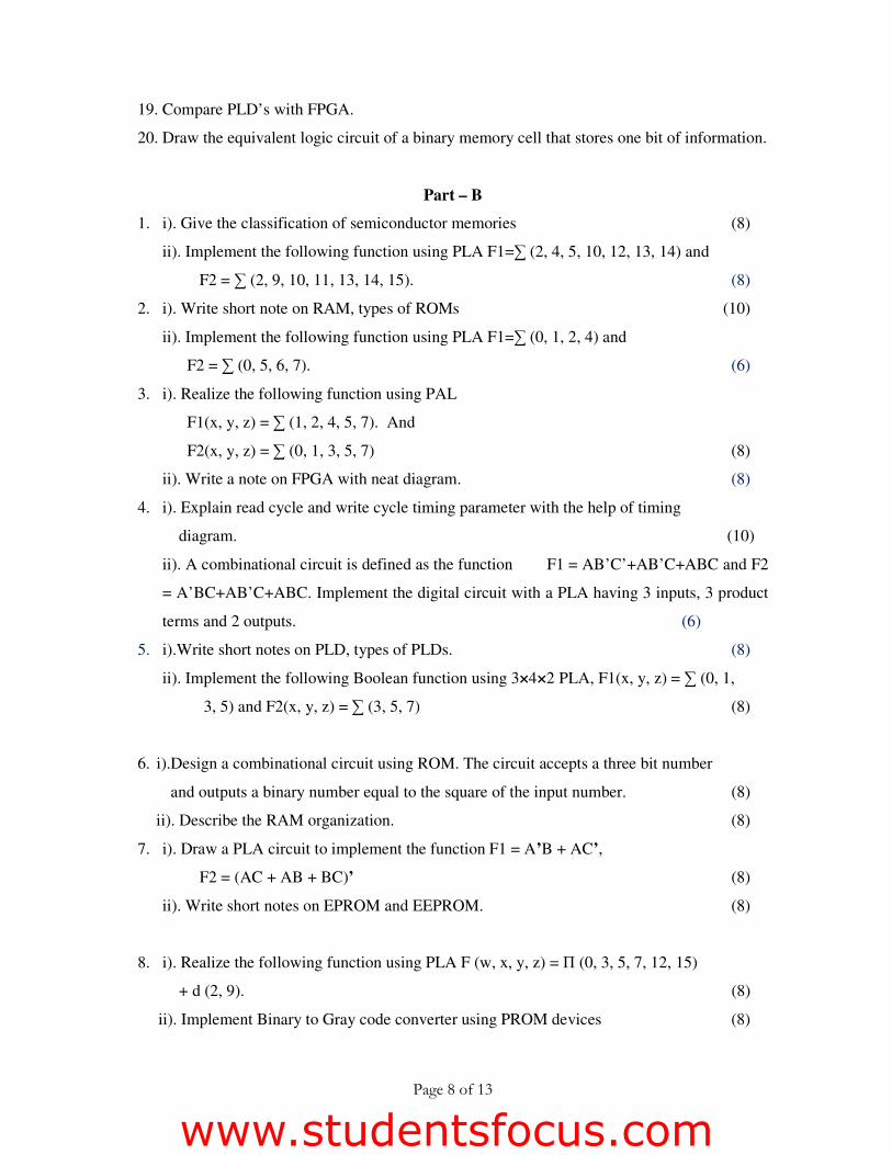
1. Design a clocked synchronous sequential logic circuit using JK flip flops for the
following state diagram. Use state reduction if possible. (16)
2. What is a Hazard? What are the types of hazards? Check whether the following
circuit contains a hazard or not Y = x1x2 + x2′x3 2If the hazard is present,
demonstrate its removal (16)
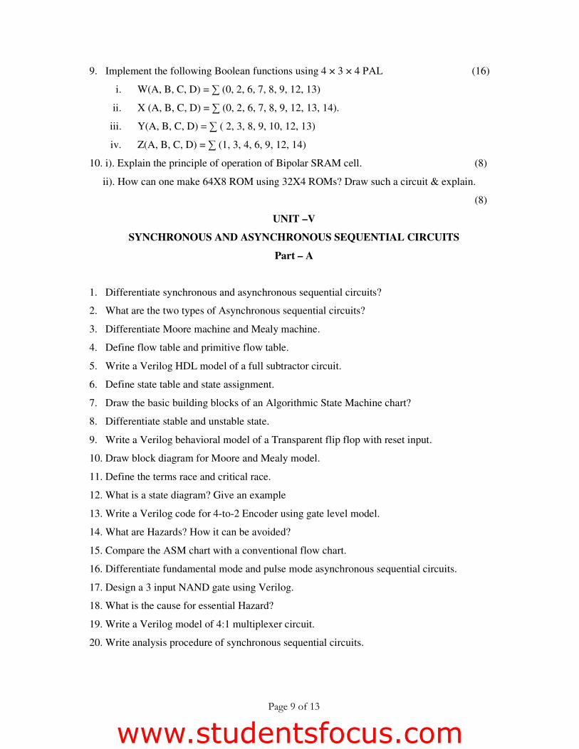
3. Design a clocked sequential machine using JK flip flops for the state diagram shown
in figure. Use state reduction if possible and make proper state assignment. (16)
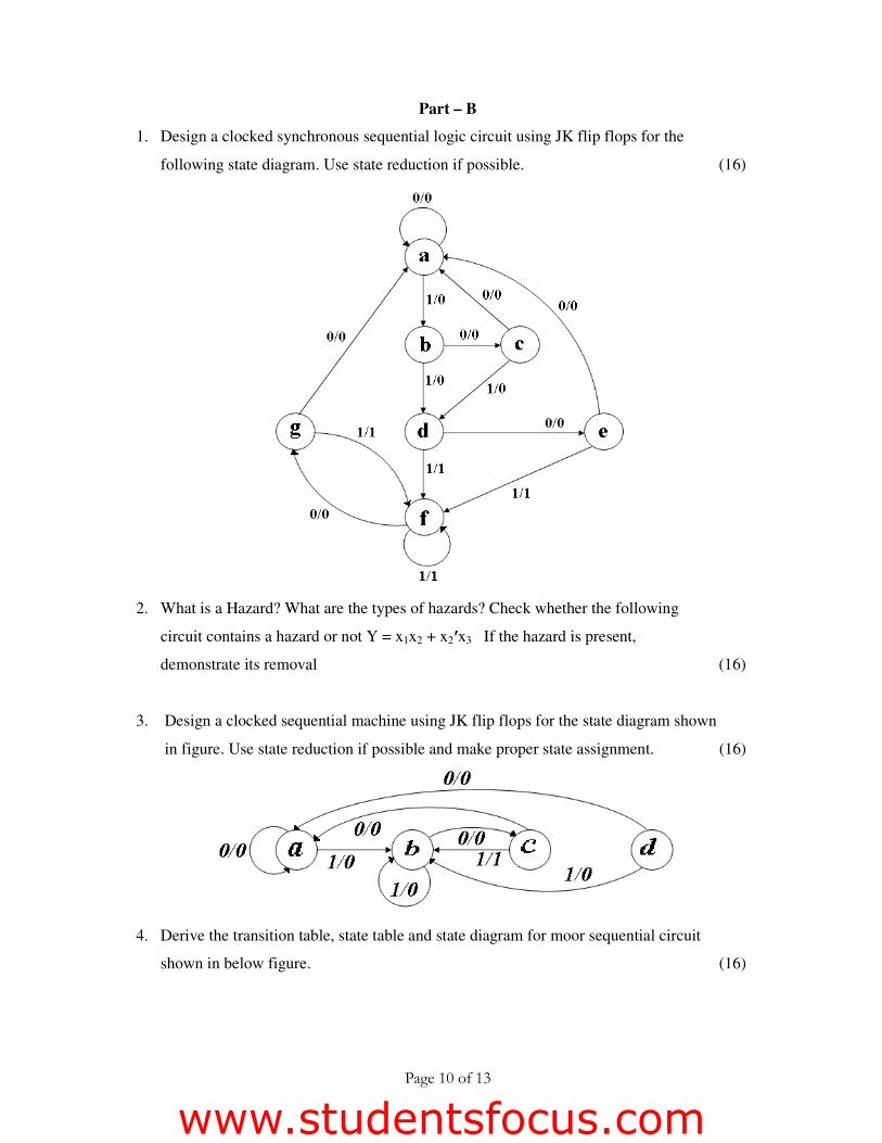
4. Derive the transition table, state table and state diagram for moor sequential circuit
shown in below figure. (16)
www.studentsfocus.com
Page 11 of 13
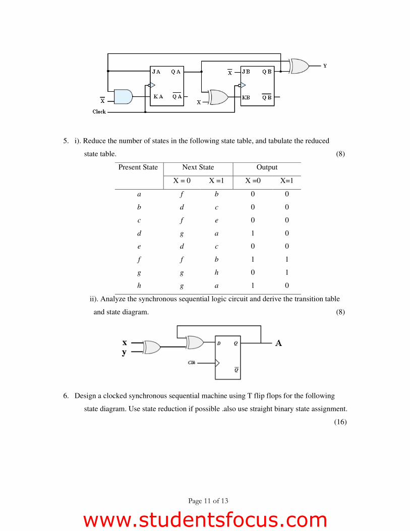
5. i). Reduce the number of states in the following state table, and tabulate the reduced
state table. (8)
Present State Next State Output
X = 0 X =1 X =0 X=1
a f b 0 0
b d c 0 0
c f e 0 0
d g a 1 0
e d c 0 0
f f b 1 1
g g h 0 1
h g a 1 0
ii). Analyze the synchronous sequential logic circuit and derive the transition table
and state diagram. (8)
6. Design a clocked synchronous sequential machine using T flip flops for the following
state diagram. Use state reduction if possible .also use straight binary state assignment.
(16)
www.studentsfocus.com
Page 12 of 13
7. i).What is hazards? Give hazard free realization for the following Boolean function.
F(A, B, C, D) = ∑m(0, 2, 6, 7, 8, 10, 12) (10)
ii).Differentiate Moore and Mealy machines with block diagram (6)
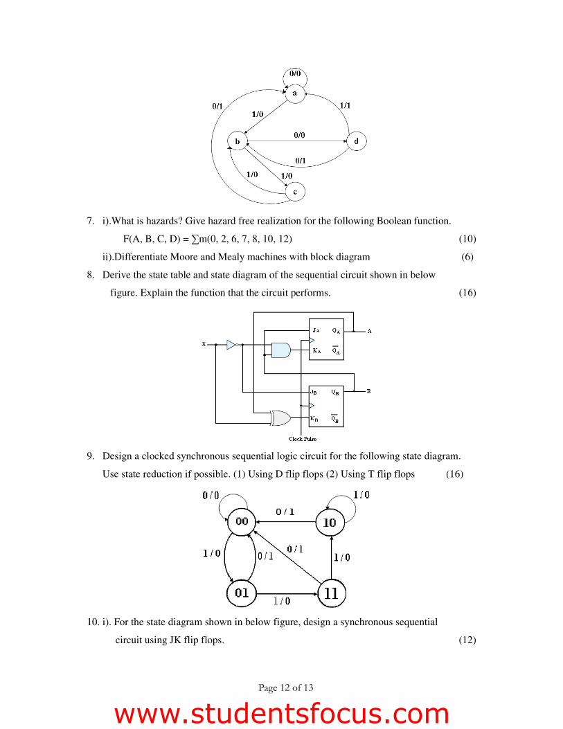
8. Derive the state table and state diagram of the sequential circuit shown in below
figure. Explain the function that the circuit performs. (16)
9. Design a clocked synchronous sequential logic circuit for the following state diagram.
Use state reduction if possible. (1) Using D flip flops (2) Using T flip flops (16)
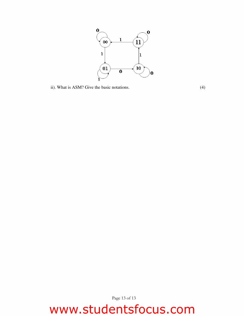
10. i). For the state diagram shown in below figure, design a synchronous sequential
circuit using JK flip flops. (12)
www.studentsfocus.com
Page 13 of 13
ii). What is ASM? Give the basic notations. (4)
www.studentsfocus.com
![Power Efficient CMOS Full Adders with Reduced Transistor Count · The TGA full adder [5] using 20 transistors is based on CMOS transmission gates and CMOS inverters. It ... In TFA](https://static.fdocument.org/doc/165x107/5c01a10709d3f20f068d0c17/power-efficient-cmos-full-adders-with-reduced-transistor-count-the-tga-full.jpg)