SN54HCT14, SN74HCT14 HEX SCHMITT-TRIGGER INVERTERS … · SN54HCT14, SN74HCT14 HEX SCHMITT-TRIGGER...
21
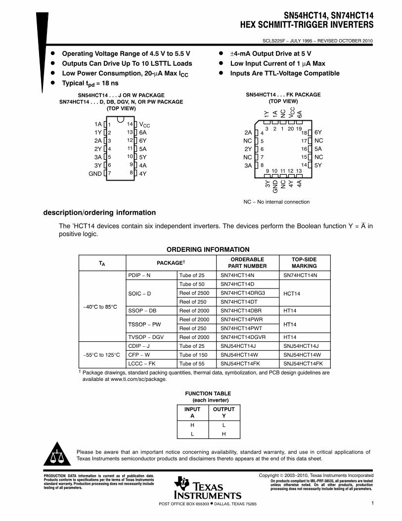
SN54HCT14, SN74HCT14 HEX SCHMITT-TRIGGER INVERTERS SCLS225F − JULY 1995 − REVISED OCTOBER 2010 1 POST OFFICE BOX 655303 • DALLAS, TEXAS 75265 D Operating Voltage Range of 4.5 V to 5.5 V D Outputs Can Drive Up To 10 LSTTL Loads D Low Power Consumption, 20-μA Max I CC D Typical t pd = 18 ns D ±4-mA Output Drive at 5 V D Low Input Current of 1 μA Max D Inputs Are TTL-Voltage Compatible 1 2 3 4 5 6 7 14 13 12 11 10 9 8 1A 1Y 2A 2Y 3A 3Y GND V CC 6A 6Y 5A 5Y 4A 4Y SN54HCT14 . . . J OR W PACKAGE SN74HCT14 . . . D, DB, DGV, N, OR PW PACKAGE (TOP VIEW) 3 2 1 20 19 9 10 11 12 13 4 5 6 7 8 18 17 16 15 14 6Y NC 5A NC 5Y 2A NC 2Y NC 3A 1Y 1A NC 4Y 4A V 6A 3Y GND NC SN54HCT14 . . . FK PACKAGE (TOP VIEW) CC NC − No internal connection description/ordering information The ’HCT14 devices contain six independent inverters. The devices perform the Boolean function Y = A in positive logic. ORDERING INFORMATION T A PACKAGE † ORDERABLE PART NUMBER TOP-SIDE MARKING PDIP − N Tube of 25 SN74HCT14N SN74HCT14N Tube of 50 SN74HCT14D SOIC − D Reel of 2500 SN74HCT14DRG3 HCT14 40°C to 85°C SOIC D Reel of 250 SN74HCT14DT HCT14 −40°C to 85°C SSOP − DB Reel of 2000 SN74HCT14DBR HT14 TSSOP PW Reel of 2000 SN74HCT14PWR HT14 TSSOP − PW Reel of 250 SN74HCT14PWT HT14 TVSOP − DGV Reel of 2000 SN74HCT14DGVR HT14 CDIP − J Tube of 25 SNJ54HCT14J SNJ54HCT14J −55°C to 125°C CFP − W Tube of 150 SNJ54HCT14W SNJ54HCT14W LCCC − FK Tube of 55 SNJ54HCT14FK SNJ54HCT14FK † Package drawings, standard packing quantities, thermal data, symbolization, and PCB design guidelines are available at www.ti.com/sc/package. FUNCTION TABLE (each inverter) INPUT A OUTPUT Y H L L H Copyright © 2003−2010, Texas Instruments Incorporated Please be aware that an important notice concerning availability, standard warranty, and use in critical applications of Texas Instruments semiconductor products and disclaimers thereto appears at the end of this data sheet. PRODUCTION DATA information is current as of publication date. Products conform to specifications per the terms of Texas Instruments standard warranty. Production processing does not necessarily include testing of all parameters. On products compliant to MIL-PRF-38535, all parameters are tested unless otherwise noted. On all other products, production processing does not necessarily include testing of all parameters.
Transcript of SN54HCT14, SN74HCT14 HEX SCHMITT-TRIGGER INVERTERS … · SN54HCT14, SN74HCT14 HEX SCHMITT-TRIGGER...
SN54HCT14, SN74HCT14HEX SCHMITT-TRIGGER INVERTERS
SCLS225F − JULY 1995 − REVISED OCTOBER 2010
1POST OFFICE BOX 655303 • DALLAS, TEXAS 75265
� Operating Voltage Range of 4.5 V to 5.5 V
� Outputs Can Drive Up To 10 LSTTL Loads
� Low Power Consumption, 20-μA Max ICC
� Typical tpd = 18 ns
� ±4-mA Output Drive at 5 V
� Low Input Current of 1 μA Max
� Inputs Are TTL-Voltage Compatible
1
2
3
4
5
6
7
14
13
12
11
10
9
8
1A1Y2A2Y3A3Y
GND
VCC
6A6Y5A5Y4A4Y
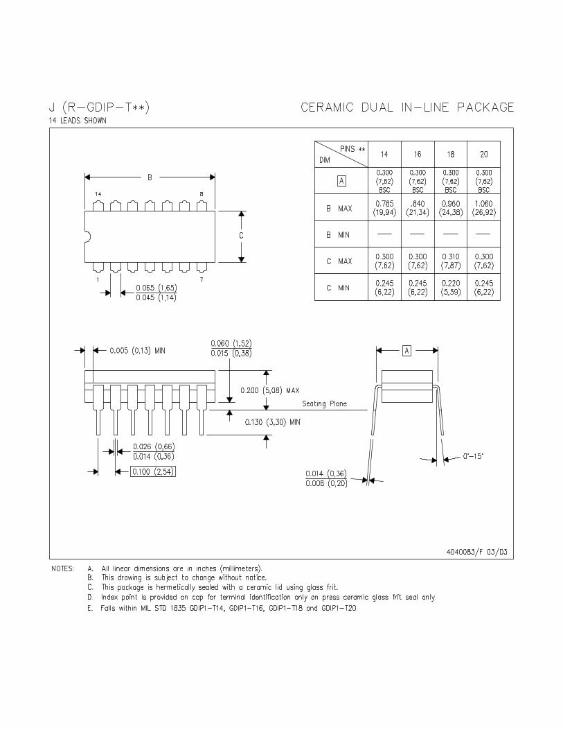
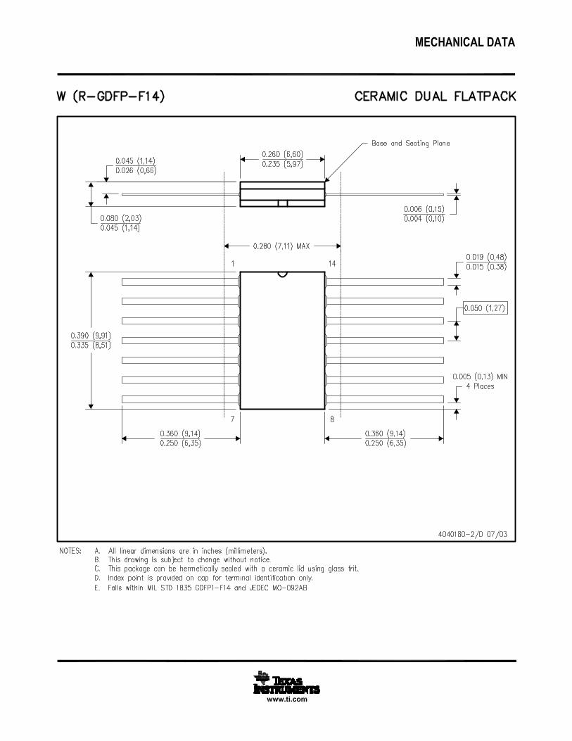
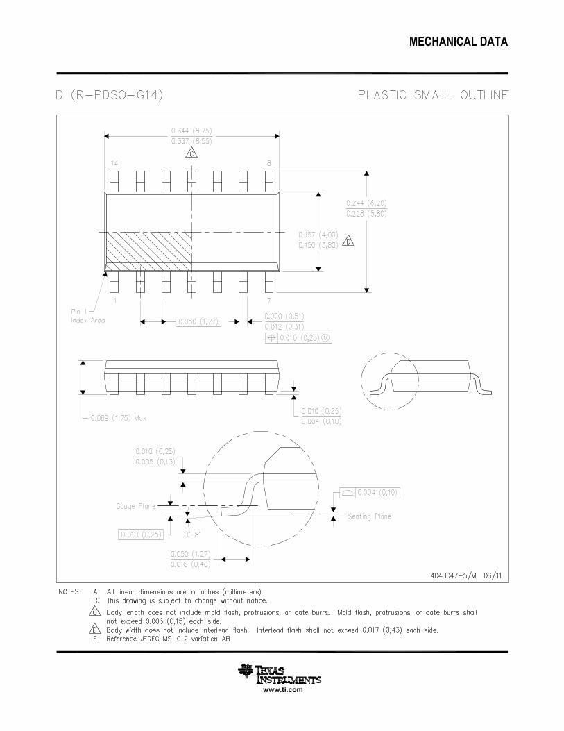
SN54HCT14 . . . J OR W PACKAGESN74HCT14 . . . D, DB, DGV, N, OR PW PACKAGE
(TOP VIEW)
3 2 1 20 19
9 10 11 12 13
4
5
6
7
8
18
17
16
15
14
6YNC5ANC5Y
2ANC2YNC3A
1Y 1A NC
4Y 4AV 6A
3YG
ND
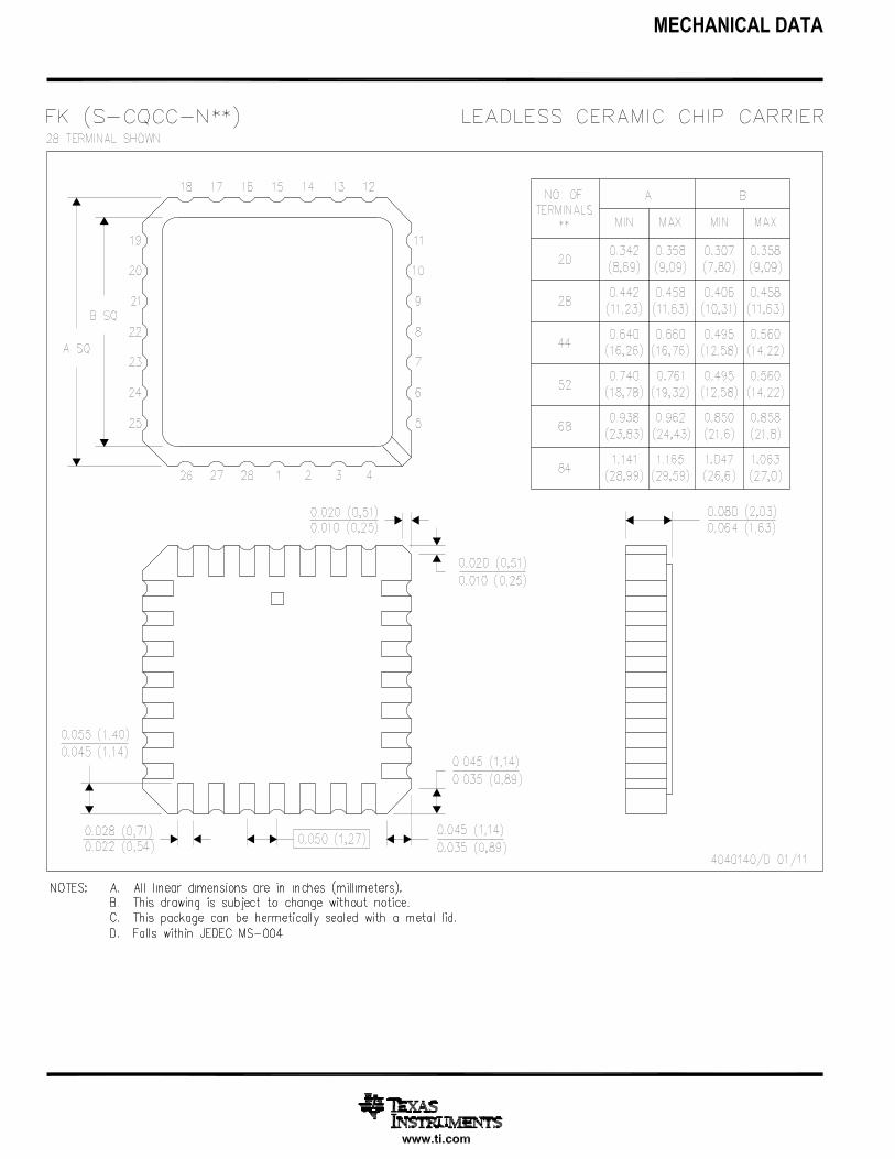
NC
SN54HCT14 . . . FK PACKAGE(TOP VIEW)
CC
NC − No internal connection
description/ordering information
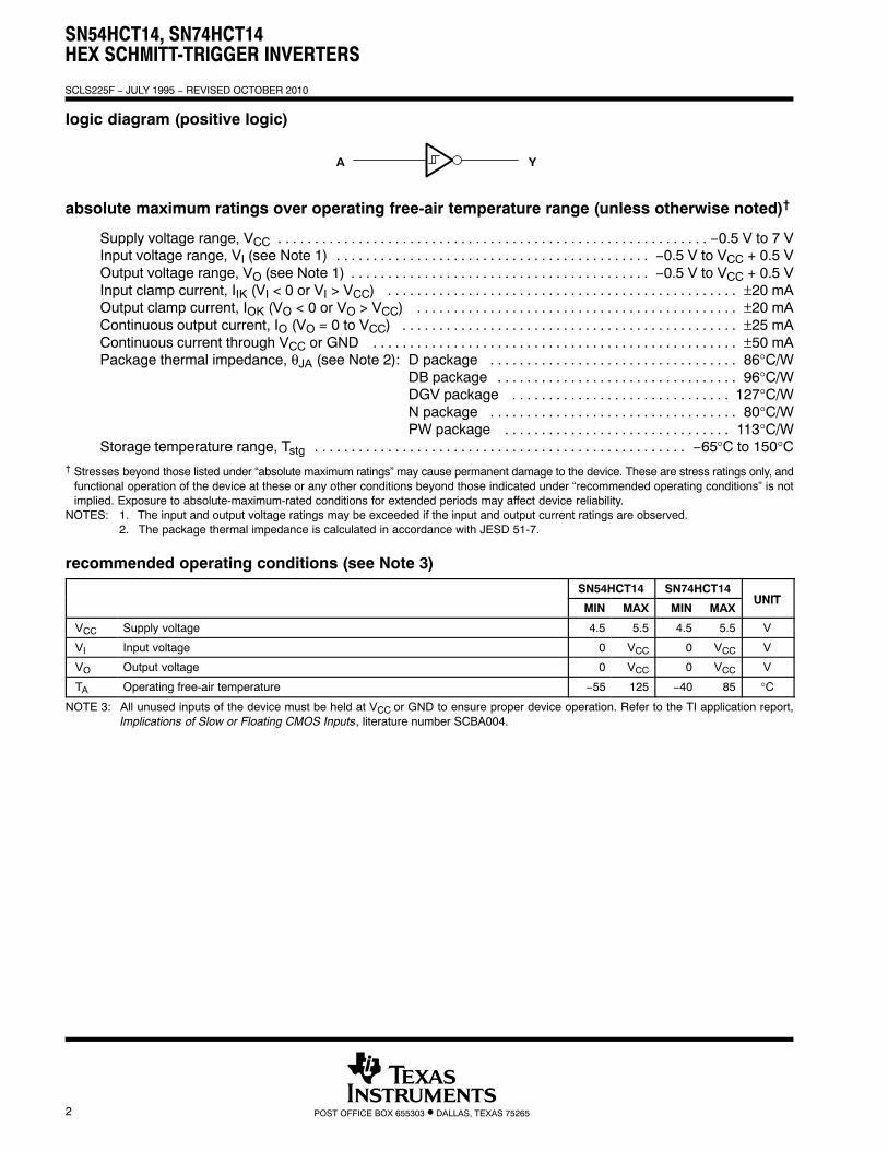
The ’HCT14 devices contain six independent inverters. The devices perform the Boolean function Y = A inpositive logic.
ORDERING INFORMATION
TA PACKAGE† ORDERABLEPART NUMBER
TOP-SIDEMARKING
PDIP − N Tube of 25 SN74HCT14N SN74HCT14N
Tube of 50 SN74HCT14D
SOIC − D Reel of 2500 SN74HCT14DRG3 HCT14
40°C to 85°C
SOIC D
Reel of 250 SN74HCT14DT
HCT14
−40°C to 85°CSSOP − DB Reel of 2000 SN74HCT14DBR HT14
TSSOP PWReel of 2000 SN74HCT14PWR
HT14TSSOP − PWReel of 250 SN74HCT14PWT
HT14
TVSOP − DGV Reel of 2000 SN74HCT14DGVR HT14
CDIP − J Tube of 25 SNJ54HCT14J SNJ54HCT14J
−55°C to 125°C CFP − W Tube of 150 SNJ54HCT14W SNJ54HCT14W
LCCC − FK Tube of 55 SNJ54HCT14FK SNJ54HCT14FK† Package drawings, standard packing quantities, thermal data, symbolization, and PCB design guidelines are
available at www.ti.com/sc/package.
FUNCTION TABLE(each inverter)
INPUTA
OUTPUTY
H L
L H
Copyright © 2003−2010, Texas Instruments Incorporated
Please be aware that an important notice concerning availability, standard warranty, and use in critical applications ofTexas Instruments semiconductor products and disclaimers thereto appears at the end of this data sheet.
PRODUCTION DATA information is current as of publication date.Products conform to specifications per the terms of Texas Instrumentsstandard warranty. Production processing does not necessarily includetesting of all parameters.
On products compliant to MIL-PRF-38535, all parameters are testedunless otherwise noted. On all other products, productionprocessing does not necessarily include testing of all parameters.
SN54HCT14, SN74HCT14HEX SCHMITT-TRIGGER INVERTERS
SCLS225F − JULY 1995 − REVISED OCTOBER 2010
2 POST OFFICE BOX 655303 • DALLAS, TEXAS 75265
logic diagram (positive logic)
A Y
absolute maximum ratings over operating free-air temperature range (unless otherwise noted)†
Supply voltage range, VCC −0.5 V to 7 V. . . . . . . . . . . . . . . . . . . . . . . . . . . . . . . . . . . . . . . . . . . . . . . . . . . . . . . . . . . Input voltage range, VI (see Note 1) −0.5 V to VCC + 0.5 V. . . . . . . . . . . . . . . . . . . . . . . . . . . . . . . . . . . . . . . . . . . Output voltage range, VO (see Note 1) −0.5 V to VCC + 0.5 V. . . . . . . . . . . . . . . . . . . . . . . . . . . . . . . . . . . . . . . . . Input clamp current, IIK (VI < 0 or VI > VCC) ±20 mA. . . . . . . . . . . . . . . . . . . . . . . . . . . . . . . . . . . . . . . . . . . . . . . . Output clamp current, IOK (VO < 0 or VO > VCC) ±20 mA. . . . . . . . . . . . . . . . . . . . . . . . . . . . . . . . . . . . . . . . . . . . Continuous output current, IO (VO = 0 to VCC) ±25 mA. . . . . . . . . . . . . . . . . . . . . . . . . . . . . . . . . . . . . . . . . . . . . . Continuous current through VCC or GND ±50 mA. . . . . . . . . . . . . . . . . . . . . . . . . . . . . . . . . . . . . . . . . . . . . . . . . . Package thermal impedance, θJA (see Note 2): D package 86°C/W. . . . . . . . . . . . . . . . . . . . . . . . . . . . . . . . . .
DB package 96°C/W. . . . . . . . . . . . . . . . . . . . . . . . . . . . . . . . . DGV package 127°C/W. . . . . . . . . . . . . . . . . . . . . . . . . . . . . . N package 80°C/W. . . . . . . . . . . . . . . . . . . . . . . . . . . . . . . . . . PW package 113°C/W. . . . . . . . . . . . . . . . . . . . . . . . . . . . . . .
Storage temperature range, Tstg −65°C to 150°C. . . . . . . . . . . . . . . . . . . . . . . . . . . . . . . . . . . . . . . . . . . . . . . . . . . † Stresses beyond those listed under “absolute maximum ratings” may cause permanent damage to the device. These are stress ratings only, and
functional operation of the device at these or any other conditions beyond those indicated under “recommended operating conditions” is notimplied. Exposure to absolute-maximum-rated conditions for extended periods may affect device reliability.
NOTES: 1. The input and output voltage ratings may be exceeded if the input and output current ratings are observed.2. The package thermal impedance is calculated in accordance with JESD 51-7.
recommended operating conditions (see Note 3)
SN54HCT14 SN74HCT14UNIT
MIN MAX MIN MAXUNIT
VCC Supply voltage 4.5 5.5 4.5 5.5 V
VI Input voltage 0 VCC 0 VCC V
VO Output voltage 0 VCC 0 VCC V
TA Operating free-air temperature −55 125 −40 85 °C
NOTE 3: All unused inputs of the device must be held at VCC or GND to ensure proper device operation. Refer to the TI application report,Implications of Slow or Floating CMOS Inputs, literature number SCBA004.
SN54HCT14, SN74HCT14HEX SCHMITT-TRIGGER INVERTERS
SCLS225F − JULY 1995 − REVISED OCTOBER 2010
3POST OFFICE BOX 655303 • DALLAS, TEXAS 75265
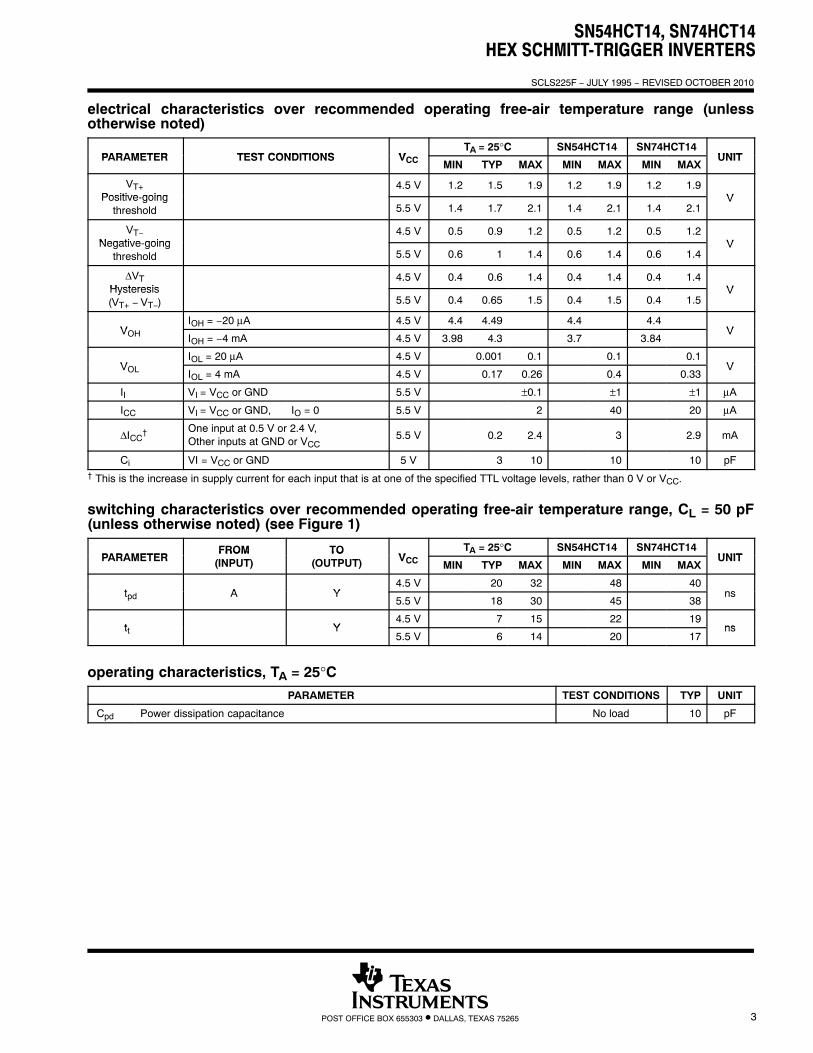
electrical characteristics over recommended operating free-air temperature range (unlessotherwise noted)
PARAMETER TEST CONDITIONS VTA = 25°C SN54HCT14 SN74HCT14
UNITPARAMETER TEST CONDITIONS VCC MIN TYP MAX MIN MAX MIN MAXUNIT
VT+Positive going
4.5 V 1.2 1.5 1.9 1.2 1.9 1.2 1.9VPositive-going
threshold 5.5 V 1.4 1.7 2.1 1.4 2.1 1.4 2.1V
VT−Negative going
4.5 V 0.5 0.9 1.2 0.5 1.2 0.5 1.2VNegative-going
threshold 5.5 V 0.6 1 1.4 0.6 1.4 0.6 1.4V
ΔVTHysteresis
4.5 V 0.4 0.6 1.4 0.4 1.4 0.4 1.4VHysteresis
(VT+ − VT−) 5.5 V 0.4 0.65 1.5 0.4 1.5 0.4 1.5V
VIOH = −20 μA 4.5 V 4.4 4.49 4.4 4.4
VVOH IOH = −4 mA 4.5 V 3.98 4.3 3.7 3.84V
VIOL = 20 μA 4.5 V 0.001 0.1 0.1 0.1
VVOL IOL = 4 mA 4.5 V 0.17 0.26 0.4 0.33V
II VI = VCC or GND 5.5 V ±0.1 ±1 ±1 μA
ICC VI = VCC or GND, IO = 0 5.5 V 2 40 20 μA
ΔICC† One input at 0.5 V or 2.4 V,
Other inputs at GND or VCC5.5 V 0.2 2.4 3 2.9 mA
Ci VI = VCC or GND 5 V 3 10 10 10 pF† This is the increase in supply current for each input that is at one of the specified TTL voltage levels, rather than 0 V or VCC.
switching characteristics over recommended operating free-air temperature range, CL = 50 pF(unless otherwise noted) (see Figure 1)
PARAMETERFROM TO
VTA = 25°C SN54HCT14 SN74HCT14
UNITPARAMETERFROM
(INPUT)TO
(OUTPUT) VCC MIN TYP MAX MIN MAX MIN MAXUNIT
t A Y4.5 V 20 32 48 40
nstpd A Y5.5 V 18 30 45 38
ns
t Y4.5 V 7 15 22 19
nstt Y5.5 V 6 14 20 17
ns
operating characteristics, TA = 25°CPARAMETER TEST CONDITIONS TYP UNIT
Cpd Power dissipation capacitance No load 10 pF
SN54HCT14, SN74HCT14HEX SCHMITT-TRIGGER INVERTERS
SCLS225F − JULY 1995 − REVISED OCTOBER 2010
4 POST OFFICE BOX 655303 • DALLAS, TEXAS 75265
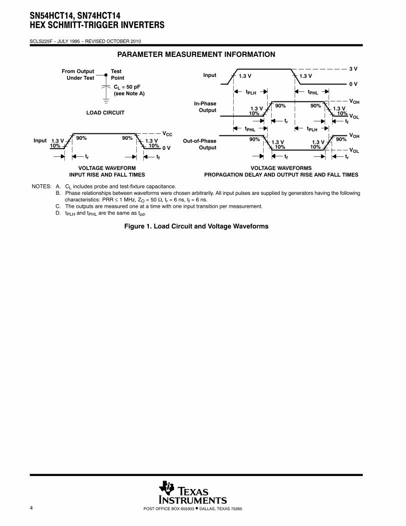
PARAMETER MEASUREMENT INFORMATION
VOLTAGE WAVEFORMINPUT RISE AND FALL TIMES
VOLTAGE WAVEFORMSPROPAGATION DELAY AND OUTPUT RISE AND FALL TIMES
1.3 V
1.3 V1.3 V10%10%
90% 90%
3 V
VOH
VOL
0 V
tr tf
Input
In-PhaseOutput
1.3 V
tPLH tPHL
1.3 V 1.3 V10% 10%
90%90%VOH
VOLtrtf
tPHL tPLH
Out-of-PhaseOutput
TestPoint
From OutputUnder Test
LOAD CIRCUIT
NOTES: A. CL includes probe and test-fixture capacitance.B. Phase relationships between waveforms were chosen arbitrarily. All input pulses are supplied by generators having the following
characteristics: PRR ≤ 1 MHz, ZO = 50 Ω, tr = 6 ns, tf = 6 ns.C. The outputs are measured one at a time with one input transition per measurement.D. tPLH and tPHL are the same as tpd.
CL = 50 pF(see Note A)
1.3 V1.3 V10%10%
90% 90%VCC
0 V
tr tf
Input
Figure 1. Load Circuit and Voltage Waveforms
SN54HCT14, SN74HCT14HEX SCHMITT-TRIGGER INVERTERS
SCLS225F − JULY 1995 − REVISED OCTOBER 2010
5POST OFFICE BOX 655303 • DALLAS, TEXAS 75265
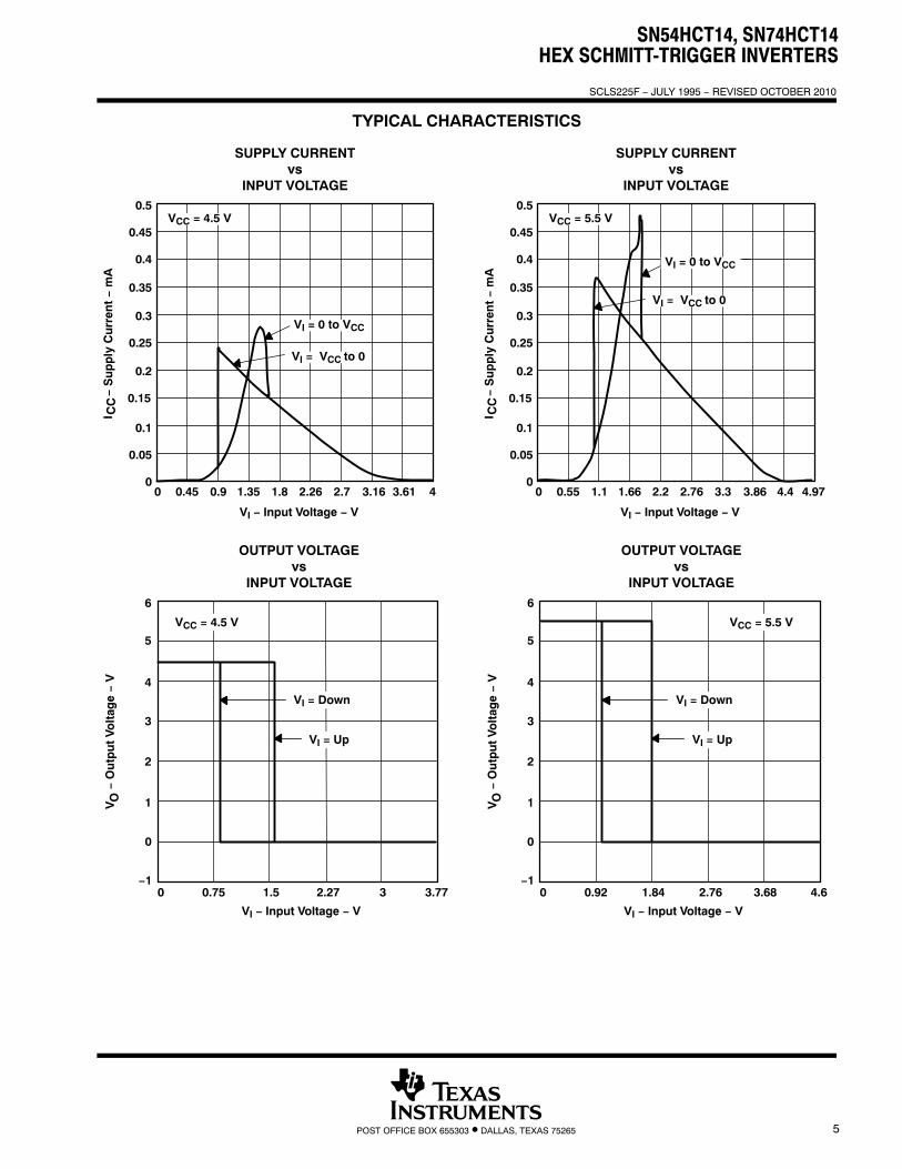
TYPICAL CHARACTERISTICS
0.25
0.2
0.1
0.05
0
0.45
0.15
0 0.45 0.9 1.35 1.8 2.26 2.7
− S
up
ply
Cu
rren
t −
mA
0.35
0.3
0.4
SUPPLY CURRENTvs
INPUT VOLTAGE0.5
3.16 3.61 4
VI − Input Voltage − V
ÁÁÁÁ
I CC
VI = 0 to VCC
VI = VCC to 0
VCC = 4.5 V
0.25
0.2
0.1
0.05
0
0.45
0.15
0 0.55 1.1 1.66 2.2 2.76 3.3−
Su
pp
ly C
urr
ent −
mA
0.35
0.3
0.4
SUPPLY CURRENTvs
INPUT VOLTAGE0.5
3.86 4.4 4.97
VI − Input Voltage − V
ÁÁÁÁ
I CC
VI = 0 to VCC
VI = VCC to 0
VCC = 5.5 V
0 0.75 1.5 2.27
− O
utp
ut
Volt
age −
V
OUTPUT VOLTAGEvs
INPUT VOLTAGE
3 3.77
6
5
4
3
2
1
0
−1
VO
VI − Input Voltage − V
VI = Down
VI = Up
VCC = 4.5 V
0 0.92 1.84 2.76
− O
utp
ut
Volt
age −
V
OUTPUT VOLTAGEvs
INPUT VOLTAGE
3.68 4.6
6
5
4
3
2
1
0
−1
VO
VI − Input Voltage − V
VI = Down
VI = Up
VCC = 5.5 V
PACKAGE OPTION ADDENDUM
www.ti.com 5-Sep-2011
Addendum-Page 1
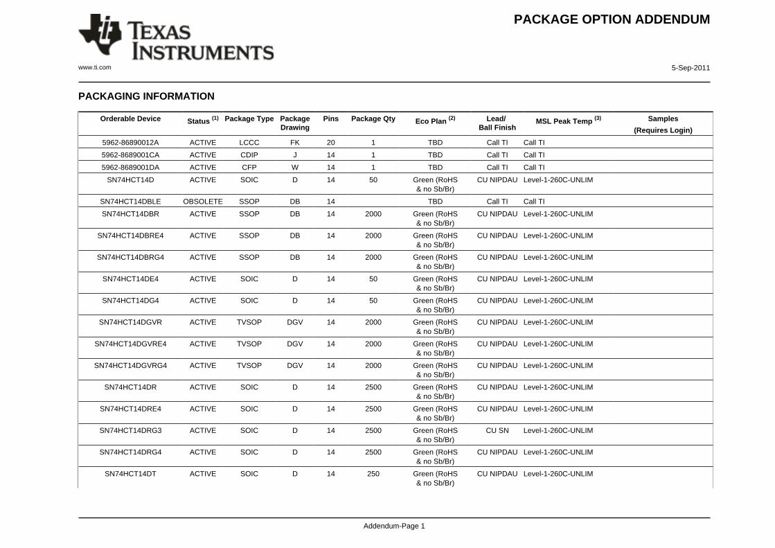
PACKAGING INFORMATION
Orderable Device Status (1) Package Type PackageDrawing
Pins Package Qty Eco Plan (2) Lead/Ball Finish
MSL Peak Temp (3) Samples
(Requires Login)
5962-86890012A ACTIVE LCCC FK 20 1 TBD Call TI Call TI
5962-8689001CA ACTIVE CDIP J 14 1 TBD Call TI Call TI
5962-8689001DA ACTIVE CFP W 14 1 TBD Call TI Call TI
SN74HCT14D ACTIVE SOIC D 14 50 Green (RoHS& no Sb/Br)
CU NIPDAU Level-1-260C-UNLIM
SN74HCT14DBLE OBSOLETE SSOP DB 14 TBD Call TI Call TI
SN74HCT14DBR ACTIVE SSOP DB 14 2000 Green (RoHS& no Sb/Br)
CU NIPDAU Level-1-260C-UNLIM
SN74HCT14DBRE4 ACTIVE SSOP DB 14 2000 Green (RoHS& no Sb/Br)
CU NIPDAU Level-1-260C-UNLIM
SN74HCT14DBRG4 ACTIVE SSOP DB 14 2000 Green (RoHS& no Sb/Br)
CU NIPDAU Level-1-260C-UNLIM
SN74HCT14DE4 ACTIVE SOIC D 14 50 Green (RoHS& no Sb/Br)
CU NIPDAU Level-1-260C-UNLIM
SN74HCT14DG4 ACTIVE SOIC D 14 50 Green (RoHS& no Sb/Br)
CU NIPDAU Level-1-260C-UNLIM
SN74HCT14DGVR ACTIVE TVSOP DGV 14 2000 Green (RoHS& no Sb/Br)
CU NIPDAU Level-1-260C-UNLIM
SN74HCT14DGVRE4 ACTIVE TVSOP DGV 14 2000 Green (RoHS& no Sb/Br)
CU NIPDAU Level-1-260C-UNLIM
SN74HCT14DGVRG4 ACTIVE TVSOP DGV 14 2000 Green (RoHS& no Sb/Br)
CU NIPDAU Level-1-260C-UNLIM
SN74HCT14DR ACTIVE SOIC D 14 2500 Green (RoHS& no Sb/Br)
CU NIPDAU Level-1-260C-UNLIM
SN74HCT14DRE4 ACTIVE SOIC D 14 2500 Green (RoHS& no Sb/Br)
CU NIPDAU Level-1-260C-UNLIM
SN74HCT14DRG3 ACTIVE SOIC D 14 2500 Green (RoHS& no Sb/Br)
CU SN Level-1-260C-UNLIM
SN74HCT14DRG4 ACTIVE SOIC D 14 2500 Green (RoHS& no Sb/Br)
CU NIPDAU Level-1-260C-UNLIM
SN74HCT14DT ACTIVE SOIC D 14 250 Green (RoHS& no Sb/Br)
CU NIPDAU Level-1-260C-UNLIM
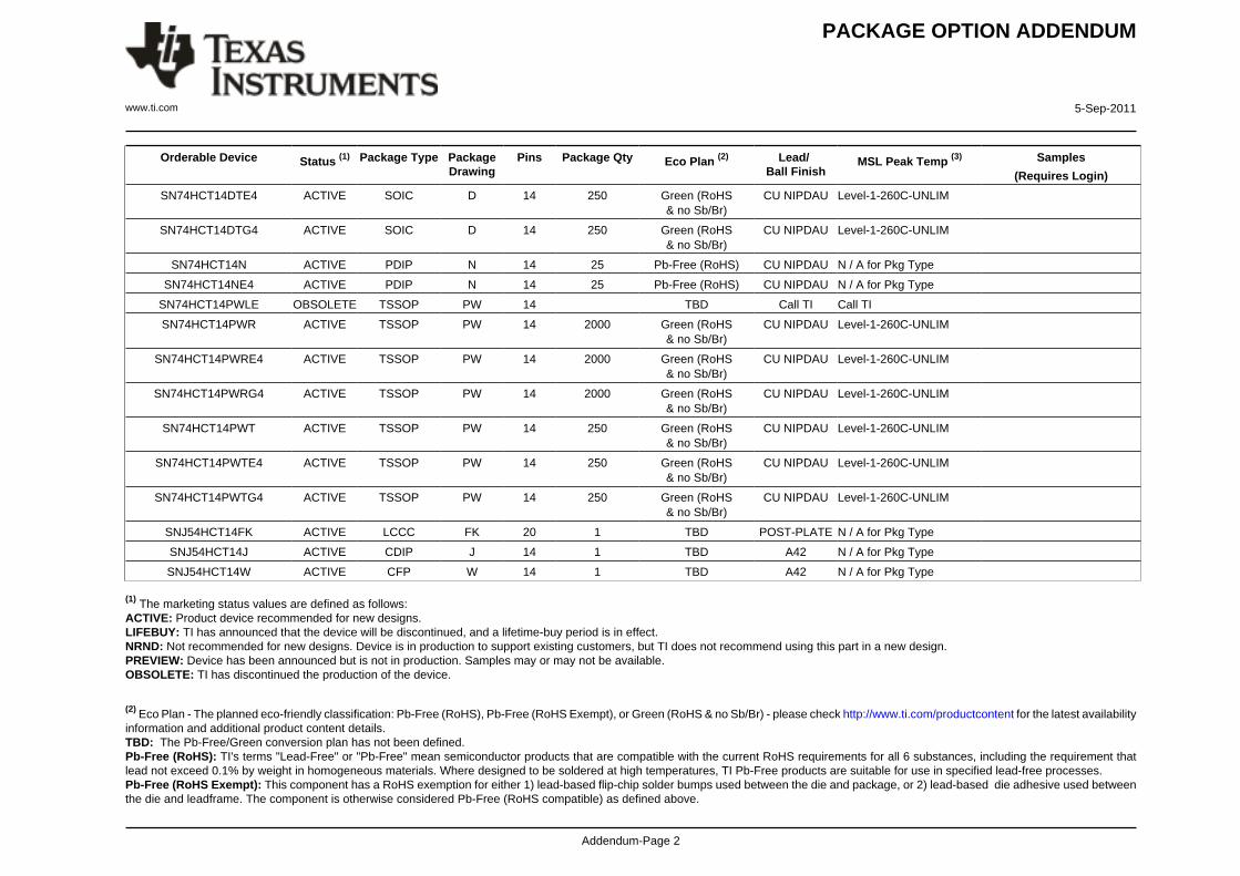
PACKAGE OPTION ADDENDUM
www.ti.com 5-Sep-2011
Addendum-Page 2
Orderable Device Status (1) Package Type PackageDrawing
Pins Package Qty Eco Plan (2) Lead/Ball Finish
MSL Peak Temp (3) Samples
(Requires Login)
SN74HCT14DTE4 ACTIVE SOIC D 14 250 Green (RoHS& no Sb/Br)
CU NIPDAU Level-1-260C-UNLIM
SN74HCT14DTG4 ACTIVE SOIC D 14 250 Green (RoHS& no Sb/Br)
CU NIPDAU Level-1-260C-UNLIM
SN74HCT14N ACTIVE PDIP N 14 25 Pb-Free (RoHS) CU NIPDAU N / A for Pkg Type
SN74HCT14NE4 ACTIVE PDIP N 14 25 Pb-Free (RoHS) CU NIPDAU N / A for Pkg Type
SN74HCT14PWLE OBSOLETE TSSOP PW 14 TBD Call TI Call TI
SN74HCT14PWR ACTIVE TSSOP PW 14 2000 Green (RoHS& no Sb/Br)
CU NIPDAU Level-1-260C-UNLIM
SN74HCT14PWRE4 ACTIVE TSSOP PW 14 2000 Green (RoHS& no Sb/Br)
CU NIPDAU Level-1-260C-UNLIM
SN74HCT14PWRG4 ACTIVE TSSOP PW 14 2000 Green (RoHS& no Sb/Br)
CU NIPDAU Level-1-260C-UNLIM
SN74HCT14PWT ACTIVE TSSOP PW 14 250 Green (RoHS& no Sb/Br)
CU NIPDAU Level-1-260C-UNLIM
SN74HCT14PWTE4 ACTIVE TSSOP PW 14 250 Green (RoHS& no Sb/Br)
CU NIPDAU Level-1-260C-UNLIM
SN74HCT14PWTG4 ACTIVE TSSOP PW 14 250 Green (RoHS& no Sb/Br)
CU NIPDAU Level-1-260C-UNLIM
SNJ54HCT14FK ACTIVE LCCC FK 20 1 TBD POST-PLATE N / A for Pkg Type
SNJ54HCT14J ACTIVE CDIP J 14 1 TBD A42 N / A for Pkg Type
SNJ54HCT14W ACTIVE CFP W 14 1 TBD A42 N / A for Pkg Type (1) The marketing status values are defined as follows:ACTIVE: Product device recommended for new designs.LIFEBUY: TI has announced that the device will be discontinued, and a lifetime-buy period is in effect.NRND: Not recommended for new designs. Device is in production to support existing customers, but TI does not recommend using this part in a new design.PREVIEW: Device has been announced but is not in production. Samples may or may not be available.OBSOLETE: TI has discontinued the production of the device.
(2) Eco Plan - The planned eco-friendly classification: Pb-Free (RoHS), Pb-Free (RoHS Exempt), or Green (RoHS & no Sb/Br) - please check http://www.ti.com/productcontent for the latest availabilityinformation and additional product content details.TBD: The Pb-Free/Green conversion plan has not been defined.Pb-Free (RoHS): TI's terms "Lead-Free" or "Pb-Free" mean semiconductor products that are compatible with the current RoHS requirements for all 6 substances, including the requirement thatlead not exceed 0.1% by weight in homogeneous materials. Where designed to be soldered at high temperatures, TI Pb-Free products are suitable for use in specified lead-free processes.Pb-Free (RoHS Exempt): This component has a RoHS exemption for either 1) lead-based flip-chip solder bumps used between the die and package, or 2) lead-based die adhesive used betweenthe die and leadframe. The component is otherwise considered Pb-Free (RoHS compatible) as defined above.
PACKAGE OPTION ADDENDUM
www.ti.com 5-Sep-2011
Addendum-Page 3
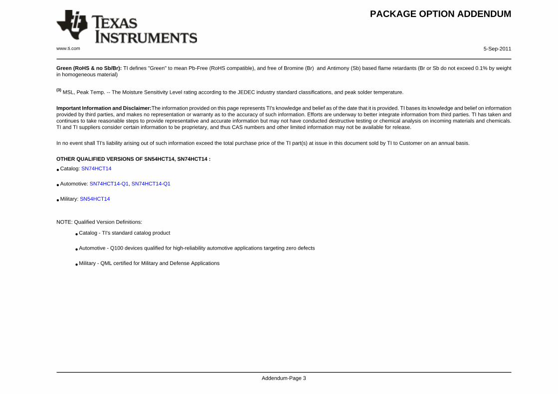
Green (RoHS & no Sb/Br): TI defines "Green" to mean Pb-Free (RoHS compatible), and free of Bromine (Br) and Antimony (Sb) based flame retardants (Br or Sb do not exceed 0.1% by weightin homogeneous material)
(3) MSL, Peak Temp. -- The Moisture Sensitivity Level rating according to the JEDEC industry standard classifications, and peak solder temperature.
Important Information and Disclaimer:The information provided on this page represents TI's knowledge and belief as of the date that it is provided. TI bases its knowledge and belief on informationprovided by third parties, and makes no representation or warranty as to the accuracy of such information. Efforts are underway to better integrate information from third parties. TI has taken andcontinues to take reasonable steps to provide representative and accurate information but may not have conducted destructive testing or chemical analysis on incoming materials and chemicals.TI and TI suppliers consider certain information to be proprietary, and thus CAS numbers and other limited information may not be available for release.
In no event shall TI's liability arising out of such information exceed the total purchase price of the TI part(s) at issue in this document sold by TI to Customer on an annual basis.
OTHER QUALIFIED VERSIONS OF SN54HCT14, SN74HCT14 :
• Catalog: SN74HCT14
• Automotive: SN74HCT14-Q1, SN74HCT14-Q1
• Military: SN54HCT14
NOTE: Qualified Version Definitions:
• Catalog - TI's standard catalog product
• Automotive - Q100 devices qualified for high-reliability automotive applications targeting zero defects
• Military - QML certified for Military and Defense Applications
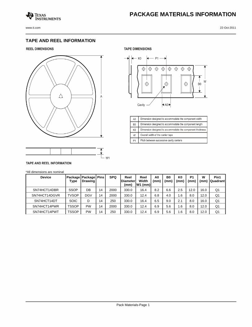
TAPE AND REEL INFORMATION
*All dimensions are nominal
Device PackageType
PackageDrawing
Pins SPQ ReelDiameter
(mm)
ReelWidth
W1 (mm)
A0(mm)
B0(mm)
K0(mm)
P1(mm)
W(mm)
Pin1Quadrant
SN74HCT14DBR SSOP DB 14 2000 330.0 16.4 8.2 6.6 2.5 12.0 16.0 Q1
SN74HCT14DGVR TVSOP DGV 14 2000 330.0 12.4 6.8 4.0 1.6 8.0 12.0 Q1
SN74HCT14DT SOIC D 14 250 330.0 16.4 6.5 9.0 2.1 8.0 16.0 Q1
SN74HCT14PWR TSSOP PW 14 2000 330.0 12.4 6.9 5.6 1.6 8.0 12.0 Q1
SN74HCT14PWT TSSOP PW 14 250 330.0 12.4 6.9 5.6 1.6 8.0 12.0 Q1
PACKAGE MATERIALS INFORMATION
www.ti.com 22-Oct-2011
Pack Materials-Page 1
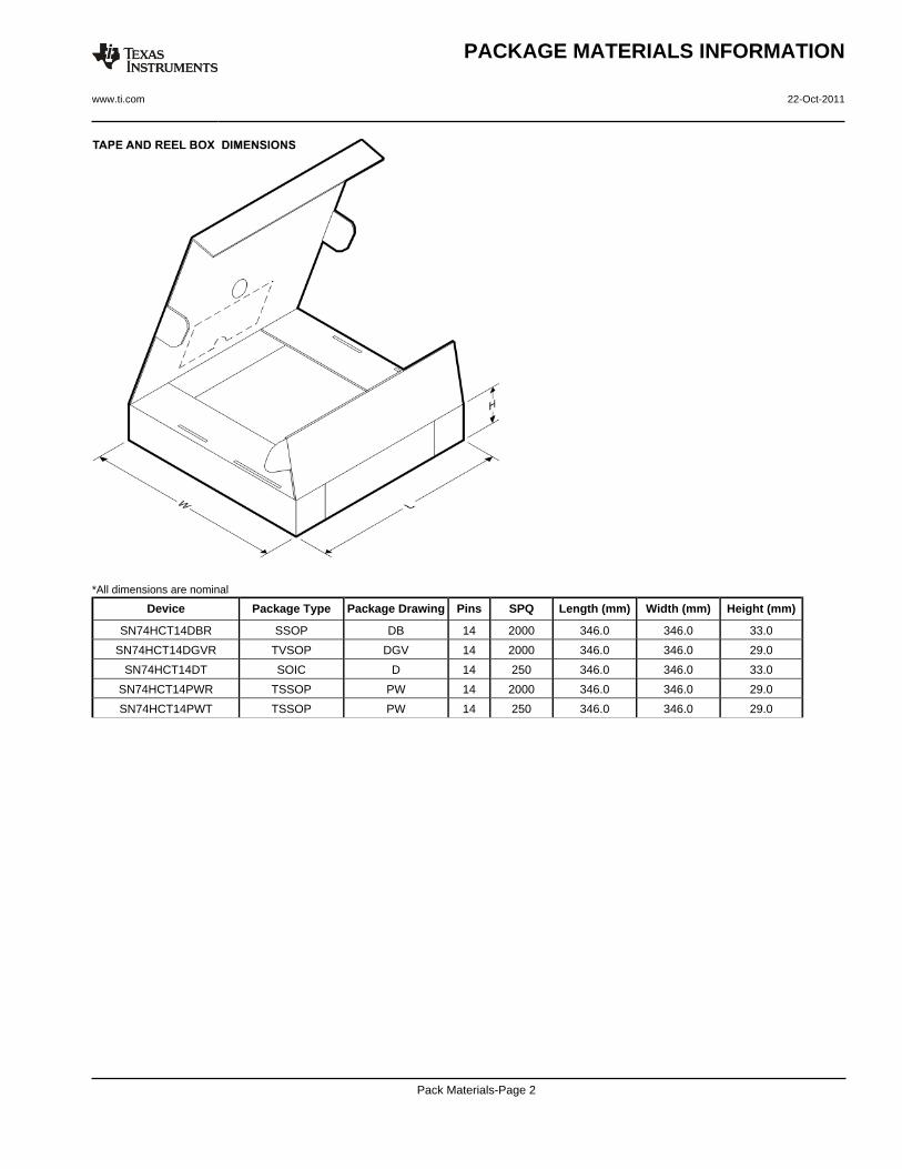
*All dimensions are nominal
Device Package Type Package Drawing Pins SPQ Length (mm) Width (mm) Height (mm)
SN74HCT14DBR SSOP DB 14 2000 346.0 346.0 33.0
SN74HCT14DGVR TVSOP DGV 14 2000 346.0 346.0 29.0
SN74HCT14DT SOIC D 14 250 346.0 346.0 33.0
SN74HCT14PWR TSSOP PW 14 2000 346.0 346.0 29.0
SN74HCT14PWT TSSOP PW 14 250 346.0 346.0 29.0
PACKAGE MATERIALS INFORMATION
www.ti.com 22-Oct-2011
Pack Materials-Page 2
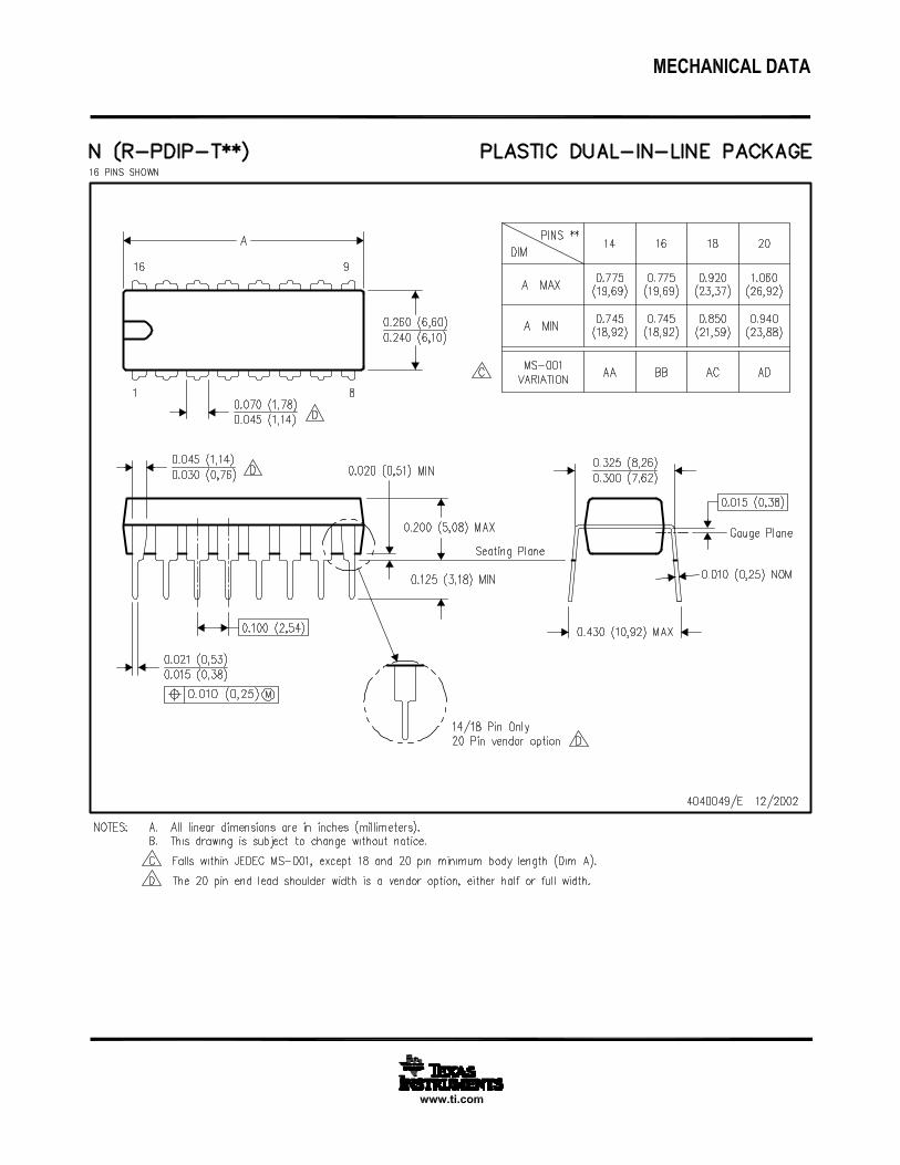
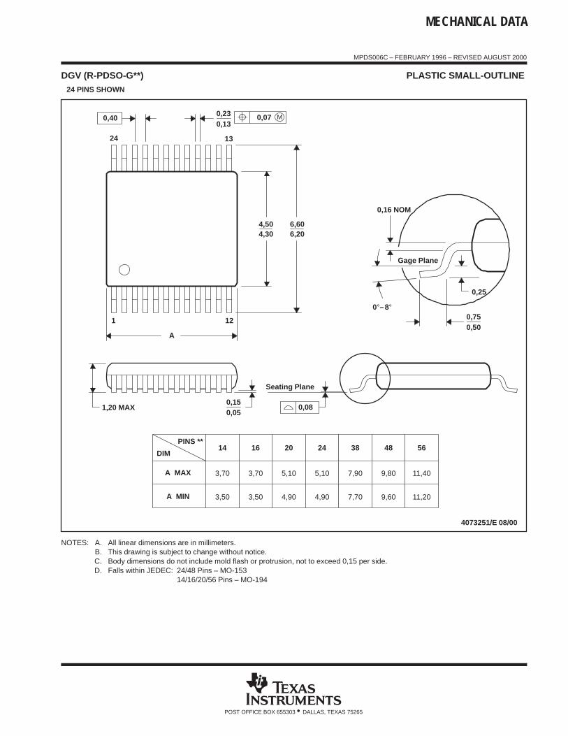
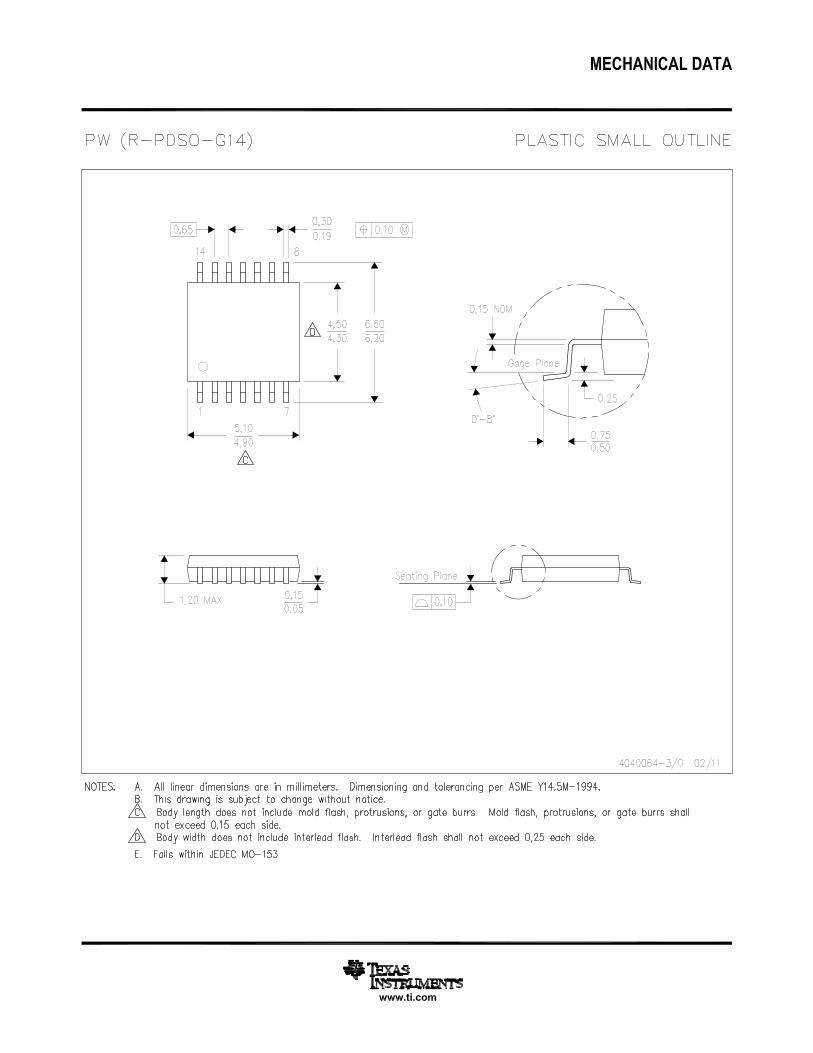
MECHANICAL DATA
MPDS006C – FEBRUARY 1996 – REVISED AUGUST 2000
POST OFFICE BOX 655303 • DALLAS, TEXAS 75265
DGV (R-PDSO-G**) PLASTIC SMALL-OUTLINE 24 PINS SHOWN
14
3,70
3,50 4,90
5,10
20DIM
PINS **
4073251/E 08/00
1,20 MAX
Seating Plane
0,050,15
0,25
0,500,75
0,230,13
1 12
24 13
4,304,50
0,16 NOM
Gage Plane
A
7,90
7,70
382416
4,90
5,103,70
3,50
A MAX
A MIN
6,606,20
11,20
11,40
56
9,60
9,80
48
0,08
M0,070,40
0°–�8°
NOTES: A. All linear dimensions are in millimeters.B. This drawing is subject to change without notice.C. Body dimensions do not include mold flash or protrusion, not to exceed 0,15 per side.D. Falls within JEDEC: 24/48 Pins – MO-153
14/16/20/56 Pins – MO-194
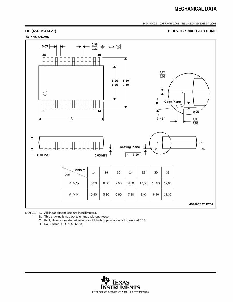
MECHANICAL DATA
MSSO002E – JANUARY 1995 – REVISED DECEMBER 2001
POST OFFICE BOX 655303 • DALLAS, TEXAS 75265
DB (R-PDSO-G**) PLASTIC SMALL-OUTLINE
4040065 /E 12/01
28 PINS SHOWN
Gage Plane
8,207,40
0,550,95
0,25
38
12,90
12,30
28
10,50
24
8,50
Seating Plane
9,907,90
30
10,50
9,90
0,38
5,605,00
15
0,22
14
A
28
1
2016
6,506,50
14
0,05 MIN
5,905,90
DIM
A MAX
A MIN
PINS **
2,00 MAX
6,90
7,50
0,65 M0,15
0°–�8°
0,10
0,090,25
NOTES: A. All linear dimensions are in millimeters.B. This drawing is subject to change without notice.C. Body dimensions do not include mold flash or protrusion not to exceed 0,15.D. Falls within JEDEC MO-150
IMPORTANT NOTICE
Texas Instruments Incorporated and its subsidiaries (TI) reserve the right to make corrections, modifications, enhancements, improvements,and other changes to its products and services at any time and to discontinue any product or service without notice. Customers shouldobtain the latest relevant information before placing orders and should verify that such information is current and complete. All products aresold subject to TI’s terms and conditions of sale supplied at the time of order acknowledgment.
TI warrants performance of its hardware products to the specifications applicable at the time of sale in accordance with TI’s standardwarranty. Testing and other quality control techniques are used to the extent TI deems necessary to support this warranty. Except wheremandated by government requirements, testing of all parameters of each product is not necessarily performed.
TI assumes no liability for applications assistance or customer product design. Customers are responsible for their products andapplications using TI components. To minimize the risks associated with customer products and applications, customers should provideadequate design and operating safeguards.
TI does not warrant or represent that any license, either express or implied, is granted under any TI patent right, copyright, mask work right,or other TI intellectual property right relating to any combination, machine, or process in which TI products or services are used. Informationpublished by TI regarding third-party products or services does not constitute a license from TI to use such products or services or awarranty or endorsement thereof. Use of such information may require a license from a third party under the patents or other intellectualproperty of the third party, or a license from TI under the patents or other intellectual property of TI.
Reproduction of TI information in TI data books or data sheets is permissible only if reproduction is without alteration and is accompaniedby all associated warranties, conditions, limitations, and notices. Reproduction of this information with alteration is an unfair and deceptivebusiness practice. TI is not responsible or liable for such altered documentation. Information of third parties may be subject to additionalrestrictions.
Resale of TI products or services with statements different from or beyond the parameters stated by TI for that product or service voids allexpress and any implied warranties for the associated TI product or service and is an unfair and deceptive business practice. TI is notresponsible or liable for any such statements.
TI products are not authorized for use in safety-critical applications (such as life support) where a failure of the TI product would reasonablybe expected to cause severe personal injury or death, unless officers of the parties have executed an agreement specifically governingsuch use. Buyers represent that they have all necessary expertise in the safety and regulatory ramifications of their applications, andacknowledge and agree that they are solely responsible for all legal, regulatory and safety-related requirements concerning their productsand any use of TI products in such safety-critical applications, notwithstanding any applications-related information or support that may beprovided by TI. Further, Buyers must fully indemnify TI and its representatives against any damages arising out of the use of TI products insuch safety-critical applications.
TI products are neither designed nor intended for use in military/aerospace applications or environments unless the TI products arespecifically designated by TI as military-grade or "enhanced plastic." Only products designated by TI as military-grade meet militaryspecifications. Buyers acknowledge and agree that any such use of TI products which TI has not designated as military-grade is solely atthe Buyer's risk, and that they are solely responsible for compliance with all legal and regulatory requirements in connection with such use.
TI products are neither designed nor intended for use in automotive applications or environments unless the specific TI products aredesignated by TI as compliant with ISO/TS 16949 requirements. Buyers acknowledge and agree that, if they use any non-designatedproducts in automotive applications, TI will not be responsible for any failure to meet such requirements.
Following are URLs where you can obtain information on other Texas Instruments products and application solutions:
Products Applications
Audio www.ti.com/audio Communications and Telecom www.ti.com/communications
Amplifiers amplifier.ti.com Computers and Peripherals www.ti.com/computers
Data Converters dataconverter.ti.com Consumer Electronics www.ti.com/consumer-apps
DLP® Products www.dlp.com Energy and Lighting www.ti.com/energy
DSP dsp.ti.com Industrial www.ti.com/industrial
Clocks and Timers www.ti.com/clocks Medical www.ti.com/medical
Interface interface.ti.com Security www.ti.com/security
Logic logic.ti.com Space, Avionics and Defense www.ti.com/space-avionics-defense
Power Mgmt power.ti.com Transportation and Automotive www.ti.com/automotive
Microcontrollers microcontroller.ti.com Video and Imaging www.ti.com/video
RFID www.ti-rfid.com
OMAP Mobile Processors www.ti.com/omap
Wireless Connectivity www.ti.com/wirelessconnectivity
TI E2E Community Home Page e2e.ti.com
Mailing Address: Texas Instruments, Post Office Box 655303, Dallas, Texas 75265Copyright © 2011, Texas Instruments Incorporated