TREND DAQ proposal Version II. Trigger module (see C) Trigger inhibit Trigger bypass Threshold value...
17
TREND DAQ proposal Version II
-
Upload
martin-hulen -
Category
Documents
-
view
224 -
download
1
Transcript of TREND DAQ proposal Version II. Trigger module (see C) Trigger inhibit Trigger bypass Threshold value...
TREND DAQ proposalVersion II
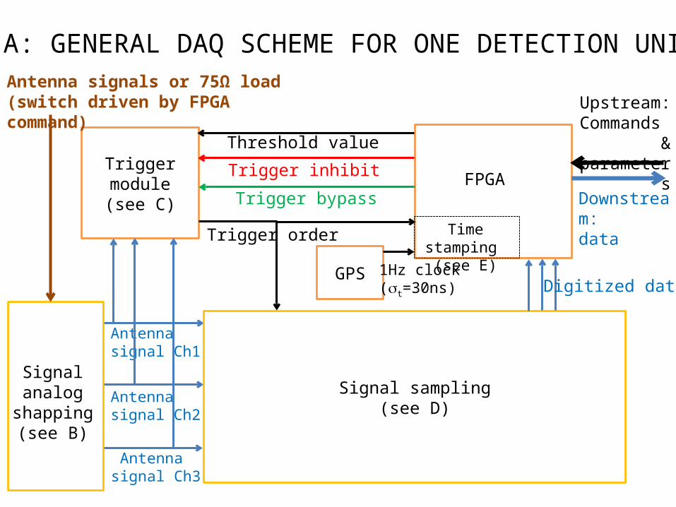
Trigger module(see C)
Trigger inhibit
Trigger bypass
Threshold value
Trigger order
FPGA
Antenna signal Ch1
Antenna signal Ch2
Antenna signal Ch3
Signal analog
shapping(see B)
Signal sampling(see D)
A: GENERAL DAQ SCHEME FOR ONE DETECTION UNITAntenna signals or 75Ω load (switch driven by FPGA command)
Downstream: data
Upstream:Commands
& parameters
Digitized dataGPS 1Hz clock
(st=30ns)
Time stamping (see E)
B: analog shaping
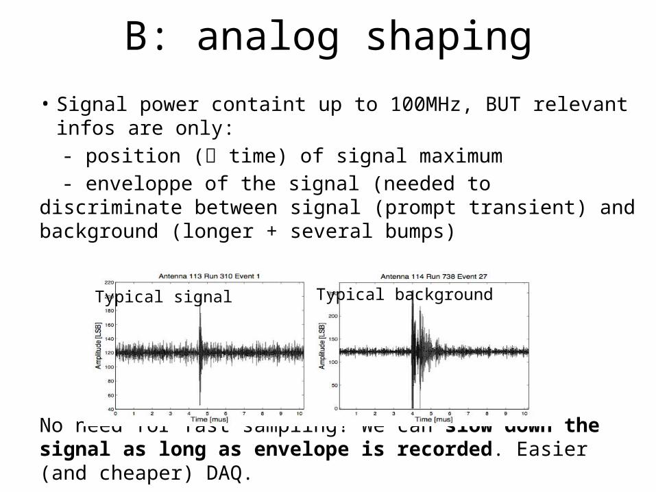
• Signal power containt up to 100MHz, BUT relevant infos are only:
- position ( time) of signal maximum- enveloppe of the signal (needed to discriminate between
signal (prompt transient) and background (longer + several bumps)
No need for fast sampling! We can slow down the signal as long as envelope is recorded. Easier (and cheaper) DAQ.
Typical signal Typical background
B: analog shaping
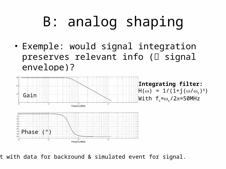
• Exemple: would signal integration preserves relevant info ( signal envelope)?
Integrating filter:H(w) = 1/(1+j(w/wc)4)With fc=wc/2p=50MHz
Test with data for backround & simulated event for signal.
Gain
Phase (°)
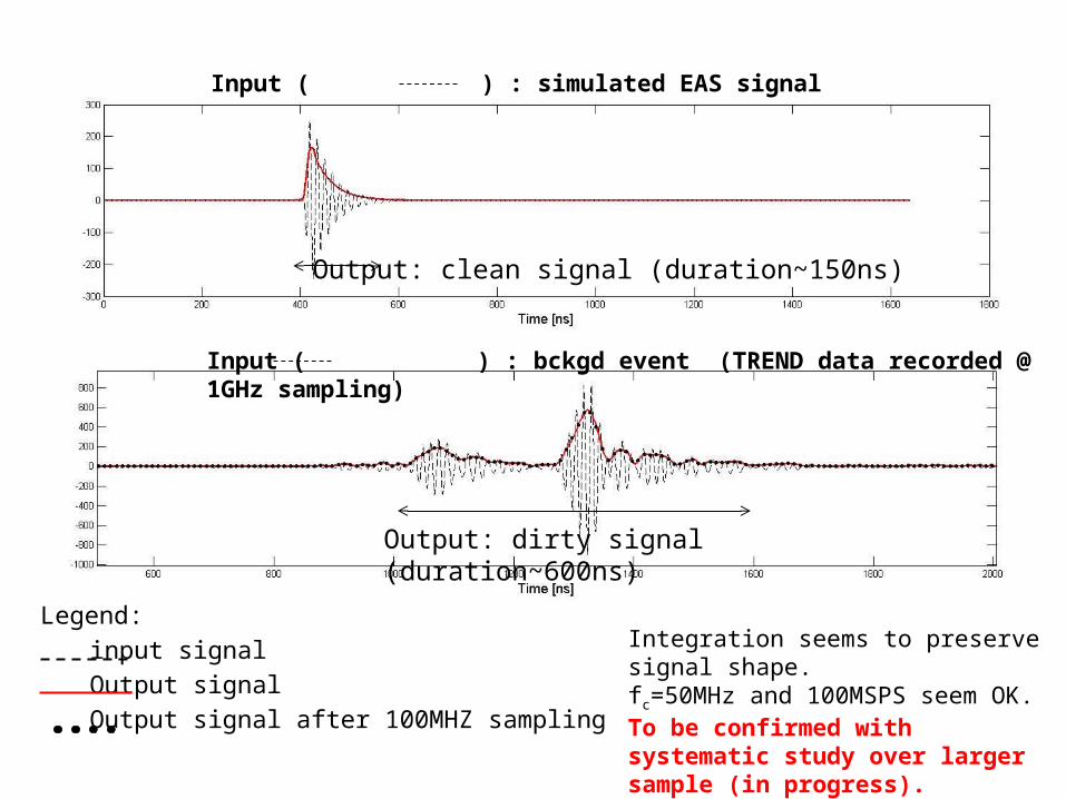
Legend: input signalOutput signalOutput signal after 100MHZ sampling
Output: clean signal (duration~150ns)
Output: dirty signal (duration~600ns)
Input ( ) : bckgd event (TREND data recorded @ 1GHz sampling)
Input ( ) : simulated EAS signal
Integration seems to preserve signal shape.fc=50MHz and 100MSPS seem OK.To be confirmed with systematic study over larger sample (in progress).
B: analog shaping
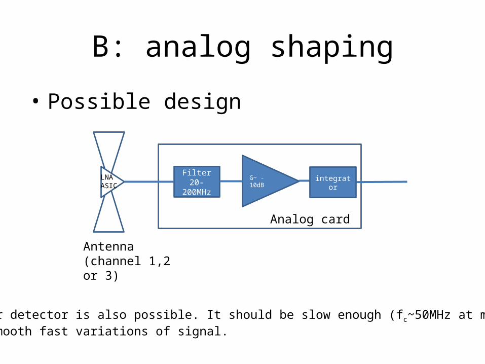
• Possible design
Filter 20-200MHz
G~ -10dB
Analog card
Antenna (channel 1,2 or 3)
integrator
Power detector is also possible. It should be slow enough (fc~50MHz at most) to smooth fast variations of signal.
LNAASIC
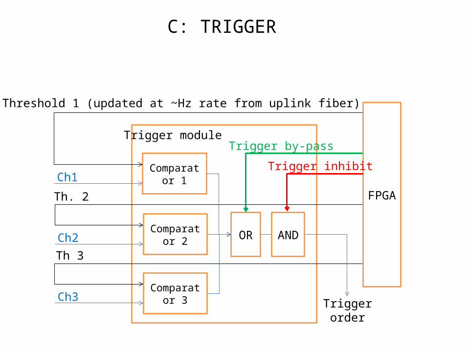
Trigger module
Comparator 1Ch1
Threshold 1 (updated at ~Hz rate from uplink fiber)
ORComparator 2Ch2
Th. 2
Comparator 3Ch3
Th 3
Trigger by-pass
Trigger order
FPGA
AND
Trigger inhibit
C: TRIGGER
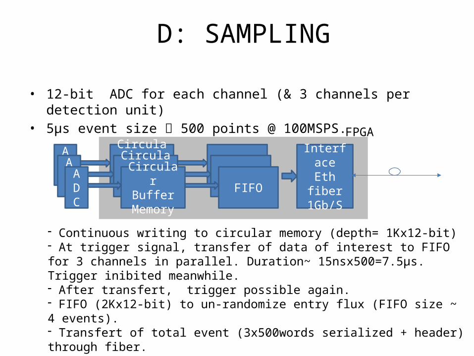
• 12-bit ADC for each channel (& 3 channels per detection unit)• 5µs event size 500 points @ 100MSPS.
ADC
CircularBuffer
MemoryFIFO
- Continuous writing to circular memory (depth= 1Kx12-bit)- At trigger signal, transfer of data of interest to FIFO for 3 channels in parallel. Duration~ 15nsx500=7.5µs. Trigger inibited meanwhile.- After transfert, trigger possible again.- FIFO (2Kx12-bit) to un-randomize entry flux (FIFO size ~ 4 events). - Transfert of total event (3x500words serialized + header) through fiber.
-Expected data rate: 3x500x12bx1000Hz/8 ~ 2.2 MBy/s
ADC
CircularBuffer
MemoryFIFOA
DC
CircularBuffer
MemoryFIFO
Interface Eth fiber
1Gb/S
FPGA
D: SAMPLING
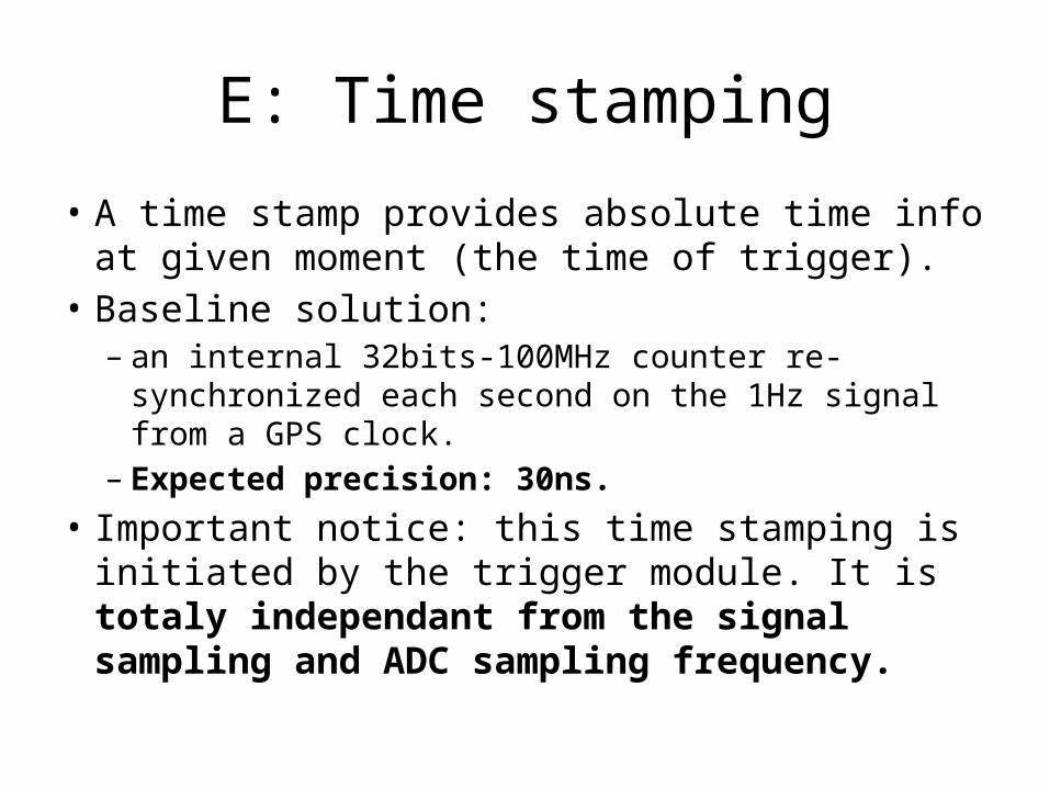
E: Time stamping
• A time stamp provides absolute time info at given moment (the time of trigger).
• Baseline solution: – an internal 32bits-100MHz counter re-synchronized
each second on the 1Hz signal from a GPS clock.– Expected precision: 30ns.
• Important notice: this time stamping is initiated by the trigger module. It is totaly independant from the signal sampling and ADC sampling frequency.
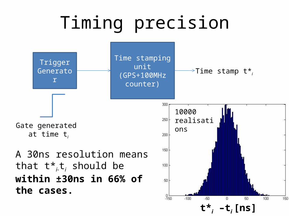
Timing precision
Time stamping unit(GPS+100MHz
counter)
TriggerGenerator
Gate generated at time ti
Time stamp t*i
t*i –ti [ns]
A 30ns resolution means that t*i-ti should be within ±30ns in 66% of the cases.
10000 realisations
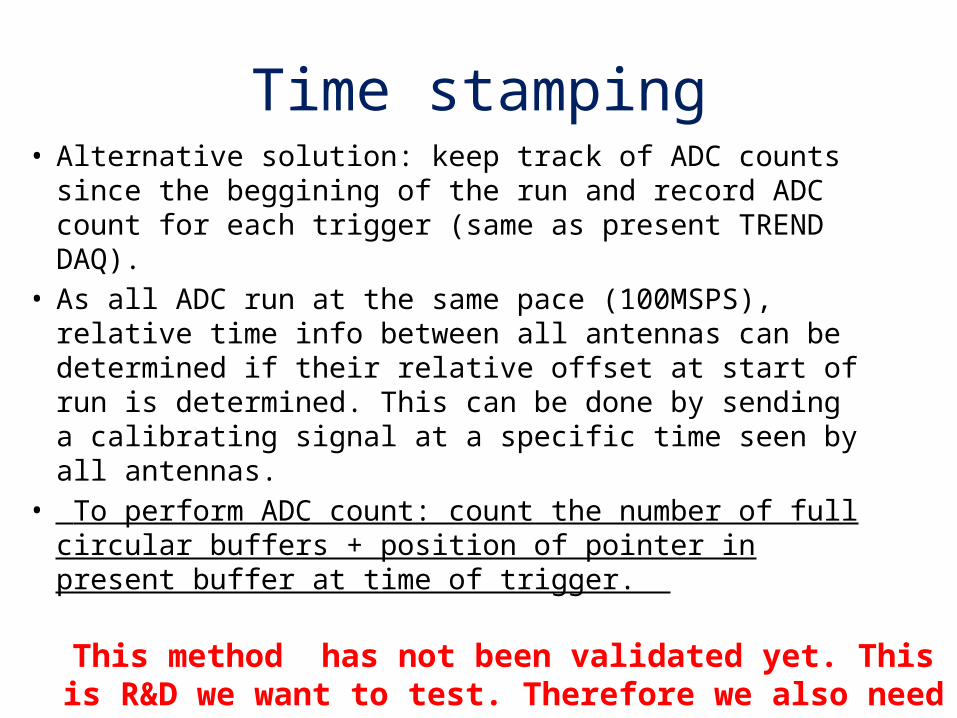
Time stamping• Alternative solution: keep track of ADC counts since the
beggining of the run and record ADC count for each trigger (same as present TREND DAQ).
• As all ADC run at the same pace (100MSPS), relative time info between all antennas can be determined if their relative offset at start of run is determined. This can be done by sending a calibrating signal at a specific time seen by all antennas.
• To perform ADC count: count the number of full circular buffers + position of pointer in present buffer at time of trigger.
This method has not been validated yet. This is R&D we want to test. Therefore we also need GPS method (see before).
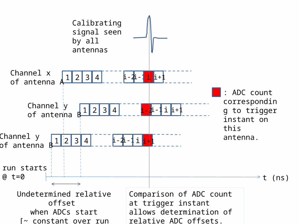
1 2 3 4 i-2 i-1 i i+1Channel xof antenna A
t (ns)
1 2 3 4 i-2 i-1 i i+1Channel yof antenna B
1 2 3 4 i-2 i-1 i i+1Channel yof antenna B
Undetermined relative offset when ADCs start
[~ constant over run duration]
: ADC count corresponding to trigger instant on this antenna.
Calibrating signal seen by all antennas
Comparison of ADC count at trigger instant allows determination of relative ADC offsets.
run starts @ t=0
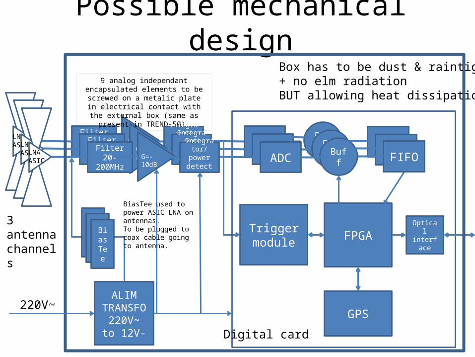
Possible mechanical design
Filter 20-200MHz
9 analog independant encapsulated elements to be screwed on a metalic plate in electrical contact with the external box
(same as present in TREND-50).
Integrator/ power detector
LNAASIC G=15dB ADC FIFOBuff
FPGA
GPS
Trigger module
Optical interface
Filter 20-200MHz
Integrator/ power detector
LNAASIC G=15dB ADC FIFOBuffFilter 20-
200MHz
3 antenna channels
Integrator/ power detector
LNAASIC
G=-10dB ADC FIFOBuff
Digital card
ALIMTRANSFO 220V~ to
12V-
Box has to be dust & raintight+ no elm radiationBUT allowing heat dissipation.
Bias TeeBias
TeeBias Tee
BiasTee used to power ASIC LNA on antennas.To be plugged to coax cable going to antenna.
220V~
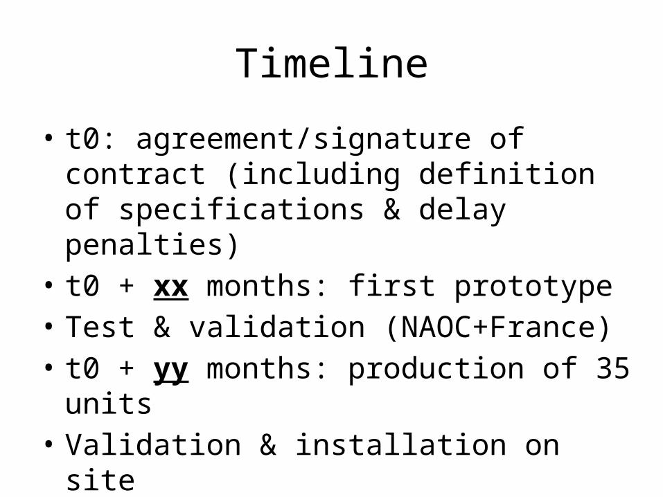
Timeline
• t0: agreement/signature of contract (including definition of specifications & delay penalties)
• t0 + xx months: first prototype• Test & validation (NAOC+France)• t0 + yy months: production of 35 units• Validation & installation on site
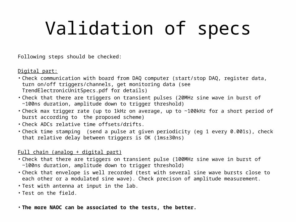
Validation of specsFollowing steps should be checked:
Digital part:• Check communication with board from DAQ computer (start/stop DAQ, register data, turn on/off
triggers/channels, get monitoring data (see TrendElectronicUnitSpecs.pdf for details) • Check that there are triggers on transient pulses (20MHz sine wave in burst of ~100ns duration, amplitude
down to trigger threshold) • Check max trigger rate (up to 1kHz on average, up to ~100kHz for a short period of burst according to the
proposed scheme)• Check ADCs relative time offsets/drifts.• Check time stamping (send a pulse at given periodicity (eg 1 every 0.001s), check that relative delay between
triggers is OK (1ms±30ns)
Full chain (analog + digital part)• Check that there are triggers on transient pulse (100MHz sine wave in burst of ~100ns duration, amplitude
down to trigger threshold)• Check that envelope is well recorded (test with several sine wave bursts close to each other or a modulated
sine wave). Check precison of amplitude measurement.• Test with antenna at input in the lab.• Test on the field.
• The more NAOC can be associated to the tests, the better.
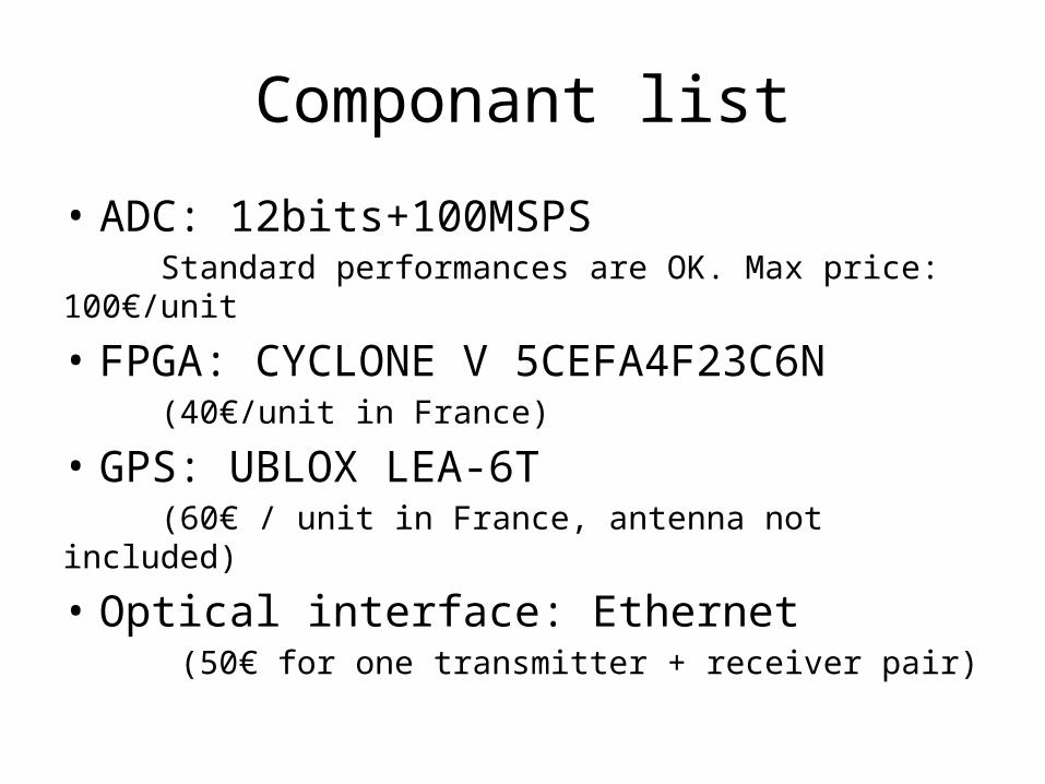
Componant list
• ADC: 12bits+100MSPS Standard performances are OK. Max price: 100€/unit
• FPGA: CYCLONE V 5CEFA4F23C6N (40€/unit in France)
• GPS: UBLOX LEA-6T (60€ / unit in France, antenna not included)
• Optical interface: Ethernet (50€ for one transmitter + receiver pair)
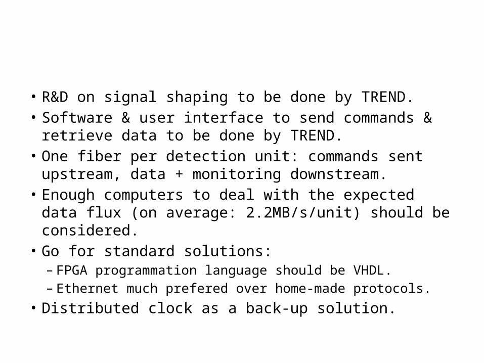
• R&D on signal shaping to be done by TREND.• Software & user interface to send commands & retrieve
data to be done by TREND.• One fiber per detection unit: commands sent upstream,
data + monitoring downstream.• Enough computers to deal with the expected data flux (on
average: 2.2MB/s/unit) should be considered.• Go for standard solutions:
– FPGA programmation language should be VHDL.– Ethernet much prefered over home-made protocols.
• Distributed clock as a back-up solution.