Status of 0 νββ decay experiments Giorgio Gratta Stanford, Physics Dept P5, SLAC Feb 21, 2008
Upload
nguyenminhCategory
view
219download
1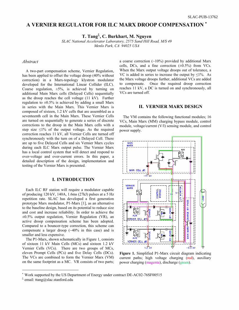
A VERNIER REGULATOR FOR ILC MARX DROOP COMPENSATION ∗
T. Tangξ, C. Burkhart, M. Nguyen SLAC National Accelerator Laboratory, 2575 Sand Hill Road, M/S 49
Menlo Park, CA 94025 USA
∗ Work supported by the US Department of Energy under contract DE-AC02-76SF00515 ξ email: [email protected]
Abstract A two-part compensation scheme, Vernier Regulation, has been applied to offset the voltage droop (40% without correction) in a Marx-topology klystron modulator developed for the International Linear Collider (ILC). Coarse regulation, ±5%, is achieved by turning on additional Main Marx cells (Delayed Cells) sequentially as the droop reaches the cell voltage (11 kV). Further regulation to ±0.5% is achieved by adding a small Marx in series with the Main Marx. This Vernier Marx is composed of sixteen, 1.2 kV cells that are assembled as a seventeenth cell in the Main Marx. These Vernier Cells are turned on sequentially to generate a series of discrete corrections to the droop in the Main Marx cells with a step size ≤1% of the output voltage. As the required correction reaches 11 kV, all Vernier Cells are turned off synchronously with the turn on of a Delayed Cell. There are up to five Delayed Cells and six Vernier Marx cycles during each ILC Marx output pulse. The Vernier Marx has a local control system that will detect and respond to over-voltage and over-current errors. In this paper, a detailed description of the design, implementation and testing of the Vernier Marx is presented.
I. INTRODUCTION Each ILC RF station will require a modulator capable of producing 120 kV, 140A, 1.6ms (27kJ) pulses at a 5 Hz repetition rate. SLAC has developed a first generation prototype Marx modulator, P1-Marx [1], as an alternative to the baseline design, based on its potential to reduce size and cost and increase reliability. In order to achieve the ±0.5% output regulation, Vernier Regulation (VR), an active droop compensation scheme has been adopted. Compared to a bouncer-type correction, this scheme can compensate a larger droop (~40% in this case) and is smaller and less expensive. The P1-Marx, shown schematically in Figure 1, consists of sixteen 11 kV Main Cells (MCs) and sixteen 1.2 kV Vernier Cells (VCs). There are two groups of MCs, eleven Prompt Cells (PCs) and five Delay Cells (DCs). The VCs are combined to form the Vernier Marx (VM) on the same footprint as a MC. VR consists of two parts;
a coarse correction (~10%) provided by additional Marx cells, DCs, and a fine correction (±0.5%) from VCs. When the Marx output voltage droops out of tolerance, a VC is added in series to increase the output by ≤1%. As the Marx voltage droops further, additional VCs are added to compensate. Once the required droop correction reaches 11 kV, a DC is turned on and synchronously, all VCs are turned off.
II. VERNIER MARX DESIGN The VM contains the following functional modules; 16 VCs, Main Marx (MM) charging bypass module, control module, voltage/current (V/I) sensing module, and control power supply.
Figure 1. Simplified P1-Marx circuit diagram indicating current paths; high voltage charging (red), auxiliary power charging (magenta), discharge (green).
SLAC-PUB-13762
The VM is located between the MM and ground. As shown in Figure 1, the MM charging bypass module provides the return path for Marx charging current and auxiliary power. The storage capacitors in each VM cell are charged through the charging switch IGBT and by-pass diode strings. An isolation diode in series with the capacitor prevents current oscillation between cells when the charging switches close. The auxiliary power path to each cell is through the charging switch IGBT string, auxiliary power diode string and isolation diodes. The Vernier Marx auxiliary power, 48 V, is derived from the same -300 V source as the Main Marx. The “common” is referenced to the output of the VM. Closure of a fire switch adds -1.2kV to the output of the Marx. The by-pass diode provides a conduction path for the cells that have not been fired (e.g. Cell #0 in Figure 1). A V/I monitor board measures the output voltage through a 3600:1 resistive divider and output current through a 20 mΩ current viewing resistor. These two signals are delivered to the control board for over voltage/over current protection. The VM, shown in Figure 2, consists of a PCB motherboard on which connectorized, modular components are mounted. The motherboard is supported by a backing frame and equipotential ring like the Main Marx cells. All the VM components are modular to simplify maintenance.
10
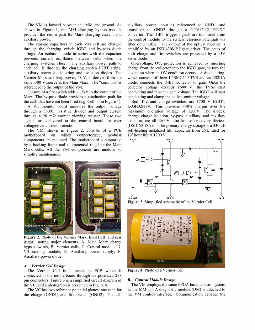
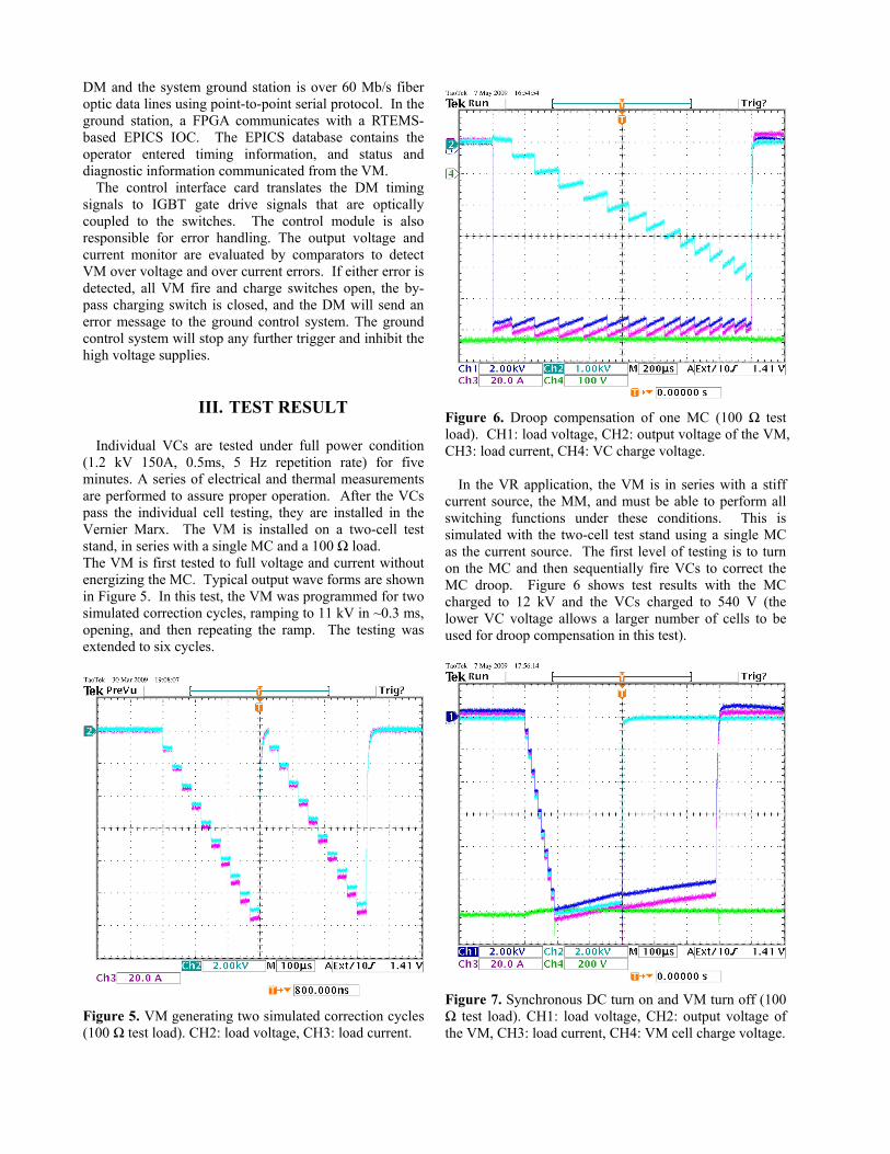
Figure 2. Photo of the Vernier Marx, front (left) and rear (right), noting major elements. A: Main Marx charge bypass switch, B: Vernier cells, C: Control module, D: V/I sensing module, E: Auxiliary power supply, F: Auxiliary power diode. A. Vernier Cell Design The Vernier Cell is a standalone PCB which is connected to the motherboard through six polarized 2x8 pin connectors. Figure 3 is a simplified circuit diagram of the VC, and a photograph is presented in Figure 4. The VC has two reference potential planes; one each for the charge (GND1) and fire switch (GND2). The cell
auxiliary power input is referenced to GND1 and translated to GND2 through a NTV12-12 DC/DC converter. The IGBT trigger signals are translated from the control module to the switch reference potentials via fiber optic cable. The output of the optical receiver is amplified by an IXDI430MYI gate driver. The gates of both charge and fire switches are protected by a 15V
ill start
m capacitor from CSI, rated for 5 hour life at 1200 V.
zener diode. Overvoltage, OV, protection is achieved by injecting charge from the collector into the IGBT gate, to turn the device on when an OV condition occurs. A diode string, which consists of three 1.5SMC440 TVS and an ES2DA diode, connects the IGBT collector to gate. Once the collector voltage exceeds 1600 V, the TVSs start conducting and raise the gate voltage. The IGBT wconducting and clamp the collect-emitter voltage. Both fire and charge switches are 1700 V IGBTs, IXGH32N170. This provides ~40% margin over the maximum operation voltage of 1200V. The diodes; charge, charge isolation, by-pass, auxiliary, and auxiliary isolation, are all 1800V ultra-fast soft-recovery devices (DSDI60-18A). The primary energy storage is a 330 µF self-healing metalized fil
A
C
B B Figure 3. Simplified schematic of the Vernier Cell.
D F E
Figure 4. Photo of a Vernier Cell B. Control Module Design The VM employs the same FPGA based control system as the MM [1]. A diagnostic module (DM) is attached to the VM control interface. Communication between the
DM and the system ground station is over 60 Mb/s fiber optic data lines using point-to-point serial protocol. In the ground station, a FPGA communicates with a RTEMS-based EPICS IOC. The EPICS database contains the operator entered timing information, and status and
p any further trigger and inhibit the high voltage supplies.
III. TEST RESULT
ll test
ating the ramp. The testing was xtended to six cycles.
diagnostic information communicated from the VM. The control interface card translates the DM timing signals to IGBT gate drive signals that are optically coupled to the switches. The control module is also responsible for error handling. The output voltage and current monitor are evaluated by comparators to detect VM over voltage and over current errors. If either error is detected, all VM fire and charge switches open, the by-pass charging switch is closed, and the DM will send an error message to the ground control system. The ground control system will sto
Individual VCs are tested under full power condition (1.2 kV 150A, 0.5ms, 5 Hz repetition rate) for five minutes. A series of electrical and thermal measurements are performed to assure proper operation. After the VCs pass the individual cell testing, they are installed in the Vernier Marx. The VM is installed on a two-cestand, in series with a single MC and a 100 Ω load. The VM is first tested to full voltage and current without energizing the MC. Typical output wave forms are shown in Figure 5. In this test, the VM was programmed for two simulated correction cycles, ramping to 11 kV in ~0.3 ms, opening, and then repee
Figure 5. VM generating two simulated correction cycle
Figure 6. Droop compensation of one MC (100 Ω test load). CH1: load voltage, CH2: output voltage of the VM, CH3: load current, CH4: VC charge voltage. In the VR application, the VM is in series with a stiff current source, the MM, and must be able to perform all switching functions under these conditions. This is simulated with the two-cell test stand using a single MC as the current source. The first level of testing is to turn on the MC and then sequentially fire VCs to correct the MC droop. Figure 6 shows test results with the MC charged to 12 kV and the VCs charged to 540 V (the lower VC voltage allows a larger number of cells to be used for droop compensation in this test).
Figure 7. Synchronous DC turn on and VM turn off (100 Ω test load). CH1: load voltage, CH2: output voltage of the VM, CH3: load current, CH4: VM cell charge voltage.
s (100 Ω test load). CH2: load voltage, CH3: load current.
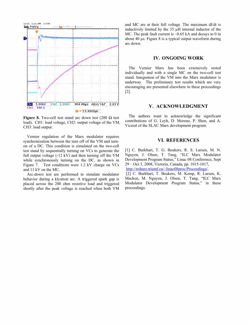
Figure 8. Two-cell test stand arc down test (200 Ω test load). CH1: load voltage, CH2: output voltage of the VM, CH3: load output. Vernier regulation of the Marx modulator requires synchronization between the turn off of the VM and turn-on of a DC. This condition is simulated on the two-cell test stand by sequentially turning on VCs to generate the full output voltage (-12 kV) and then turning off the VM while synchronously turning on the DC, as shown in Figure 7. Test conditions were 1.2 kV charge on VCs and 11 kV on the MC. Arc-down test are performed to simulate modulator behavior during a klystron arc. A triggered spark gap is placed across the 200 ohm resistive load and triggered shortly after the peak voltage is reached when both VM
and MC are at their full voltage. The maximum dI/dt is inductively limited by the 35 µH internal inductor of the MC. The peak fault current is ~0.65 kA and decays to 0 in about 40 µs. Figure 8 is a typical output waveform during arc down.
IV. ONGOING WORK The Vernier Marx has been extensively tested individually and with a single MC on the two-cell test stand. Integration of the VM into the Marx modulator is underway. The preliminary test results which are very encouraging are presented elsewhere in these proceedings [2].
V. ACKNOWLEDGMENT The authors want to acknowledge the significant contributions of G. Leyh, D. Moreno, P. Shen, and A. Viceral of the SLAC Marx development program.
VI. REFERENCES [1] C. Burkhart, T. G. Beukers, R. S. Larsen, M. N. Nguyen, J. Olsen, T. Tang, “ILC Marx Modulator Development Program Status,” Linac 08 Conference, Sept 29 – Oct 3, 2008, Victoria, Canada, pp. 1015-1017, http://trshare.triumf.ca/~linac08proc/Proceedings/. [2] C. Burkhart, T. Beukers, M. Kemp, R. Larsen, K. Macken, M. Nguyen, J. Olsen, T. Tang, “ILC Marx Modulator Development Program Status,” in these proceedings.