
Practical 1 Date: 3ed Jan. Aim: To Study about Microwind...
54
1 Practical 1 Date: 3ed Jan. Aim: To Study about Microwind tool and λ (Lambda) Rules for Layout Generation. Objective: 1. To be familiar with tool. 2. To learn about λ (Lambda) Rules for 90 nm Technology. Microwind Getting Started: The present experiment is a guide to using the « Microwind » educational software on a PC computer. The MICROWIND program allows the student to design and simulate an integrated circuit. The package itself contains a library of common logic and analog ICs to view and simulate. MICROWIND includes all the commands for a mask editor as well as new original tools never gathered before in a single module. You can gain access to Circuit Simulation by pressing one single key. The electric extraction of your circuit is automatically performed and the analog simulator produces voltage and current curves immediately. A specific command displays the characteristics of pMOS and nMOS, where the size of the device and the process parameters can be very easily changed. Altering the MOS model parameters and, then, seeing the effects on the Vds and Ids curves constitutes a good interactive tutorial on devices. The Process Simulator shows the layout in a vertical perspective, as when fabrication has been completed. This feature is a significant aid to supplement the descriptions of fabrication found in most textbooks. The Logic Cell Compiler is a particularly sophisticated tool enabling the automatic design of a CMOS circuit corresponding to your logic description in VERILOG. The DSCH software, which is a user-friendly schematic editor and a logic simulator presented in a companion manual, is used to generate this Verilog description. The cell is created in compliance with the environment, design rules and fabrication specifications. A set of CMOS processes ranging from 1.2μm down to state-of-the-art 0.25μm are proposed. To use the MICROWIND program use the following procedure: Go to the directory in which the software has been copied
Transcript of Practical 1 Date: 3ed Jan. Aim: To Study about Microwind...

1
Practical 1 Date: 3ed Jan.
Aim: To Study about Microwind tool and λ (Lambda) Rules for Layout Generation.
Objective: 1. To be familiar with tool.
2. To learn about λ (Lambda) Rules for 90 nm Technology.
Microwind Getting Started:
The present experiment is a guide to using the « Microwind » educational software on a PC
computer.
The MICROWIND program allows the student to design and simulate an integrated circuit. The
package itself contains a library of common logic and analog ICs to view and simulate.
MICROWIND includes all the commands for a mask editor as well as new original tools never
gathered before in a single module. You can gain access to Circuit Simulation by pressing one
single key. The electric extraction of your circuit is automatically performed and the analog
simulator produces voltage and current curves immediately.
A specific command displays the characteristics of pMOS and nMOS, where the size of the
device and the process parameters can be very easily changed. Altering the MOS model
parameters and, then, seeing the effects on the Vds and Ids curves constitutes a good interactive
tutorial on devices.
The Process Simulator shows the layout in a vertical perspective, as when fabrication has been
completed. This feature is a significant aid to supplement the descriptions of fabrication found in
most textbooks.
The Logic Cell Compiler is a particularly sophisticated tool enabling the automatic design of a
CMOS circuit corresponding to your logic description in VERILOG. The DSCH software, which
is a user-friendly schematic editor and a logic simulator presented in a companion manual, is
used to generate this Verilog description. The cell is created in compliance with the environment,
design rules and fabrication specifications.
A set of CMOS processes ranging from 1.2µm down to state-of-the-art 0.25µm are proposed.
To use the MICROWIND program use the following procedure:
Go to the directory in which the software has been copied
2
(The default directory is MICROWIND)
Double-click on the MicroWind icon
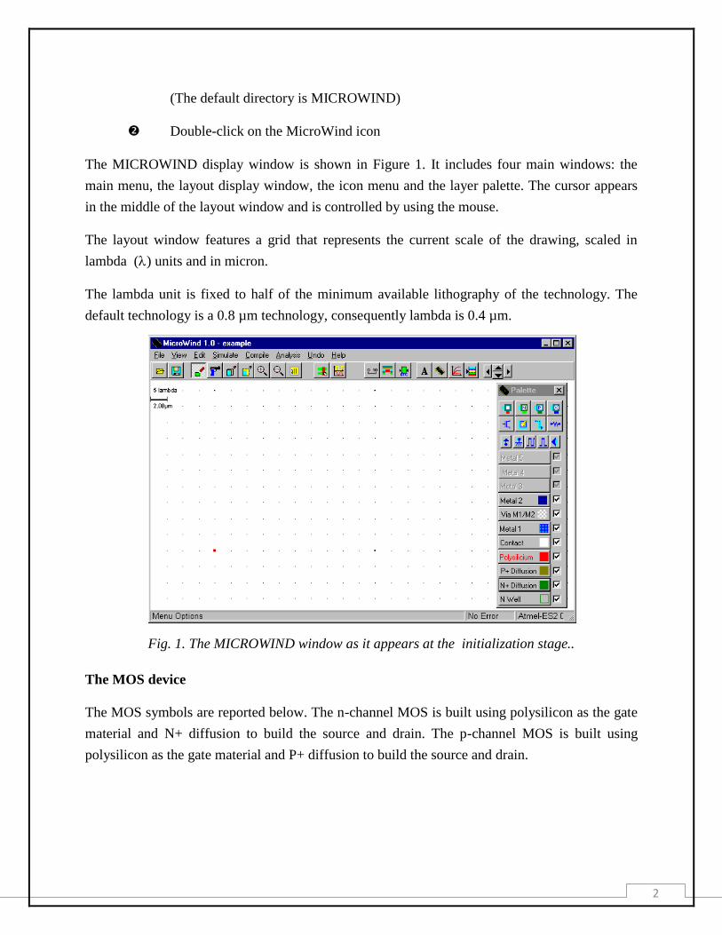
The MICROWIND display window is shown in Figure 1. It includes four main windows: the
main menu, the layout display window, the icon menu and the layer palette. The cursor appears
in the middle of the layout window and is controlled by using the mouse.
The layout window features a grid that represents the current scale of the drawing, scaled in
lambda () units and in micron.
The lambda unit is fixed to half of the minimum available lithography of the technology. The
default technology is a 0.8 µm technology, consequently lambda is 0.4 µm.
Fig. 1. The MICROWIND window as it appears at the initialization stage..
The MOS device
The MOS symbols are reported below. The n-channel MOS is built using polysilicon as the gate
material and N+ diffusion to build the source and drain. The p-channel MOS is built using
polysilicon as the gate material and P+ diffusion to build the source and drain.

3
nMOS pMOS
Manual Design
By using the following procedure, you can create a manual design of the n-channel MOS. The
default icon is the drawing icon shown above. It permits box editing. The display window is
empty. The palette is located in the lower right corner of the screen. A red color indicates the
current layer. Initially the selected layer in the palette is polysilicon. The two first steps are
illustrated in Figure 2.
Fix the first corner of the box with the mouse.
While keeping the mouse button pressed, move the mouse to the
opposite corner of the box.
Release the button. This creates a box in polysilicon layer as shown in Figure 2.
The box width should not be inferior to 2 , which is the minimum width of the
polysilicon box.

4
Fig. 2. Creating a polysilicon box.
Change the current layer into N+ diffusion by a click on the palette of the Diffusion N+ button.
Make sure that the red layer is now the N+ Diffusion. Draw a n-diffusion box at the bottom of
the drawing as in Figure 3. N-diffusion boxes are represented in green. The intersection between
diffusion and polysilicon creates the channel of the nMOS device.
Fig. 3. Creating the N-channel MOS transistor
5
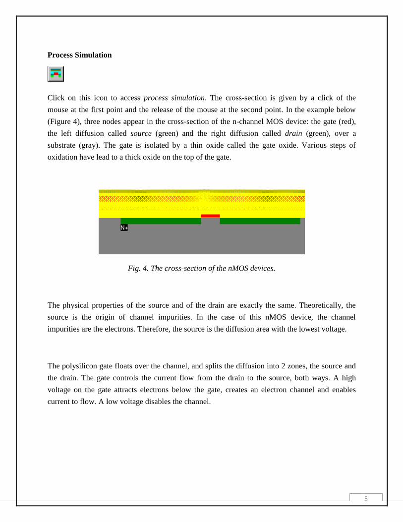
Process Simulation
Click on this icon to access process simulation. The cross-section is given by a click of the
mouse at the first point and the release of the mouse at the second point. In the example below
(Figure 4), three nodes appear in the cross-section of the n-channel MOS device: the gate (red),
the left diffusion called source (green) and the right diffusion called drain (green), over a
substrate (gray). The gate is isolated by a thin oxide called the gate oxide. Various steps of
oxidation have lead to a thick oxide on the top of the gate.
Fig. 4. The cross-section of the nMOS devices.
The physical properties of the source and of the drain are exactly the same. Theoretically, the
source is the origin of channel impurities. In the case of this nMOS device, the channel
impurities are the electrons. Therefore, the source is the diffusion area with the lowest voltage.
The polysilicon gate floats over the channel, and splits the diffusion into 2 zones, the source and
the drain. The gate controls the current flow from the drain to the source, both ways. A high
voltage on the gate attracts electrons below the gate, creates an electron channel and enables
current to flow. A low voltage disables the channel.

6
Mos Characteristics
Click on the MOS characteristics icon. The screen shown in Figure 5 appears. It represents the
Id/Vd simulation of the nMOS device.
Fig. 5. N-Channel MOS characteristics.
The MOS size (width and length of the channel situated at the intersection of the polysilicon gate
and the diffusion) has a strong influence on the value of the current. In Figure 5, the MOS width
is 12.8µm and the length is 1.2µm. Click on OK to return to the editor. A high gate voltage (Vg
=5.0) corresponds to the highest Id/Vd curve. For Vg=0, no current flows. The maximum current
is obtained for Vg=5.0V, Vd=5.0V, with Vs=0.0.
The MOS parameters correspond to SPICE Level 3. You can alter the value of the parameters, or
even access to Level 1. You may also skip to PMOS. You may as well add some measurements
to fit the simulation. Finally, you can simulate devices with other sizes in the proposed list.

7
Add Properties for Simulation
Properties must be added to the layout to activate the MOS device. The most convenient way to
operate the MOS is to apply a clock to the gate, another to the source and to observe the drain.
The summary of available properties is reported below.
VDD property
VSS property
Clock propertyPulse property
Node visible
Apply a clock to the drain. Click on the Clock icon, click on the left diffusion. The Clock
menu appears (See below). Change the name into « drain » and click on OK. A default clock
with 3 ns period is generated. The Clock property is sent to the node and appears at the right
hand side of the desired location with the name « drain ».
Fig. 6. The clock menu.
Apply a clock to the gate. Click on the Clock icon and then, click on
the polysilicon gate. The clock menu appears again.
8
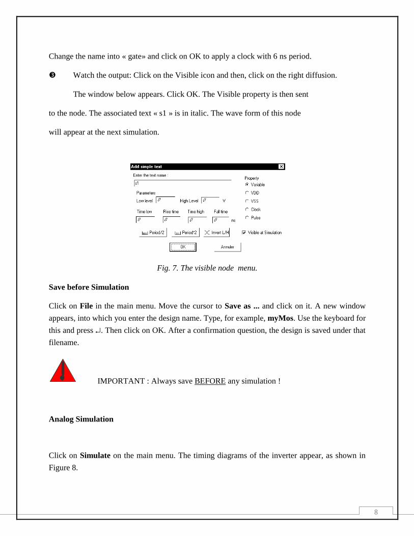
Change the name into « gate» and click on OK to apply a clock with 6 ns period.
Watch the output: Click on the Visible icon and then, click on the right diffusion.
The window below appears. Click OK. The Visible property is then sent
to the node. The associated text « s1 » is in italic. The wave form of this node
will appear at the next simulation.
Fig. 7. The visible node menu.
Save before Simulation
Click on File in the main menu. Move the cursor to Save as ... and click on it. A new window
appears, into which you enter the design name. Type, for example, myMos. Use the keyboard for
this and press . Then click on OK. After a confirmation question, the design is saved under that
filename.
IMPORTANT : Always save BEFORE any simulation !
Analog Simulation
Click on Simulate on the main menu. The timing diagrams of the inverter appear, as shown in
Figure 8.

9
Fig. 8. Analog simulation of the MOS device.
When the gate is at zero, no channel exists so the node s1 is disconnected from the drain. When
the gate is on, the source copies the drain. It can be observed that the nMOS device drives well at
zero but at the high voltage. The final value is 4.2V, that is VDD minus the threshold voltage.
Click on More in order to perform more simulations. Click on Stop to return to the editor.
10
λ (Lambda) Rule:
Design Rules
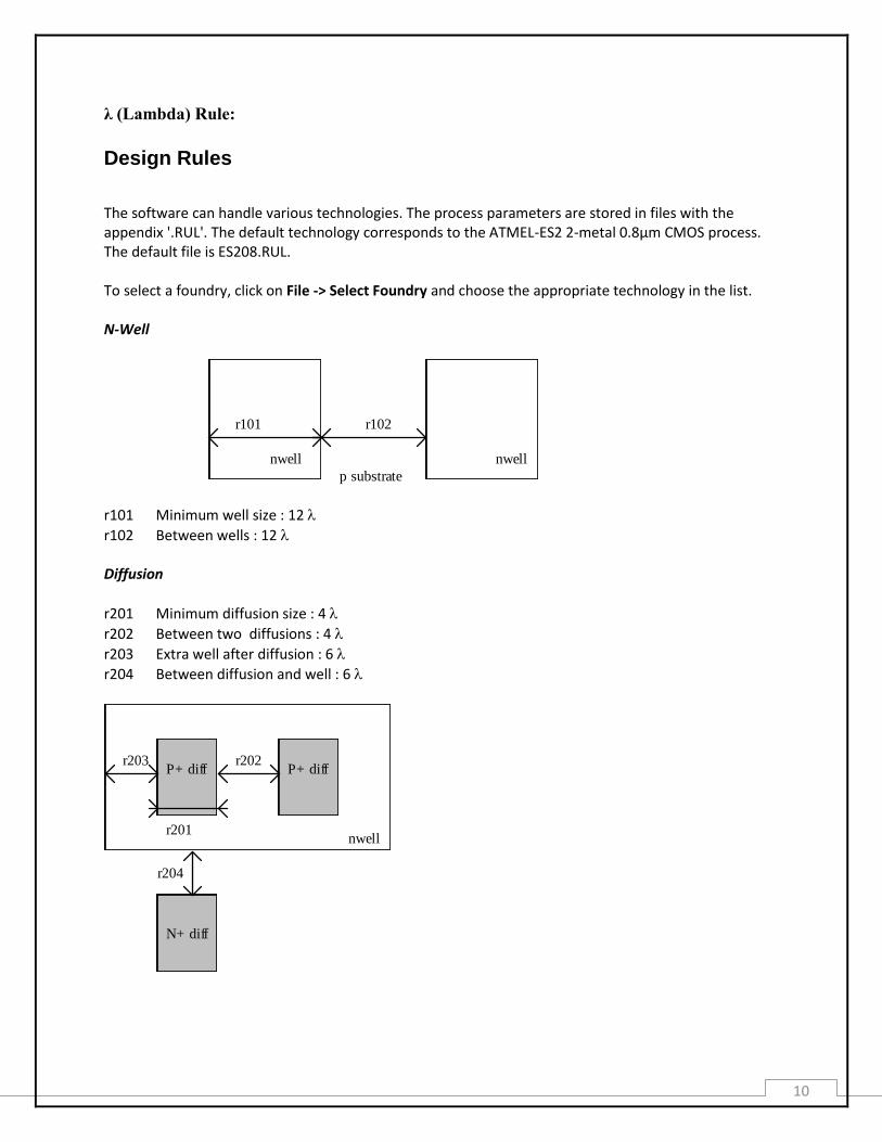
The software can handle various technologies. The process parameters are stored in files with the appendix '.RUL'. The default technology corresponds to the ATMEL-ES2 2-metal 0.8µm CMOS process. The default file is ES208.RUL. To select a foundry, click on File -> Select Foundry and choose the appropriate technology in the list. N-Well
r101 r102
nwell nwell
p substrate
r101 Minimum well size : 12
r102 Between wells : 12 Diffusion
r201 Minimum diffusion size : 4
r202 Between two diffusions : 4
r203 Extra well after diffusion : 6
r204 Between diffusion and well : 6
nwell
P+ diff P+ diff
N+ diff
r204
r202r203
r201
11
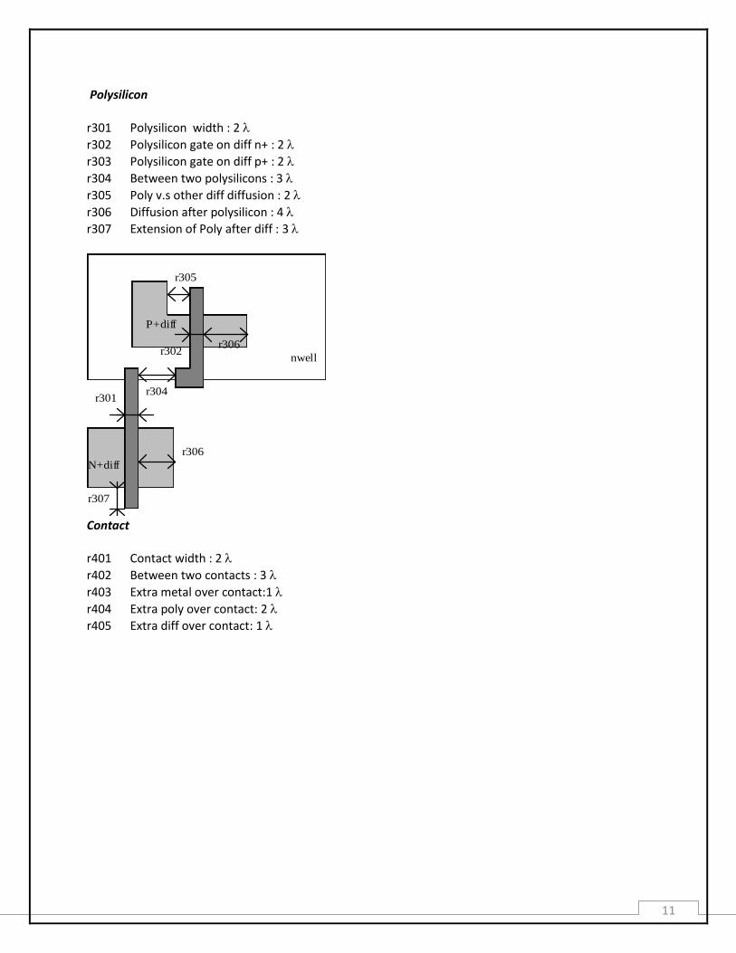
Polysilicon
r301 Polysilicon width : 2
r302 Polysilicon gate on diff n+ : 2
r303 Polysilicon gate on diff p+ : 2
r304 Between two polysilicons : 3
r305 Poly v.s other diff diffusion : 2
r306 Diffusion after polysilicon : 4
r307 Extension of Poly after diff : 3
nwell
P+diff
r305
r302r306
N+diff
r304r301
r306
r307
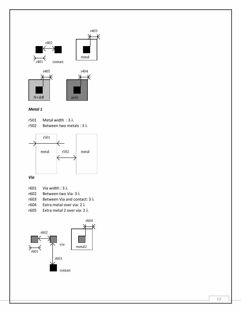
Contact
r401 Contact width : 2
r402 Between two contacts : 3
r403 Extra metal over contact:1
r404 Extra poly over contact: 2
r405 Extra diff over contact: 1
12
r401
r402
contact
metal
r403
N+diff
r405
poly
r404
Metal 1
r501 Metal width : 3
r502 Between two metals : 3
metal
r501
metalr502
Via
r601 Via width : 3
r602 Between two Via: 3
r603 Between Via and contact: 3
r604 Extra metal over via: 2
r605 Extra metal 2 over via: 2
r601
r602
viametal2
r604
contact
r603
13
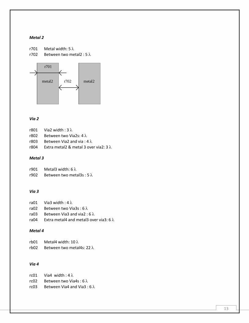
Metal 2
r701 Metal width: 5
r702 Between two metal2 : 5
metal2
r701
metal2r702
Via 2
r801 Via2 width : 3
r802 Between two Via2s: 4
r803 Between Via2 and via : 4
r804 Extra metal2 & metal 3 over via2: 3 Metal 3
r901 Metal3 width: 6
r902 Between two metal3s : 5 Via 3
ra01 Via3 width : 4
ra02 Between two Via3s : 6
ra03 Between Via3 and via2 : 6
ra04 Extra metal4 and metal3 over via3: 6 Metal 4
rb01 Metal4 width: 10
rb02 Between two metal4s: 22 Via 4
rc01 Via4 width : 4
rc02 Between two Via4s : 6
rc03 Between Via4 and Via3 : 6
14
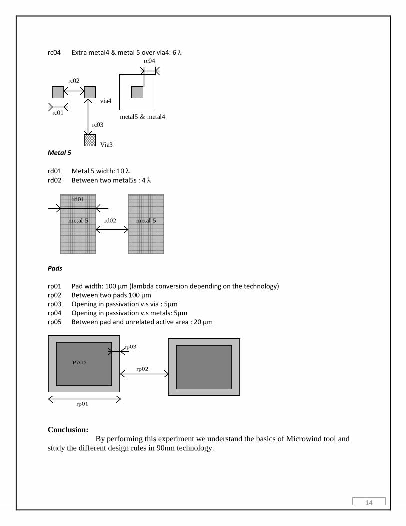
rc04 Extra metal4 & metal 5 over via4: 6
rc01
rc02
via4
metal5 & metal4
rc04
Via3
rc03
Metal 5
rd01 Metal 5 width: 10
rd02 Between two metal5s : 4
metal 5
rd01
metal 5rd02
Pads rp01 Pad width: 100 µm (lambda conversion depending on the technology) rp02 Between two pads 100 µm rp03 Opening in passivation v.s via : 5µm rp04 Opening in passivation v.s metals: 5µm rp05 Between pad and unrelated active area : 20 µm
PAD
rp03
rp01
rp02
Conclusion:
By performing this experiment we understand the basics of Microwind tool and
study the different design rules in 90nm technology.
15
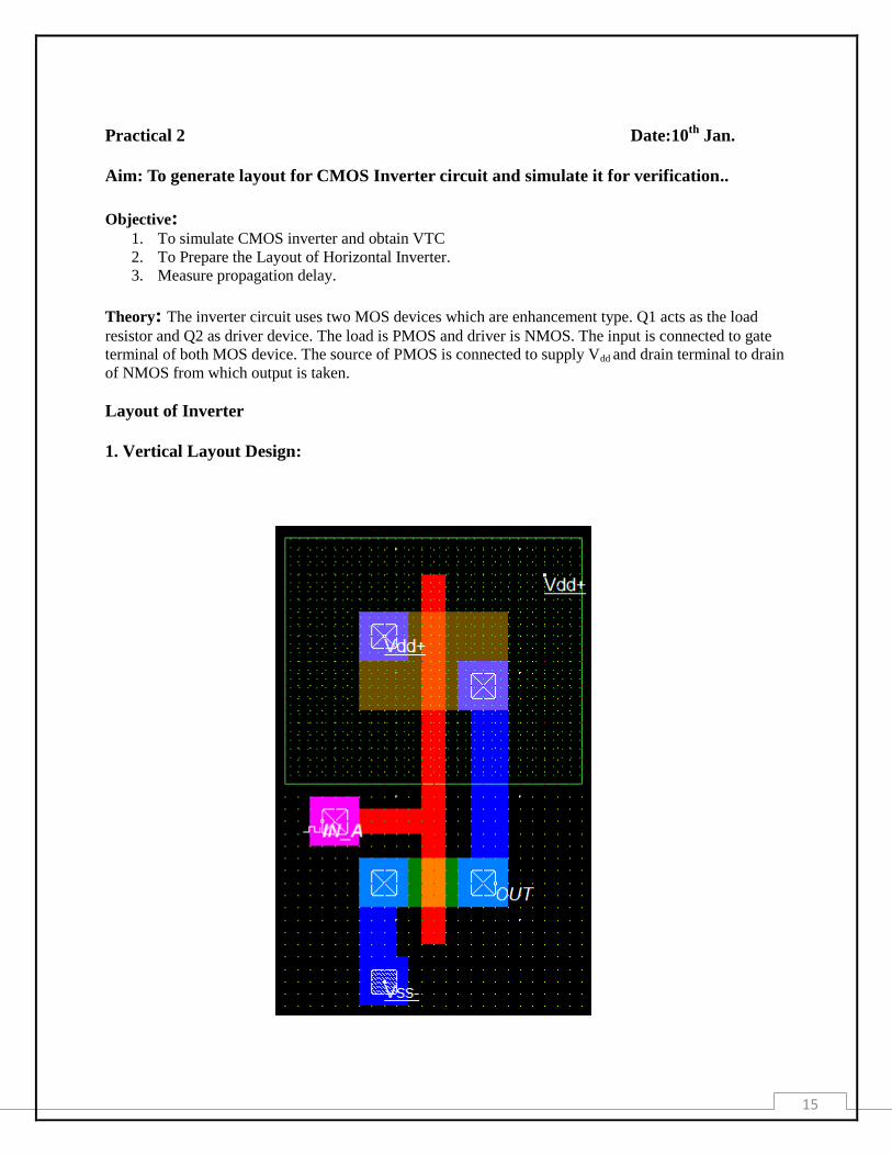
Practical 2 Date:10th
Jan.
Aim: To generate layout for CMOS Inverter circuit and simulate it for verification..
Objective: 1. To simulate CMOS inverter and obtain VTC
2. To Prepare the Layout of Horizontal Inverter.
3. Measure propagation delay.
Theory: The inverter circuit uses two MOS devices which are enhancement type. Q1 acts as the load
resistor and Q2 as driver device. The load is PMOS and driver is NMOS. The input is connected to gate
terminal of both MOS device. The source of PMOS is connected to supply Vdd and drain terminal to drain
of NMOS from which output is taken.
Layout of Inverter
1. Vertical Layout Design:
16
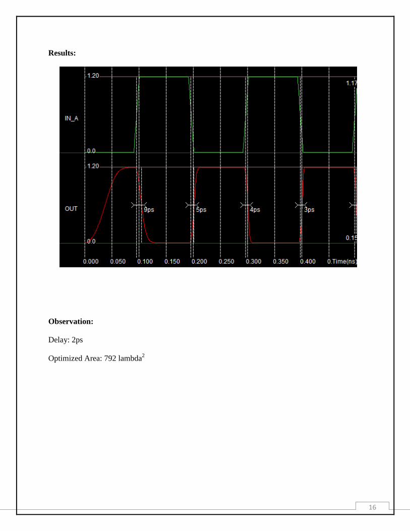
Results:
Observation:
Delay: 2ps
Optimized Area: 792 lambda2
17
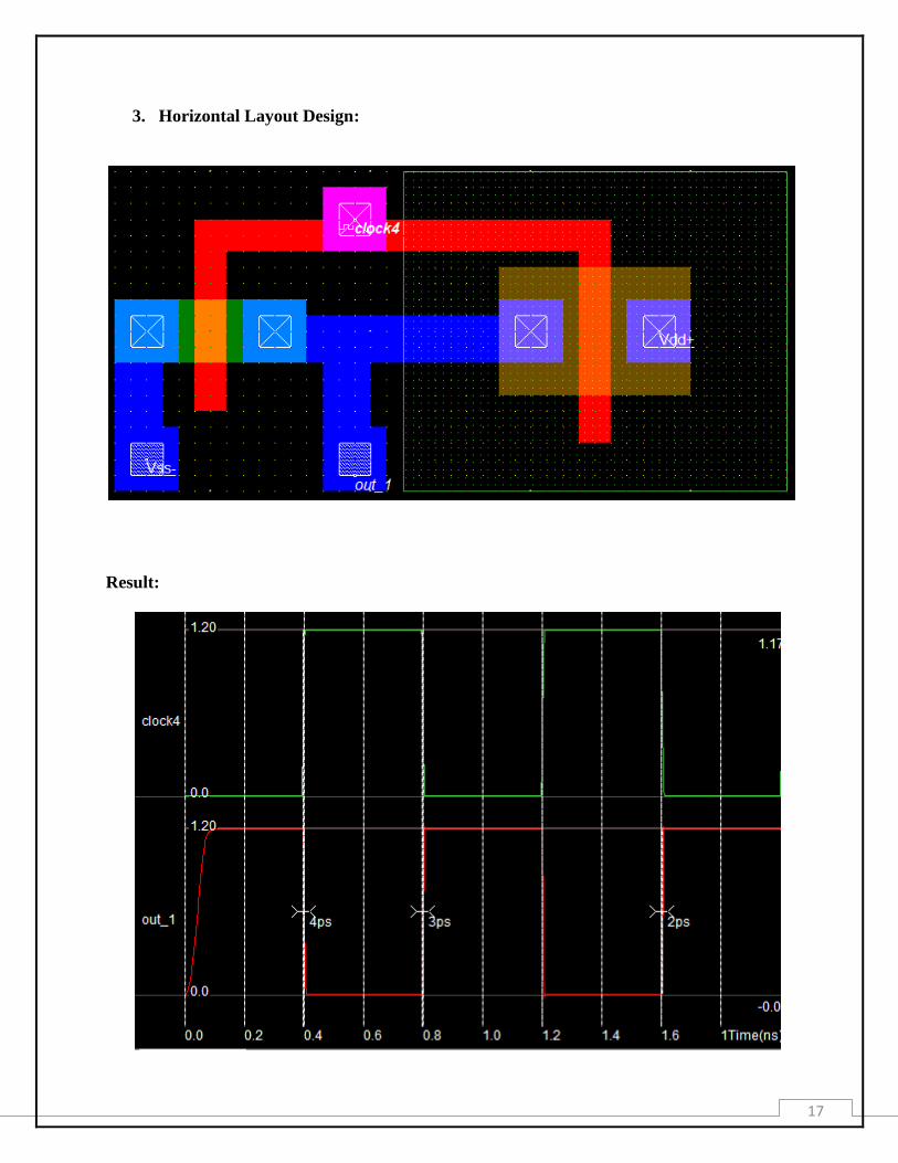
3. Horizontal Layout Design:
Result:
18
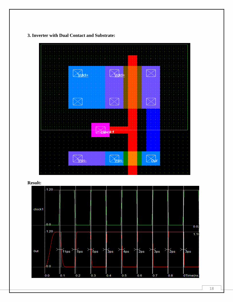
3. Inverter with Dual Contact and Substrate:
Result:
19
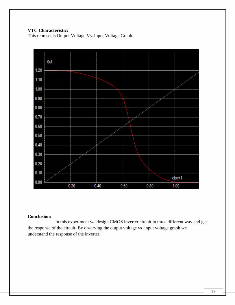
VTC Characteristic:
This represents Output Voltage Vs. Input Voltage Graph.
Conclusion:
In this experiment we design CMOS inverter circuit in three different way and get
the response of the circuit. By observing the output voltage vs. input voltage graph we
understand the response of the inverter.
20
Practical 3 Date: 17th
Jan
Aim: To prepare layout for given logic function and verify it with simulations.
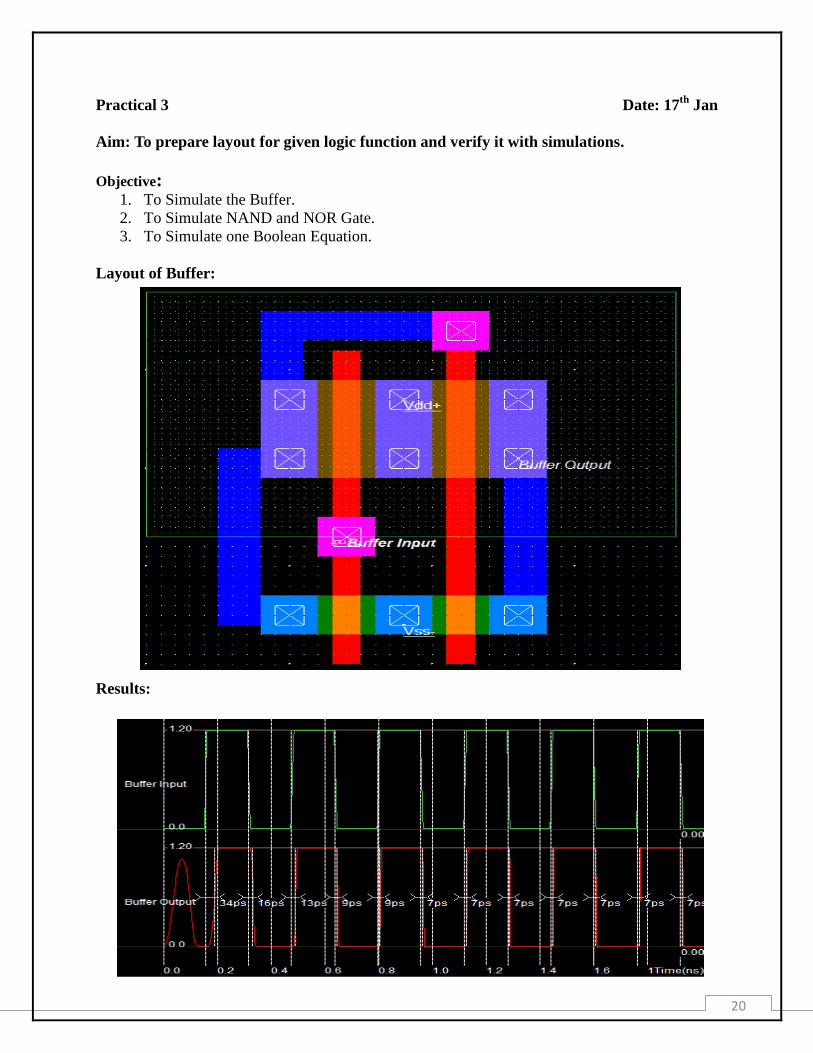
Objective: 1. To Simulate the Buffer.
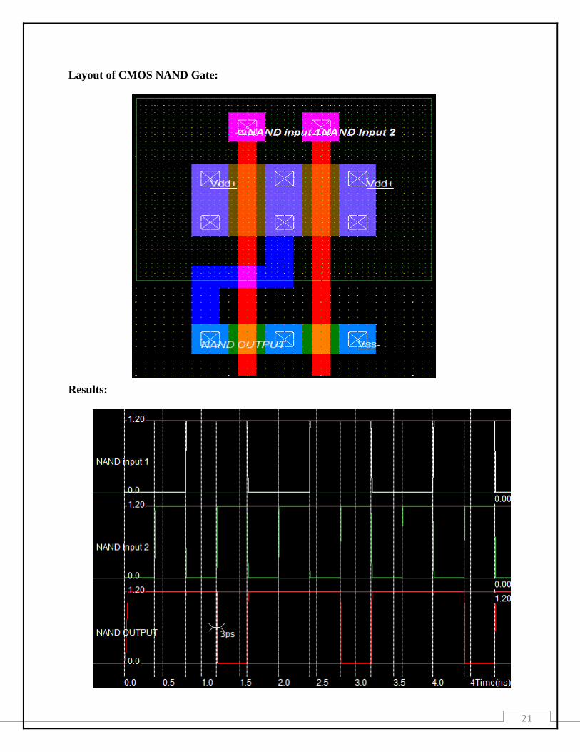
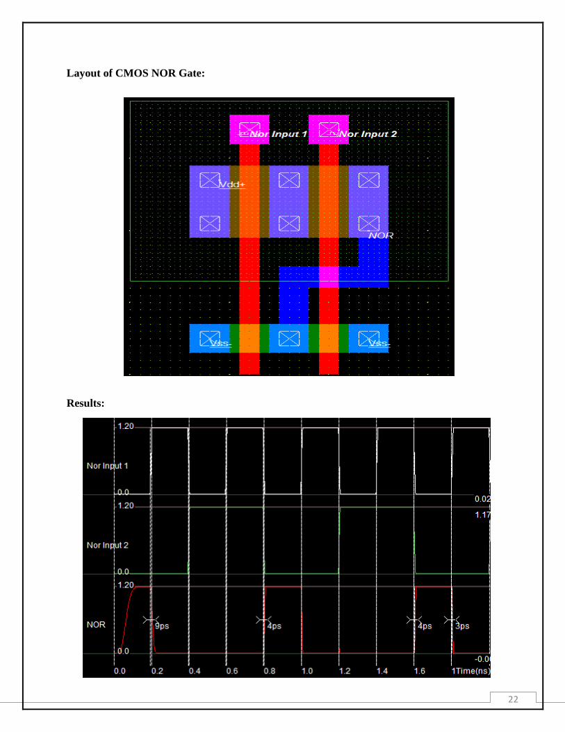
2. To Simulate NAND and NOR Gate.
3. To Simulate one Boolean Equation.
Layout of Buffer:
Results:
21
Layout of CMOS NAND Gate:
Results:
22
Layout of CMOS NOR Gate:
Results:
23
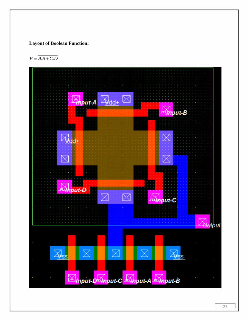
Layout of Boolean Function:
. .F A B C D
24
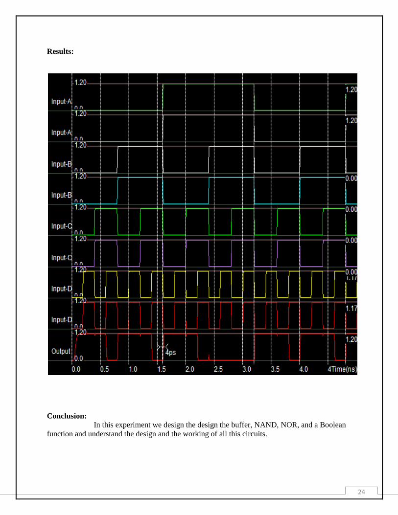
Results:
Conclusion:
In this experiment we design the design the buffer, NAND, NOR, and a Boolean
function and understand the design and the working of all this circuits.
25
Practical 4 Date:31st Jan
Aim: To study about VHDL as first Look.
Objective: 1. To learn Basic about VHDL.
2. To know about VHDL Elements.
Introduction:
VHDL stands for Very high speed integrated circuit Hardware Description Language
Funded by the US Department of Defense in the 70's and 80's
Originally meant for design standardisation, documentation, simulation and ease of
maintenance.
Established as IEEE standard IEEE 1076 in 1987. An updated standard, IEEE 1164 was
adopted in 1993. In 1996 IEEE 1076.3 became a VHDL synthesis standard.
Today VHDL is widely used across the industry for design description, simulation and
synthesis.
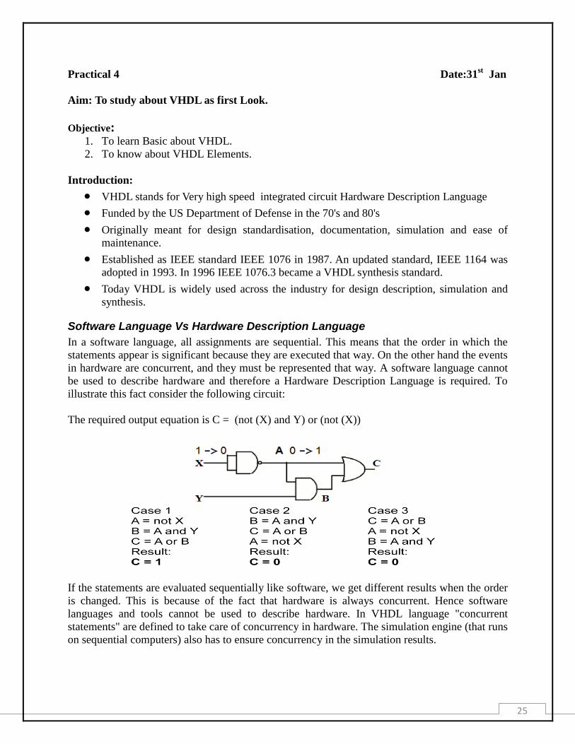
Software Language Vs Hardware Description Language
In a software language, all assignments are sequential. This means that the order in which the
statements appear is significant because they are executed that way. On the other hand the events
in hardware are concurrent, and they must be represented that way. A software language cannot
be used to describe hardware and therefore a Hardware Description Language is required. To
illustrate this fact consider the following circuit:
The required output equation is C = (not (X) and Y) or (not (X))
If the statements are evaluated sequentially like software, we get different results when the order
is changed. This is because of the fact that hardware is always concurrent. Hence software
languages and tools cannot be used to describe hardware. In VHDL language "concurrent
statements" are defined to take care of concurrency in hardware. The simulation engine (that runs
on sequential computers) also has to ensure concurrency in the simulation results.
26
How is concurrency achieved?
One of the requirements for the simulation engine is "order independence" for all concurrent
statements. Thus, if a signal is inverted by process "A", and that signal is read by process "B" at
the same instant of time, it is imperative that process "B" read the old uninverted value. This is
regardless of whether process "A" or process "B" was executed first. This is achieved means of
scheduling. When the simulator tags the signal for an update, it does not perform the update
immediately, but rather remembers the value to be updated. The value is actually updated when
the simulator has finished processing the complete description once.
Features of VHDL:
VHDL is the combination of following languages
- Sequential Language
- Concurrent Language
- Net-List Language
- Simulation Language
- Timing Specifications
- Test Language
Powerful Language Constructs
- e.g. if –then –else / when –else etc.
Design Hierarchies to create modular design
Support for Design Libraries
Portable and Technology independent
VHDL is not case sensitive
VHDL is a free form language. You can write the whole program on a single line.
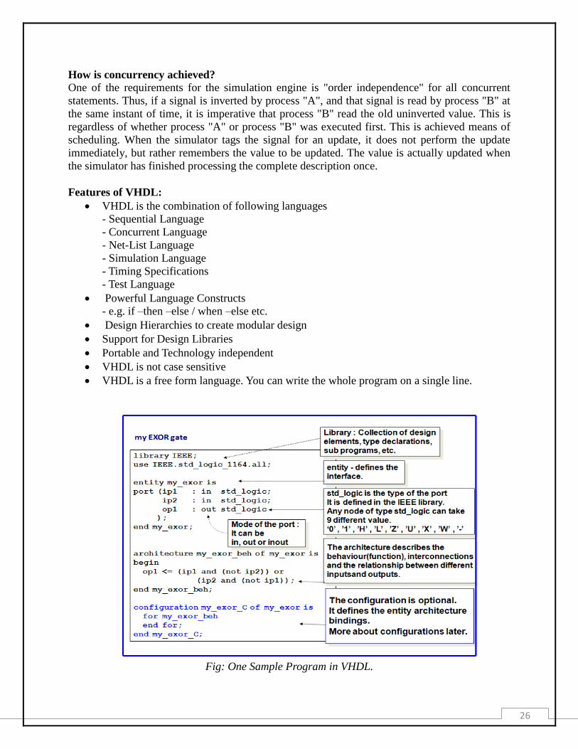
Fig: One Sample Program in VHDL.

27
Quartus II:
Starting New Project:
Open Quartus II
Start Wizard File->New Project Wizard
Click Next , Specify Name of Project and the directory and click Next
Specify files you want to add and click Next
Specify FPGA and click Next , Next and Finish
Cyclone II , EP2C20F484C6
Conclusion:
By performing this experiment we understand the basic conspectus of the VHDL
and the some starting knowledge of the Quartus II.

28
Practical 5 Date: 7st Fab
Aim: Implementation of basic logic gates and its testing.
Objective: 1. First Exposure to VHDL Coding.
2. To Implement the VHDL coding of basic gates.
VHDL Code:
1 ----------library--------------------------------------------- 2 library IEEE; 3 use IEEE.std_logic_1164.all; 4 --------------------------------------------------------------------- 5 ----------entity decleration----------------------------------- 6 entity all_gate is 7 port (a,b: in std_logic; 8 c1,c2,c3,c4,c5,c6,c7,c8: out std_logic); 9 end all_gate; 10 ---------------------------------------------------------------------- 11 --------architecture--------------------------------------------- 12 architecture all_gate_begin of all_gate is 13 begin 14 c1<=(a and b); 15 c2<=a or b; 16 c3<=a nand b; 17 c4<=a nor b; 18 c5<=a xor b; 19 c6<=a xnor b; 20 c7<=not a; 21 c8<=not b; 22 end all_gate_begin; 23 ------------------------------------------------------------------
29
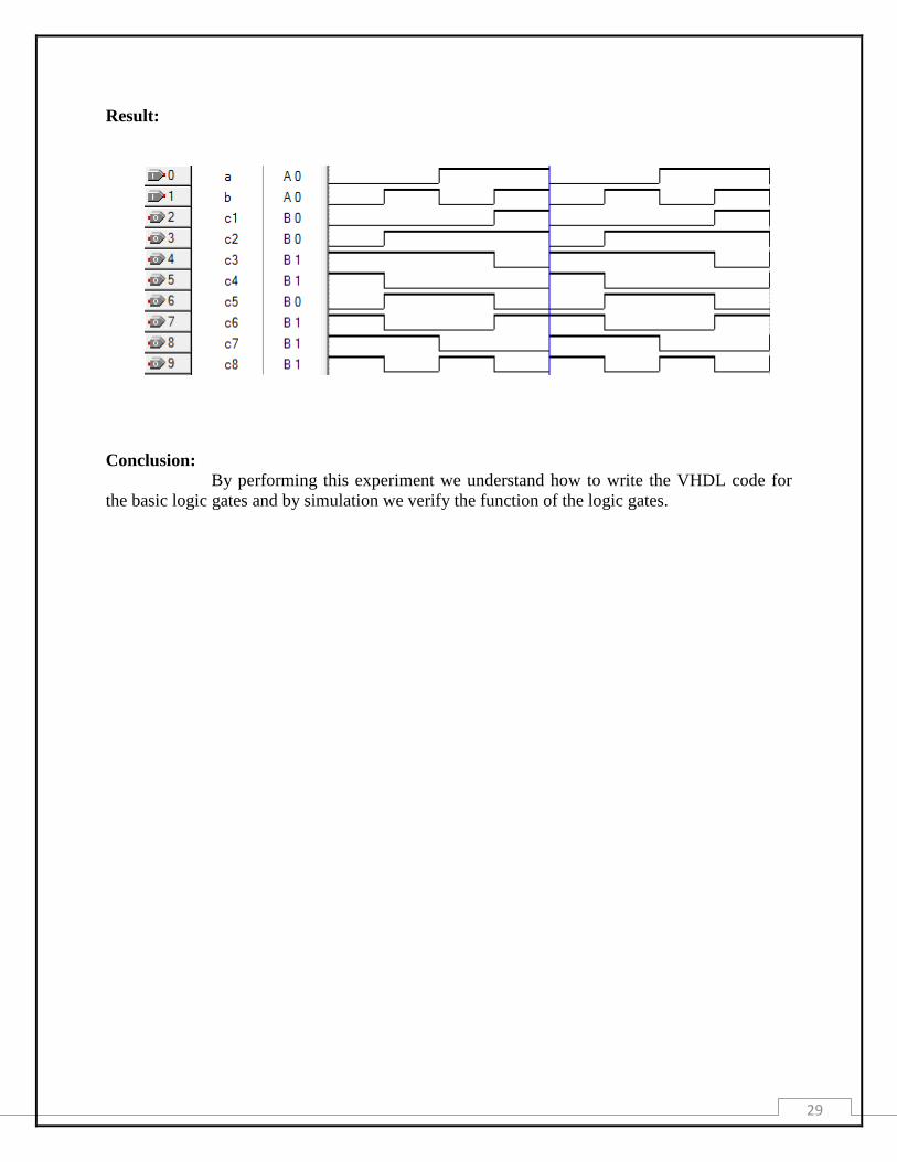
Result:
Conclusion:
By performing this experiment we understand how to write the VHDL code for
the basic logic gates and by simulation we verify the function of the logic gates.
30
Practical 6 Date: 14th
Fab
Aim: Implementation of Adder Circuit and its testing.
Objective: 1. To Implement VHDL Code for Half Adder.
2. To Implement the VHDL Code for Full Adder.
VHDL Code:
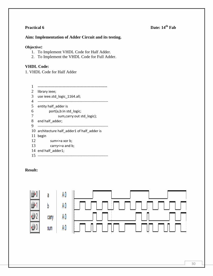
1. VHDL Code for Half Adder
1 --------------------------------------------------
2 library ieee;
3 use ieee.std_logic_1164.all;
4 ------------------------------------------------------------
5 entity half_adder is
6 port(a,b:in std_logic;
7 sum,carry:out std_logic);
8 end half_adder;
9 ------------------------------------------------------------
10 architecture half_adder1 of half_adder is
11 begin
12 sum<=a xor b;
13 carry<=a and b;
14 end half_adder1;
15 ------------------------------------------------------------
Result:
31
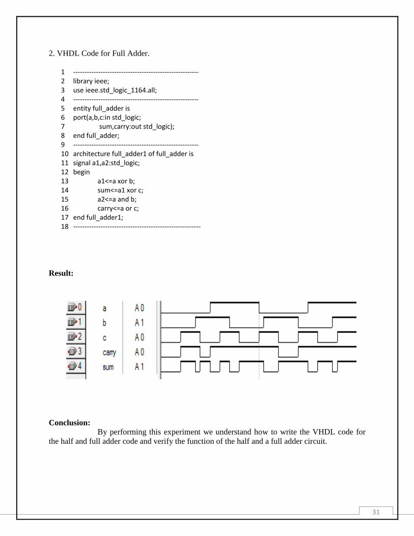
2. VHDL Code for Full Adder.
1 ------------------------------------------------------- 2 library ieee; 3 use ieee.std_logic_1164.all; 4 ------------------------------------------------------- 5 entity full_adder is 6 port(a,b,c:in std_logic; 7 sum,carry:out std_logic); 8 end full_adder; 9 ------------------------------------------------------- 10 architecture full_adder1 of full_adder is 11 signal a1,a2:std_logic; 12 begin 13 a1<=a xor b; 14 sum<=a1 xor c; 15 a2<=a and b; 16 carry<=a or c; 17 end full_adder1; 18 --------------------------------------------------------
Result:
Conclusion:
By performing this experiment we understand how to write the VHDL code for
the half and full adder code and verify the function of the half and a full adder circuit.
32
Practical 7 Date: 21th
Fab.
Aim: Implementation of D Flip Flop and its Testing.
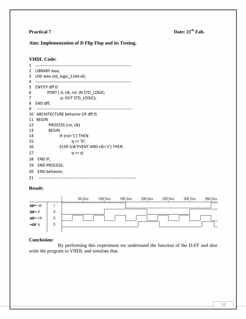
VHDL Code:
1 ----------------------------------------------------------------------- 2 LIBRARY ieee; 3 USE ieee.std_logic_1164.all; 4 ----------------------------------------------------------------------- 5 ENTITY dff IS 6 PORT ( d, clk, rst: IN STD_LOGIC; 7 q: OUT STD_LOGIC); 8 END dff; 9 ----------------------------------------------------------------------- 10 ARCHITECTURE behavior OF dff IS 11 BEGIN 12 PROCESS (rst, clk) 13 BEGIN 14 IF (rst='1') THEN 15 q <= '0'; 16 ELSIF (clk'EVENT AND clk='1') THEN
17 q <= d;
18 END IF;
19 END PROCESS;
20 END behavior;
21 ------------------------------------------------------------------------
Result:
Conclusion:
By performing this experiment we understand the function of the D-FF and also
write the program in VHDL and simulate that.
33
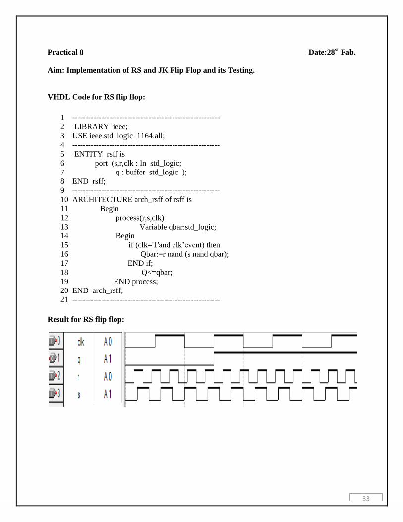
Practical 8 Date:28st Fab.
Aim: Implementation of RS and JK Flip Flop and its Testing.
VHDL Code for RS flip flop:
1 --------------------------------------------------------
2 LIBRARY ieee;
3 USE ieee.std_logic_1164.all;
4 --------------------------------------------------------
5 ENTITY rsff is
6 port (s,r,clk : In std_logic;
7 q : buffer std_logic );
8 END rsff;
9 --------------------------------------------------------
10 ARCHITECTURE arch_rsff of rsff is
11 Begin
12 process(r,s,clk)
13 Variable qbar:std_logic;
14 Begin
15 if (clk='1'and clk’event) then
16 Qbar:=r nand (s nand qbar);
17 END if;
18 Q<=qbar;
19 END process;
20 END arch_rsff;
21 --------------------------------------------------------
Result for RS flip flop:
34
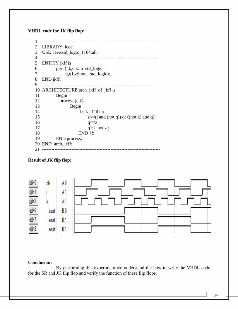
VHDL code for JK flip flop:
1 ---------------------------------------------------------------------------
2 LIBRARY ieee;
3 USE ieee.std_logic_1164.all;
4 ---------------------------------------------------------------------------
5 ENTITY jkff is
6 port (j,k,clk:in std_logic;
7 q,q1,z:inout std_logic);
8 END jkff;
9 ---------------------------------------------------------------------------
10 ARCHITECTURE arch_jkff of jkff is
11 Begin
12 process (clk)
13 Begin
14 if clk='1' then
15 z<=(j and (not q)) or ((not k) and q);
16 q<=z ;
17 q1<=not z ;
18 END if;
19 END process;
20 END arch_jkff;
21 ----------------------------------------------------------------------------
Result of JK flip flop:
Conclusion:
By performing this experiment we understand the how to write the VHDL code
for the SR and JK flip flop and verify the function of these flip flops.

35
Practical 9 Date:21th
Mar.
Aim: Implementation of 4:1 Multiplexer and its Testing.
VHDL Code:
1 ------------------------------------------------------------------
2 LIBRARY ieee;
3 Use ieee.std_logic_1164.all;
4 -------------------------------------------------------------------
5 ENTITY mux is
6 Port ( a,b,c,d,s0,s1 : in std_logic;
7 y : out std_logic );
8 END mux ;
9 --------------------------------------------------------------------
10 ARCHITECTURE arch_mux of mux is
11 Begin
12 Process (a,b,c,d,s0,s1)
13 Variable sel : INTEGER RANGE 0 TO 3;
14 Begin
15 Sel := 0;
16 If (s0 = ’1’) then sel := sel + 1;
17 END if;
18 If (s1 = ’1’) then sel := sel + 2;
19 END if;
20 CASE sel is
21 When 0 => y <=a;
22 When 1 => y <=b;
23 When 2 => y <=c;
24 When 3 => y <=d;
25 END CASE;
26 END process;
27 END arch_mux;
28 --------------------------------------------------------------------------

36
Result:
Conclusion:
By performing this experiment we understand the how to write the VHDL
program for 4:1 multiplexer and by using simulation we verify the function of mux.
37
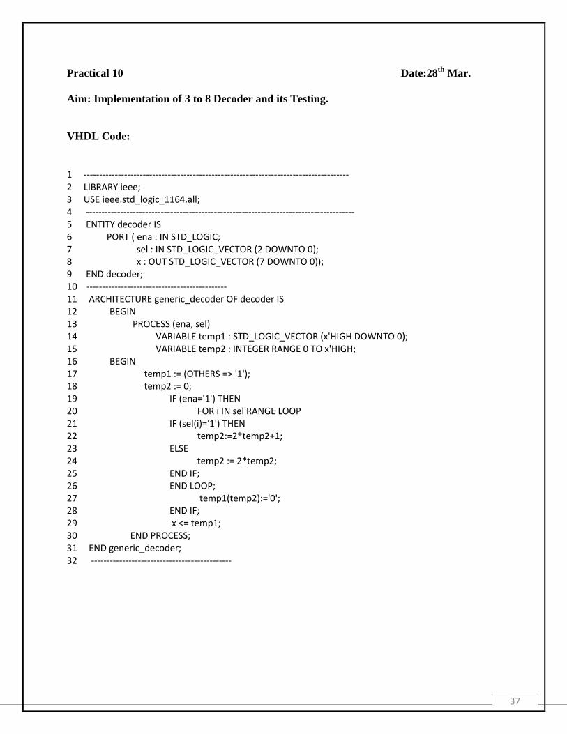
Practical 10 Date:28th
Mar.
Aim: Implementation of 3 to 8 Decoder and its Testing.
VHDL Code:
1 ------------------------------------------------------------------------------------- 2 LIBRARY ieee; 3 USE ieee.std_logic_1164.all; 4 -------------------------------------------------------------------------------------- 5 ENTITY decoder IS 6 PORT ( ena : IN STD_LOGIC; 7 sel : IN STD_LOGIC_VECTOR (2 DOWNTO 0); 8 x : OUT STD_LOGIC_VECTOR (7 DOWNTO 0)); 9 END decoder; 10 --------------------------------------------- 11 ARCHITECTURE generic_decoder OF decoder IS 12 BEGIN 13 PROCESS (ena, sel) 14 VARIABLE temp1 : STD_LOGIC_VECTOR (x'HIGH DOWNTO 0); 15 VARIABLE temp2 : INTEGER RANGE 0 TO x'HIGH; 16 BEGIN 17 temp1 := (OTHERS => '1'); 18 temp2 := 0; 19 IF (ena='1') THEN 20 FOR i IN sel'RANGE LOOP 21 IF (sel(i)='1') THEN 22 temp2:=2*temp2+1; 23 ELSE 24 temp2 := 2*temp2; 25 END IF; 26 END LOOP; 27 temp1(temp2):='0'; 28 END IF; 29 x <= temp1; 30 END PROCESS; 31 END generic_decoder; 32 ---------------------------------------------
38
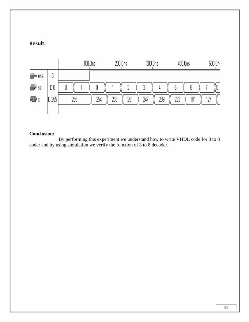
Result:
Conclusion:
By performing this experiment we understand how to write VHDL code for 3 to 8
coder and by using simulation we verify the function of 3 to 8 decoder.

39
Practical 11 Date:04st Apr
Aim: Implementation of BCD Counter and its Testing.
VHDL Code:
1 ----------------------------------------------------------------------------------------------------- 2 LIBRARY ieee; 3 USE ieee.std_logic_1164.all; 4 ---------------------------------------------------------------------------------------------------- 5 ENTITY counter IS 6 PORT ( clk, rst: IN STD_LOGIC; 7 count: OUT STD_LOGIC_VECTOR (3 DOWNTO 0)); 8 END counter; 9 --------------------------------------------------------------------------------------------------- 10 ARCHITECTURE state_machine OF counter IS 11 TYPE state IS (zero, one, two, three, four, 12 five, six, seven, eight, nine); 13 SIGNAL pr_state, nx_state: state; 14 BEGIN 15 ------------- Lower section: ----------------------------------------------------------------- 16 PROCESS (rst, clk) 17 BEGIN 18 IF (rst='1') THEN 19 pr_state <= zero; 20 ELSIF (clk'EVENT AND clk='1') THEN 21 pr_state <= nx_state; 22 END IF; 23 END PROCESS; 24 ------------- Upper section: ------------------------------------------------------------------ 25 PROCESS (pr_state) 26 BEGIN 27 CASE pr_state IS 28 WHEN zero => 29 count <= "0000"; 30 nx_state <= one; 31 WHEN one => 32 count <= "0001"; 33 nx_state <= two; 34 WHEN two => 35 count <= "0010"; 36 nx_state <= three; 37 WHEN three => 38 count <= "0011"; 39 nx_state <= four; 40 WHEN four =>

40
41 count <= "0100"; 42 nx_state <= five; 43 WHEN five => 44 count <= "0101"; 45 nx_state <= six; 46 WHEN six => 47 count <= "0110"; 48 nx_state <= seven; 49 WHEN seven => 50 count <= "0111"; 51 nx_state <= eight; 52 WHEN eight => 53 count <= "1000"; 54 nx_state <= nine; 55 WHEN nine => 56 count <= "1001"; 57 nx_state <= zero; 58 END CASE; 59 END PROCESS; 60 END state_machine;
61 -----------------------------------------------------------------------------------------
Result:
Conclusion:
By performing this experiment we understand how to write VHDL code for the
BCD counter circuit and by using simulation we verify the function of the BCD counter.
41
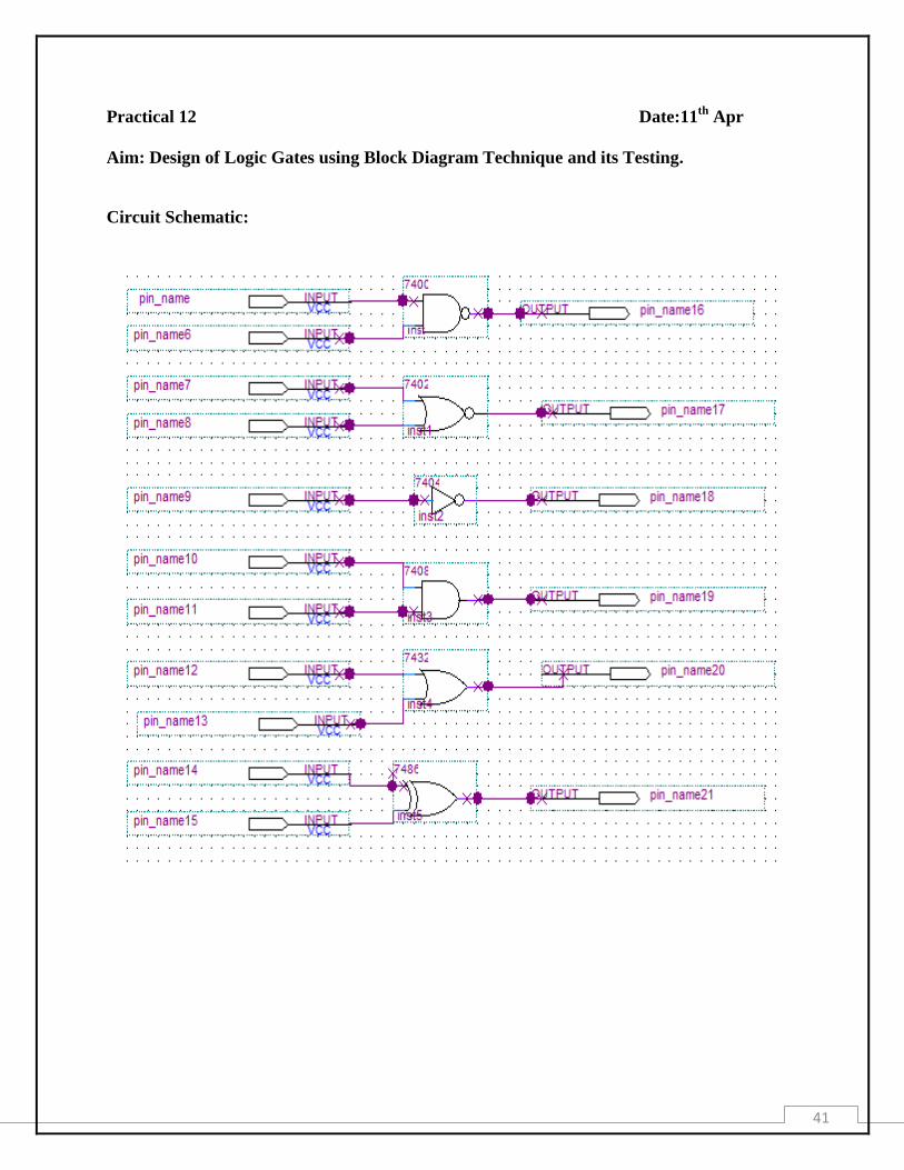
Practical 12 Date:11th
Apr
Aim: Design of Logic Gates using Block Diagram Technique and its Testing.
Circuit Schematic:
42
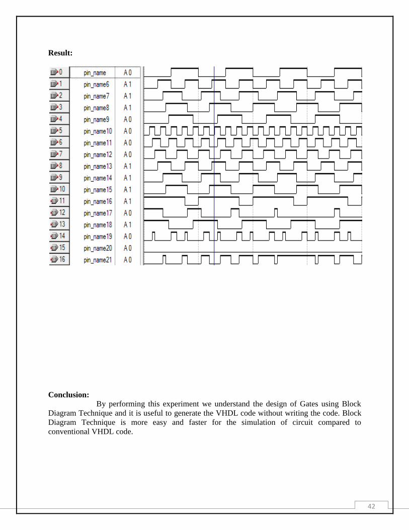
Result:
Conclusion:
By performing this experiment we understand the design of Gates using Block
Diagram Technique and it is useful to generate the VHDL code without writing the code. Block
Diagram Technique is more easy and faster for the simulation of circuit compared to
conventional VHDL code.
43
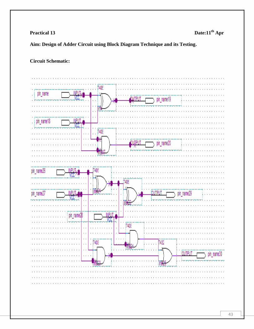
Practical 13 Date:11th
Apr
Aim: Design of Adder Circuit using Block Diagram Technique and its Testing.
Circuit Schematic:

44
Result:
Conclusion:
By performing this experiment we understand the design of adder circuit using
block diagram technique and we verify the function of adder circuit.
45
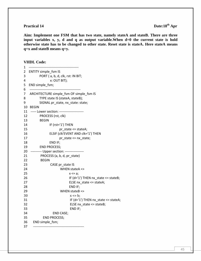
Practical 14 Date:18th
Apr
Aim: Implement one FSM that has two state, namely stateA and stateB. There are three
input variables x, y, d and q as output variable.When d=0 the current state is hold
otherwise state has to be changed to other state. Reset state is stateA. Here stateA means
q=x and stateB means q=y.
VHDL Code:
1 --------------------------------------------- 2 ENTITY simple_fsm IS 3 PORT ( a, b, d, clk, rst: IN BIT; 4 x: OUT BIT); 5 END simple_fsm; 6 ---------------------------------------------- 7 ARCHITECTURE simple_fsm OF simple_fsm IS 8 TYPE state IS (stateA, stateB); 9 SIGNAL pr_state, nx_state: state; 10 BEGIN 11 ----- Lower section: ---------------------- 12 PROCESS (rst, clk) 13 BEGIN 14 IF (rst='1') THEN 15 pr_state <= stateA; 16 ELSIF (clk'EVENT AND clk='1') THEN 17 pr_state <= nx_state; 18 END IF; 19 END PROCESS; 20 ---------- Upper section: ----------------- 21 PROCESS (a, b, d, pr_state) 22 BEGIN 23 CASE pr_state IS 24 WHEN stateA => 25 x <= a; 26 IF (d='1') THEN nx_state <= stateB; 27 ELSE nx_state <= stateA; 28 END IF; 29 WHEN stateB => 30 x <= b; 31 IF (d='1') THEN nx_state <= stateA; 32 ELSE nx_state <= stateB; 33 END IF; 34 END CASE; 35 END PROCESS; 36 END simple_fsm; 37 ----------------------------------------------

46
Result:
Conclusion:
By performing this experiment we understand that how to write the VHDL code
for Finite State Machine (FSM) and we verify the simulation of the circuit.
47
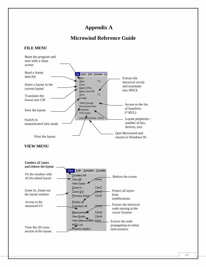
Appendix A
Microwind Reference Guide
FILE MENU
Reset the program and
start with a clean
screen
Read a layout
data file
Insert a layout in the
current layout
Translates the
layout into CIF
Extract the
electrical circuit
and translates
into SPICE
Save the layout
Access to the list
of foundries
(*.RUL)
Switch to
monochrom/Color mode
Layout properties :
number of box,
devices, size
Print the layoutQuit Microwind and
returns to Windows 95
VIEW MENU
Unselect all layers
and redraw the layout
Unselect all layers
and redraw the layout
Fit the window with
all the edited layout
Zoom In, Zoom out
the layout window
Access to the
measured I/V
Extract the node
propagating on metal
interconnectsView the 2D cross-
section of the layout
Redraw the screen
Extract the electrical
node starting at the
cursor location
Protect all layers
from
modifications
48
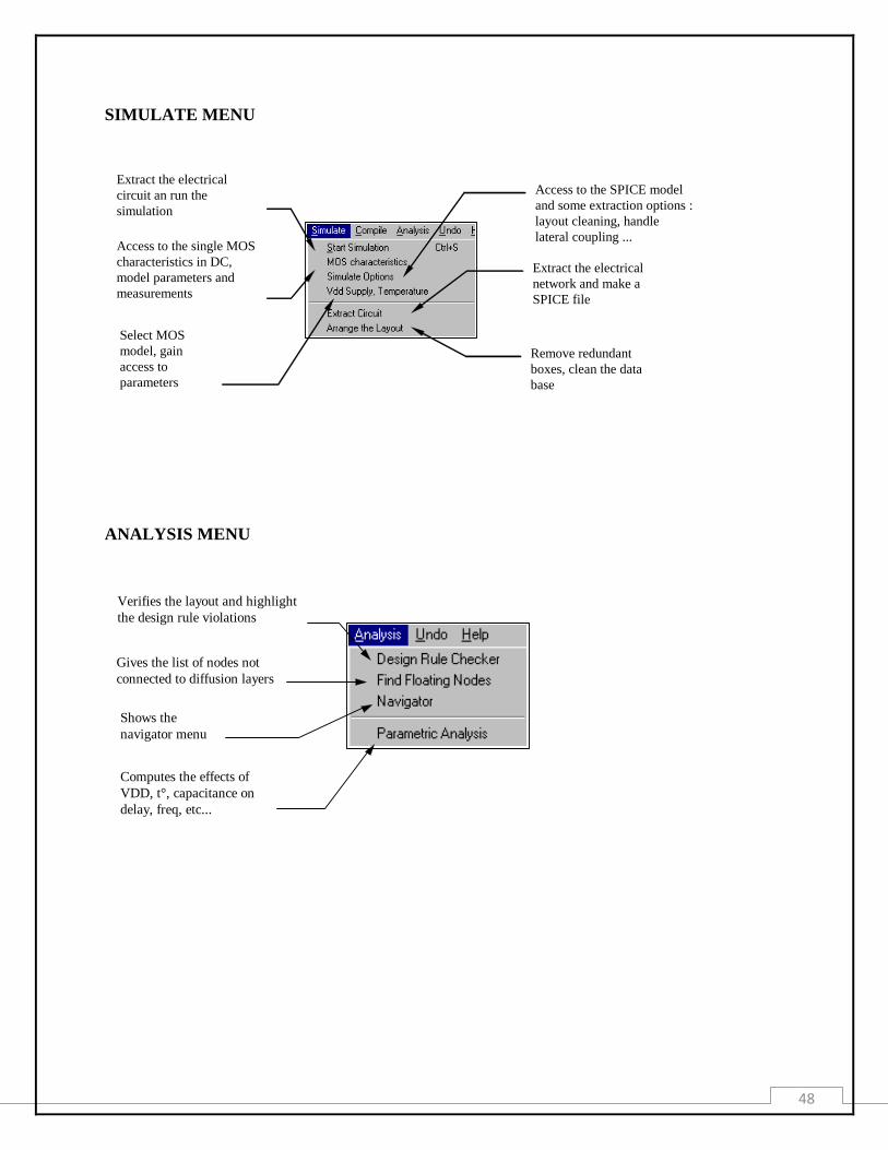
SIMULATE MENU
Extract the electrical
circuit an run the
simulation
Access to the single MOS
characteristics in DC,
model parameters and
measurements
Select MOS
model, gain
access to
parameters
Extract the electrical
network and make a
SPICE file
Access to the SPICE model
and some extraction options :
layout cleaning, handle
lateral coupling ...
Remove redundant
boxes, clean the data
base
ANALYSIS MENU
Verifies the layout and highlight
the design rule violations
Gives the list of nodes not
connected to diffusion layers
Shows the
navigator menu
Computes the effects of
VDD, t°, capacitance on
delay, freq, etc...
49
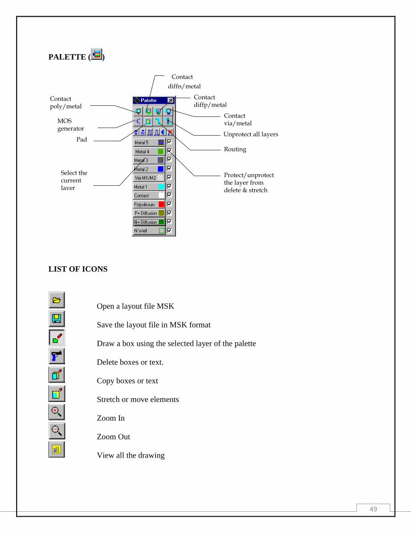
PALETTE ( )
LIST OF ICONS
Open a layout file MSK
Save the layout file in MSK format
Draw a box using the selected layer of the palette
Delete boxes or text.
Copy boxes or text
Stretch or move elements
Zoom In
Zoom Out
View all the drawing
Contactpoly/metal
Contact
diffn/metal
Contactdiffp/metal
Pad
MOSgenerator
Routing
Contactvia/metal
Unprotect all layers
Select thecurrentlayer
Protect/unprotectthe layer fromdelete & stretch

50
Extract and view the electrical node pointed by the cursor
Extract and simulate the circuit
Measure the distance in lambda and micron between two points
2D vertical aspect of the device
Design rule checking of the circuit. Errors are notified in the layout.
Add a text to the layout. The text may include simulation properties.
Chip library of contacts, MOS, metal path, 2-metal routing, pads, etc...
View the palette
Static MOS characteristics
LIST OF FILES
PROGRAM DESCRIPTION
MICROWIND.EXE Layout Editor and Simulator
*.RUL Design rule files
*.MSK Layout files
*.MES MOS I/V Measurements
*.CIR Spice compatible files
*.TXT Verilog text inputs
*.RUL The MICROWIND program reads the rule file to update the simulator parameters (Vt,
K,VDD, etc...), the design rules and parasitic capacitor values. A detailed description of the
.RUL file is reported at the end of Chapter 8.
*.MSK The MICROWIND software creates data files with the appendix .MSK. Those files are
simple text files containing the list of boxes and layers, and the list of text declarations. The 3D
module can simulate the fabrication process of any .MSK file.
*.CIR The MICROWIND program generates a SPICE compatible description file when the
command File -> Make SPICE File is invoked. For example, if the current file is
MYTEST.MSK, a text file MYTEST.CIR is generated and contains the list of transistors,
capacitors and voltage sources corresponding to the drawing, in SPICE compatible format

51
Appendix B
Introduction Quartus II
It is useful for ,
Synthesis tool
Place and Route
Simulator
Debugger
Programmer
And much more
Project Files Description
.qpf Project file
.qsf Settings file (timing , constrains , pin)
.vhd Design file , must be at least a top level design file its ports are directly connected
to physical pins
.stp Signal Tap file
.vwf Simulation Waveform file
.sof FPGA programming file
Starting New Project
Open Quartus II (7.2)
Start Wizard File->New Project Wizard
Click Next , Specify Name of Project and the directory and click Next
52
Specify files you want to add and click Next
Specify FPGA and click Next , Next and Finish
Cyclone II , EP2C20F484C6
Create VHDL File
o Create new files File->New
o Add existing files and set compilation order Assignments ->Settings->Files
o Changing Top level entity
Assignments->General ->Top-level entity
o Analyze the project : Push Button
o View resource utilization at “Compilation Report”
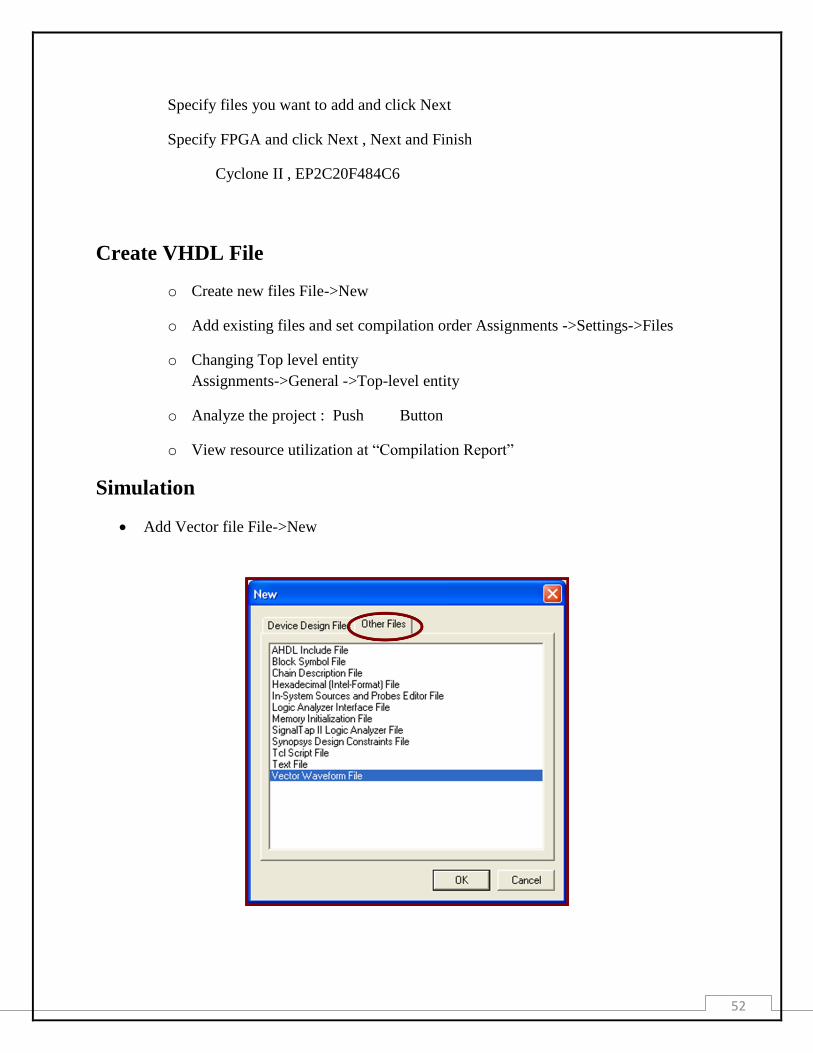
Simulation
Add Vector file File->New
53
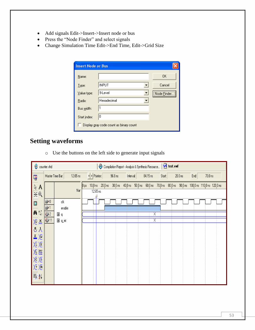
Add signals Edit->Insert->Insert node or bus
Press the “Node Finder” and select signals
Change Simulation Time Edit->End Time, Edit->Grid Size
Setting waveforms
o Use the buttons on the left side to generate input signals
54
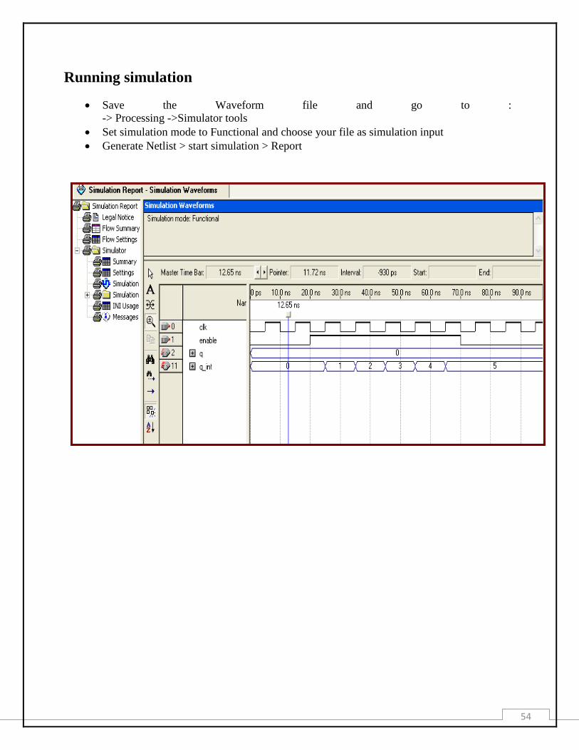
Running simulation
Save the Waveform file and go to :
-> Processing ->Simulator tools
Set simulation mode to Functional and choose your file as simulation input
Generate Netlist > start simulation > Report