Structural, Optical and Electrical Properties of NiO …. Structural Characteristics The x-ray...
4
Structural, Optical and Electrical Properties of NiO Thin Films Prepared by Low Cost Spray Pyrolysis Technique S. Sriram and A. Thayumanavan PG and Research Department of Physics, AVVM Sri Pushpam College (Autonomous), Poondi, Thanjavur, Tamilnadu, India Email: [email protected], [email protected] Abstract—Nickel Oxide (NiO) thin films are fabricated using fresh and aged precursor solutions using a low cost simplified spray pyrolysis technique. Structural, optical and electrical properties of two different films were studied. The structural studies show that the film prepared from the aged solution has more grain size (60.3nm) than the film prepared by fresh solution (21nm). From the optical studies it is found that, the band gap of film from fresh solution have 3.6eV while the band gap of film from aged solution is about 3.5eV. The refractive index (n) is measured with the help of PUMA software and for the film from fresh solution it remains at 1.95 through visible region. However, for the film from aged solution, it varies from 2 to 1.78 in visible region. The calculated extinction coefficient (k) values of the films show no significant variation in visible and NIR range. The electrical studies confirm that the grown films are p- type. The resistivity measured for two films shows that the resistivity is low (2.271×10 2 Ω cm) for the film prepared by fresh solution and it is high (2.725×10 2 Ω cm) for the other one. Index Terms—NiO thin films, perfume atomizer, optical studies, refractive index, electrical studies I. INTRODUCTION Nickel oxide (NiO) is a promising p type semiconducting oxide material [1], [2] having a wide band gap of 3.6eV to 4eV [3]. It resembles NaCl structure with octahedral Ni (II) and (O2-) sites [4]. Due to its enormous potential applications such as, anti- ferromagnetic material [5], [6], chemical sensors [7], electrochromic devices [8], catalysts [9], dye sensitized solar cells (DSSCs) [10], it attracts the researchers attention towards it. NiO thin films were fabricated using many methods such as electron beam evaporation [11], reactive sputtering [12], plasma enhanced chemical vapour deposition [13], pulsed laser deposition [14], spray pyrolysis [15], chemical bath deposition [16] etc. Among various methods, spray pyrolysis is one through which the films can be coated for large area. In this present work a low cost and simplified spray pyrolysis technique using perfume atomizer [17]-[19] is employed Manuscript received September 9, 2013; revised December 30, 2013. to fabricate the NiO thin films. The aging effects of the precursor solution on the optical and electrical properties of the grown films are studied and discussed. II. EXPERIMENTAL DETAIL A set of precursor solution is prepared using Nickel acetate tetrahydrate (Ni (C 2 H 3 O 2 ) 2 .4H 2 O) with 0.1 molarity in ethanol mixed deionized water. One of them is allowed to age about 24 hours and the other one (fresh solution) is taken into use to form NiO film (Sample 1). The second solution (aged solution) is taken after 24 hours and then the second NiO film is fabricated (Sample 2). The volume for both solutions is about 50ml. The substrates used were glasses. The substrates are cleaned in distilled water and then dried using air blower. After that they were cleaned again with acetone in order to remove any strains on it. The solutions were then sprayed manically on the glass substrates with air as carrier gas. The temperature was set to 330ºC. The temperature chosen is due to the acetate in the precursor will decompose above 300ºC. Due to continuous spraying, the substrate temperature is suddenly reduced to 310ºC to 320ºC. Therefore, after every 5 spray, the process was stopped about 5 minutes to recover the substrate temperature to 330ºC. X-ray diffraction analyses were obtained using the model X‟pert PRO (PANalytical) X-ray powder diffractometer with Ni filtered CuKα (1.5406Ǻ) radiation for a range of 10º to 90º 2θ angles. The surface morphology, homogeneity and grain size of the deposited films were studied by SEM model JSM 35 CF JEOL. The optical studies were carried out by Perkin Elmer Lambda 35 UV-VIS-NIR double beam spectrophotometer for a wavelength range of 300nm to 1100nm. Hall effect measurement was carried out with Ecopia HMS 5000 Hall effect measurement system. Thicknesses of the films were measured gravimetrically and the measured thicknesses are 631nm and 676nm for Sample 1 and Sample 2 respectively. III. RESULTS AND DISCUSSION International Journal of Materials Science and Engineering Vol. 1, No. 2 December 2013 ©2013 Engineering and Technology Publishing 118 doi: 10.12720/ijmse.1.2.118-121
-
Upload
trinhquynh -
Category
Documents
-
view
221 -
download
2
Transcript of Structural, Optical and Electrical Properties of NiO …. Structural Characteristics The x-ray...
Structural, Optical and Electrical Properties of
NiO Thin Films Prepared by Low Cost Spray
Pyrolysis Technique
S. Sriram and A. Thayumanavan PG and Research Department of Physics, AVVM Sri Pushpam College (Autonomous), Poondi, Thanjavur, Tamilnadu,
India
Email: [email protected], [email protected]
Abstract—Nickel Oxide (NiO) thin films are fabricated
using fresh and aged precursor solutions using a low cost
simplified spray pyrolysis technique. Structural, optical and
electrical properties of two different films were studied. The
structural studies show that the film prepared from the
aged solution has more grain size (60.3nm) than the film
prepared by fresh solution (21nm). From the optical studies
it is found that, the band gap of film from fresh solution
have 3.6eV while the band gap of film from aged solution is
about 3.5eV. The refractive index (n) is measured with the
help of PUMA software and for the film from fresh solution
it remains at 1.95 through visible region. However, for the
film from aged solution, it varies from 2 to 1.78 in visible
region. The calculated extinction coefficient (k) values of the
films show no significant variation in visible and NIR range.
The electrical studies confirm that the grown films are p-
type. The resistivity measured for two films shows that the
resistivity is low (2.271×10²Ω cm) for the film prepared by
fresh solution and it is high (2.725×10²Ω cm) for the other
one.
Index Terms—NiO thin films, perfume atomizer, optical
studies, refractive index, electrical studies
I. INTRODUCTION
Nickel oxide (NiO) is a promising p type
semiconducting oxide material [1], [2] having a wide
band gap of 3.6eV to 4eV [3]. It resembles NaCl
structure with octahedral Ni (II) and (O2-) sites [4]. Due
to its enormous potential applications such as, anti-
ferromagnetic material [5], [6], chemical sensors [7],
electrochromic devices [8], catalysts [9], dye sensitized
solar cells (DSSCs) [10], it attracts the researchers
attention towards it. NiO thin films were fabricated using
many methods such as electron beam evaporation [11],
reactive sputtering [12], plasma enhanced chemical
vapour deposition [13], pulsed laser deposition [14],
spray pyrolysis [15], chemical bath deposition [16] etc.
Among various methods, spray pyrolysis is one through
which the films can be coated for large area. In this
present work a low cost and simplified spray pyrolysis
technique using perfume atomizer [17]-[19] is employed
Manuscript received September 9, 2013; revised December 30, 2013.
to fabricate the NiO thin films. The aging effects of the
precursor solution on the optical and electrical properties
of the grown films are studied and discussed.
II. EXPERIMENTAL DETAIL
A set of precursor solution is prepared using Nickel
acetate tetrahydrate (Ni (C2H3O2)2.4H2O) with 0.1
molarity in ethanol mixed deionized water. One of them
is allowed to age about 24 hours and the other one (fresh
solution) is taken into use to form NiO film (Sample 1).
The second solution (aged solution) is taken after 24
hours and then the second NiO film is fabricated (Sample
2). The volume for both solutions is about 50ml. The
substrates used were glasses. The substrates are cleaned
in distilled water and then dried using air blower. After
that they were cleaned again with acetone in order to
remove any strains on it. The solutions were then sprayed
manically on the glass substrates with air as carrier gas.
The temperature was set to 330ºC. The temperature
chosen is due to the acetate in the precursor will
decompose above 300ºC. Due to continuous spraying,
the substrate temperature is suddenly reduced to 310ºC to
320ºC. Therefore, after every 5 spray, the process was
stopped about 5 minutes to recover the substrate
temperature to 330ºC.
X-ray diffraction analyses were obtained using the
model X‟pert PRO (PANalytical) X-ray powder
diffractometer with Ni filtered CuKα (1.5406Ǻ) radiation
for a range of 10º to 90º 2θ angles. The surface
morphology, homogeneity and grain size of the deposited
films were studied by SEM model JSM 35 CF JEOL.
The optical studies were carried out by Perkin Elmer
Lambda 35 UV-VIS-NIR double beam
spectrophotometer for a wavelength range of 300nm to
1100nm. Hall effect measurement was carried out with
Ecopia HMS 5000 Hall effect measurement system.
Thicknesses of the films were measured gravimetrically
and the measured thicknesses are 631nm and 676nm for
Sample 1 and Sample 2 respectively.
III. RESULTS AND DISCUSSION
International Journal of Materials Science and Engineering Vol. 1, No. 2 December 2013
©2013 Engineering and Technology Publishing 118doi: 10.12720/ijmse.1.2.118-121
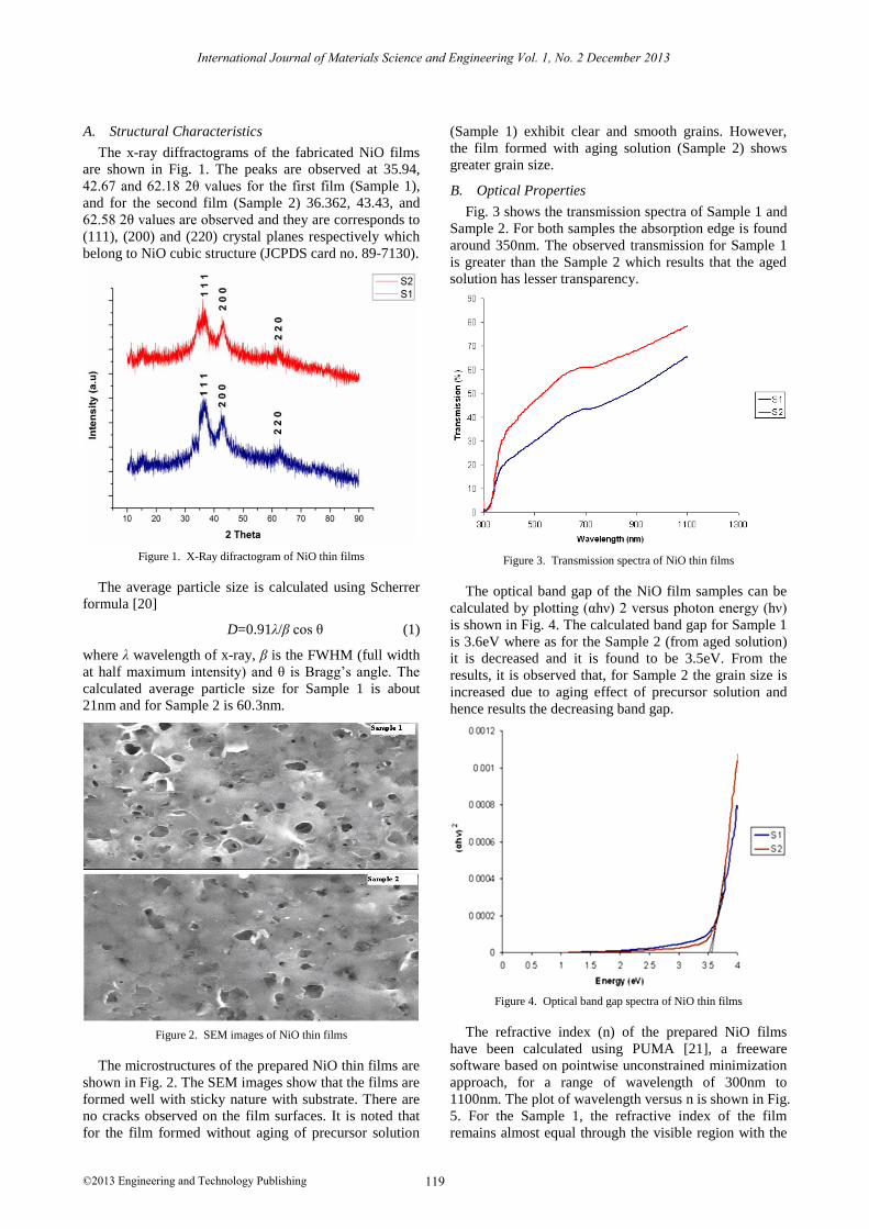
A. Structural Characteristics
The x-ray diffractograms of the fabricated NiO films
are shown in Fig. 1. The peaks are observed at 35.94,
42.67 and 62.18 2θ values for the first film (Sample 1),
and for the second film (Sample 2) 36.362, 43.43, and
62.58 2θ values are observed and they are corresponds to
(111), (200) and (220) crystal planes respectively which
belong to NiO cubic structure (JCPDS card no. 89-7130).
Figure 1. X-Ray difractogram of NiO thin films
The average particle size is calculated using Scherrer
formula [20]
D=0.91λ/β cos θ (1)
where λ wavelength of x-ray, β is the FWHM (full width
at half maximum intensity) and θ is Bragg’s angle. The
calculated average particle size for Sample 1 is about
21nm and for Sample 2 is 60.3nm.
Figure 2. SEM images of NiO thin films
The microstructures of the prepared NiO thin films are
shown in Fig. 2. The SEM images show that the films are
formed well with sticky nature with substrate. There are
no cracks observed on the film surfaces. It is noted that
for the film formed without aging of precursor solution
(Sample 1) exhibit clear and smooth grains. However,
the film formed with aging solution (Sample 2) shows
greater grain size.
B. Optical Properties
Fig. 3 shows the transmission spectra of Sample 1 and
Sample 2. For both samples the absorption edge is found
around 350nm. The observed transmission for Sample 1
is greater than the Sample 2 which results that the aged
solution has lesser transparency.
Figure 3. Transmission spectra of NiO thin films
The optical band gap of the NiO film samples can be
calculated by plotting (αhν) 2 versus photon energy (hν)
is shown in Fig. 4. The calculated band gap for Sample 1
is 3.6eV where as for the Sample 2 (from aged solution)
it is decreased and it is found to be 3.5eV. From the
results, it is observed that, for Sample 2 the grain size is
increased due to aging effect of precursor solution and
hence results the decreasing band gap.
Figure 4. Optical band gap spectra of NiO thin films
The refractive index (n) of the prepared NiO films
have been calculated using PUMA [21], a freeware
software based on pointwise unconstrained minimization
approach, for a range of wavelength of 300nm to
1100nm. The plot of wavelength versus n is shown in Fig.
5. For the Sample 1, the refractive index of the film
remains almost equal through the visible region with the
International Journal of Materials Science and Engineering Vol. 1, No. 2 December 2013
©2013 Engineering and Technology Publishing 119
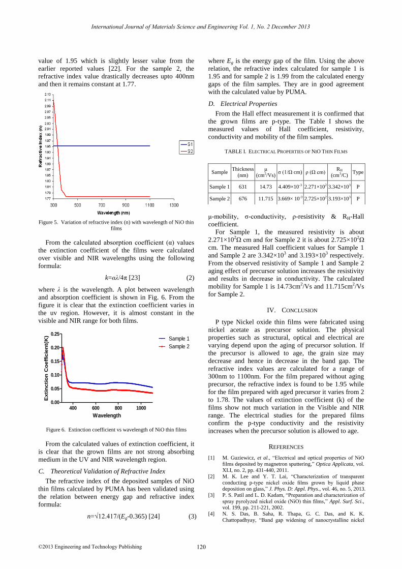
value of 1.95 which is slightly lesser value from the
earlier reported values [22]. For the sample 2, the
refractive index value drastically decreases upto 400nm
and then it remains constant at 1.77.
Figure 5. Variation of refractive index (n) with wavelength of NiO thin films
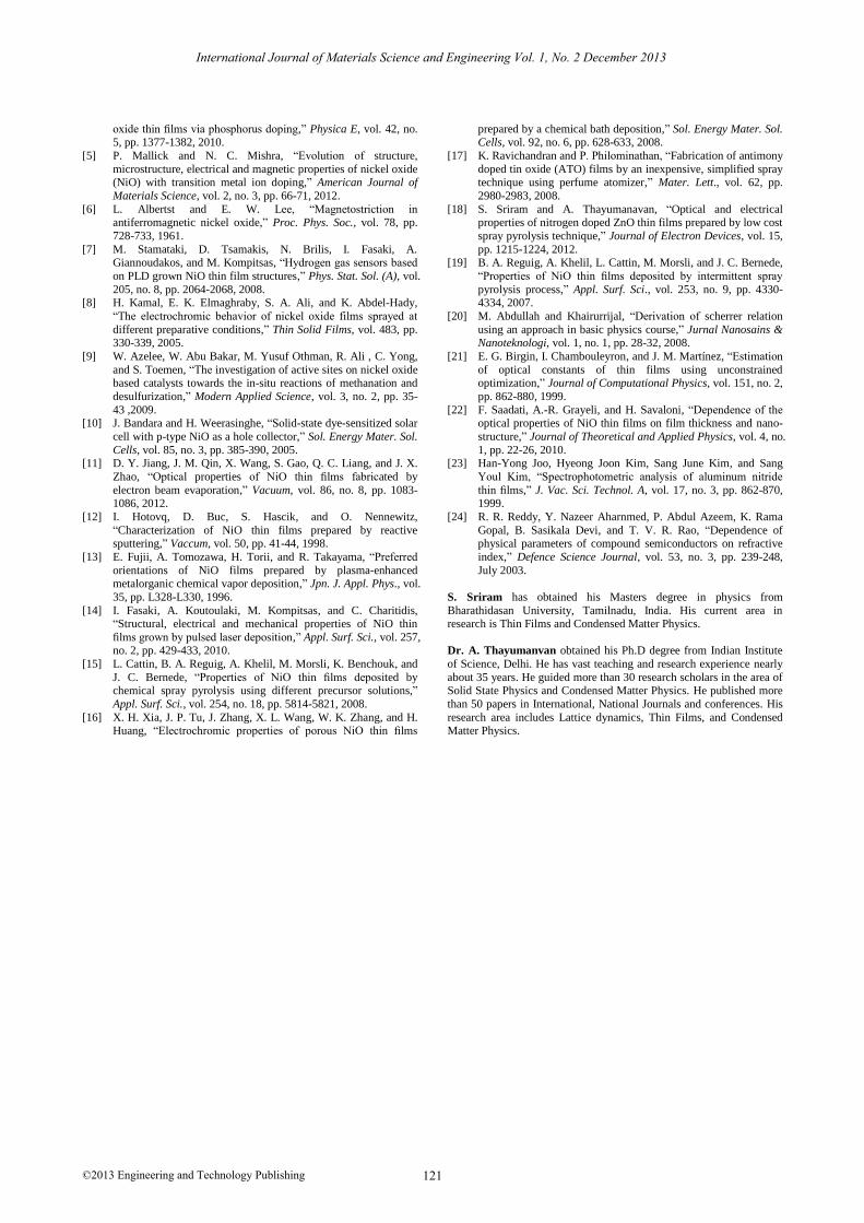
From the calculated absorption coefficient (α) values
the extinction coefficient of the films were calculated
over visible and NIR wavelengths using the following
formula:
k=αλ/4π [23] (2)
where λ is the wavelength. A plot between wavelength
and absorption coefficient is shown in Fig. 6. From the
figure it is clear that the extinction coefficient varies in
the uv region. However, it is almost constant in the
visible and NIR range for both films.
400 600 800 10000.00
0.05
0.10
0.15
0.20
0.25Sample 1
Sample 2
Wavelength
Exti
ncti
on
Co
eff
icie
nt(
K)
Figure 6. Extinction coefficient vs wavelength of NiO thin films
From the calculated values of extinction coefficient, it
is clear that the grown films are not strong absorbing
medium in the UV and NIR wavelength region.
C. Theoretical Validation of Refractive Index
The refractive index of the deposited samples of NiO
thin films calculated by PUMA has been validated using
the relation between energy gap and refractive index
formula:
n=√12.417/(Eg-0.365) [24] (3)
where Eg is the energy gap of the film. Using the above
relation, the refractive index calculated for sample 1 is
1.95 and for sample 2 is 1.99 from the calculated energy
gaps of the film samples. They are in good agreement
with the calculated value by PUMA.
D. Electrical Properties
From the Hall effect measurement it is confirmed that
the grown films are p-type. The Table I shows the
measured values of Hall coefficient, resistivity,
conductivity and mobility of the film samples.
TABLE I. ELECTRICAL PROPERTIES OF NIO THIN FILMS
μ-mobility, σ-conductivity, ρ-resistivity & RH-Hall
coefficient.
For Sample 1, the measured resistivity is about
2.271×10²Ω cm and for Sample 2 it is about 2.725×10
2Ω
cm. The measured Hall coefficient values for Sample 1
and Sample 2 are 3.342×10³ and 3.193×10
3 respectively.
From the observed resistivity of Sample 1 and Sample 2
aging effect of precursor solution increases the resistivity
and results in decrease in conductivity. The calculated
mobility for Sample 1 is 14.73cm2/Vs and 11.715cm
2/Vs
for Sample 2.
IV. CONCLUSION
P type Nickel oxide thin films were fabricated using
nickel acetate as precursor solution. The physical
properties such as structural, optical and electrical are
varying depend upon the aging of precursor solution. If
the precursor is allowed to age, the grain size may
decrease and hence in decrease in the band gap. The
refractive index values are calculated for a range of
300nm to 1100nm. For the film prepared without aging
precursor, the refractive index is found to be 1.95 while
for the film prepared with aged precursor it varies from 2
to 1.78. The values of extinction coefficient (k) of the
films show not much variation in the Visible and NIR
range. The electrical studies for the prepared films
confirm the p-type conductivity and the resistivity
increases when the precursor solution is allowed to age.
REFERENCES
[1] M. Guziewicz, et al., “Electrical and optical properties of NiO
films deposited by magnetron sputtering,” Optica Applicata, vol. XLI, no. 2, pp. 431-440, 2011.
[2] M. K. Lee and Y. T. Lai, “Characterization of transparent
conducting p-type nickel oxide films grown by liquid phase deposition on glass,” J. Phys. D: Appl. Phys., vol. 46, no. 5, 2013.
[3] P. S. Patil and L. D. Kadam, “Preparation and characterization of
spray pyrolyzed nickel oxide (NiO) thin films,” Appl. Surf. Sci., vol. 199, pp. 211-221, 2002.
[4] N. S. Das, B. Saha, R. Thapa, G. C. Das, and K. K.
Chattopadhyay, “Band gap widening of nanocrystalline nickel
Sample Thickness
(nm) μ
(cm2/Vs) σ (1/Ω cm) ρ (Ω cm)
RH (cm3/C)
Type
Sample 1 631 14.73 4.409×10⁻³ 2.271×10² 3.342×10³ P
Sample 2 676 11.715 3.669× 10⁻³ 2.725×10² 3.193×10³ P
International Journal of Materials Science and Engineering Vol. 1, No. 2 December 2013
©2013 Engineering and Technology Publishing 120
oxide thin films via phosphorus doping,” Physica E, vol. 42, no. 5, pp. 1377-1382, 2010.
[5] P. Mallick and N. C. Mishra, “Evolution of structure,
microstructure, electrical and magnetic properties of nickel oxide (NiO) with transition metal ion doping,” American Journal of
Materials Science, vol. 2, no. 3, pp. 66-71, 2012.
[6] L. Albertst and E. W. Lee, “Magnetostriction in antiferromagnetic nickel oxide,” Proc. Phys. Soc., vol. 78, pp.
728-733, 1961.
[7] M. Stamataki, D. Tsamakis, N. Brilis, I. Fasaki, A. Giannoudakos, and M. Kompitsas, “Hydrogen gas sensors based
on PLD grown NiO thin film structures,” Phys. Stat. Sol. (A), vol.
205, no. 8, pp. 2064-2068, 2008. [8] H. Kamal, E. K. Elmaghraby, S. A. Ali, and K. Abdel-Hady,
“The electrochromic behavior of nickel oxide films sprayed at
different preparative conditions,” Thin Solid Films, vol. 483, pp. 330-339, 2005.
[9] W. Azelee, W. Abu Bakar, M. Yusuf Othman, R. Ali , C. Yong,
and S. Toemen, “The investigation of active sites on nickel oxide based catalysts towards the in-situ reactions of methanation and
desulfurization,” Modern Applied Science, vol. 3, no. 2, pp. 35-
43 ,2009. [10] J. Bandara and H. Weerasinghe, “Solid-state dye-sensitized solar
cell with p-type NiO as a hole collector,” Sol. Energy Mater. Sol.
Cells, vol. 85, no. 3, pp. 385-390, 2005. [11] D. Y. Jiang, J. M. Qin, X. Wang, S. Gao, Q. C. Liang, and J. X.
Zhao, “Optical properties of NiO thin films fabricated by
electron beam evaporation,” Vacuum, vol. 86, no. 8, pp. 1083-1086, 2012.
[12] I. Hotovq, D. Buc, S. Hascik, and O. Nennewitz,
“Characterization of NiO thin films prepared by reactive sputtering,” Vaccum, vol. 50, pp. 41-44, 1998.
[13] E. Fujii, A. Tomozawa, H. Torii, and R. Takayama, “Preferred
orientations of NiO films prepared by plasma-enhanced metalorganic chemical vapor deposition,” Jpn. J. Appl. Phys., vol.
35, pp. L328-L330, 1996.
[14] I. Fasaki, A. Koutoulaki, M. Kompitsas, and C. Charitidis, “Structural, electrical and mechanical properties of NiO thin
films grown by pulsed laser deposition,” Appl. Surf. Sci., vol. 257, no. 2, pp. 429-433, 2010.
[15] L. Cattin, B. A. Reguig, A. Khelil, M. Morsli, K. Benchouk, and
J. C. Bernede, “Properties of NiO thin films deposited by chemical spray pyrolysis using different precursor solutions,”
Appl. Surf. Sci., vol. 254, no. 18, pp. 5814-5821, 2008.
[16] X. H. Xia, J. P. Tu, J. Zhang, X. L. Wang, W. K. Zhang, and H. Huang, “Electrochromic properties of porous NiO thin films
prepared by a chemical bath deposition,” Sol. Energy Mater. Sol. Cells, vol. 92, no. 6, pp. 628-633, 2008.
[17] K. Ravichandran and P. Philominathan, “Fabrication of antimony
doped tin oxide (ATO) films by an inexpensive, simplified spray technique using perfume atomizer,” Mater. Lett., vol. 62, pp.
2980-2983, 2008.
[18] S. Sriram and A. Thayumanavan, “Optical and electrical properties of nitrogen doped ZnO thin films prepared by low cost
spray pyrolysis technique,” Journal of Electron Devices, vol. 15,
pp. 1215-1224, 2012. [19] B. A. Reguig, A. Khelil, L. Cattin, M. Morsli, and J. C. Bernede,
“Properties of NiO thin films deposited by intermittent spray
pyrolysis process,” Appl. Surf. Sci., vol. 253, no. 9, pp. 4330-4334, 2007.
[20] M. Abdullah and Khairurrijal, “Derivation of scherrer relation
using an approach in basic physics course,” Jurnal Nanosains & Nanoteknologi, vol. 1, no. 1, pp. 28-32, 2008.
[21] E. G. Birgin, I. Chambouleyron, and J. M. Martínez, “Estimation
of optical constants of thin films using unconstrained optimization,” Journal of Computational Physics, vol. 151, no. 2,
pp. 862-880, 1999.
[22] F. Saadati, A.-R. Grayeli, and H. Savaloni, “Dependence of the optical properties of NiO thin films on film thickness and nano-
structure,” Journal of Theoretical and Applied Physics, vol. 4, no.
1, pp. 22-26, 2010. [23] Han-Yong Joo, Hyeong Joon Kim, Sang June Kim, and Sang
Youl Kim, “Spectrophotometric analysis of aluminum nitride
thin films,” J. Vac. Sci. Technol. A, vol. 17, no. 3, pp. 862-870, 1999.
[24] R. R. Reddy, Y. Nazeer Aharnmed, P. Abdul Azeem, K. Rama
Gopal, B. Sasikala Devi, and T. V. R. Rao, “Dependence of physical parameters of compound semiconductors on refractive
index,” Defence Science Journal, vol. 53, no. 3, pp. 239-248,
July 2003.
S. Sriram has obtained his Masters degree in physics from
Bharathidasan University, Tamilnadu, India. His current area in research is Thin Films and Condensed Matter Physics.
Dr. A. Thayumanvan obtained his Ph.D degree from Indian Institute
of Science, Delhi. He has vast teaching and research experience nearly
about 35 years. He guided more than 30 research scholars in the area of Solid State Physics and Condensed Matter Physics. He published more
than 50 papers in International, National Journals and conferences. His
research area includes Lattice dynamics, Thin Films, and Condensed Matter Physics.
International Journal of Materials Science and Engineering Vol. 1, No. 2 December 2013
©2013 Engineering and Technology Publishing 121