PA09 • PA09A - Apex Microtechnology - Power … · 1 1 3 10 30 100 1k300 } ... log.com for Apex...
15
www.apexanalog.com © Apex Microtechnology Inc. All rights reserved Apr 2018 PA09U Rev S Power Operational Amplifier RoHS COMPLIANT PA09 • PA09A FEATURES • Power MOS Technology — 5A Peak Rating • High Gain Bandwidth Product — 150 MHz • Very Fast Slew Rate — 200V/μs • Protected Output Stage — Thermal Shutoff • Excellent Linearity — Class A/B Output • Wide Supply Range — ±12V To ±40V • Low Bias Current, Low Noise — FET Input APPLICATIONS • Video Distribution and Amplification • High Speed Deflection Circuits • Power Transducers To 2 MHz • Coaxial Line Drivers • Power LED Or Laser Diode Excitation DESCRIPTION The PA09 is a high voltage, high output current operational amplifier optimized to drive a variety of loads from DC through the video frequency range. Excellent input accuracy is achieved with a dual monolithic FET input transistor which is cascoded by two high voltage transistors to provide outstanding common mode characteristics. All internal current and voltage levels are referenced to a zener diode biased on by a current source. As a result, the PA09 exhibits superior DC and AC stability over a wide supply and temperature range. High speed and freedom from second breakdown is assured by a complementary Power MOS output stage. For optimum linearity, especially at low levels, the Power MOS transistors are biased in the class A/B mode. Thermal shutoff provides full protection against overheating and limits the heatsink requirements to dissipate the internal power losses under normal operating conditions. A built-in current limit protects the amplifier against overloading. Transient inductive load kickback protection is provided by two internal clamp- ing diodes. External phase compensation allows the user maximum flexibility in obtaining the optimum slew rate and gain bandwidth product at all gain settings. For continuous operation under load, a heatsink of proper rating is recommended. This hybrid integrated circuit utilizes thick film (cermet) resistors, ceramic capacitors and silicon semicon- ductor chips to maximize reliability, minimize size and give top performance. Ultrasonically bonded alumi- num wires provide reliable interconnections at all operating temperatures. The CE, 8-pin TO-3 package is hermetically sealed and electrically isolated. The use of compressible thermal washers and/or improper mounting torque will void the product warranty. Please see Applications Note 1 “General Operating Condi- tions.”
Transcript of PA09 • PA09A - Apex Microtechnology - Power … · 1 1 3 10 30 100 1k300 } ... log.com for Apex...
www.apexanalog.com© Apex Microtechnology Inc
All rights reserved
Power Operational Am
PA09 • PA09A
plifier RoHSCOMPLIANT
FEATURES
• Power MOS Technology — 5A Peak Rating• High Gain Bandwidth Product — 150 MHz• Very Fast Slew Rate — 200V/μs• Protected Output Stage — Thermal Shutoff• Excellent Linearity — Class A/B Output• Wide Supply Range — ±12V To ±40V• Low Bias Current, Low Noise — FET Input
APPLICATIONS
• Video Distribution and Amplification• High Speed Deflection Circuits• Power Transducers To 2 MHz• Coaxial Line Drivers• Power LED Or Laser Diode Excitation
DESCRIPTION
The PA09 is a high voltage, high output current operational amplifier optimized to drive a variety of loadsfrom DC through the video frequency range. Excellent input accuracy is achieved with a dual monolithic FETinput transistor which is cascoded by two high voltage transistors to provide outstanding common modecharacteristics. All internal current and voltage levels are referenced to a zener diode biased on by a currentsource. As a result, the PA09 exhibits superior DC and AC stability over a wide supply and temperature range.
High speed and freedom from second breakdown is assured by a complementary Power MOS outputstage. For optimum linearity, especially at low levels, the Power MOS transistors are biased in the class A/Bmode. Thermal shutoff provides full protection against overheating and limits the heatsink requirements todissipate the internal power losses under normal operating conditions. A built-in current limit protects theamplifier against overloading. Transient inductive load kickback protection is provided by two internal clamp-ing diodes. External phase compensation allows the user maximum flexibility in obtaining the optimum slewrate and gain bandwidth product at all gain settings. For continuous operation under load, a heatsink ofproper rating is recommended.
This hybrid integrated circuit utilizes thick film (cermet) resistors, ceramic capacitors and silicon semicon-ductor chips to maximize reliability, minimize size and give top performance. Ultrasonically bonded alumi-num wires provide reliable interconnections at all operating temperatures. The CE, 8-pin TO-3 package ishermetically sealed and electrically isolated. The use of compressible thermal washers and/or impropermounting torque will void the product warranty. Please see Applications Note 1 “General Operating Condi-tions.”
. Apr 2018PA09U Rev S
PA09 • PA09A
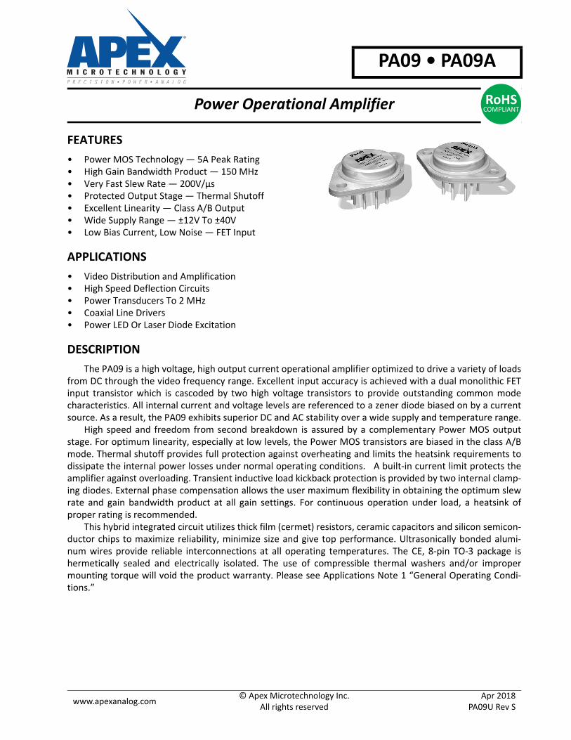
TYPICAL CONNECTION
Figure 1: Typical Connection
2 PA09U Rev S
PA09 • PA09A
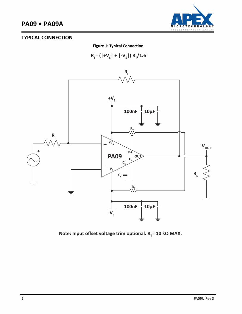
PINOUT AND DESCRIPTION TABLE
Figure 2: External Connections
Pin Number Name Description
1 OUT The output. Connect this pin to load and to the feedback resistors.
2 BAL Balance Control pin. Adjusts voltage offset. See applicable section.
3 +Vs The positive supply rail.
4 +IN The non-inverting input.
5 -IN The inverting input.
6 -Vs The negative supply rail.
7 RCCompensation resistor connection. Select value based on Phase Compensation.
See applicable section.
8 CCCompensation capacitor connection. Select value based on Phase Compensation.
See applicable section.
PA09U Rev S 3
PA09 • PA09A
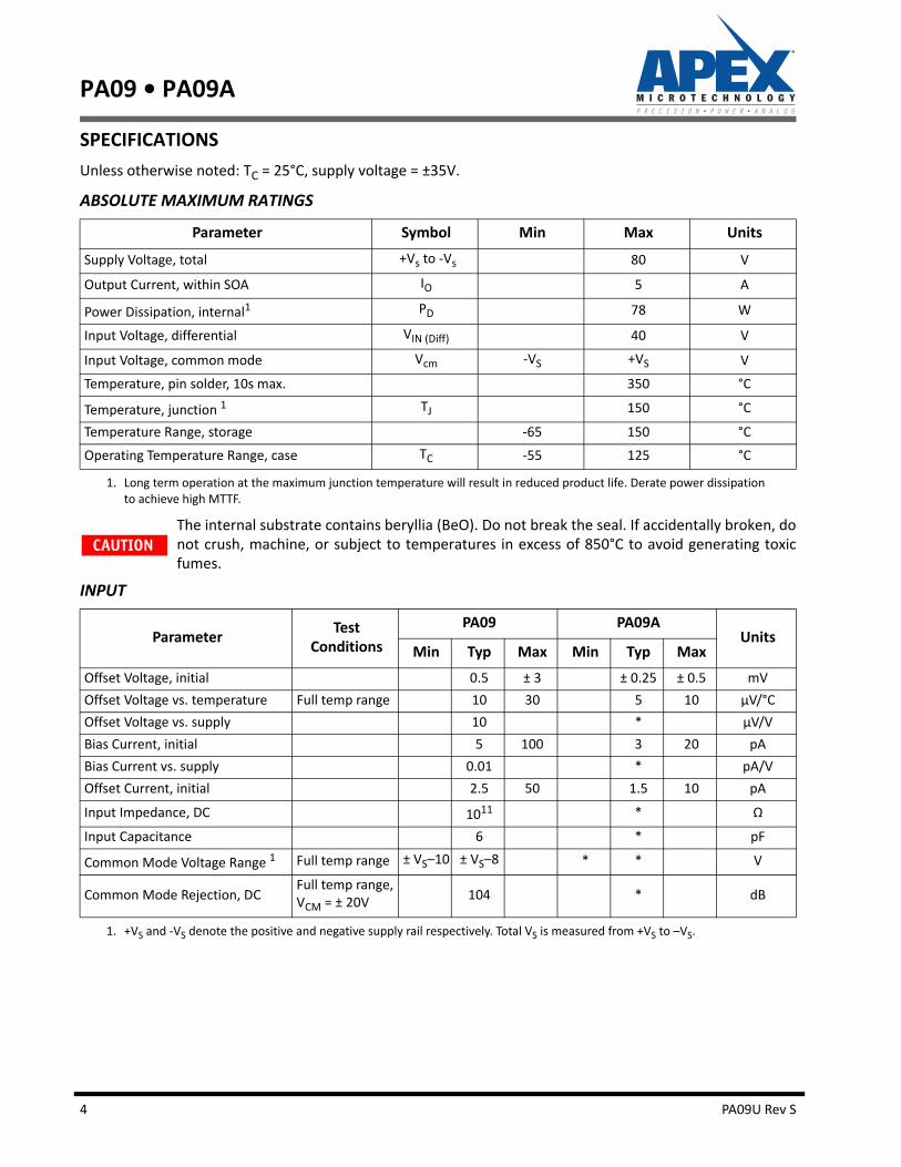
SPECIFICATIONS
Unless otherwise noted: TC = 25°C, supply voltage = ±35V.
ABSOLUTE MAXIMUM RATINGS
The internal substrate contains beryllia (BeO). Do not break the seal. If accidentally broken, donot crush, machine, or subject to temperatures in excess of 850°C to avoid generating toxicfumes.
INPUT
Parameter Symbol Min Max Units
Supply Voltage, total +Vs to -Vs 80 V
Output Current, within SOA IO 5 A
Power Dissipation, internal1
1. Long term operation at the maximum junction temperature will result in reduced product life. Derate power dissipation to achieve high MTTF.
PD 78 W
Input Voltage, differential VIN (Diff) 40 V
Input Voltage, common mode Vcm -VS +VS V
Temperature, pin solder, 10s max. 350 °C
Temperature, junction 1 TJ 150 °C
Temperature Range, storage -65 150 °C
Operating Temperature Range, case TC -55 125 °C
ParameterTest
Conditions
PA09 PA09AUnits
Min Typ Max Min Typ Max
Offset Voltage, initial 0.5 ± 3 ± 0.25 ± 0.5 mV
Offset Voltage vs. temperature Full temp range 10 30 5 10 µV/°C
Offset Voltage vs. supply 10 * µV/V
Bias Current, initial 5 100 3 20 pA
Bias Current vs. supply 0.01 * pA/V
Offset Current, initial 2.5 50 1.5 10 pA
Input Impedance, DC 1011 * Ω
Input Capacitance 6 * pF
Common Mode Voltage Range 1
1. +VS and -VS denote the positive and negative supply rail respectively. Total VS is measured from +VS to –VS.
Full temp range ± VS–10 ± VS–8 * * V
Common Mode Rejection, DCFull temp range, VCM = ± 20V
104 * dB
CAUTION
4 PA09U Rev S
PA09 • PA09A
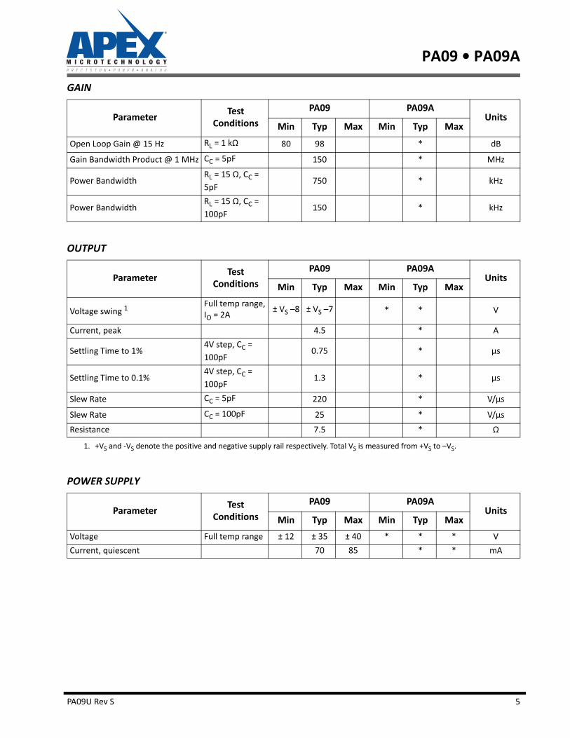
GAIN
OUTPUT
POWER SUPPLY
ParameterTest
Conditions
PA09 PA09AUnits
Min Typ Max Min Typ Max
Open Loop Gain @ 15 Hz RL = 1 kΩ 80 98 * dB
Gain Bandwidth Product @ 1 MHz CC = 5pF 150 * MHz
Power BandwidthRL = 15 Ω, CC =
5pF750 * kHz
Power BandwidthRL = 15 Ω, CC =
100pF150 * kHz
ParameterTest
Conditions
PA09 PA09AUnits
Min Typ Max Min Typ Max
Voltage swing 1
1. +VS and -VS denote the positive and negative supply rail respectively. Total VS is measured from +VS to –VS.
Full temp range, IO = 2A
± VS –8 ± VS –7 * * V
Current, peak 4.5 * A
Settling Time to 1%4V step, CC =
100pF0.75 * µs
Settling Time to 0.1%4V step, CC =
100pF1.3 * µs
Slew Rate CC = 5pF 220 * V/µs
Slew Rate CC = 100pF 25 * V/µs
Resistance 7.5 * Ω
ParameterTest
Conditions
PA09 PA09AUnits
Min Typ Max Min Typ Max
Voltage Full temp range ± 12 ± 35 ± 40 * * * V
Current, quiescent 70 85 * * mA
PA09U Rev S 5
PA09 • PA09A
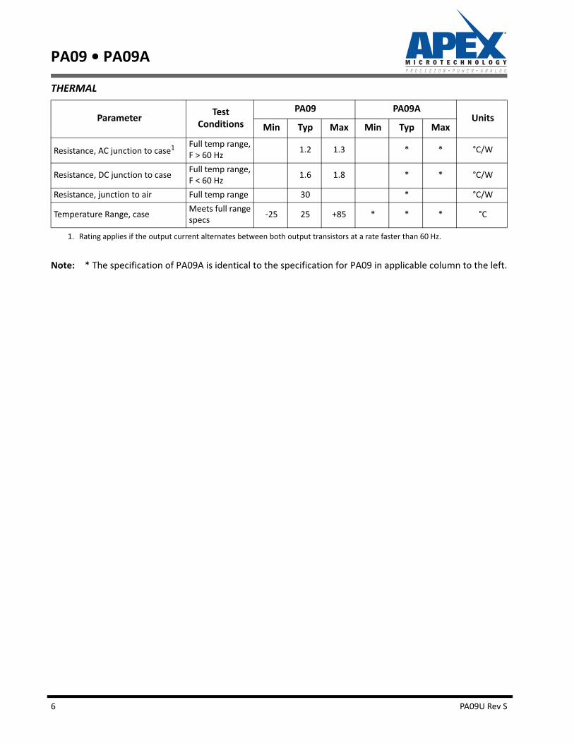
THERMAL
Note: * The specification of PA09A is identical to the specification for PA09 in applicable column to the left.
ParameterTest
Conditions
PA09 PA09AUnits
Min Typ Max Min Typ Max
Resistance, AC junction to case1
1. Rating applies if the output current alternates between both output transistors at a rate faster than 60 Hz.
Full temp range, F > 60 Hz
1.2 1.3 * * °C/W
Resistance, DC junction to caseFull temp range, F < 60 Hz
1.6 1.8 * * °C/W
Resistance, junction to air Full temp range 30 * °C/W
Temperature Range, caseMeets full range specs
-25 25 +85 * * * °C
6 PA09U Rev S
PA09 • PA09A
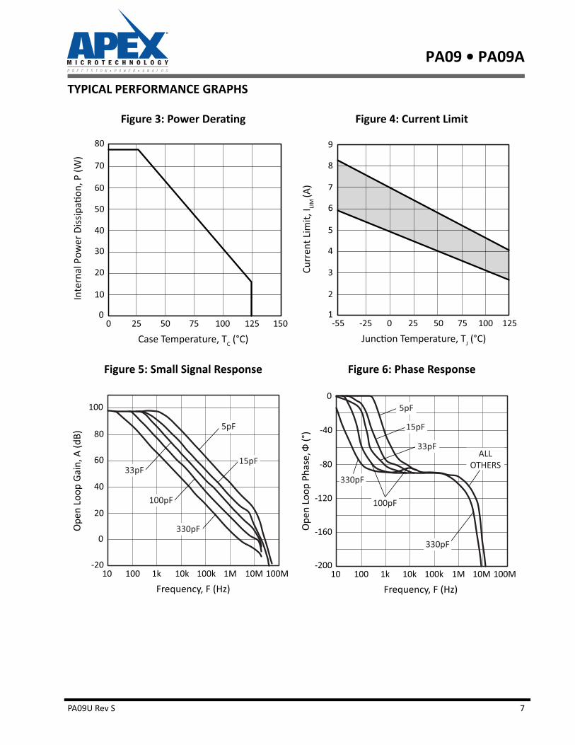
TYPICAL PERFORMANCE GRAPHS
Figure 3: Power Derating Figure 4: Current Limit
Figure 5: Small Signal Response Figure 6: Phase Response
80
70
60
50
40
30
20
10
00 25 50 75 100 150125
Case Temperature, TC (°C)
9
8
7
6
5
4
3
2
1-55 -25 25 50 75 125100
J °C)
)0
100
80
60
40
20
0
-2010 100 1k 10k 100k 10M
Frequency, F (Hz)
Ope
n Lo
op G
ain,
A (d
B)
1M
5pF
33pF
100pF
15pF
330pF
100M
0
-40
-80
-120
-160
-20010 100 1k 10k 1M 100M10M
Frequency, F (Hz)
Ope
n Lo
op P
hase
, )
100k
5pF
33pF
330pF
100pF
15pF
ALLOTHERS
330pF
PA09U Rev S 7
PA09 • PA09A
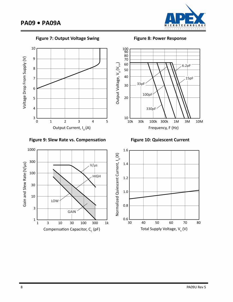
Figure 7: Output Voltage Swing Figure 8: Power Response
Figure 9: Slew Rate vs. Compensation Figure 10: Quiescent Current
10
9
8
7
6
5
4
30 1 2 3 54
Output Current, IO (A)
Volta
ge D
rop
From
Sup
ply
(V)
1009080706050
40
20
1010k 30k 100k 300k 1M 10M3M
Frequency, F (Hz)
Out
put V
olta
ge, V
O (V
P-P)
30
6.2pF
33pF
100pF
330pF
15pF
1000
300
100
30
10
3
11 3 10 30 100 1k300
C )
V/μs
)
HIGH
V/μs
GAIN
LOW
1.6
1.4
1.2
1.0
0.8
0.630 40 50 60 8070
Total Supply Voltage, VS (V)
Nor
mal
ized
Qui
esce
nt C
urre
nt, I
Q (X
)
8 PA09U Rev S
PA09 • PA09A
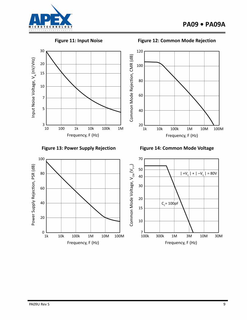
Figure 11: Input Noise Figure 12: Common Mode Rejection
Figure 13: Power Supply Rejection Figure 14: Common Mode Voltage
30
20
15
10
7
5
310 100 1k 10k 1M100k
Frequency, F (Hz)
Inpu
t Noi
se V
olta
ge, V
N (
)
120
100
80
60
40
201k 10k 100k 1M 100M10M
Frequency, F (Hz))
20
100
80
60
40
01k 10k 100k 1M 100M10M
Frequency, F (Hz)
)
70
50
40
30
20
15
10
7100k 300k 1M 3M 30M10M
Frequency, F (Hz)
Com
mon
Mod
e Vo
ltage
, VCM
(VP-
P)
| +VS | + | –VS | = 80V
CC= 100pF
PA09U Rev S 9
PA09 • PA09A
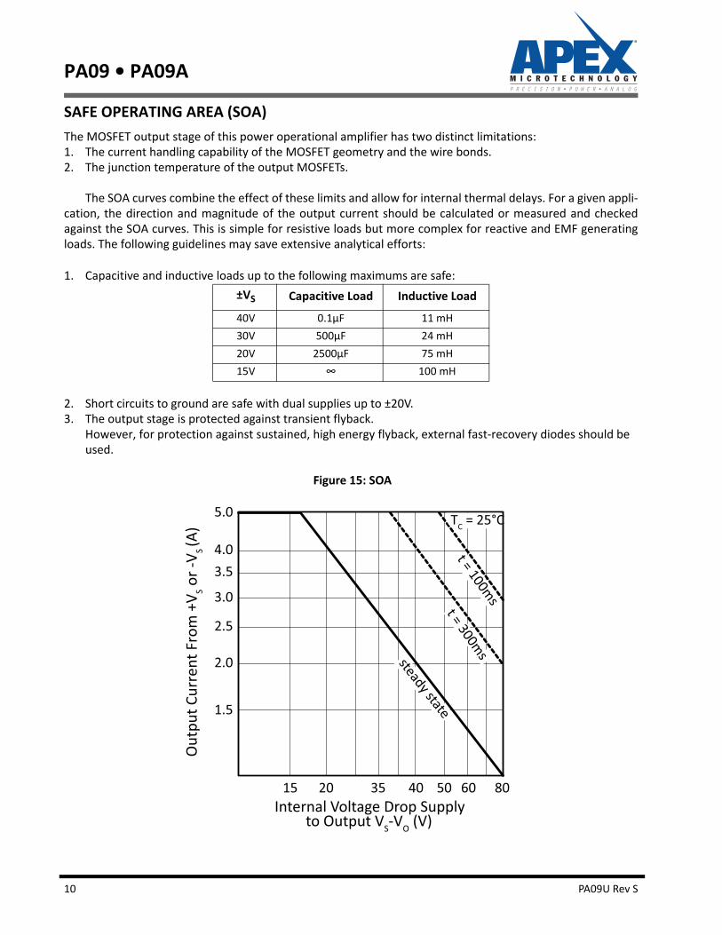
SAFE OPERATING AREA (SOA)
The MOSFET output stage of this power operational amplifier has two distinct limitations:1. The current handling capability of the MOSFET geometry and the wire bonds.2. The junction temperature of the output MOSFETs.
The SOA curves combine the effect of these limits and allow for internal thermal delays. For a given appli-cation, the direction and magnitude of the output current should be calculated or measured and checkedagainst the SOA curves. This is simple for resistive loads but more complex for reactive and EMF generatingloads. The following guidelines may save extensive analytical efforts:
1. Capacitive and inductive loads up to the following maximums are safe:
2. Short circuits to ground are safe with dual supplies up to ±20V.3. The output stage is protected against transient flyback.
However, for protection against sustained, high energy flyback, external fast-recovery diodes should beused.
Figure 15: SOA
±VS Capacitive Load Inductive Load
40V 0.1µF 11 mH
30V 500µF 24 mH
20V 2500µF 75 mH
15V ∞ 100 mH
5.0
4.03.5
2.5
2.0
1.5
15 20 40 50 8060Internal Voltage Drop Supply
Out
put C
urre
nt F
rom
+V S o
r -V S
(A)
to Output VS-VO (V)
TC = 25°C
t = 100ms
steady statet = 300m
s
35
3.0
10 PA09U Rev S
PA09 • PA09A
GENERAL
Please read Application Note 1 “General Operating Considerations” which covers stability, supplies, heatsinking, mounting, current limit, SOA interpretation, and specification interpretation. Visit www.apexana-log.com for Apex Microtechnology's complete Application Notes library, Technical Seminar Workbook, andEvaluation Kits.
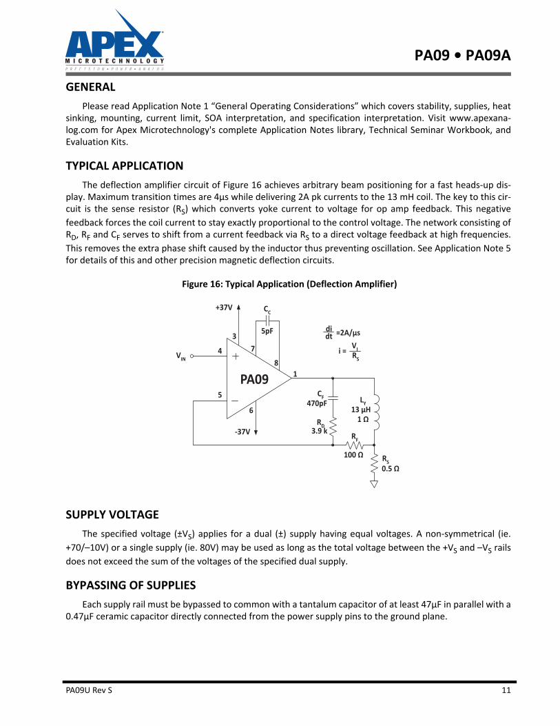
TYPICAL APPLICATION
The deflection amplifier circuit of Figure 16 achieves arbitrary beam positioning for a fast heads-up dis-play. Maximum transition times are 4µs while delivering 2A pk currents to the 13 mH coil. The key to this cir-cuit is the sense resistor (RS) which converts yoke current to voltage for op amp feedback. This negative
feedback forces the coil current to stay exactly proportional to the control voltage. The network consisting ofRD, RF and CF serves to shift from a current feedback via RS to a direct voltage feedback at high frequencies.
This removes the extra phase shift caused by the inductor thus preventing oscillation. See Application Note 5for details of this and other precision magnetic deflection circuits.
Figure 16: Typical Application (Deflection Amplifier)
SUPPLY VOLTAGE
The specified voltage (±VS) applies for a dual (±) supply having equal voltages. A non-symmetrical (ie.
+70/–10V) or a single supply (ie. 80V) may be used as long as the total voltage between the +VS and –VS rails
does not exceed the sum of the voltages of the specified dual supply.
BYPASSING OF SUPPLIES
Each supply rail must be bypassed to common with a tantalum capacitor of at least 47µF in parallel with a0.47µF ceramic capacitor directly connected from the power supply pins to the ground plane.
PA09U Rev S 11
PA09 • PA09A
OUTPUT LEADS
Keep the output leads as short as possible. In the video frequency range, even a few inches of wire havesignificant inductance, raising the interconnection impedance and limiting the output current slew rate. Fur-thermore, the skin effect increases the resistance of heavy wires at high frequencies. Multistrand Litz Wire isrecommended to carry large video currents with low losses.
GROUNDING
Single point grounding of the input resistors and the input signal to a common ground plane will preventundesired current feedback, which can cause large errors and/ or instabilities. “Single point” is a key phrasehere; a ground plane should be used as shielding rather than a current path. Leaving the case of the PA09floating will cause oscillations in some applications.
COMPENSATION
The PA09 is extremely flexible in terms of choice of compensation capacitor for any given gain. The mostcommon ranges are shown in the Small Signal Response graph. Swinging closer to the supply rails, heavierloads, faster input signal rise and fall times and higher supply voltages all tend to demand larger values ofcompensation capacitor. This capacitor must be rated at least as high as the total voltage applied to theamplifier. In making specific value choices, use the square wave stability test presented in APPLICATION NOTE19, Figures 40 and 41.
In addition to small signal testing, if the application includes step functions in the input signal, use this cir-cuit to measure large signal response. By increasing square wave amplitude to the maximum of the applica-tion, this test may show significant distortion of the output waveform following the square wave transitions.In this case the faster input stages of the PA09 are out-running the output stage and overload recovery timecreates the distortion. This speed relationship is also why slew rate does not increase for compensation val-ues below about 27pF.
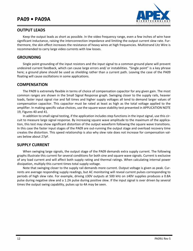
SUPPLY CURRENT
When swinging large signals, the output stage of the PA09 demands extra supply current. The followinggraphs illustrate this current for several conditions for both sine and square wave signals. Current is exclusiveof any load current and will affect both supply rating and thermal ratings. When calculating internal powerdissipation, multiply this current times total supply voltage.
Note that swinging closer to the supply rail demands more current. Output voltage is given as peak. Cur-rents are average responding supply readings, but AC monitoring will reveal current pulses corresponding toperiods of high slew rate. For example, driving ±30V outputs at 500 kHz on ±40V supplies produces a 0.8Apulse during negative slew and a 1.2A pulse during positive slew. If the input signal is over driven by severaltimes the output swing capability, pulses up to 4A may be seen.
12 PA09U Rev S
PA09 • PA09A
Figure 17: Quiescent vs. Sine Drive
Figure 18: Quiescent vs. Square Drive
THERMAL SHUTDOWN PROTECTION
The thermal protection circuit shuts off the amplifier when the substrate temperature exceeds approxi-mately 150°C. This allows heatsink selection to be based on normal operating conditions while protecting theamplifier against excessive junction temperature during temporary fault conditions.
Thermal protection is a fairly slow-acting circuit and therefore does not protect the amplifier againsttransient SOA violations (areas outside of the TC = 25°C boundary). It is designed to protect against short-
term fault conditions that result in high power dissipation within the amplifier, If the conditions that causethermal shutdown are not removed, the amplifier will oscillate in and out of shutdown. This will result in highpeak power stresses, destroy signal integrity, and reduce the reliability of the device.
1.5
1.4
1.3
1.2
1.1
1.0100k 300k 1M
Frequency, F (Hz)
Nor
mal
ized
I Q (X
)
15V O
/23V
S
32V O
/40V
S
15V O /4
0VS
7.0
5.5
4.0
2.5
1.010k 100k 1M
Frequency, F (Hz)
Nor
mal
ized
I Q (X
)
32VO /40VS
15VO /23VS
15VO /40VS
PA09U Rev S 13
PA09 • PA09A
STABILITY
Due to its large bandwidth the PA09 is more likely to oscillate than lower bandwidth Power OperationalAmplifiers. To prevent oscillations a reasonable phase margin must be maintained by:1. Pay very careful attention to supply bypassing and circuit grounding. This is very important when step
functions are driven and the PA09 shares supplies with more active devices.2. Keeping the external sumpoint stray capacitance to ground at a minimum and the sumpoint load resis-
tance (input and feedback resistors in parallel) below 500 Ω. Larger sumpoint load resistances can be used with increased phase compensation and/ or bypassing of the feedback resistor.
3. Connect the case to a local AC ground potential.
CURRENT LIMIT
Internal current limiting is provided in the PA09. Note the current limit curve given under typical perfor-mance graphs is based on junction temperature. If the amplifier is operated at cold junction temperatures,current limit could be as high as 8A. This is above the maximum allowed current on the SOA curve of 5A. Sys-tems using this part must be designed to keep the maximum output current to less than 5 amps under allconditions. The internal current limit only provides this protection for junction temperatures of 80°C andabove.
14 PA09U Rev S
PA09 • PA09A
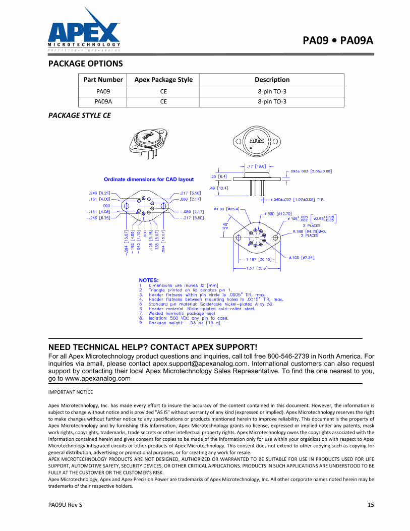
PACKAGE OPTIONS
PACKAGE STYLE CE
Part Number Apex Package Style Description
PA09 CE 8-pin TO-3
PA09A CE 8-pin TO-3
PA09U Rev S 15
NEED TECHNICAL HELP? CONTACT APEX SUPPORT! For all Apex Microtechnology product questions and inquiries, call toll free 800-546-2739 in North America. Forinquiries via email, please contact [email protected]. International customers can also requestsupport by contacting their local Apex Microtechnology Sales Representative. To find the one nearest to you,go to www.apexanalog.com
IMPORTANT NOTICE
Apex Microtechnology, Inc. has made every effort to insure the accuracy of the content contained in this document. However, the information is
subject to change without notice and is provided "AS IS" without warranty of any kind (expressed or implied). Apex Microtechnology reserves the right
to make changes without further notice to any specifications or products mentioned herein to improve reliability. This document is the property ofApex Microtechnology and by furnishing this information, Apex Microtechnology grants no license, expressed or implied under any patents, mask
work rights, copyrights, trademarks, trade secrets or other intellectual property rights. Apex Microtechnology owns the copyrights associated with the
information contained herein and gives consent for copies to be made of the information only for use within your organization with respect to ApexMicrotechnology integrated circuits or other products of Apex Microtechnology. This consent does not extend to other copying such as copying for
general distribution, advertising or promotional purposes, or for creating any work for resale.
APEX MICROTECHNOLOGY PRODUCTS ARE NOT DESIGNED, AUTHORIZED OR WARRANTED TO BE SUITABLE FOR USE IN PRODUCTS USED FOR LIFESUPPORT, AUTOMOTIVE SAFETY, SECURITY DEVICES, OR OTHER CRITICAL APPLICATIONS. PRODUCTS IN SUCH APPLICATIONS ARE UNDERSTOOD TO BE
FULLY AT THE CUSTOMER OR THE CUSTOMER’S RISK.
Apex Microtechnology, Apex and Apex Precision Power are trademarks of Apex Microtechnology, Inc. All other corporate names noted herein may betrademarks of their respective holders.