The Surface Mechanomyogram (MMG) 3.44 ms -2 1.82 Volts 55 Nm seconds 0312 406 μV.
Upload
duongthuanCategory
view
214download
0
50 n
V/d
iv
Time (1 s/div)
Product
Folder
Order
Now
Technical
Documents
Tools &
Software
Support &Community
ReferenceDesign
An IMPORTANT NOTICE at the end of this data sheet addresses availability, warranty, changes, use in safety-critical applications,intellectual property matters and other important disclaimers. PRODUCTION DATA.
OPA180, OPA2180, OPA4180SBOS584E –NOVEMBER 2011–REVISED JUNE 2018
OPAx180 0.1-μV/°C Drift, Low-Noise, Rail-to-Rail Output, 36-V,Zero-Drift Operational Amplifiers
1
1 Features1• Low Offset Voltage: 75 μV (Maximum)• Zero-Drift: 0.1 μV/°C• Low Noise: 10 nV/√Hz• Very Low 1/f Noise• Excellent DC Precision:
– PSRR: 126 dB– CMRR: 114 dB– Open-Loop Gain (AOL): 120 dB
• Quiescent Current: 525 μA (Maximum)• Wide Supply Range: ±2 V to ±18 V• Rail-to-Rail Output:
Input Includes Negative Rail• Low Bias Current: 250 pA (Typical)• RFI Filtered Inputs• MicroSIZE Packages
2 Applications• Bridge Amplifiers• Strain Gauges• Test Equipment• Transducer Applications• Temperature Measurement• Electronic Scales• Medical Instrumentation• Resister Thermal Detectors• Precision Active Filters
3 DescriptionThe OPA180, OPA2180 and OPA4180 operationalamplifiers (op amps) use TI's proprietary zero-drifttechniques to simultaneously provide low offsetvoltage (75 μV), and near zero-drift over time andtemperature. These miniature, high-precision, low-quiescent-current op amps offer high inputimpedance and rail-to-rail output swing within 18 mVof the rails. The input common-mode range includesthe negative rail. Single- or dual-supplies rangingfrom 4 V to 36 V (±2 V to ±18 V) can be used.
The dual-channel version is offered in VSSOP-8packages and SOIC-8 packages. The quad-channelversion is offered in SOIC-14 and TSSOP-14packages. The single and quad package offerings(OPA180 and OPA4180) are specified from –40°C to+125°C, and the dual package (OPA2180) isspecified from –40°C to +105°C.
Device Information(1)
DEVICE NAME PACKAGE BODY SIZE (NOM)
OPA180SOT-23 (5) 1.60 mm × 2.90 mmVSSOP, MSOP (8) 3.00 mm × 3.00 mmSOIC (8) 4.90 mm × 3.91 mm
OPA2180VSSOP, MSOP (8) 3.00 mm × 3.00 mmSOIC (8) 4.90 mm × 3.91 mm
OPA4180TSSOP (14) 5.00 mm × 4.40 mmSOIC (14) 8.65 mm × 3.91 mm
(1) For all available packages, see the orderable addendum atthe end of the data sheet.
space
space
space
Low Noise(Peak-to-Peak Noise = 250 nV)
2
OPA180, OPA2180, OPA4180SBOS584E –NOVEMBER 2011–REVISED JUNE 2018 www.ti.com
Product Folder Links: OPA180 OPA2180 OPA4180
Submit Documentation Feedback Copyright © 2011–2018, Texas Instruments Incorporated
Table of Contents1 Features .................................................................. 12 Applications ........................................................... 13 Description ............................................................. 14 Revision History..................................................... 25 Device Comparison Table ..................................... 46 Pin Configuration and Functions ......................... 57 Specifications......................................................... 8
7.1 Absolute Maximum Ratings ...................................... 87.2 ESD Ratings ............................................................ 87.3 Recommended Operating Conditions....................... 87.4 Thermal Information: OPA180 .................................. 97.5 Thermal Information: OPA2180 ................................ 97.6 Thermal Information: OPA4180 ................................ 97.7 Electrical Characteristics: VS = ±2 V to ±18 V (VS =
4 V to 36 V).............................................................. 107.8 Typical Characteristics: Table of Graphs................ 127.9 Typical Characteristics ............................................ 13
8 Detailed Description ............................................ 17
8.1 Overview ................................................................. 178.2 Functional Block Diagram ....................................... 178.3 Feature Description................................................. 188.4 Device Functional Modes........................................ 20
9 Application and Implementation ........................ 219.1 Application Information............................................ 219.2 Typical Applications ................................................ 21
10 Power Supply Recommendations ..................... 2511 Layout................................................................... 26
11.1 Layout Guidelines ................................................. 2611.2 Layout Example .................................................... 26
12 Device and Documentation Support ................. 2712.1 Related Links ........................................................ 2712.2 Trademarks ........................................................... 2712.3 Electrostatic Discharge Caution............................ 2712.4 Glossary ................................................................ 27
13 Mechanical, Packaging, and OrderableInformation ........................................................... 27
4 Revision HistoryNOTE: Page numbers for previous revisions may differ from page numbers in the current version.
Changes from Revision D (May 2014) to Revision E Page
• Changed OPA180 and OPA4180 operating temperature from "–40°C to +105°C" to "–40°C to +125°C" inDescription section ................................................................................................................................................................. 1
• Added storage temperature parameter as the last row in the Absolute Maximum Ratings table ......................................... 8• Changed maximum operating temperature value from 105°C to 125°C in Absolute Maximum Ratings table ..................... 8• Changed maximum operating temperature value from 105°C to 125°C in Recommended Operating Conditions table ...... 8• Changed input offset voltage drift temperature range from TA = –40°C to 105°C to TA = –40°C to +125°C in
Electrical Characteristics table ............................................................................................................................................. 10• Changed power supply rejection ratio temperature range from TA = –40°C to 105°C to TA = –40°C to +125°C in
Electrical Characteristics table ............................................................................................................................................. 10• Changed OPA180 input bias current temperature range from TA = –40°C to 105°C to TA = –40°C to +125°C in
Electrical Characteristics table ............................................................................................................................................. 10• Added minimum OPA2180 input bias current value of 18 nA in Electrical Characteristics table ........................................ 10• Added minimum OPA180 input bias current value of 18 nA in Electrical Characteristics table........................................... 10• Changed OPA180 input offset current temperature range from TA = –40°C to 105°C to TA = –40°C to +125°C in
Electrical Characteristics table ............................................................................................................................................. 10• Added minimum OPA2180 input offset current value of 6 nA in Electrical Characteristics table ....................................... 10• Added minimum OPA180 input offset current value of 6 nA in Electrical Characteristics table ......................................... 10• Changed common-mode rejection ratio temperature range from TA = –40°C to 105°C to TA = –40°C to +125°C in
Electrical Characteristics table ............................................................................................................................................. 10• Changed open-loop voltage gain temperature range from TA = –40°C to 105°C to TA = –40°C to +125°C in Electrical
Characteristics table ............................................................................................................................................................. 10• Changed voltage output swing from rail temperature range from TA = –40°C to 105°C to TA = –40°C to +125°C in
Electrical Characteristics table ............................................................................................................................................. 11• Changed quiescent current temperature range from TA = –40°C to 105°C to TA = –40°C to +125°C in Electrical
Characteristics table ............................................................................................................................................................. 11• Changed operating temperature from "–40°C to +105°C" to " –40°C to +125°C" in Feature Description section .............. 18• Updated Figure 34................................................................................................................................................................ 24
3
OPA180, OPA2180, OPA4180www.ti.com SBOS584E –NOVEMBER 2011–REVISED JUNE 2018
Product Folder Links: OPA180 OPA2180 OPA4180
Submit Documentation FeedbackCopyright © 2011–2018, Texas Instruments Incorporated
Revision History (continued)• Changed operating temperature from "–40°C to +105°C" to " –40°C to +125°C" in Power Supply Recommendations
section .................................................................................................................................................................................. 25
Changes from Revision C (December 2012) to Revision D Page
• Changed format to meet latest data sheet standards; added Device Functional Modes, Application andImplementation, and Power Supply Recommendations sections, and moved existing sections ........................................... 1
• Added OPA180 to document.................................................................................................................................................. 1• Added Device Information table ............................................................................................................................................ 1• Deleted Package Information table ........................................................................................................................................ 5• OPA180 pinout drawings ....................................................................................................................................................... 5• Added Pin Functions table ..................................................................................................................................................... 5• Added Pin Functions table ..................................................................................................................................................... 6• Added Pin Functions table ..................................................................................................................................................... 7• Added Recommended Operating Conditions table ................................................................................................................ 8• Added Thermal Information: OPA180 table............................................................................................................................ 9• Changed Offset Voltage, Long-term stability parameter typical specification in Electrical Characteristics table................. 10• Changed last sentence of EMI Rejection section................................................................................................................. 18
Changes from Revision B (December 2011) to Revision C Page
• Changed product status from Mixed Status to Production Data ............................................................................................ 1• Changed OPA4180 status to Production Data....................................................................................................................... 1• Added package marking to OPA2180 VSSOP-8 row in Package Information table.............................................................. 5• Deleted ordering number and transport media columns from Package Information table..................................................... 5• Changed Input Bias Current section in Electrical Characteristics (VS = +4 V to +36 V) table ............................................. 10
Changes from Revision A (November 2011) to Revision B Page
• Changed footnote 1 of Electrical Characteristics table......................................................................................................... 10• Updated Figure 7 ................................................................................................................................................................. 13
4
OPA180, OPA2180, OPA4180SBOS584E –NOVEMBER 2011–REVISED JUNE 2018 www.ti.com
Product Folder Links: OPA180 OPA2180 OPA4180
Submit Documentation Feedback Copyright © 2011–2018, Texas Instruments Incorporated
5 Device Comparison Table
Table 1. Zero-Drift Amplifier Portfolio
VERSION PRODUCTOFFSET VOLTAGE
(µV)OFFSET VOLTAGE DRIFT
(µV/°C)BANDWIDTH
(MHz)
Single
OPA188(4 V to 36 V) 25 0.085 2OPA180 (4 V to 36 V) 75 0.35 2
OPA333 (5 V) 10 0.05 0.35OPA378 (5 V) 50 0.25 0.9OPA735 (12 V) 5 0.05 1.6
Dual
OPA2188 (4 V to 36 V) 25 0.085 2OPA2180 (4 V to 36 V) 75 0.35 2
OPA2333 (5 V) 10 0.05 0.35OPA2378 (5 V) 50 0.25 0.9OPA2735 (12 V) 5 0.05 1.6
QuadOPA4188 (4 V to 36 V) 25 0.085 2OPA4180 (4 V to 36 V) 75 0.35 2
OPA4330 (5 V) 50 0.25 0.35
1
2
3
4
8
7
6
5
NC(1)
V+
OUT
NC(1)
NC(1)
-IN
+IN
V-
1
2
3
5
4
V+
-IN
OUT
V-
+IN
5
OPA180, OPA2180, OPA4180www.ti.com SBOS584E –NOVEMBER 2011–REVISED JUNE 2018
Product Folder Links: OPA180 OPA2180 OPA4180
Submit Documentation FeedbackCopyright © 2011–2018, Texas Instruments Incorporated
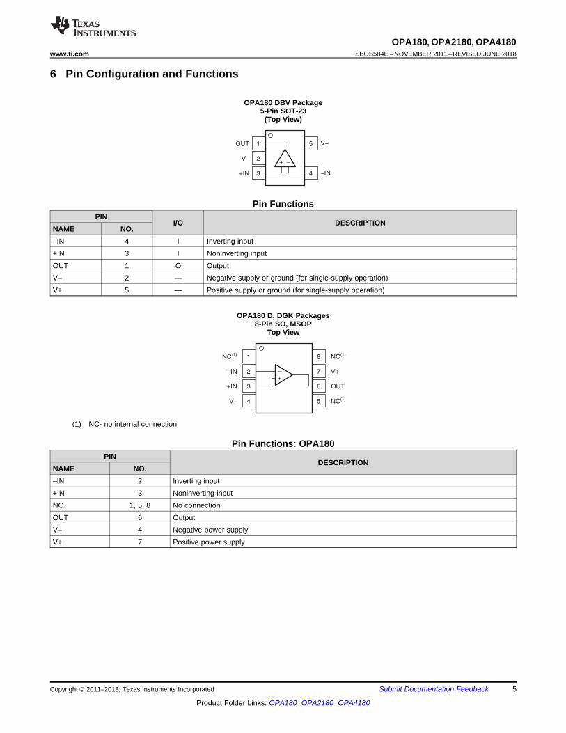
6 Pin Configuration and Functions
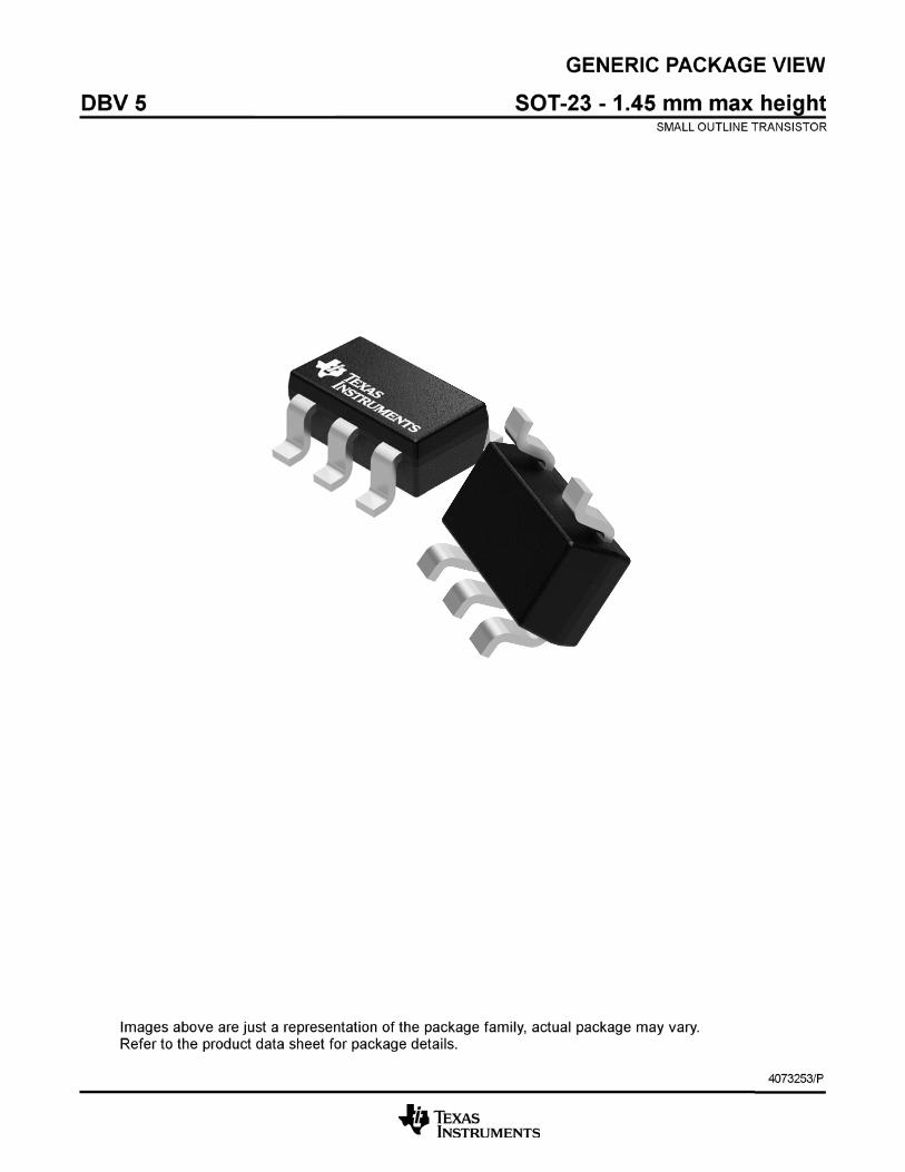
OPA180 DBV Package5-Pin SOT-23
(Top View)
Pin FunctionsPIN
I/O DESCRIPTIONNAME NO.–IN 4 I Inverting input+IN 3 I Noninverting inputOUT 1 O OutputV– 2 — Negative supply or ground (for single-supply operation)V+ 5 — Positive supply or ground (for single-supply operation)
OPA180 D, DGK Packages8-Pin SO, MSOP
Top View
(1) NC- no internal connection
Pin Functions: OPA180PIN
DESCRIPTIONNAME NO.–IN 2 Inverting input+IN 3 Noninverting inputNC 1, 5, 8 No connectionOUT 6 OutputV– 4 Negative power supplyV+ 7 Positive power supply
1
2
3
4
8
7
6
5
V+
OUT B
-IN B
+IN B
OUT A
-IN A
+IN A
V-
A
B
6
OPA180, OPA2180, OPA4180SBOS584E –NOVEMBER 2011–REVISED JUNE 2018 www.ti.com
Product Folder Links: OPA180 OPA2180 OPA4180
Submit Documentation Feedback Copyright © 2011–2018, Texas Instruments Incorporated
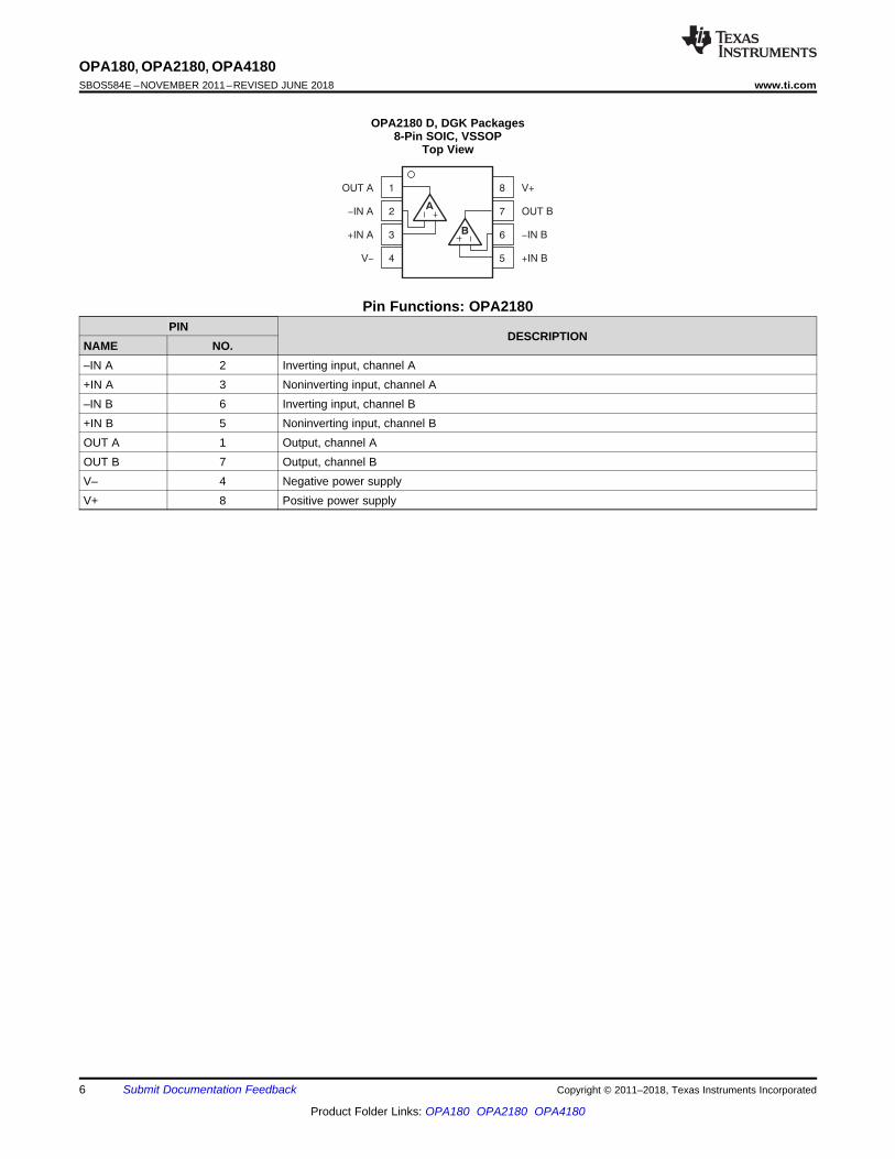
OPA2180 D, DGK Packages8-Pin SOIC, VSSOP
Top View
Pin Functions: OPA2180PIN
DESCRIPTIONNAME NO.–IN A 2 Inverting input, channel A+IN A 3 Noninverting input, channel A–IN B 6 Inverting input, channel B+IN B 5 Noninverting input, channel BOUT A 1 Output, channel AOUT B 7 Output, channel BV– 4 Negative power supplyV+ 8 Positive power supply
1
2
3
4
5
6
7
14
13
12
11
10
9
8
OUT D
-IN D
+IN D
V-
+IN C
-IN C
OUT C
OUT A
-IN A
+IN A
V+
+IN B
-IN B
OUT B
A
B
D
C
7
OPA180, OPA2180, OPA4180www.ti.com SBOS584E –NOVEMBER 2011–REVISED JUNE 2018
Product Folder Links: OPA180 OPA2180 OPA4180
Submit Documentation FeedbackCopyright © 2011–2018, Texas Instruments Incorporated
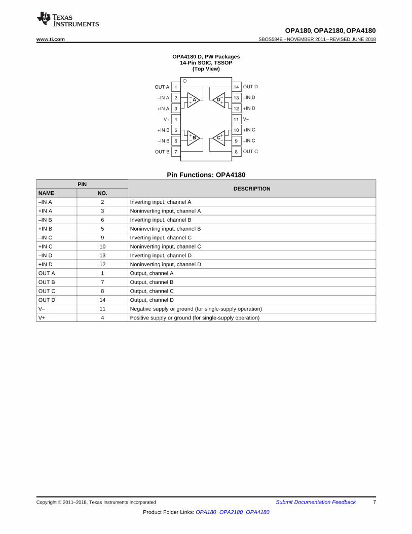
OPA4180 D, PW Packages14-Pin SOIC, TSSOP
(Top View)
Pin Functions: OPA4180PIN
DESCRIPTIONNAME NO.–IN A 2 Inverting input, channel A+IN A 3 Noninverting input, channel A–IN B 6 Inverting input, channel B+IN B 5 Noninverting input, channel B–IN C 9 Inverting input, channel C+IN C 10 Noninverting input, channel C–IN D 13 Inverting input, channel D+IN D 12 Noninverting input, channel DOUT A 1 Output, channel AOUT B 7 Output, channel BOUT C 8 Output, channel COUT D 14 Output, channel DV– 11 Negative supply or ground (for single-supply operation)V+ 4 Positive supply or ground (for single-supply operation)
8
OPA180, OPA2180, OPA4180SBOS584E –NOVEMBER 2011–REVISED JUNE 2018 www.ti.com
Product Folder Links: OPA180 OPA2180 OPA4180
Submit Documentation Feedback Copyright © 2011–2018, Texas Instruments Incorporated
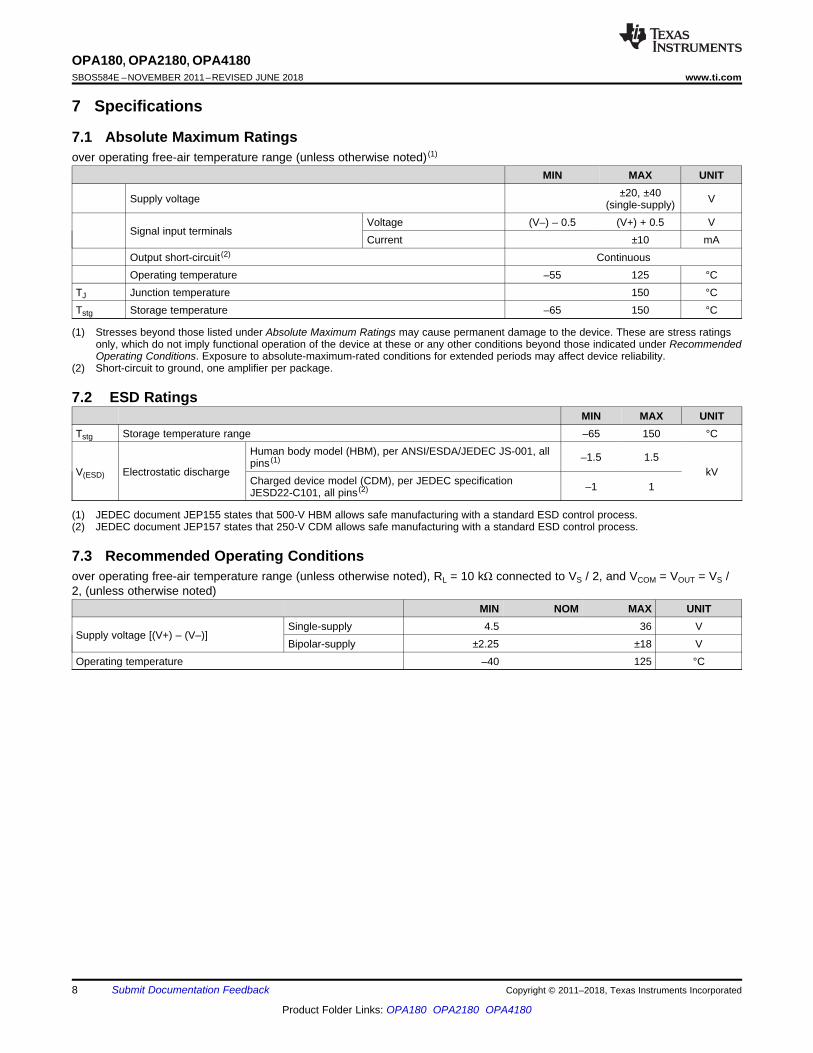
(1) Stresses beyond those listed under Absolute Maximum Ratings may cause permanent damage to the device. These are stress ratingsonly, which do not imply functional operation of the device at these or any other conditions beyond those indicated under RecommendedOperating Conditions. Exposure to absolute-maximum-rated conditions for extended periods may affect device reliability.
(2) Short-circuit to ground, one amplifier per package.
7 Specifications
7.1 Absolute Maximum Ratingsover operating free-air temperature range (unless otherwise noted) (1)
MIN MAX UNIT
Supply voltage ±20, ±40(single-supply) V
Signal input terminalsVoltage (V–) – 0.5 (V+) + 0.5 VCurrent ±10 mA
Output short-circuit (2) ContinuousOperating temperature –55 125 °C
TJ Junction temperature 150 °CTstg Storage temperature –65 150 °C
(1) JEDEC document JEP155 states that 500-V HBM allows safe manufacturing with a standard ESD control process.(2) JEDEC document JEP157 states that 250-V CDM allows safe manufacturing with a standard ESD control process.
7.2 ESD RatingsMIN MAX UNIT
Tstg Storage temperature range –65 150 °C
V(ESD) Electrostatic discharge
Human body model (HBM), per ANSI/ESDA/JEDEC JS-001, allpins (1) –1.5 1.5
kVCharged device model (CDM), per JEDEC specificationJESD22-C101, all pins (2) –1 1
7.3 Recommended Operating Conditionsover operating free-air temperature range (unless otherwise noted), RL = 10 kΩ connected to VS / 2, and VCOM = VOUT = VS /2, (unless otherwise noted)
MIN NOM MAX UNIT
Supply voltage [(V+) – (V–)]Single-supply 4.5 36 VBipolar-supply ±2.25 ±18 V
Operating temperature –40 125 °C
9
OPA180, OPA2180, OPA4180www.ti.com SBOS584E –NOVEMBER 2011–REVISED JUNE 2018
Product Folder Links: OPA180 OPA2180 OPA4180
Submit Documentation FeedbackCopyright © 2011–2018, Texas Instruments Incorporated
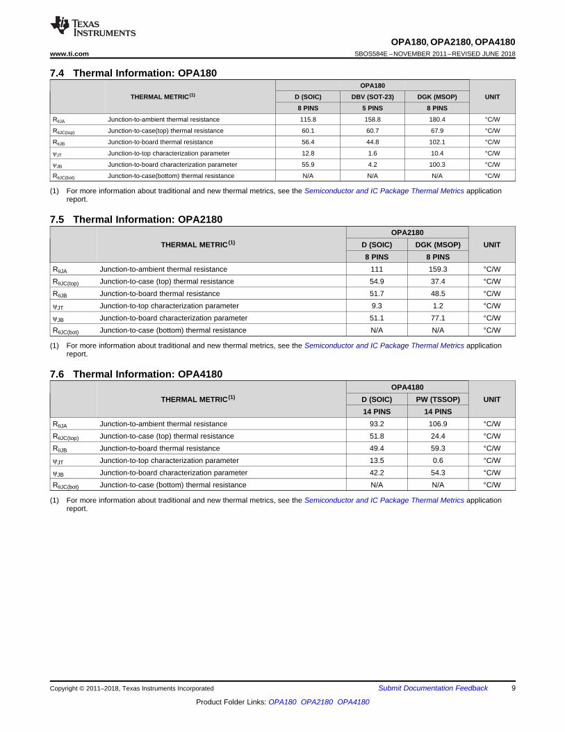
(1) For more information about traditional and new thermal metrics, see the Semiconductor and IC Package Thermal Metrics applicationreport.
7.4 Thermal Information: OPA180
THERMAL METRIC (1)
OPA180
UNITD (SOIC) DBV (SOT-23) DGK (MSOP)
8 PINS 5 PINS 8 PINS
RθJA Junction-to-ambient thermal resistance 115.8 158.8 180.4 °C/W
RθJC(top) Junction-to-case(top) thermal resistance 60.1 60.7 67.9 °C/W
RθJB Junction-to-board thermal resistance 56.4 44.8 102.1 °C/W
ψJT Junction-to-top characterization parameter 12.8 1.6 10.4 °C/W
ψJB Junction-to-board characterization parameter 55.9 4.2 100.3 °C/W
RθJC(bot) Junction-to-case(bottom) thermal resistance N/A N/A N/A °C/W
(1) For more information about traditional and new thermal metrics, see the Semiconductor and IC Package Thermal Metrics applicationreport.
7.5 Thermal Information: OPA2180
THERMAL METRIC (1)OPA2180
UNITD (SOIC) DGK (MSOP)8 PINS 8 PINS
RθJA Junction-to-ambient thermal resistance 111 159.3 °C/WRθJC(top) Junction-to-case (top) thermal resistance 54.9 37.4 °C/WRθJB Junction-to-board thermal resistance 51.7 48.5 °C/WψJT Junction-to-top characterization parameter 9.3 1.2 °C/WψJB Junction-to-board characterization parameter 51.1 77.1 °C/WRθJC(bot) Junction-to-case (bottom) thermal resistance N/A N/A °C/W
(1) For more information about traditional and new thermal metrics, see the Semiconductor and IC Package Thermal Metrics applicationreport.
7.6 Thermal Information: OPA4180
THERMAL METRIC (1)OPA4180
UNITD (SOIC) PW (TSSOP)14 PINS 14 PINS
RθJA Junction-to-ambient thermal resistance 93.2 106.9 °C/WRθJC(top) Junction-to-case (top) thermal resistance 51.8 24.4 °C/WRθJB Junction-to-board thermal resistance 49.4 59.3 °C/WψJT Junction-to-top characterization parameter 13.5 0.6 °C/WψJB Junction-to-board characterization parameter 42.2 54.3 °C/WRθJC(bot) Junction-to-case (bottom) thermal resistance N/A N/A °C/W
10
OPA180, OPA2180, OPA4180SBOS584E –NOVEMBER 2011–REVISED JUNE 2018 www.ti.com
Product Folder Links: OPA180 OPA2180 OPA4180
Submit Documentation Feedback Copyright © 2011–2018, Texas Instruments Incorporated
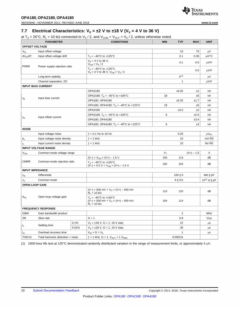
(1) 1000-hour life test at 125°C demonstrated randomly distributed variation in the range of measurement limits, or approximately 4 μV.
7.7 Electrical Characteristics: VS = ±2 V to ±18 V (VS = 4 V to 36 V)at TA = 25°C, RL = 10 kΩ connected to VS / 2, and VCOM = VOUT = VS / 2, unless otherwise noted.
PARAMETER CONDITIONS MIN TYP MAX UNIT
OFFSET VOLTAGE
VIO Input offset voltage 15 75 μV
dVIO/dT Input offset voltage drift TA = –40°C to +125°C 0.1 0.35 μV/°C
PSRR Power supply rejection ratio
VS = 4 V to 36 V,VCM = VS / 2 0.1 0.5 μV/V
TA = –40°C to +125°C,VS = 4 V to 36 V, VCM = VS / 2 0.5 μV/V
Long-term stability 4 (1) μV
Channel separation, DC 1 μV/V
INPUT BIAS CURRENT
IIB Input bias current
OPA2180 ±0.25 ±1 nA
OPA2180: TA = –40°C to +105°C 18 ±5 nA
OPA180, OPA4180 ±0.25 ±1.7 nA
OPA180, OPA4180: TA = –40°C to +125°C 18 ±6 nA
IIO Input offset current
OPA2180 ±0.5 ±2 nA
OPA2180: TA = –40°C to +105°C 6 ±2.5 nA
OPA180, OPA4180 ±3.4 nA
OPA180, OPA4180: TA = –40°C to +125°C 6 ±3 nA
NOISE
Input voltage noise ƒ = 0.1 Hz to 10 Hz 0.25 μVPP
en Input voltage noise density ƒ = 1 kHz 10 nV/√Hz
in Input current noise density ƒ = 1 kHz 10 fA/√Hz
INPUT VOLTAGE RANGE
VCM Common-mode voltage range V– (V+) – 1.5 V
CMRR Common-mode rejection ratio(V–) < VCM < (V+) – 1.5 V 104 114 dB
TA = –40°C to +125°C,(V–) + 0.5 V < VCM < (V+) – 1.5 V 100 104 dB
INPUT IMPEDANCE
zid Differential 100 || 6 MΩ || pF
zic Common-mode 6 || 9.5 1012 Ω || pF
OPEN-LOOP GAIN
AOL Open-loop voltage gain
(V–) + 500 mV < VO < (V+) – 500 mVRL = 10 kΩ 110 120 dB
TA = –40°C to +125°C(V–) + 500 mV < VO < (V+) – 500 mV,RL = 10 kΩ
104 114 dB
FREQUENCY RESPONSE
GBW Gain bandwidth product 2 MHz
SR Slew rate G = 1 0.8 V/μs
ts Settling time0.1% VS = ±18 V, G = 1, 10-V step 22 μs
0.01% VS = ±18 V, G = 1, 10-V step 30 μs
tor Overload recovery time VIN × G = VS 1 μs
THD+N Total harmonic distortion + noise ƒ = 1 kHz, G = 1, VOUT = 1 VRMS 0.0001%
11
OPA180, OPA2180, OPA4180www.ti.com SBOS584E –NOVEMBER 2011–REVISED JUNE 2018
Product Folder Links: OPA180 OPA2180 OPA4180
Submit Documentation FeedbackCopyright © 2011–2018, Texas Instruments Incorporated
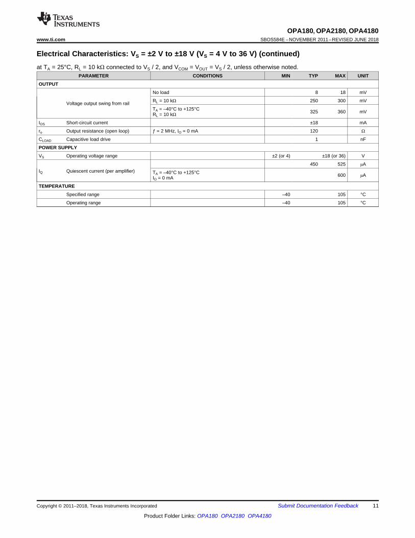
Electrical Characteristics: VS = ±2 V to ±18 V (VS = 4 V to 36 V) (continued)at TA = 25°C, RL = 10 kΩ connected to VS / 2, and VCOM = VOUT = VS / 2, unless otherwise noted.
PARAMETER CONDITIONS MIN TYP MAX UNIT
OUTPUT
Voltage output swing from rail
No load 8 18 mV
RL = 10 kΩ 250 300 mV
TA = –40°C to +125°CRL = 10 kΩ 325 360 mV
IOS Short-circuit current ±18 mA
ro Output resistance (open loop) ƒ = 2 MHz, IO = 0 mA 120 Ω
CLOAD Capacitive load drive 1 nF
POWER SUPPLY
VS Operating voltage range ±2 (or 4) ±18 (or 36) V
IQ Quiescent current (per amplifier)450 525 μA
TA = –40°C to +125°CIO = 0 mA 600 μA
TEMPERATURE
Specified range –40 105 °C
Operating range –40 105 °C
12
OPA180, OPA2180, OPA4180SBOS584E –NOVEMBER 2011–REVISED JUNE 2018 www.ti.com
Product Folder Links: OPA180 OPA2180 OPA4180
Submit Documentation Feedback Copyright © 2011–2018, Texas Instruments Incorporated
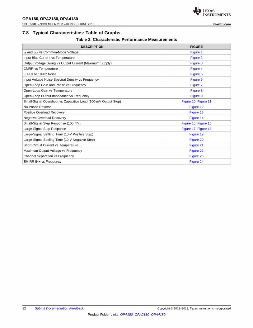
7.8 Typical Characteristics: Table of GraphsTable 2. Characteristic Performance Measurements
DESCRIPTION FIGUREIB and IOS vs Common-Mode Voltage Figure 1Input Bias Current vs Temperature Figure 2Output Voltage Swing vs Output Current (Maximum Supply) Figure 3CMRR vs Temperature Figure 40.1-Hz to 10-Hz Noise Figure 5Input Voltage Noise Spectral Density vs Frequency Figure 6Open-Loop Gain and Phase vs Frequency Figure 7Open-Loop Gain vs Temperature Figure 8Open-Loop Output Impedance vs Frequency Figure 9Small-Signal Overshoot vs Capacitive Load (100-mV Output Step) Figure 10, Figure 11No Phase Reversal Figure 12Positive Overload Recovery Figure 13Negative Overload Recovery Figure 14Small-Signal Step Response (100 mV) Figure 15, Figure 16Large-Signal Step Response Figure 17, Figure 18Large-Signal Settling Time (10-V Positive Step) Figure 19Large-Signal Settling Time (10-V Negative Step) Figure 20Short-Circuit Current vs Temperature Figure 21Maximum Output Voltage vs Frequency Figure 22Channel Separation vs Frequency Figure 23EMIRR IN+ vs Frequency Figure 24
100
10
1
Voltage N
ois
e D
ensity (
nV
/)
ÖH
z
0.1 10 100 1k 10k 100k
Frequency (Hz)
1
50
nV
/div
Time (1 s/div)
20
Ou
tpu
t V
olta
ge
(V
)
0 2 4 6 8 24
Output Current (mA)
10 12 18
17
16
15
14
-14
-15
-16
-17
-20
1614
- °40 C
85 C°
125 C°
2220
19
18
-19
-18
40
35
30
25
20
15
10
5
0
Co
mm
on
-Mo
de
Re
jectio
n R
atio
(V
/V)
m
-55 -35 -15 5 25 125
Temperature ( C)°
45 1058565
(V ) < V < (V+) 1.5 V- CM -
(V ) + 0.5 V < V < (V+) 1.5 V- -CM
500
400
300
200
100
0
100
200
300
-
-
-
Ia
nd I
(pA
)IB
IO
-20 -10 -5 0 5 20
V (V)CM
10-15
+IIB
-IIB
IIO
15
4000
3000
2000
1000
0
1000
2000
-
-
Input B
ias C
urr
ent (p
A)
-55 -35 -15 5 25 125
Temperature ( C)°
45 1058565
IIB+
IIB-
IIO
13
OPA180, OPA2180, OPA4180www.ti.com SBOS584E –NOVEMBER 2011–REVISED JUNE 2018
Product Folder Links: OPA180 OPA2180 OPA4180
Submit Documentation FeedbackCopyright © 2011–2018, Texas Instruments Incorporated
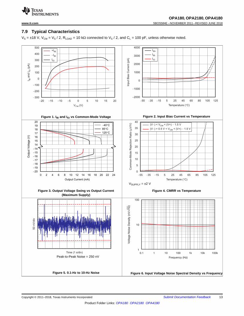
7.9 Typical CharacteristicsVS = ±18 V, VCM = VS / 2, RLOAD = 10 kΩ connected to VS / 2, and CL = 100 pF, unless otherwise noted.
Figure 1. IIB and IIO vs Common-Mode Voltage Figure 2. Input Bias Current vs Temperature
Figure 3. Output Voltage Swing vs Output Current(Maximum Supply)
VSUPPLY = ±2 V
Figure 4. CMRR vs Temperature
Peak-to-Peak Noise = 250 nV
Figure 5. 0.1-Hz to 10-Hz Noise Figure 6. Input Voltage Noise Spectral Density vs Frequency
40
35
30
25
20
15
10
5
0
Overs
hoot (%
)
0 100 200 300 400 500 600 700 800 900 1000
Capacitive Load (pF)
Device
R =I 10 kW
ROUT
CL
RF = 10 kW
18 V
-18 V
G = 1-
R = 0 WOUT
R = 25 WOUT
R = 50 WOUT
Time (100 s/div)m
5 V
/div
18 V
-18 V
37 VPP
Sine Wave
( 18.5 V)±
Device
VI
VO
10k
1k
100
10
1
1m
Z(
)W
O
1 10 100 1k 10k 10M
Frequency (Hz)
100k 1M
40
35
30
25
20
15
10
5
0
Overs
hoot (%
)
0 100 200 300 400 500 600 700 800 900 1000
Capacitive Load (pF)
18 V
-18 V
ROUT
CL
Device
RL
G = 1
R = 0 WOUT
R = 25 WOUT
R = 50 WOUT
3
2.5
2
1.5
1
0.5
0
A(
V/V
)m
OL
-55 -35 -15 5 25 125
Temperature ( C)°
45 1058565
V = 4 V, R = 10 kWSUPPLY L
V = 36 V, R = 10 kWSUPPLY L
10 100 1k 10k 100k 1M 10M 100M−20
0
20
40
60
80
100
120
140
0
45
90
135
180
Frequency (Hz)
Gai
n (d
B)
Pha
se (
°)
GainPhase
G007
14
OPA180, OPA2180, OPA4180SBOS584E –NOVEMBER 2011–REVISED JUNE 2018 www.ti.com
Product Folder Links: OPA180 OPA2180 OPA4180
Submit Documentation Feedback Copyright © 2011–2018, Texas Instruments Incorporated
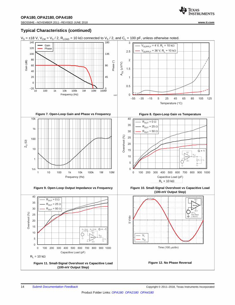
Typical Characteristics (continued)VS = ±18 V, VCM = VS / 2, RLOAD = 10 kΩ connected to VS / 2, and CL = 100 pF, unless otherwise noted.
Figure 7. Open-Loop Gain and Phase vs Frequency Figure 8. Open-Loop Gain vs Temperature
Figure 9. Open-Loop Output Impedance vs Frequency
RL = 10 kΩ
Figure 10. Small-Signal Overshoot vs Capacitive Load(100-mV Output Step)
RL = 10 kΩ
Figure 11. Small-Signal Overshoot vs Capacitive Load(100-mV Output Step)
Figure 12. No Phase Reversal
5 V
/div
Time (50 s/div)m Time (50 s/div)m
5 V
/div
20
mV
/div
Time (1 s/div)m
+18 V
-18 V CLRL
Device
G = 1
Time (20 s/div)m
20
mV
/div
18 V
-18 V
R 2 kWF =R 2 kWI =
CL
Device
G = 1-
Time (5 s/div)m
5 V
/div
VI
VO
2 kW
20 kW
VI
VODevice
G = 10-
18 V
-18 V
Time (5 s/div)m
5 V
/div
VI
VO
2 kW
20 kW
VI
VODevice
G = 10-
18 V
-18 V
15
OPA180, OPA2180, OPA4180www.ti.com SBOS584E –NOVEMBER 2011–REVISED JUNE 2018
Product Folder Links: OPA180 OPA2180 OPA4180
Submit Documentation FeedbackCopyright © 2011–2018, Texas Instruments Incorporated
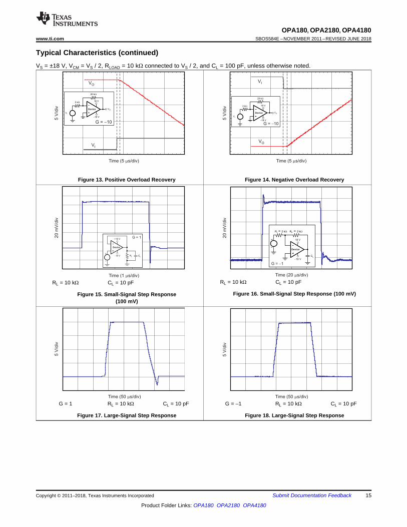
Typical Characteristics (continued)VS = ±18 V, VCM = VS / 2, RLOAD = 10 kΩ connected to VS / 2, and CL = 100 pF, unless otherwise noted.
Figure 13. Positive Overload Recovery Figure 14. Negative Overload Recovery
RL = 10 kΩ CL = 10 pF
Figure 15. Small-Signal Step Response(100 mV)
RL = 10 kΩ CL = 10 pF
Figure 16. Small-Signal Step Response (100 mV)
G = 1 RL = 10 kΩ CL = 10 pF
Figure 17. Large-Signal Step Response
G = –1 RL = 10 kΩ CL = 10 pF
Figure 18. Large-Signal Step Response
-60
70
80
90
100
110
120
130
140
150
-
-
-
-
-
-
-
-
-
Ch
an
ne
l S
ep
ara
tio
n (
dB
)
1 100 1k 10k 100M
Frequency (Hz)
10 100k 1M 10M
Channel A to B
Channel B to A
160
140
120
100
80
60
40
20
0
EM
IRR
IN
+ (
dB
)
10M 10G
Frequency (Hz)
100M 1G
30
20
10
0
10
20
30
-
-
-
I(m
A)
SC
-55 -35 -15 5 25 125
Temperature ( C)°
45 1058565
I , SourceSC
I , SinkSC
15
12.5
10
7.5
5
2.5
0
Ou
tpu
t V
olta
ge
(V
)P
P
1k 100k 1M 10M
Frequency (Hz)
V = 15 V±S
V = 5 V±S
V = 2.25 V±S
Maximum output voltage without
slew-rate induced distortion.
10k
10
8
6
4
2
0
2
4
6
8
10
-
-
-
-
-
Dfr
om
Fin
al V
alu
e (
mV
)
0 60
Time ( s)m
2010 504030
12-Bit Settling
( 1/2 LSB = 0.024%)± ±
10
8
6
4
2
0
2
4
6
8
10
-
-
-
-
-
Dfr
om
Fin
al V
alu
e (
mV
)
0 60
Time ( s)m
2010 504030
12-Bit Settling
( 1/2 LSB = 0.024%)± ±
16
OPA180, OPA2180, OPA4180SBOS584E –NOVEMBER 2011–REVISED JUNE 2018 www.ti.com
Product Folder Links: OPA180 OPA2180 OPA4180
Submit Documentation Feedback Copyright © 2011–2018, Texas Instruments Incorporated
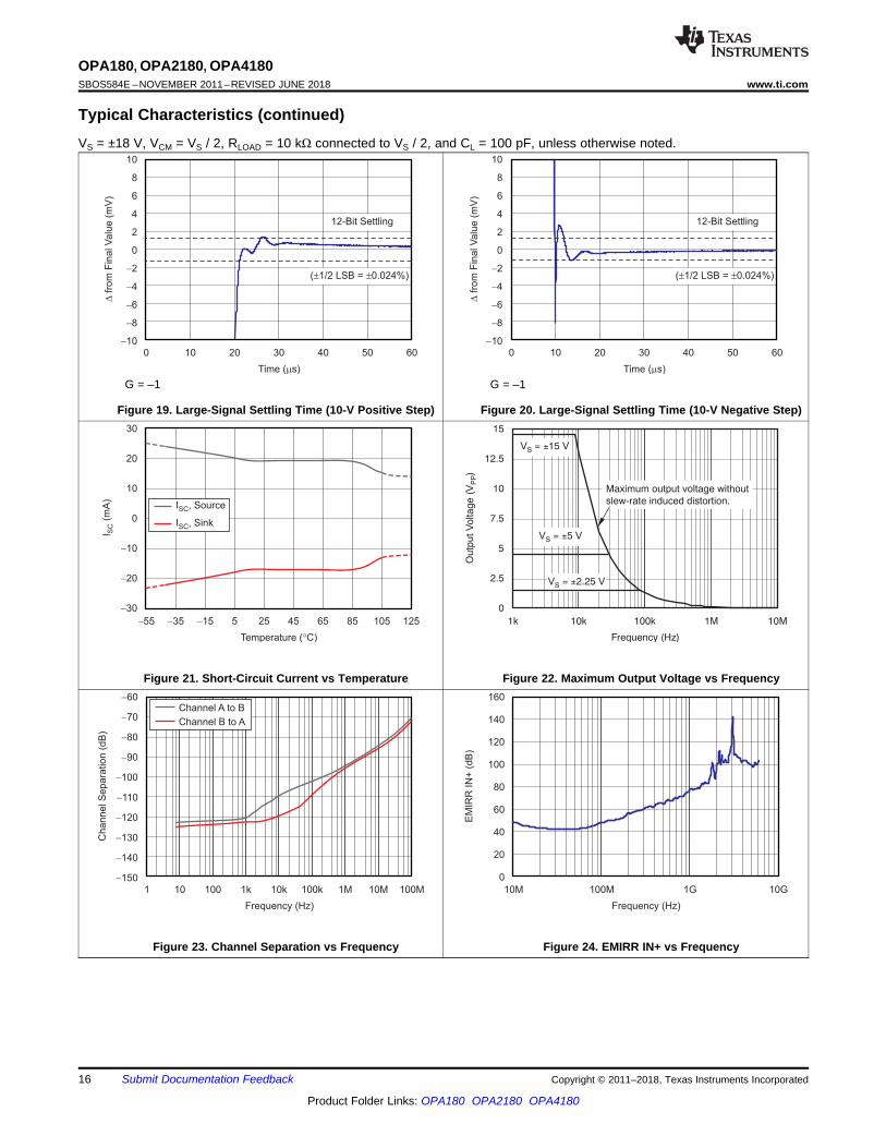
Typical Characteristics (continued)VS = ±18 V, VCM = VS / 2, RLOAD = 10 kΩ connected to VS / 2, and CL = 100 pF, unless otherwise noted.
G = –1
Figure 19. Large-Signal Settling Time (10-V Positive Step)
G = –1
Figure 20. Large-Signal Settling Time (10-V Negative Step)
Figure 21. Short-Circuit Current vs Temperature Figure 22. Maximum Output Voltage vs Frequency
Figure 23. Channel Separation vs Frequency Figure 24. EMIRR IN+ vs Frequency
�
��
��
�
�
�
�
�
GM1
+IN
-IN
CHOP1 CHOP2NotchFilter
GM_FF
GM2 GM3
C2
C1
OUT
V+
V- Copyright © 2017, Texas Instruments Incorporated
17
OPA180, OPA2180, OPA4180www.ti.com SBOS584E –NOVEMBER 2011–REVISED JUNE 2018
Product Folder Links: OPA180 OPA2180 OPA4180
Submit Documentation FeedbackCopyright © 2011–2018, Texas Instruments Incorporated
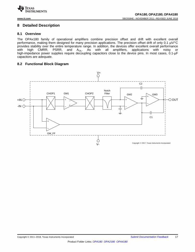
8 Detailed Description
8.1 OverviewThe OPAx180 family of operational amplifiers combine precision offset and drift with excellent overallperformance, making them designed for many precision applications. The precision offset drift of only 0.1 µV/°Cprovides stability over the entire temperature range. In addition, the devices offer excellent overall performancewith high CMRR, PSRR, and AOL. As with all amplifiers, applications with noisy orhigh-impedance power supplies require decoupling capacitors close to the device pins. In most cases, 0.1-µFcapacitors are adequate.
8.2 Functional Block Diagram
Time (100 s/div)m
5 V
/div
18 V
-18 V
37 VPP
Sine Wave
( 18.5 V)±
Device
VI
VO
160
140
120
100
80
60
40
20
0
EM
IRR
IN
+ (
dB
)
10M 10G
Frequency (Hz)
100M 1G
18
OPA180, OPA2180, OPA4180SBOS584E –NOVEMBER 2011–REVISED JUNE 2018 www.ti.com
Product Folder Links: OPA180 OPA2180 OPA4180
Submit Documentation Feedback Copyright © 2011–2018, Texas Instruments Incorporated
8.3 Feature Description
8.3.1 Operating CharacteristicsThe OPAx180 family of amplifiers is specified for operation from 4 V to 36 V (±2 V to ±18 V). Many of thespecifications apply from –40°C to +125°C. Parameters that can exhibit significant variance with regard tooperating voltage or temperature are presented in the Typical Characteristics.
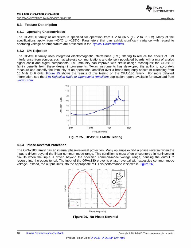
8.3.2 EMI RejectionThe OPAx180 family uses integrated electromagnetic interference (EMI) filtering to reduce the effects of EMIinterference from sources such as wireless communications and densely populated boards with a mix of analogsignal chain and digital components. EMI immunity can improve with circuit design techniques; the OPAx180family benefits from these design improvements. Texas Instruments has developed the ability to accuratelymeasure and quantify the immunity of an operational amplifier over a broad frequency spectrum extending from10 MHz to 6 GHz. Figure 25 shows the results of this testing on the OPAx180 family . For more detailedinformation, see the EMI Rejection Ratio of Operational Amplifiers application report, available for download fromwww.ti.com.
Figure 25. OPAx180 EMIRR Testing
8.3.3 Phase-Reversal ProtectionThe OPAx180 family has an internal phase-reversal protection. Many op amps exhibit a phase reversal when theinput is driven beyond the linear common-mode range. This condition is most often encountered in noninvertingcircuits when the input is driven beyond the specified common-mode voltage range, causing the output toreverse into the opposite rail. The input of the OPAx180 prevents phase reversal with excessive common-modevoltage. Instead, the output limits into the appropriate rail. This performance is shown in Figure 26.
Figure 26. No Phase Reversal
5 kWDevice
10 mA max
V+
VIN
VOUT
IOVERLOAD
40
35
30
25
20
15
10
5
0
Overs
hoot (%
)
0 100 200 300 400 500 600 700 800 900 1000
Capacitive Load (pF)
18 V
-18 V
ROUT
CL
Device
RL
G = 1
R = 0 WOUT
R = 25 WOUT
R = 50 WOUT
40
35
30
25
20
15
10
5
0O
vers
hoot (%
)
0 100 200 300 400 500 600 700 800 900 1000
Capacitive Load (pF)
Device
R =I 10 kW
ROUT
CL
RF = 10 kW
18 V
-18 V
G = 1-
R = 0 WOUT
R = 25 WOUT
R = 50 WOUT
19
OPA180, OPA2180, OPA4180www.ti.com SBOS584E –NOVEMBER 2011–REVISED JUNE 2018
Product Folder Links: OPA180 OPA2180 OPA4180
Submit Documentation FeedbackCopyright © 2011–2018, Texas Instruments Incorporated
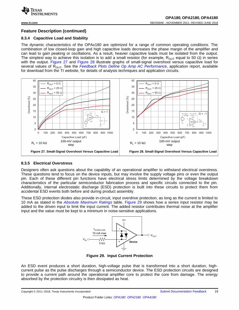
Feature Description (continued)8.3.4 Capacitive Load and StabilityThe dynamic characteristics of the OPAx180 are optimized for a range of common operating conditions. Thecombination of low closed-loop gain and high capacitive loads decreases the phase margin of the amplifier andcan lead to gain peaking or oscillations. As a result, heavier capacitive loads must be isolated from the output.The simplest way to achieve this isolation is to add a small resistor (for example, ROUT equal to 50 Ω) in serieswith the output. Figure 27 and Figure 28 illustrate graphs of small-signal overshoot versus capacitive load forseveral values of ROUT. See the Feedback Plots Define Op Amp AC Performance, application report, availablefor download from the TI website, for details of analysis techniques and application circuits.
RL = 10 kΩ 100-mV outputstep
Figure 27. Small-Signal Overshoot Versus Capacitive Load
RL = 10 kΩ 100-mV outputstep
Figure 28. Small-Signal Overshoot Versus Capacitive Load
8.3.5 Electrical OverstressDesigners often ask questions about the capability of an operational amplifier to withstand electrical overstress.These questions tend to focus on the device inputs, but may involve the supply voltage pins or even the outputpin. Each of these different pin functions have electrical stress limits determined by the voltage breakdowncharacteristics of the particular semiconductor fabrication process and specific circuits connected to the pin.Additionally, internal electrostatic discharge (ESD) protection is built into these circuits to protect them fromaccidental ESD events both before and during product assembly.
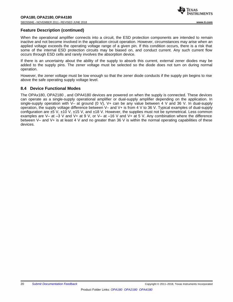
These ESD protection diodes also provide in-circuit, input overdrive protection, as long as the current is limited to10 mA as stated in the Absolute Maximum Ratings table. Figure 29 shows how a series input resistor may beadded to the driven input to limit the input current. The added resistor contributes thermal noise at the amplifierinput and the value must be kept to a minimum in noise-sensitive applications.
Figure 29. Input Current Protection
An ESD event produces a short duration, high-voltage pulse that is transformed into a short duration, high-current pulse as the pulse discharges through a semiconductor device. The ESD protection circuits are designedto provide a current path around the operational amplifier core to protect the core from damage. The energyabsorbed by the protection circuitry is then dissipated as heat.
20
OPA180, OPA2180, OPA4180SBOS584E –NOVEMBER 2011–REVISED JUNE 2018 www.ti.com
Product Folder Links: OPA180 OPA2180 OPA4180
Submit Documentation Feedback Copyright © 2011–2018, Texas Instruments Incorporated
Feature Description (continued)When the operational amplifier connects into a circuit, the ESD protection components are intended to remaininactive and not become involved in the application circuit operation. However, circumstances may arise when anapplied voltage exceeds the operating voltage range of a given pin. If this condition occurs, there is a risk thatsome of the internal ESD protection circuits may be biased on, and conduct current. Any such current flowoccurs through ESD cells and rarely involves the absorption device.
If there is an uncertainty about the ability of the supply to absorb this current, external zener diodes may beadded to the supply pins. The zener voltage must be selected so the diode does not turn on during normaloperation.
However, the zener voltage must be low enough so that the zener diode conducts if the supply pin begins to riseabove the safe operating supply voltage level.
8.4 Device Functional ModesThe OPAx180, OPA2180 , and OPA4180 devices are powered on when the supply is connected. These devicescan operate as a single-supply operational amplifier or dual-supply amplifier depending on the application. Insingle-supply operation with V– at ground (0 V), V+ can be any value between 4 V and 36 V. In dual-supplyoperation, the supply voltage difference between V– and V+ is from 4 V to 36 V. Typical examples of dual-supplyconfiguration are ±5 V, ±10 V, ±15 V, and ±18 V. However, the supplies must not be symmetrical. Less commonexamples are V– at –3 V and V+ at 9 V, or V– at –16 V and V+ at 5 V. Any combination where the differencebetween V– and V+ is at least 4 V and no greater than 36 V is within the normal operating capabilities of thesedevices.
+
RFBRG1
RG2
RISO
CCOMPVREF
VOUT
CLOAD
DAC8560
Device
Copyright © 2017, Texas Instruments Incorporated
21
OPA180, OPA2180, OPA4180www.ti.com SBOS584E –NOVEMBER 2011–REVISED JUNE 2018
Product Folder Links: OPA180 OPA2180 OPA4180
Submit Documentation FeedbackCopyright © 2011–2018, Texas Instruments Incorporated
9 Application and Implementation
9.1 Application InformationThe OPAx180 family offers excellent DC precision and AC performance. These devices operate up to 36-Vsupply rails and offer rail-to-rail output, ultra-low offset voltage, offset voltage drift and 2-MHz bandwidth. Thesefeatures make the OPAx180 a robust, high-performance amplifier for high-voltage industrial applications.
9.2 Typical ApplicationsThese application examples highlight a few of the circuits where the OPAx180 family can be used.
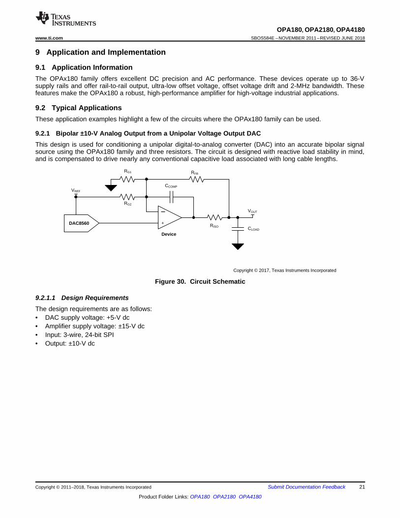
9.2.1 Bipolar ±10-V Analog Output from a Unipolar Voltage Output DACThis design is used for conditioning a unipolar digital-to-analog converter (DAC) into an accurate bipolar signalsource using the OPAx180 family and three resistors. The circuit is designed with reactive load stability in mind,and is compensated to drive nearly any conventional capacitive load associated with long cable lengths.
Figure 30. Circuit Schematic
9.2.1.1 Design RequirementsThe design requirements are as follows:• DAC supply voltage: +5-V dc• Amplifier supply voltage: ±15-V dc• Input: 3-wire, 24-bit SPI• Output: ±10-V dc
22
OPA180, OPA2180, OPA4180SBOS584E –NOVEMBER 2011–REVISED JUNE 2018 www.ti.com
Product Folder Links: OPA180 OPA2180 OPA4180
Submit Documentation Feedback Copyright © 2011–2018, Texas Instruments Incorporated
Typical Applications (continued)9.2.1.2 Detailed Design Procedure
9.2.1.2.1 Component Selection
DAC: For convenience, devices with an external reference option or devices with accessible internal referencesare desirable in this application because the reference creates an offset. The DAC selection in this design mustprimarily be based on DC error contributions typically described by offset error, gain error, and integralnonlinearity error. Occasionally, additional specifications are provided that summarize end-point errors of theDAC typically called zero-code and full-scale errors. For AC applications, slew rate and settling time may requireadditional consideration.
Amplifier: Amplifier input offset voltage (VIO) is a key consideration for this design. VIO of an operational amplifieris a typical data sheet specification, but in-circuit performance is also affected by drift over temperature, thecommon-mode rejection ratio (CMRR), and power-supply rejection ratio (PSRR); thus consideration should begiven to these parameters as well. For ac operation, additional considerations should be made concerning slewrate and settling time. Input bias current (IIB) can also be a factor, but typically the resistor network isimplemented with sufficiently small resistor values that the effects of input bias current are negligible.
Passive: Resistor matching for the op-amp resistor network is critical for the success of this design; componentswith tight tolerances must be selected. For this design, 0.1% resistor values are implemented, but this constraintmay be adjusted based on application-specific design goals. Resistor matching contributes to offset error andgain error in this design; see Bipolar ±10V Analog Output from a Unipolar Voltage Output DAC for further details.The tolerance of the RISOand CCOMP stability components is not critical, and 1% components are acceptable.
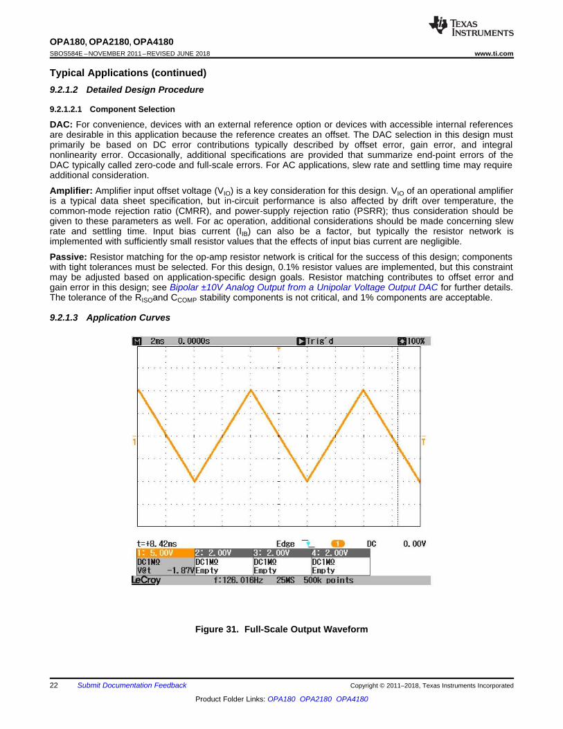
9.2.1.3 Application Curves
Figure 31. Full-Scale Output Waveform
23
OPA180, OPA2180, OPA4180www.ti.com SBOS584E –NOVEMBER 2011–REVISED JUNE 2018
Product Folder Links: OPA180 OPA2180 OPA4180
Submit Documentation FeedbackCopyright © 2011–2018, Texas Instruments Incorporated
Typical Applications (continued)
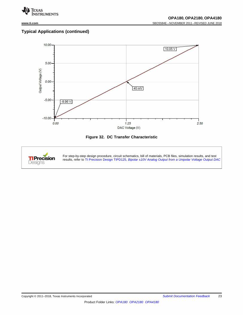
Figure 32. DC Transfer Characteristic
For step-by-step design procedure, circuit schematics, bill of materials, PCB files, simulation results, and testresults, refer to TI Precision Design TIPD125, Bipolar ±10V Analog Output from a Unipolar Voltage Output DAC
+
±
REF5050
1 µFR1
4.99 k �
R2
49.1 k �
R3
60.4 k �
½OPA2180
R5
105.8 k �
R4
1 k �
1 µF
VOUT
RTDPt100
15 V
Out(5 V)
0°C = 0 V200°C = 5 V
In
Copyright © 2017, Texas Instruments Incorporated
½
OPA2180
-15 V
15 V
U5
½
OPA2180
15 V
-15 V
U2
+VCM
10
-VDIFF/2
VDIFF/2 R
1 kW
5
R
1 kW
7R
500 W
G
V POUT
V NOUT
U1
INA159
3.3 V
VOUT
Ref 1
Ref 2
Sense
24
OPA180, OPA2180, OPA4180SBOS584E –NOVEMBER 2011–REVISED JUNE 2018 www.ti.com
Product Folder Links: OPA180 OPA2180 OPA4180
Submit Documentation Feedback Copyright © 2011–2018, Texas Instruments Incorporated
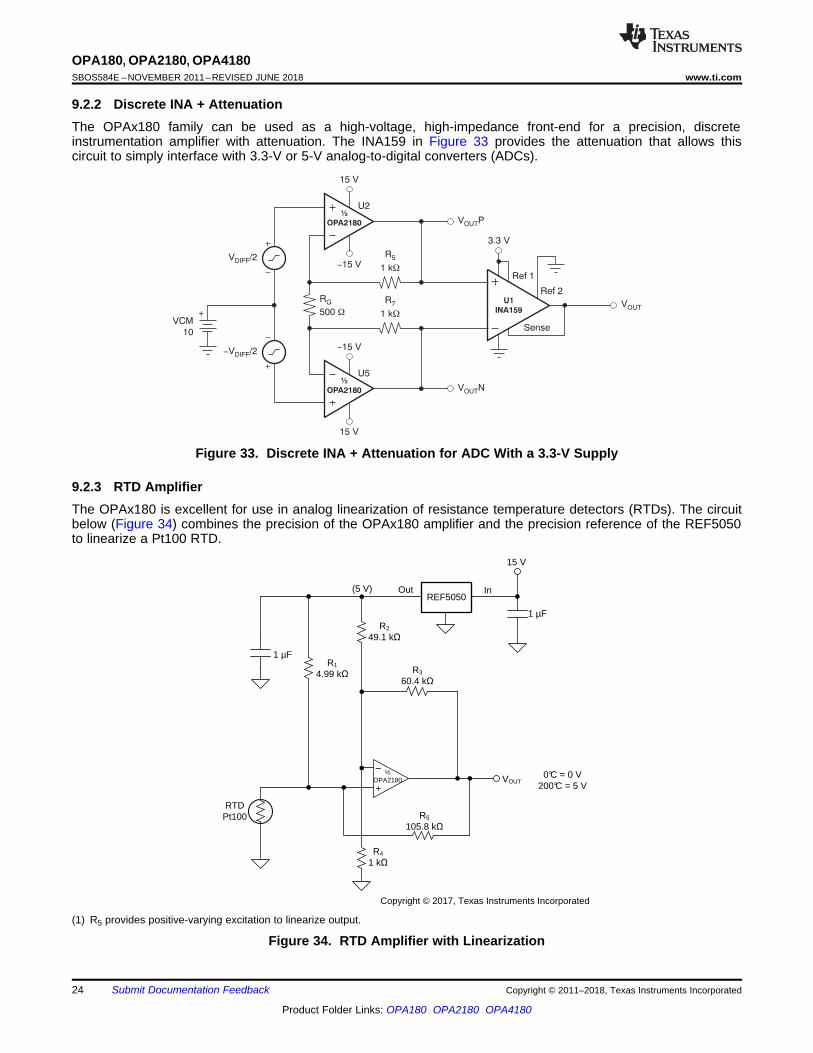
9.2.2 Discrete INA + AttenuationThe OPAx180 family can be used as a high-voltage, high-impedance front-end for a precision, discreteinstrumentation amplifier with attenuation. The INA159 in Figure 33 provides the attenuation that allows thiscircuit to simply interface with 3.3-V or 5-V analog-to-digital converters (ADCs).
Figure 33. Discrete INA + Attenuation for ADC With a 3.3-V Supply
9.2.3 RTD AmplifierThe OPAx180 is excellent for use in analog linearization of resistance temperature detectors (RTDs). The circuitbelow (Figure 34) combines the precision of the OPAx180 amplifier and the precision reference of the REF5050to linearize a Pt100 RTD.
(1) R5 provides positive-varying excitation to linearize output.
Figure 34. RTD Amplifier with Linearization
25
OPA180, OPA2180, OPA4180www.ti.com SBOS584E –NOVEMBER 2011–REVISED JUNE 2018
Product Folder Links: OPA180 OPA2180 OPA4180
Submit Documentation FeedbackCopyright © 2011–2018, Texas Instruments Incorporated
10 Power Supply RecommendationsThe OPAx180 family is specified for operation from 4 V to 36 V (±2 V to ±18 V); many specifications apply from–40°C to +125°C. Parameters that can exhibit significant variance with regard to operating voltage ortemperature are presented in Layout
CAUTIONSupply voltages larger than 40 V can permanently damage the device; see theAbsolute Maximum Ratings.
Place 0.1-μF bypass capacitors close to the power-supply pins to reduce errors coupling in from noisy or high-impedance power supplies. For more detailed information on bypass capacitor placement, see Layout .
NC
±IN
+IN
V±
V+
OUTPUT
NC
NC
VS+
VS± GND
Ground (GND) plane on another layer
VOUT
VIN
GND
Run the input tracesas far away fromthe supply lines
as possible RF
RG
Place components close to device and to each
other to reduce parasitic errors
Use low-ESR, ceramic bypass
capacitor
GND
Use a low-ESR,ceramic bypass
capacitor
26
OPA180, OPA2180, OPA4180SBOS584E –NOVEMBER 2011–REVISED JUNE 2018 www.ti.com
Product Folder Links: OPA180 OPA2180 OPA4180
Submit Documentation Feedback Copyright © 2011–2018, Texas Instruments Incorporated
11 Layout
11.1 Layout GuidelinesFor best operational performance of the device, use good printed circuit board (PCB) layout practices, including:
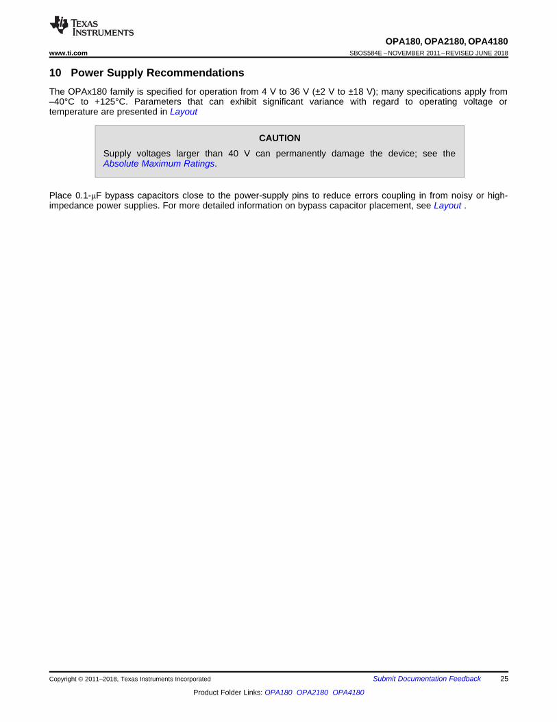
• Noise can propagate into analog circuitry through the power pins of the circuit as a whole and op ampitself. Bypass capacitors are used to reduce the coupled noise by providing low-impedance powersources local to the analog circuitry.– Connect low-ESR, 0.1-µF ceramic bypass capacitors between each supply pin and ground, placed as
close to the device as possible. A single bypass capacitor from V+ to ground is applicable for single-supply applications.
• Separate grounding for analog and digital portions of circuitry is one of the simplest and most-effectivemethods of noise suppression. One or more layers on multilayer PCBs are typically devoted to groundplanes. A ground plane helps distribute heat and reduces EMI noise pickup. Take care to physicallyseparate digital and analog grounds, paying attention to the flow of the ground current.
• In order to reduce parasitic coupling, run the input traces as far away from the supply or output traces aspossible. If it is not possible to keep the input traces separate, it is much better to cross the sensitivetrace perpendicular as opposed to in parallel with the noisy trace.
• Place the external components as close to the device as possible. As shown in Figure 35, keeping RFand RG close to the inverting input minimizes parasitic capacitance.
• Keep the length of input traces as short as possible. Always remember that the input traces are the mostsensitive part of the circuit.
• Consider a driven, low-impedance guard ring around the critical traces. A guard ring can significantlyreduce leakage currents from nearby traces that are at different potentials.
11.2 Layout Example
Figure 35. Operational Amplifier Board Layout for Noninverting Configuration
27
OPA180, OPA2180, OPA4180www.ti.com SBOS584E –NOVEMBER 2011–REVISED JUNE 2018
Product Folder Links: OPA180 OPA2180 OPA4180
Submit Documentation FeedbackCopyright © 2011–2018, Texas Instruments Incorporated
12 Device and Documentation Support
12.1 Related LinksTable 3 lists quick access links. Categories include technical documents, support and community resources,tools and software, and quick access to sample or buy.
Table 3. Related Links
PARTS PRODUCT FOLDER ORDER NOW TECHNICALDOCUMENTS
TOOLS &SOFTWARE
SUPPORT &COMMUNITY
OPA180 Click here Click here Click here Click here Click hereOPA2180 Click here Click here Click here Click here Click hereOPA4180 Click here Click here Click here Click here Click here
12.2 TrademarksAll trademarks are the property of their respective owners.
12.3 Electrostatic Discharge CautionThese devices have limited built-in ESD protection. The leads should be shorted together or the device placed in conductive foamduring storage or handling to prevent electrostatic damage to the MOS gates.
12.4 GlossarySLYZ022 — TI Glossary.
This glossary lists and explains terms, acronyms, and definitions.
13 Mechanical, Packaging, and Orderable InformationThe following pages include mechanical, packaging, and orderable information. This information is the mostcurrent data available for the designated devices. This data is subject to change without notice and revision ofthis document. For browser-based versions of this data sheet, refer to the left-hand navigation.
PACKAGE OPTION ADDENDUM
www.ti.com 11-Oct-2016
Addendum-Page 1
PACKAGING INFORMATION
Orderable Device Status(1)
Package Type PackageDrawing
Pins PackageQty
Eco Plan(2)
Lead/Ball Finish(6)
MSL Peak Temp(3)
Op Temp (°C) Device Marking(4/5)
Samples
OPA180ID ACTIVE SOIC D 8 75 Green (RoHS& no Sb/Br)
CU NIPDAU Level-2-260C-1 YEAR -40 to 105 OPA180
OPA180IDBVR ACTIVE SOT-23 DBV 5 3000 Green (RoHS& no Sb/Br)
CU NIPDAU Level-2-260C-1 YEAR -40 to 105 SHJ
OPA180IDBVT ACTIVE SOT-23 DBV 5 250 Green (RoHS& no Sb/Br)
CU NIPDAU Level-2-260C-1 YEAR -40 to 105 SHJ
OPA180IDGKR ACTIVE VSSOP DGK 8 2500 Green (RoHS& no Sb/Br)
CU NIPDAU Level-2-260C-1 YEAR -40 to 105 SHK
OPA180IDGKT ACTIVE VSSOP DGK 8 250 Green (RoHS& no Sb/Br)
CU NIPDAU Level-2-260C-1 YEAR -40 to 105 SHK
OPA180IDR ACTIVE SOIC D 8 2500 Green (RoHS& no Sb/Br)
CU NIPDAU Level-2-260C-1 YEAR -40 to 105 OPA180
OPA2180ID ACTIVE SOIC D 8 75 Green (RoHS& no Sb/Br)
CU NIPDAU Level-2-260C-1 YEAR -40 to 105 2180
OPA2180IDGK ACTIVE VSSOP DGK 8 80 Green (RoHS& no Sb/Br)
CU NIPDAUAG Level-2-260C-1 YEAR -40 to 105 2180
OPA2180IDGKR ACTIVE VSSOP DGK 8 2500 Green (RoHS& no Sb/Br)
CU NIPDAUAG Level-2-260C-1 YEAR -40 to 105 2180
OPA2180IDR ACTIVE SOIC D 8 2500 Green (RoHS& no Sb/Br)
CU NIPDAU Level-2-260C-1 YEAR -40 to 105 2180
OPA4180ID ACTIVE SOIC D 14 50 Green (RoHS& no Sb/Br)
CU NIPDAU Level-2-260C-1 YEAR -40 to 105 OPA4180
OPA4180IDR ACTIVE SOIC D 14 2500 Green (RoHS& no Sb/Br)
CU NIPDAU Level-2-260C-1 YEAR -40 to 105 OPA4180
OPA4180IPW ACTIVE TSSOP PW 14 90 Green (RoHS& no Sb/Br)
CU NIPDAU Level-2-260C-1 YEAR -40 to 105 OPA4180
OPA4180IPWR ACTIVE TSSOP PW 14 2000 Green (RoHS& no Sb/Br)
CU NIPDAU Level-2-260C-1 YEAR -40 to 105 OPA4180
(1) The marketing status values are defined as follows:ACTIVE: Product device recommended for new designs.LIFEBUY: TI has announced that the device will be discontinued, and a lifetime-buy period is in effect.NRND: Not recommended for new designs. Device is in production to support existing customers, but TI does not recommend using this part in a new design.PREVIEW: Device has been announced but is not in production. Samples may or may not be available.OBSOLETE: TI has discontinued the production of the device.
PACKAGE OPTION ADDENDUM
www.ti.com 11-Oct-2016
Addendum-Page 2
(2) Eco Plan - The planned eco-friendly classification: Pb-Free (RoHS), Pb-Free (RoHS Exempt), or Green (RoHS & no Sb/Br) - please check http://www.ti.com/productcontent for the latest availabilityinformation and additional product content details.TBD: The Pb-Free/Green conversion plan has not been defined.Pb-Free (RoHS): TI's terms "Lead-Free" or "Pb-Free" mean semiconductor products that are compatible with the current RoHS requirements for all 6 substances, including the requirement thatlead not exceed 0.1% by weight in homogeneous materials. Where designed to be soldered at high temperatures, TI Pb-Free products are suitable for use in specified lead-free processes.Pb-Free (RoHS Exempt): This component has a RoHS exemption for either 1) lead-based flip-chip solder bumps used between the die and package, or 2) lead-based die adhesive used betweenthe die and leadframe. The component is otherwise considered Pb-Free (RoHS compatible) as defined above.Green (RoHS & no Sb/Br): TI defines "Green" to mean Pb-Free (RoHS compatible), and free of Bromine (Br) and Antimony (Sb) based flame retardants (Br or Sb do not exceed 0.1% by weightin homogeneous material)
(3) MSL, Peak Temp. - The Moisture Sensitivity Level rating according to the JEDEC industry standard classifications, and peak solder temperature.
(4) There may be additional marking, which relates to the logo, the lot trace code information, or the environmental category on the device.
(5) Multiple Device Markings will be inside parentheses. Only one Device Marking contained in parentheses and separated by a "~" will appear on a device. If a line is indented then it is a continuationof the previous line and the two combined represent the entire Device Marking for that device.
(6) Lead/Ball Finish - Orderable Devices may have multiple material finish options. Finish options are separated by a vertical ruled line. Lead/Ball Finish values may wrap to two lines if the finishvalue exceeds the maximum column width.
Important Information and Disclaimer:The information provided on this page represents TI's knowledge and belief as of the date that it is provided. TI bases its knowledge and belief on informationprovided by third parties, and makes no representation or warranty as to the accuracy of such information. Efforts are underway to better integrate information from third parties. TI has taken andcontinues to take reasonable steps to provide representative and accurate information but may not have conducted destructive testing or chemical analysis on incoming materials and chemicals.TI and TI suppliers consider certain information to be proprietary, and thus CAS numbers and other limited information may not be available for release.
In no event shall TI's liability arising out of such information exceed the total purchase price of the TI part(s) at issue in this document sold by TI to Customer on an annual basis.
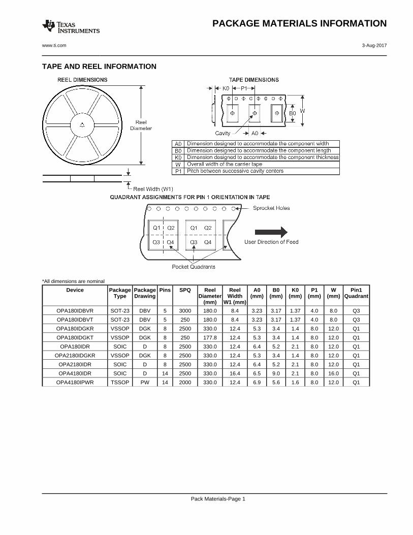
TAPE AND REEL INFORMATION
*All dimensions are nominal
Device PackageType
PackageDrawing
Pins SPQ ReelDiameter
(mm)
ReelWidth
W1 (mm)
A0(mm)
B0(mm)
K0(mm)
P1(mm)
W(mm)
Pin1Quadrant
OPA180IDBVR SOT-23 DBV 5 3000 180.0 8.4 3.23 3.17 1.37 4.0 8.0 Q3
OPA180IDBVT SOT-23 DBV 5 250 180.0 8.4 3.23 3.17 1.37 4.0 8.0 Q3
OPA180IDGKR VSSOP DGK 8 2500 330.0 12.4 5.3 3.4 1.4 8.0 12.0 Q1
OPA180IDGKT VSSOP DGK 8 250 177.8 12.4 5.3 3.4 1.4 8.0 12.0 Q1
OPA180IDR SOIC D 8 2500 330.0 12.4 6.4 5.2 2.1 8.0 12.0 Q1
OPA2180IDGKR VSSOP DGK 8 2500 330.0 12.4 5.3 3.4 1.4 8.0 12.0 Q1
OPA2180IDR SOIC D 8 2500 330.0 12.4 6.4 5.2 2.1 8.0 12.0 Q1
OPA4180IDR SOIC D 14 2500 330.0 16.4 6.5 9.0 2.1 8.0 16.0 Q1
OPA4180IPWR TSSOP PW 14 2000 330.0 12.4 6.9 5.6 1.6 8.0 12.0 Q1
PACKAGE MATERIALS INFORMATION
www.ti.com 3-Aug-2017
Pack Materials-Page 1
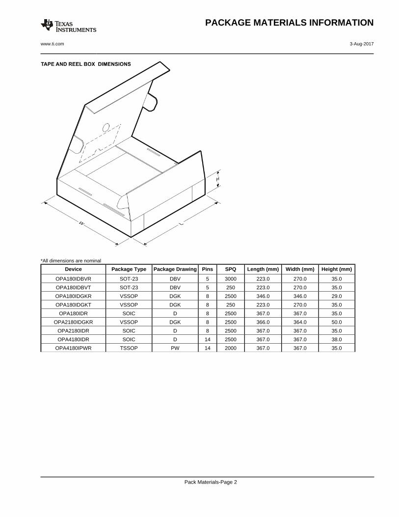
*All dimensions are nominal
Device Package Type Package Drawing Pins SPQ Length (mm) Width (mm) Height (mm)
OPA180IDBVR SOT-23 DBV 5 3000 223.0 270.0 35.0
OPA180IDBVT SOT-23 DBV 5 250 223.0 270.0 35.0
OPA180IDGKR VSSOP DGK 8 2500 346.0 346.0 29.0
OPA180IDGKT VSSOP DGK 8 250 223.0 270.0 35.0
OPA180IDR SOIC D 8 2500 367.0 367.0 35.0
OPA2180IDGKR VSSOP DGK 8 2500 366.0 364.0 50.0
OPA2180IDR SOIC D 8 2500 367.0 367.0 35.0
OPA4180IDR SOIC D 14 2500 367.0 367.0 38.0
OPA4180IPWR TSSOP PW 14 2000 367.0 367.0 35.0
PACKAGE MATERIALS INFORMATION
www.ti.com 3-Aug-2017
Pack Materials-Page 2
www.ti.com
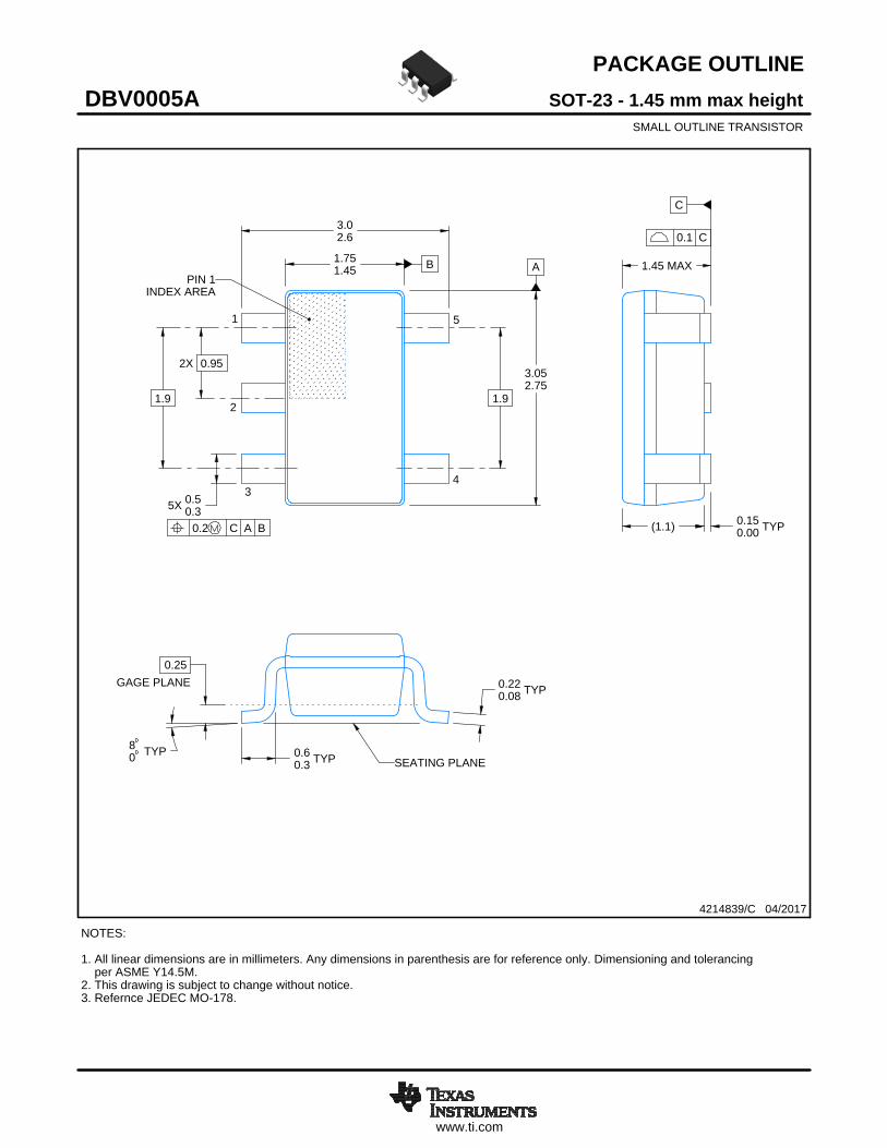
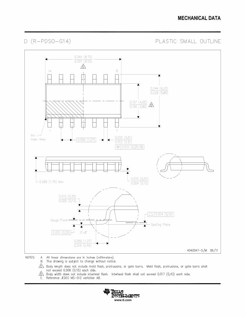
PACKAGE OUTLINE
C
TYP0.220.08
0.25
3.02.6
2X 0.95
1.9
1.45 MAX
TYP0.150.00
5X 0.50.3
TYP0.60.3
TYP80
1.9
A
3.052.75
B1.751.45
(1.1)
SOT-23 - 1.45 mm max heightDBV0005ASMALL OUTLINE TRANSISTOR
4214839/C 04/2017
NOTES: 1. All linear dimensions are in millimeters. Any dimensions in parenthesis are for reference only. Dimensioning and tolerancing per ASME Y14.5M.2. This drawing is subject to change without notice.3. Refernce JEDEC MO-178.
0.2 C A B
1
34
5
2
INDEX AREAPIN 1
GAGE PLANE
SEATING PLANE
0.1 C
SCALE 4.000
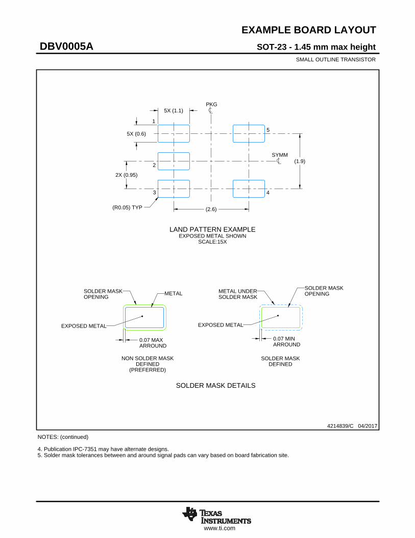
www.ti.com
EXAMPLE BOARD LAYOUT
0.07 MAXARROUND
0.07 MINARROUND
5X (1.1)
5X (0.6)
(2.6)
(1.9)
2X (0.95)
(R0.05) TYP
4214839/C 04/2017
SOT-23 - 1.45 mm max heightDBV0005ASMALL OUTLINE TRANSISTOR
NOTES: (continued) 4. Publication IPC-7351 may have alternate designs. 5. Solder mask tolerances between and around signal pads can vary based on board fabrication site.
SYMM
LAND PATTERN EXAMPLEEXPOSED METAL SHOWN
SCALE:15X
PKG
1
3 4
5
2
SOLDER MASKOPENINGMETAL UNDER
SOLDER MASK
SOLDER MASKDEFINED
EXPOSED METAL
METALSOLDER MASKOPENING
NON SOLDER MASKDEFINED
(PREFERRED)
SOLDER MASK DETAILS
EXPOSED METAL
www.ti.com
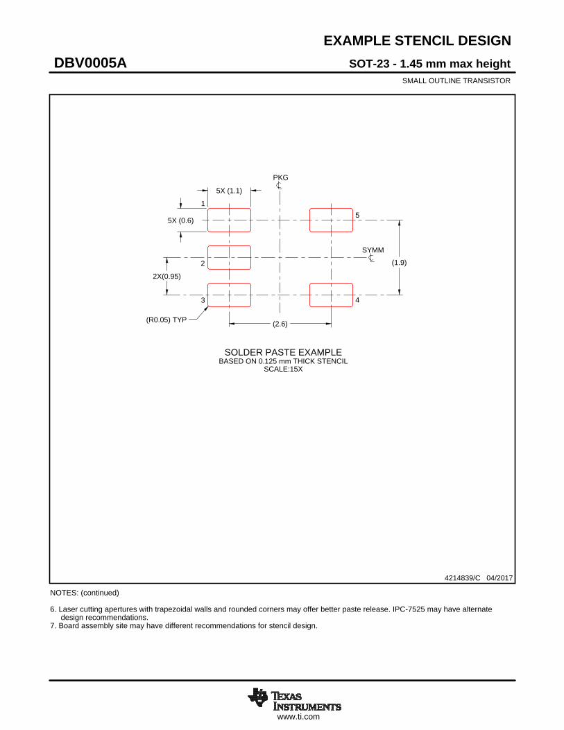
EXAMPLE STENCIL DESIGN
(2.6)
(1.9)
2X(0.95)
5X (1.1)
5X (0.6)
(R0.05) TYP
SOT-23 - 1.45 mm max heightDBV0005ASMALL OUTLINE TRANSISTOR
4214839/C 04/2017
NOTES: (continued) 6. Laser cutting apertures with trapezoidal walls and rounded corners may offer better paste release. IPC-7525 may have alternate design recommendations. 7. Board assembly site may have different recommendations for stencil design.
SOLDER PASTE EXAMPLEBASED ON 0.125 mm THICK STENCIL
SCALE:15X
SYMM
PKG
1
3 4
5
2

www.ti.com
PACKAGE OUTLINE
C
TYP0.220.08
0.25
3.02.6
2X 0.95
1.9
1.45 MAX
TYP0.150.00
5X 0.50.3
TYP0.60.3
TYP80
1.9
A
3.052.75
B1.751.45
(1.1)
SOT-23 - 1.45 mm max heightDBV0005ASMALL OUTLINE TRANSISTOR
4214839/C 04/2017
NOTES: 1. All linear dimensions are in millimeters. Any dimensions in parenthesis are for reference only. Dimensioning and tolerancing per ASME Y14.5M.2. This drawing is subject to change without notice.3. Refernce JEDEC MO-178.
0.2 C A B
1
34
5
2
INDEX AREAPIN 1
GAGE PLANE
SEATING PLANE
0.1 C
SCALE 4.000

www.ti.com
EXAMPLE BOARD LAYOUT
0.07 MAXARROUND
0.07 MINARROUND
5X (1.1)
5X (0.6)
(2.6)
(1.9)
2X (0.95)
(R0.05) TYP
4214839/C 04/2017
SOT-23 - 1.45 mm max heightDBV0005ASMALL OUTLINE TRANSISTOR
NOTES: (continued) 4. Publication IPC-7351 may have alternate designs. 5. Solder mask tolerances between and around signal pads can vary based on board fabrication site.
SYMM
LAND PATTERN EXAMPLEEXPOSED METAL SHOWN
SCALE:15X
PKG
1
3 4
5
2
SOLDER MASKOPENINGMETAL UNDER
SOLDER MASK
SOLDER MASKDEFINED
EXPOSED METAL
METALSOLDER MASKOPENING
NON SOLDER MASKDEFINED
(PREFERRED)
SOLDER MASK DETAILS
EXPOSED METAL

www.ti.com
EXAMPLE STENCIL DESIGN
(2.6)
(1.9)
2X(0.95)
5X (1.1)
5X (0.6)
(R0.05) TYP
SOT-23 - 1.45 mm max heightDBV0005ASMALL OUTLINE TRANSISTOR
4214839/C 04/2017
NOTES: (continued) 6. Laser cutting apertures with trapezoidal walls and rounded corners may offer better paste release. IPC-7525 may have alternate design recommendations. 7. Board assembly site may have different recommendations for stencil design.
SOLDER PASTE EXAMPLEBASED ON 0.125 mm THICK STENCIL
SCALE:15X
SYMM
PKG
1
3 4
5
2
IMPORTANT NOTICE
Texas Instruments Incorporated (TI) reserves the right to make corrections, enhancements, improvements and other changes to itssemiconductor products and services per JESD46, latest issue, and to discontinue any product or service per JESD48, latest issue. Buyersshould obtain the latest relevant information before placing orders and should verify that such information is current and complete.TI’s published terms of sale for semiconductor products (http://www.ti.com/sc/docs/stdterms.htm) apply to the sale of packaged integratedcircuit products that TI has qualified and released to market. Additional terms may apply to the use or sale of other types of TI products andservices.Reproduction of significant portions of TI information in TI data sheets is permissible only if reproduction is without alteration and isaccompanied by all associated warranties, conditions, limitations, and notices. TI is not responsible or liable for such reproduceddocumentation. Information of third parties may be subject to additional restrictions. Resale of TI products or services with statementsdifferent from or beyond the parameters stated by TI for that product or service voids all express and any implied warranties for theassociated TI product or service and is an unfair and deceptive business practice. TI is not responsible or liable for any such statements.Buyers and others who are developing systems that incorporate TI products (collectively, “Designers”) understand and agree that Designersremain responsible for using their independent analysis, evaluation and judgment in designing their applications and that Designers havefull and exclusive responsibility to assure the safety of Designers' applications and compliance of their applications (and of all TI productsused in or for Designers’ applications) with all applicable regulations, laws and other applicable requirements. Designer represents that, withrespect to their applications, Designer has all the necessary expertise to create and implement safeguards that (1) anticipate dangerousconsequences of failures, (2) monitor failures and their consequences, and (3) lessen the likelihood of failures that might cause harm andtake appropriate actions. Designer agrees that prior to using or distributing any applications that include TI products, Designer willthoroughly test such applications and the functionality of such TI products as used in such applications.TI’s provision of technical, application or other design advice, quality characterization, reliability data or other services or information,including, but not limited to, reference designs and materials relating to evaluation modules, (collectively, “TI Resources”) are intended toassist designers who are developing applications that incorporate TI products; by downloading, accessing or using TI Resources in anyway, Designer (individually or, if Designer is acting on behalf of a company, Designer’s company) agrees to use any particular TI Resourcesolely for this purpose and subject to the terms of this Notice.TI’s provision of TI Resources does not expand or otherwise alter TI’s applicable published warranties or warranty disclaimers for TIproducts, and no additional obligations or liabilities arise from TI providing such TI Resources. TI reserves the right to make corrections,enhancements, improvements and other changes to its TI Resources. TI has not conducted any testing other than that specificallydescribed in the published documentation for a particular TI Resource.Designer is authorized to use, copy and modify any individual TI Resource only in connection with the development of applications thatinclude the TI product(s) identified in such TI Resource. NO OTHER LICENSE, EXPRESS OR IMPLIED, BY ESTOPPEL OR OTHERWISETO ANY OTHER TI INTELLECTUAL PROPERTY RIGHT, AND NO LICENSE TO ANY TECHNOLOGY OR INTELLECTUAL PROPERTYRIGHT OF TI OR ANY THIRD PARTY IS GRANTED HEREIN, including but not limited to any patent right, copyright, mask work right, orother intellectual property right relating to any combination, machine, or process in which TI products or services are used. Informationregarding or referencing third-party products or services does not constitute a license to use such products or services, or a warranty orendorsement thereof. Use of TI Resources may require a license from a third party under the patents or other intellectual property of thethird party, or a license from TI under the patents or other intellectual property of TI.TI RESOURCES ARE PROVIDED “AS IS” AND WITH ALL FAULTS. TI DISCLAIMS ALL OTHER WARRANTIES ORREPRESENTATIONS, EXPRESS OR IMPLIED, REGARDING RESOURCES OR USE THEREOF, INCLUDING BUT NOT LIMITED TOACCURACY OR COMPLETENESS, TITLE, ANY EPIDEMIC FAILURE WARRANTY AND ANY IMPLIED WARRANTIES OFMERCHANTABILITY, FITNESS FOR A PARTICULAR PURPOSE, AND NON-INFRINGEMENT OF ANY THIRD PARTY INTELLECTUALPROPERTY RIGHTS. TI SHALL NOT BE LIABLE FOR AND SHALL NOT DEFEND OR INDEMNIFY DESIGNER AGAINST ANY CLAIM,INCLUDING BUT NOT LIMITED TO ANY INFRINGEMENT CLAIM THAT RELATES TO OR IS BASED ON ANY COMBINATION OFPRODUCTS EVEN IF DESCRIBED IN TI RESOURCES OR OTHERWISE. IN NO EVENT SHALL TI BE LIABLE FOR ANY ACTUAL,DIRECT, SPECIAL, COLLATERAL, INDIRECT, PUNITIVE, INCIDENTAL, CONSEQUENTIAL OR EXEMPLARY DAMAGES INCONNECTION WITH OR ARISING OUT OF TI RESOURCES OR USE THEREOF, AND REGARDLESS OF WHETHER TI HAS BEENADVISED OF THE POSSIBILITY OF SUCH DAMAGES.Unless TI has explicitly designated an individual product as meeting the requirements of a particular industry standard (e.g., ISO/TS 16949and ISO 26262), TI is not responsible for any failure to meet such industry standard requirements.Where TI specifically promotes products as facilitating functional safety or as compliant with industry functional safety standards, suchproducts are intended to help enable customers to design and create their own applications that meet applicable functional safety standardsand requirements. Using products in an application does not by itself establish any safety features in the application. Designers mustensure compliance with safety-related requirements and standards applicable to their applications. Designer may not use any TI products inlife-critical medical equipment unless authorized officers of the parties have executed a special contract specifically governing such use.Life-critical medical equipment is medical equipment where failure of such equipment would cause serious bodily injury or death (e.g., lifesupport, pacemakers, defibrillators, heart pumps, neurostimulators, and implantables). Such equipment includes, without limitation, allmedical devices identified by the U.S. Food and Drug Administration as Class III devices and equivalent classifications outside the U.S.TI may expressly designate certain products as completing a particular qualification (e.g., Q100, Military Grade, or Enhanced Product).Designers agree that it has the necessary expertise to select the product with the appropriate qualification designation for their applicationsand that proper product selection is at Designers’ own risk. Designers are solely responsible for compliance with all legal and regulatoryrequirements in connection with such selection.Designer will fully indemnify TI and its representatives against any damages, costs, losses, and/or liabilities arising out of Designer’s non-compliance with the terms and provisions of this Notice.
Mailing Address: Texas Instruments, Post Office Box 655303, Dallas, Texas 75265Copyright © 2018, Texas Instruments Incorporated


![FμP EÒÍõm] Aø©¨¦PÎß ©UPÒ ¤μv{vPÐUPõÚ Book - Uratchikal Mepattu...t.v©](https://static.fdocument.org/doc/165x107/5b1fd4af7f8b9a20508b61ad/fp-eoiom-aopiss-upo-vvpdupou-book-uratchikal-mepattutv.jpg)