Octal Edge-Triggered D-Type Flip-Flops With 3-State ...
21
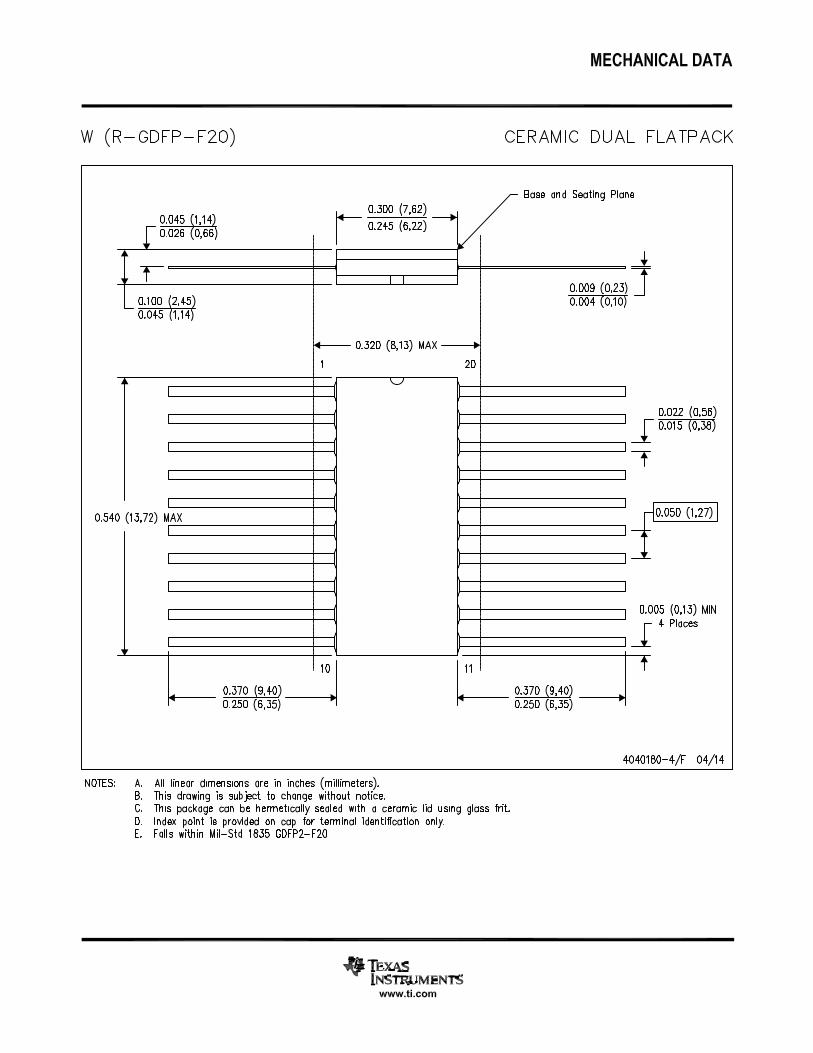
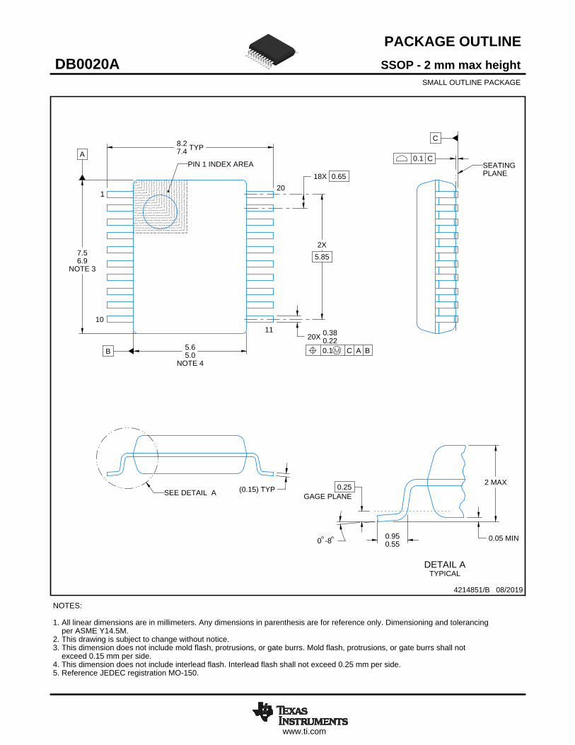
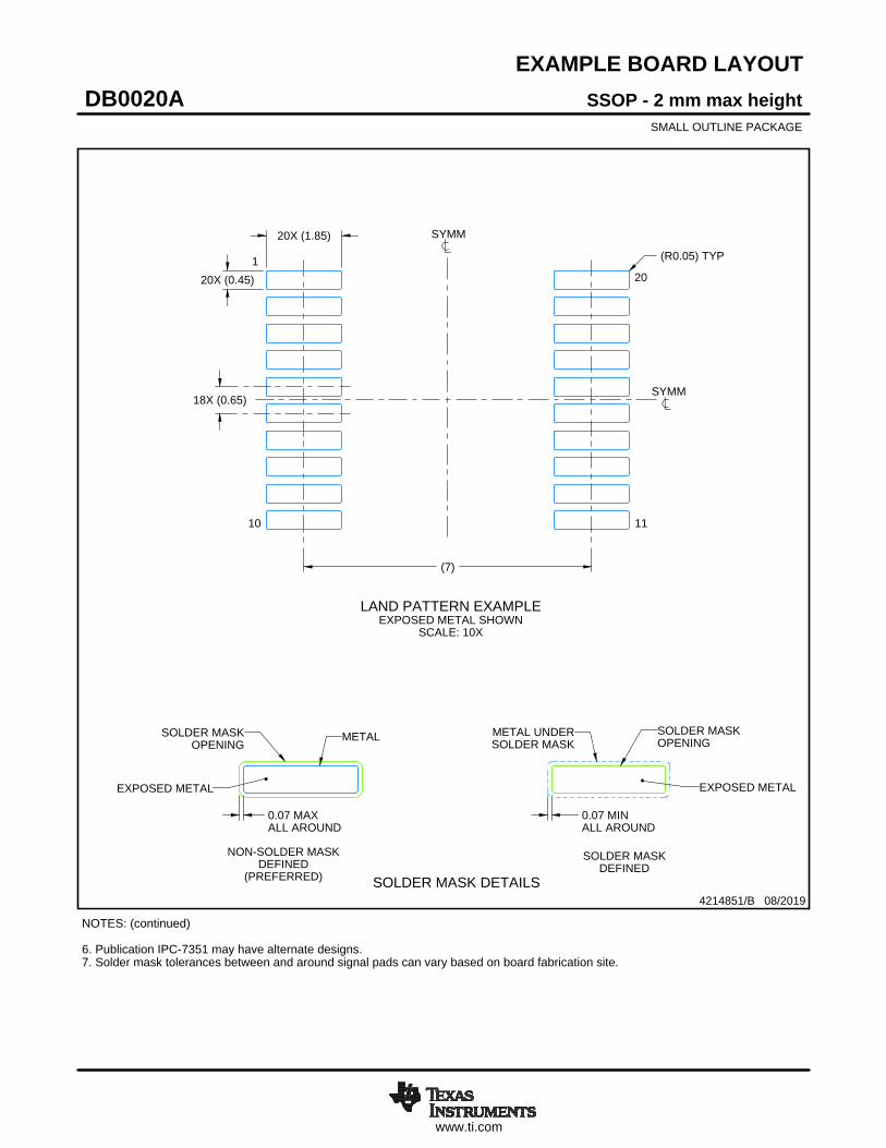
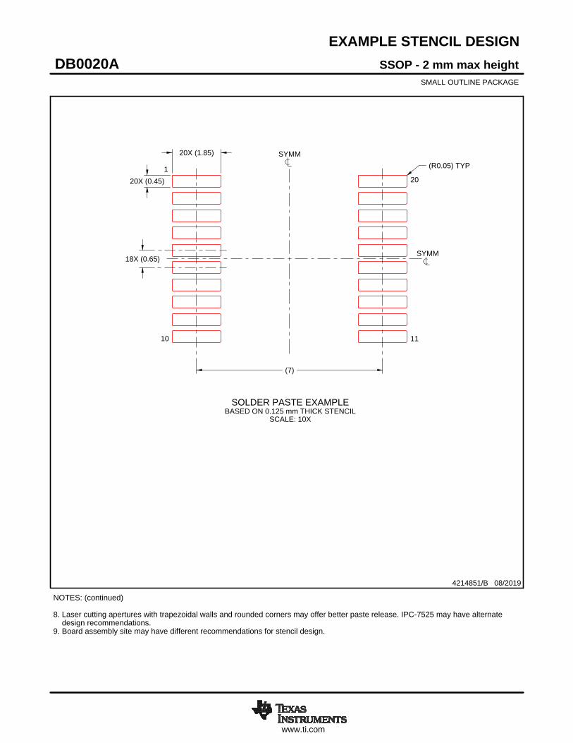
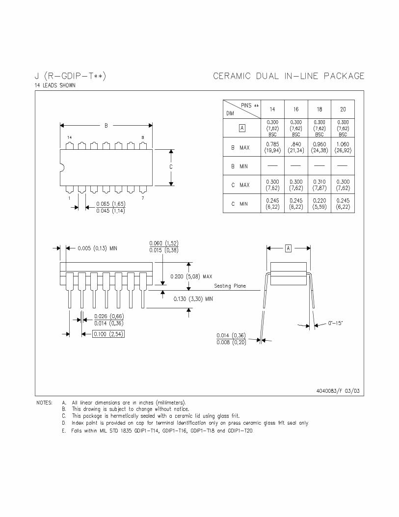
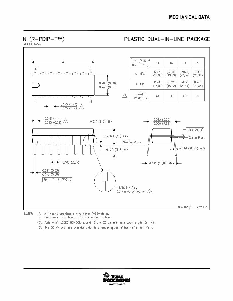
SN54ABT534, SN74ABT534A OCTAL EDGE-TRIGGERED D-TYPE FLIP-FLOPS WITH 3-STATE OUTPUTS SCBS187F – JANUARY 1991 – REVISED JANUARY 1997 1 POST OFFICE BOX 655303 • DALLAS, TEXAS 75265 State-of-the-Art EPIC-ΙΙB BiCMOS Design Significantly Reduces Power Dissipation Latch-Up Performance Exceeds 500 mA Per JEDEC Standard JESD-17 Typical V OLP (Output Ground Bounce) < 1 V at V CC = 5 V, T A = 25°C High-Drive Outputs (–32-mA I OH , 64-mA I OL ) ESD Protection Exceeds 2000 V Per MIL-STD-883, Method 3015; Exceeds 200 V Using Machine Model (C = 200 pF, R = 0) Package Options Include Plastic Small-Outline (DW), Shrink Small-Outline (DB), and Thin Shrink Small-Outline (PW) Packages, Ceramic Chip Carriers (FK), Plastic (N) and Ceramic (J) DIPs, and Ceramic Flat (W) Package description These 8-bit flip-flops with 3-state outputs are designed specifically for driving highly capacitive or relatively low-impedance loads. They are particularly suitable for implementing buffer registers, I/O ports, bidirectional bus drivers, and working registers. The eight flip-flops are edge-triggered D-type flip-flops. On the positive transition of the clock (CLK), the Q outputs are set to the complement of the logic levels set up at the data (D) inputs. A buffered output-enable (OE ) input can be used to place the eight outputs in either a normal logic state (high or low logic levels) or a high-impedance state. In the high-impedance state, the outputs neither load nor drive the bus lines significantly. The high-impedance state and increased drive provide the capability to drive bus lines without need for interface or pullup components. OE does not affect the internal operations of the flip-flop. Previously stored data can be retained or new data can be entered while the outputs are in the high-impedance state. To ensure the high-impedance state during power up or power down, OE should be tied to V CC through a pullup resistor; the minimum value of the resistor is determined by the current-sinking capability of the driver. The SN54ABT534 is characterized for operation over the full military temperature range of –55°C to 125°C. The SN74ABT534A is characterized for operation from –40°C to 85°C. Copyright 1997, Texas Instruments Incorporated PRODUCTION DATA information is current as of publication date. Products conform to specifications per the terms of Texas Instruments standard warranty. Production processing does not necessarily include testing of all parameters. Please be aware that an important notice concerning availability, standard warranty, and use in critical applications of Texas Instruments semiconductor products and disclaimers thereto appears at the end of this data sheet. EPIC-ΙΙB is a trademark of Texas Instruments Incorporated. 1 2 3 4 5 6 7 8 9 10 20 19 18 17 16 15 14 13 12 11 OE 1Q 1D 2D 2Q 3Q 3D 4D 4Q GND V CC 8Q 8D 7D 7Q 6Q 6D 5D 5Q CLK SN54ABT534 . . . J OR W PACKAGE SN74ABT534A . . . DB, DW, N, OR PW PACKAGE (TOP VIEW) 3 2 1 20 19 9 10 11 12 13 4 5 6 7 8 18 17 16 15 14 8D 7D 7Q 6Q 6D 2D 2Q 3Q 3D 4D SN54ABT534 . . . FK PACKAGE (TOP VIEW) 1D 1Q OE 5Q 5D 8Q 4Q GND CLK V CC
Transcript of Octal Edge-Triggered D-Type Flip-Flops With 3-State ...
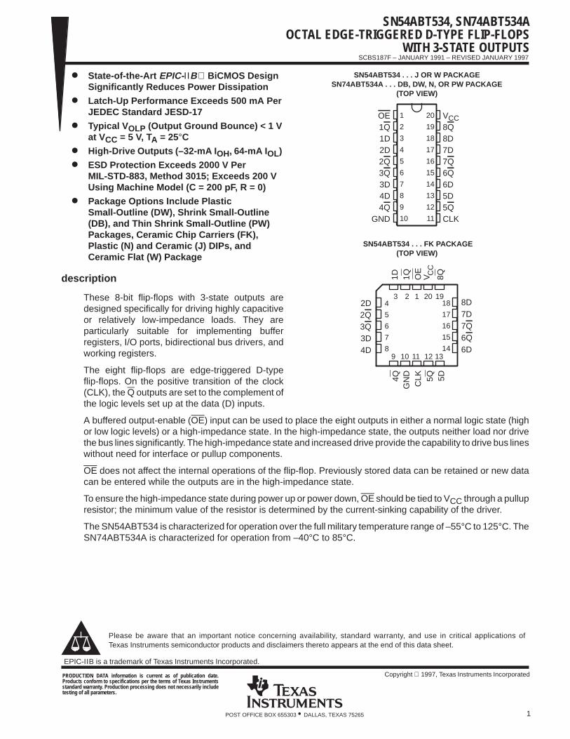
SN54ABT534, SN74ABT534AOCTAL EDGE-TRIGGERED D-TYPE FLIP-FLOPS
WITH 3-STATE OUTPUTS
SCBS187F – JANUARY 1991 – REVISED JANUARY 1997
1POST OFFICE BOX 655303 • DALLAS, TEXAS 75265
State-of-the-Art EPIC-ΙΙB BiCMOS DesignSignificantly Reduces Power Dissipation
Latch-Up Performance Exceeds 500 mA PerJEDEC Standard JESD-17
Typical V OLP (Output Ground Bounce) < 1 Vat VCC = 5 V, TA = 25°C
High-Drive Outputs (–32-mA I OH, 64-mA IOL)
ESD Protection Exceeds 2000 V PerMIL-STD-883, Method 3015; Exceeds 200 VUsing Machine Model (C = 200 pF, R = 0)
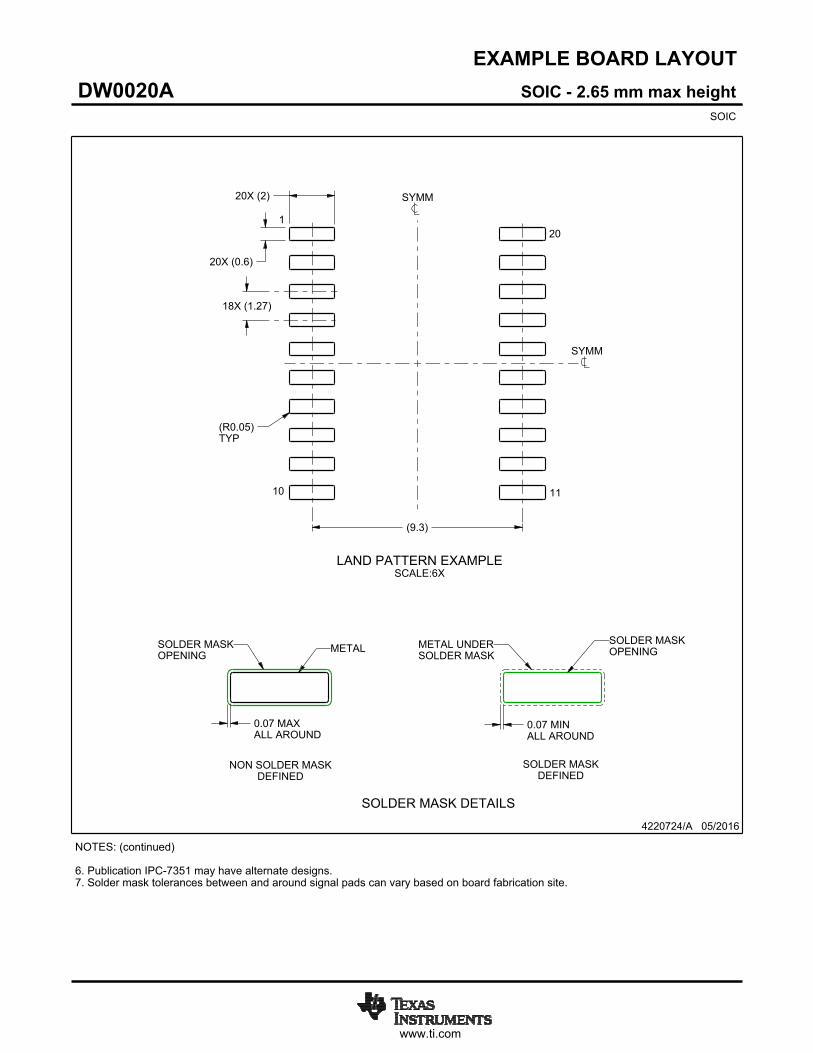
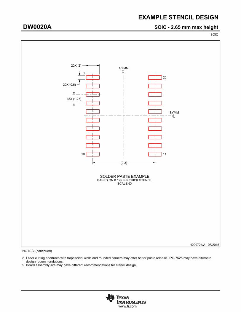
Package Options Include PlasticSmall-Outline (DW), Shrink Small-Outline(DB), and Thin Shrink Small-Outline (PW)Packages, Ceramic Chip Carriers (FK),Plastic (N) and Ceramic (J) DIPs, andCeramic Flat (W) Package
description
These 8-bit flip-flops with 3-state outputs aredesigned specifically for driving highly capacitiveor relatively low-impedance loads. They areparticularly suitable for implementing bufferregisters, I/O ports, bidirectional bus drivers, andworking registers.
The eight flip-flops are edge-triggered D-typeflip-flops. On the positive transition of the clock(CLK), the Q outputs are set to the complement ofthe logic levels set up at the data (D) inputs.
A buffered output-enable (OE) input can be used to place the eight outputs in either a normal logic state (highor low logic levels) or a high-impedance state. In the high-impedance state, the outputs neither load nor drivethe bus lines significantly. The high-impedance state and increased drive provide the capability to drive bus lineswithout need for interface or pullup components.
OE does not affect the internal operations of the flip-flop. Previously stored data can be retained or new datacan be entered while the outputs are in the high-impedance state.
To ensure the high-impedance state during power up or power down, OE should be tied to VCC through a pullupresistor; the minimum value of the resistor is determined by the current-sinking capability of the driver.
The SN54ABT534 is characterized for operation over the full military temperature range of –55°C to 125°C. TheSN74ABT534A is characterized for operation from –40°C to 85°C.
Copyright 1997, Texas Instruments IncorporatedPRODUCTION DATA information is current as of publication date.Products conform to specifications per the terms of Texas Instrumentsstandard warranty. Production processing does not necessarily includetesting of all parameters.
Please be aware that an important notice concerning availability, standard warranty, and use in critical applications ofTexas Instruments semiconductor products and disclaimers thereto appears at the end of this data sheet.
EPIC-ΙΙB is a trademark of Texas Instruments Incorporated.
1
2
3
4
5
6
7
8
9
10
20
19
18
17
16
15
14
13
12
11
OE1Q1D2D2Q3Q3D4D4Q
GND
VCC8Q8D7D7Q6Q6D5D5QCLK
SN54ABT534 . . . J OR W PACKAGESN74ABT534A . . . DB, DW, N, OR PW PACKAGE
(TOP VIEW)
3 2 1 20 19
9 10 11 12 13
4
5
6
7
8
18
17
16
15
14
8D7D7Q6Q6D
2D2Q3Q3D4D
SN54ABT534 . . . FK PACKAGE(TOP VIEW)
1D 1Q OE
5Q 5D8Q
4QG
ND
CLK
V CC
SN54ABT534, SN74ABT534AOCTAL EDGE-TRIGGERED D-TYPE FLIP-FLOPSWITH 3-STATE OUTPUTS
SCBS187F – JANUARY 1991 – REVISED JANUARY 1997
2 POST OFFICE BOX 655303 • DALLAS, TEXAS 75265
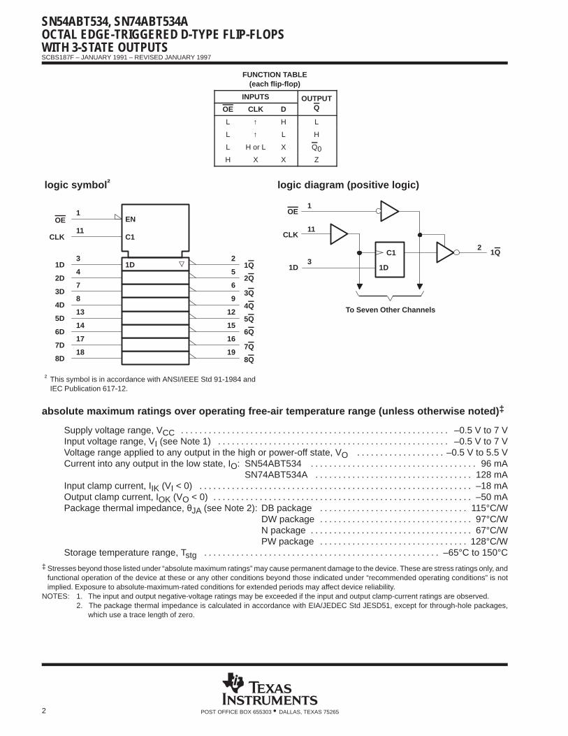
FUNCTION TABLE(each flip-flop)
INPUTS OUTPUTOE CLK D Q
L ↑ H L
L ↑ L H
L H or L X Q0
H X X Z
logic symbol †
† This symbol is in accordance with ANSI/IEEE Std 91-1984 andIEC Publication 617-12.
1D3
1D4
2D7
3D8
4D13
5D14
6D17
7D18
8D
2
5
6
9
12
15
16
19
EN1
C111
CLK
OE
1Q
2Q
3Q
4Q
5Q
6Q
8Q
7Q
logic diagram (positive logic)
1D
C1
OE
1D
1Q
CLK
1
11
3
2
To Seven Other Channels
absolute maximum ratings over operating free-air temperature range (unless otherwise noted) ‡
Supply voltage range, VCC –0.5 V to 7 V. . . . . . . . . . . . . . . . . . . . . . . . . . . . . . . . . . . . . . . . . . . . . . . . . . . . . . . . . . Input voltage range, VI (see Note 1) –0.5 V to 7 V. . . . . . . . . . . . . . . . . . . . . . . . . . . . . . . . . . . . . . . . . . . . . . . . . . Voltage range applied to any output in the high or power-off state, VO –0.5 V to 5.5 V. . . . . . . . . . . . . . . . . . . Current into any output in the low state, IO: SN54ABT534 96 mA. . . . . . . . . . . . . . . . . . . . . . . . . . . . . . . . . . . .
SN74ABT534A 128 mA. . . . . . . . . . . . . . . . . . . . . . . . . . . . . . . . . . Input clamp current, IIK (VI < 0) –18 mA. . . . . . . . . . . . . . . . . . . . . . . . . . . . . . . . . . . . . . . . . . . . . . . . . . . . . . . . . . . Output clamp current, IOK (VO < 0) –50 mA. . . . . . . . . . . . . . . . . . . . . . . . . . . . . . . . . . . . . . . . . . . . . . . . . . . . . . . . Package thermal impedance, θJA (see Note 2): DB package 115°C/W. . . . . . . . . . . . . . . . . . . . . . . . . . . . . . . .
DW package 97°C/W. . . . . . . . . . . . . . . . . . . . . . . . . . . . . . . . . N package 67°C/W. . . . . . . . . . . . . . . . . . . . . . . . . . . . . . . . . . . PW package 128°C/W. . . . . . . . . . . . . . . . . . . . . . . . . . . . . . . .
Storage temperature range, Tstg –65°C to 150°C. . . . . . . . . . . . . . . . . . . . . . . . . . . . . . . . . . . . . . . . . . . . . . . . . . .
‡ Stresses beyond those listed under “absolute maximum ratings” may cause permanent damage to the device. These are stress ratings only, andfunctional operation of the device at these or any other conditions beyond those indicated under “recommended operating conditions” is notimplied. Exposure to absolute-maximum-rated conditions for extended periods may affect device reliability.
NOTES: 1. The input and output negative-voltage ratings may be exceeded if the input and output clamp-current ratings are observed.2. The package thermal impedance is calculated in accordance with EIA/JEDEC Std JESD51, except for through-hole packages,
which use a trace length of zero.
SN54ABT534, SN74ABT534AOCTAL EDGE-TRIGGERED D-TYPE FLIP-FLOPS
WITH 3-STATE OUTPUTS
SCBS187F – JANUARY 1991 – REVISED JANUARY 1997
3POST OFFICE BOX 655303 • DALLAS, TEXAS 75265
recommended operating conditions (see Note 3)
SN54ABT534 SN74ABT534AUNIT
MAX MIN MAXUNIT
VCC Supply voltage 4.5 5.5 4.5 5.5 V
VIH High-level input voltage 2 2 V
VIL Low-level input voltage 0.8 0.8 V
VI Input voltage 0 VCC 0 VCC V
IOH High-level output current –24 –32 mA
IOL Low-level output current 48 64 mA
∆t/∆v Input transition rise or fall rate Outputs enabled 5 5 ns/V
TA Operating free-air temperature –55 125 –40 85 °C
NOTE 3: Unused inputs must be held high or low to prevent them from floating.
electrical characteristics over recommended operating free-air temperature range (unlessotherwise noted)
PARAMETER TEST CONDITIONSTA = 25°C SN54ABT534 SN74ABT534A
UNITPARAMETER TEST CONDITIONSMIN TYP† MAX MIN MAX MIN MAX
UNIT
VIK VCC = 4.5 V, II = –18 mA –1.2 –1.2 –1.2 V
VCC = 4.5 V, IOH = –3 mA 2.5 2.5 2.5
VOHVCC = 5 V, IOH = –3 mA 3 3 3
VVOHVCC = 4 5 V
IOH = –24 mA 2 2V
VCC = 4.5 VIOH = –32 mA 2* 2
VOL VCC = 4 5 VIOL = 48 mA 0.55 0.55
VVOL VCC = 4.5 VIOL = 64 mA 0.55* 0.55
V
Vhys 100 mV
II VCC = 5.5 V, VI = VCC or GND ±1 ±1 ±1 µA
IOZH VCC = 5.5 V, VO = 2.7 V 10‡ 10‡ 10‡ µA
IOZL VCC = 5.5 V, VO = 0.5 V –10‡ –10‡ –10‡ µA
Ioff VCC = 0, VI or VO ≤ 4.5 V ±100 ±100 µA
ICEX VCC = 5.5 V, VO = 5.5 V Outputs high 50 50 50 µA
IO§ VCC = 5.5 V, VO = 2.5 V –50 –100 –180‡ –50 –180‡ –50 –180‡ mA
V 5 5 V I 0Outputs high 1 250 250 250 µA
ICCVCC = 5.5 V, IO = 0,VI = VCC or GND
Outputs low 24 30 30 30 mAVI = VCC or GND
Outputs disabled 0.5 250 250 250 µA
∆ICC¶ VCC = 5.5 V, One input at 3.4 V,Other inputs at VCC or GND
1.5 1.5 1.5 mA
Ci VI = 2.5 V or 0.5 V 3.5 pF
Co VO = 2.5 V or 0.5 V 6.5 pF
* On products compliant to MIL-PRF-38535, this parameter does not apply.† All typical values are at VCC = 5 V.‡ This data sheet limit may vary among suppliers.§ Not more than one output should be tested at a time, and the duration of the test should not exceed one second.¶ This is the increase in supply current for each input that is at the specified TTL voltage level rather than VCC or GND.
SN54ABT534, SN74ABT534AOCTAL EDGE-TRIGGERED D-TYPE FLIP-FLOPSWITH 3-STATE OUTPUTS
SCBS187F – JANUARY 1991 – REVISED JANUARY 1997
4 POST OFFICE BOX 655303 • DALLAS, TEXAS 75265
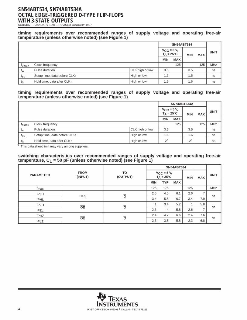
timing requirements over recommended ranges of supply voltage and operating free-airtemperature (unless otherwise noted) (see Figure 1)
SN54ABT534
VCC = 5 V,TA = 25°C MIN MAX
UNIT
MIN MAX
fclock Clock frequency 125 125 MHz
tw Pulse duration CLK high or low 3.5 3.5 ns
tsu Setup time, data before CLK↑ High or low 1.6 1.6 ns
th Hold time, data after CLK↑ High or low 1.6 1.6 ns
timing requirements over recommended ranges of supply voltage and operating free-airtemperature (unless otherwise noted) (see Figure 1)
SN74ABT534A
VCC = 5 V,TA = 25°C MIN MAX
UNIT
MIN MAX
fclock Clock frequency 125 125 MHz
tw Pulse duration CLK high or low 3.5 3.5 ns
tsu Setup time, data before CLK↑ High or low 1.6 1.6 ns
th Hold time, data after CLK↑ High or low 2† 2† ns
† This data sheet limit may vary among suppliers.
switching characteristics over recommended ranges of supply voltage and operating free-airtemperature, C L = 50 pF (unless otherwise noted) (see Figure 1)
SN54ABT534
PARAMETERFROM
(INPUT)TO
(OUTPUT)VCC = 5 V,TA = 25°C MIN MAX
UNIT
MIN TYP MAX
fmax 125 175 125 MHz
tPLHCLK Q
2.6 4.5 6.1 2.6 7ns
tPHLCLK Q
3.4 5.5 6.7 3.4 7.9ns
tPZHOE Q
1 3.4 5.2 1 5.8ns
tPZLOE Q
2.6 4 5.8 2.6 7ns
tPHZOE Q
2.4 4.7 6.6 2.4 7.6ns
tPLZOE Q
2.3 3.8 5.8 2.3 6.8ns
SN54ABT534, SN74ABT534AOCTAL EDGE-TRIGGERED D-TYPE FLIP-FLOPS
WITH 3-STATE OUTPUTS
SCBS187F – JANUARY 1991 – REVISED JANUARY 1997
5POST OFFICE BOX 655303 • DALLAS, TEXAS 75265
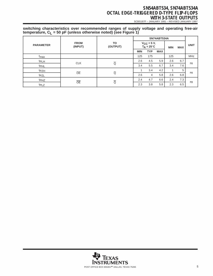
switching characteristics over recommended ranges of supply voltage and operating free-airtemperature, C L = 50 pF (unless otherwise noted) (see Figure 1)
SN74ABT534A
PARAMETERFROM
(INPUT)TO
(OUTPUT)VCC = 5 V,TA = 25°C MIN MAX
UNIT
MIN TYP MAX
fmax 125 175 125 MHz
tPLHCLK Q
2.6 4.5 5.9 2.6 6.7ns
tPHLCLK Q
3.4 5.5 6.7 3.4 7.6ns
tPZHOE Q
1 3.4 4.2 1 5ns
tPZLOE Q
2.6 4 5.8 2.6 6.8ns
tPHZOE Q
2.4 4.7 6.6 2.4 7.3ns
tPLZOE Q
2.3 3.8 5.8 2.3 6.5ns
SN54ABT534, SN74ABT534AOCTAL EDGE-TRIGGERED D-TYPE FLIP-FLOPSWITH 3-STATE OUTPUTS
SCBS187F – JANUARY 1991 – REVISED JANUARY 1997
6 POST OFFICE BOX 655303 • DALLAS, TEXAS 75265
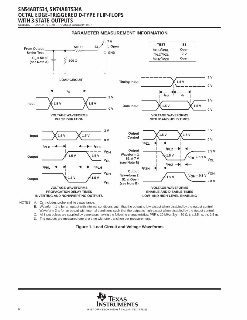
PARAMETER MEASUREMENT INFORMATION
1.5 V
thtsu
From Output Under Test
CL = 50 pF(see Note A)
LOAD CIRCUIT
S1
7 V
Open
GND
500 Ω
500 Ω
Data Input
Timing Input 1.5 V3 V
0 V
1.5 V 1.5 V
3 V
0 V
3 V
0 V
1.5 V
tw
Input
VOLTAGE WAVEFORMSSETUP AND HOLD TIMES
VOLTAGE WAVEFORMSPROPAGATION DELAY TIMES
INVERTING AND NONINVERTING OUTPUTS
VOLTAGE WAVEFORMSPULSE DURATION
tPLH
tPHL
tPHL
tPLH
VOH
VOH
VOL
VOL
1.5 V 1.5 V
3 V
0 V
1.5 V1.5 V
Input
1.5 V
OutputControl
OutputWaveform 1
S1 at 7 V(see Note B)
OutputWaveform 2S1 at Open
(see Note B)
VOL
VOH
tPZL
tPZH
tPLZ
tPHZ
1.5 V1.5 V
3.5 V
0 V
1.5 V VOL + 0.3 V
1.5 V VOH – 0.3 V
≈ 0 V
3 V
VOLTAGE WAVEFORMSENABLE AND DISABLE TIMES
LOW- AND HIGH-LEVEL ENABLING
Output
Output
tPLH/tPHLtPLZ/tPZLtPHZ/tPZH
Open7 V
Open
TEST S1
OutputControl
NOTES: A. CL includes probe and jig capacitance.B. Waveform 1 is for an output with internal conditions such that the output is low except when disabled by the output control.
Waveform 2 is for an output with internal conditions such that the output is high except when disabled by the output control.C. All input pulses are supplied by generators having the following characteristics: PRR ≤ 10 MHz, ZO = 50 Ω, tr ≤ 2.5 ns, tf ≤ 2.5 ns.D. The outputs are measured one at a time with one transition per measurement.
1.5 V
Figure 1. Load Circuit and Voltage Waveforms
PACKAGE OPTION ADDENDUM
www.ti.com 31-Oct-2021
Addendum-Page 1
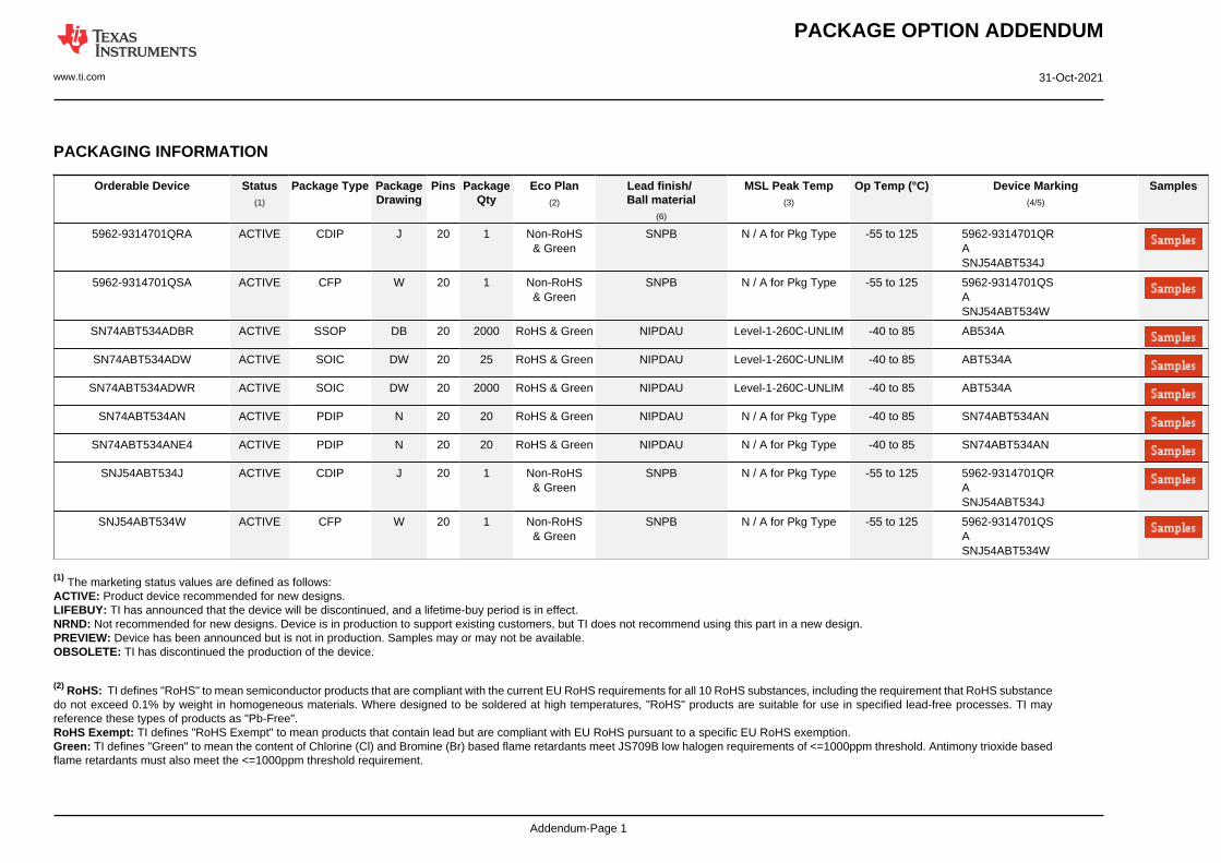
PACKAGING INFORMATION
Orderable Device Status(1)
Package Type PackageDrawing
Pins PackageQty
Eco Plan(2)
Lead finish/Ball material
(6)
MSL Peak Temp(3)
Op Temp (°C) Device Marking(4/5)
Samples
5962-9314701QRA ACTIVE CDIP J 20 1 Non-RoHS& Green
SNPB N / A for Pkg Type -55 to 125 5962-9314701QRASNJ54ABT534J
5962-9314701QSA ACTIVE CFP W 20 1 Non-RoHS& Green
SNPB N / A for Pkg Type -55 to 125 5962-9314701QSASNJ54ABT534W
SN74ABT534ADBR ACTIVE SSOP DB 20 2000 RoHS & Green NIPDAU Level-1-260C-UNLIM -40 to 85 AB534A
SN74ABT534ADW ACTIVE SOIC DW 20 25 RoHS & Green NIPDAU Level-1-260C-UNLIM -40 to 85 ABT534A
SN74ABT534ADWR ACTIVE SOIC DW 20 2000 RoHS & Green NIPDAU Level-1-260C-UNLIM -40 to 85 ABT534A
SN74ABT534AN ACTIVE PDIP N 20 20 RoHS & Green NIPDAU N / A for Pkg Type -40 to 85 SN74ABT534AN
SN74ABT534ANE4 ACTIVE PDIP N 20 20 RoHS & Green NIPDAU N / A for Pkg Type -40 to 85 SN74ABT534AN
SNJ54ABT534J ACTIVE CDIP J 20 1 Non-RoHS& Green
SNPB N / A for Pkg Type -55 to 125 5962-9314701QRASNJ54ABT534J
SNJ54ABT534W ACTIVE CFP W 20 1 Non-RoHS& Green
SNPB N / A for Pkg Type -55 to 125 5962-9314701QSASNJ54ABT534W
(1) The marketing status values are defined as follows:ACTIVE: Product device recommended for new designs.LIFEBUY: TI has announced that the device will be discontinued, and a lifetime-buy period is in effect.NRND: Not recommended for new designs. Device is in production to support existing customers, but TI does not recommend using this part in a new design.PREVIEW: Device has been announced but is not in production. Samples may or may not be available.OBSOLETE: TI has discontinued the production of the device.
(2) RoHS: TI defines "RoHS" to mean semiconductor products that are compliant with the current EU RoHS requirements for all 10 RoHS substances, including the requirement that RoHS substancedo not exceed 0.1% by weight in homogeneous materials. Where designed to be soldered at high temperatures, "RoHS" products are suitable for use in specified lead-free processes. TI mayreference these types of products as "Pb-Free".RoHS Exempt: TI defines "RoHS Exempt" to mean products that contain lead but are compliant with EU RoHS pursuant to a specific EU RoHS exemption.Green: TI defines "Green" to mean the content of Chlorine (Cl) and Bromine (Br) based flame retardants meet JS709B low halogen requirements of <=1000ppm threshold. Antimony trioxide basedflame retardants must also meet the <=1000ppm threshold requirement.
PACKAGE OPTION ADDENDUM
www.ti.com 31-Oct-2021
Addendum-Page 2
(3) MSL, Peak Temp. - The Moisture Sensitivity Level rating according to the JEDEC industry standard classifications, and peak solder temperature.
(4) There may be additional marking, which relates to the logo, the lot trace code information, or the environmental category on the device.
(5) Multiple Device Markings will be inside parentheses. Only one Device Marking contained in parentheses and separated by a "~" will appear on a device. If a line is indented then it is a continuationof the previous line and the two combined represent the entire Device Marking for that device.
(6) Lead finish/Ball material - Orderable Devices may have multiple material finish options. Finish options are separated by a vertical ruled line. Lead finish/Ball material values may wrap to twolines if the finish value exceeds the maximum column width.
Important Information and Disclaimer:The information provided on this page represents TI's knowledge and belief as of the date that it is provided. TI bases its knowledge and belief on informationprovided by third parties, and makes no representation or warranty as to the accuracy of such information. Efforts are underway to better integrate information from third parties. TI has taken andcontinues to take reasonable steps to provide representative and accurate information but may not have conducted destructive testing or chemical analysis on incoming materials and chemicals.TI and TI suppliers consider certain information to be proprietary, and thus CAS numbers and other limited information may not be available for release.
In no event shall TI's liability arising out of such information exceed the total purchase price of the TI part(s) at issue in this document sold by TI to Customer on an annual basis.
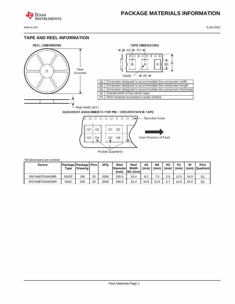
TAPE AND REEL INFORMATION
*All dimensions are nominal
Device PackageType
PackageDrawing
Pins SPQ ReelDiameter
(mm)
ReelWidth
W1 (mm)
A0(mm)
B0(mm)
K0(mm)
P1(mm)
W(mm)
Pin1Quadrant
SN74ABT534ADBR SSOP DB 20 2000 330.0 16.4 8.2 7.5 2.5 12.0 16.0 Q1
SN74ABT534ADWR SOIC DW 20 2000 330.0 24.4 10.8 13.3 2.7 12.0 24.0 Q1
PACKAGE MATERIALS INFORMATION
www.ti.com 5-Jan-2022
Pack Materials-Page 1
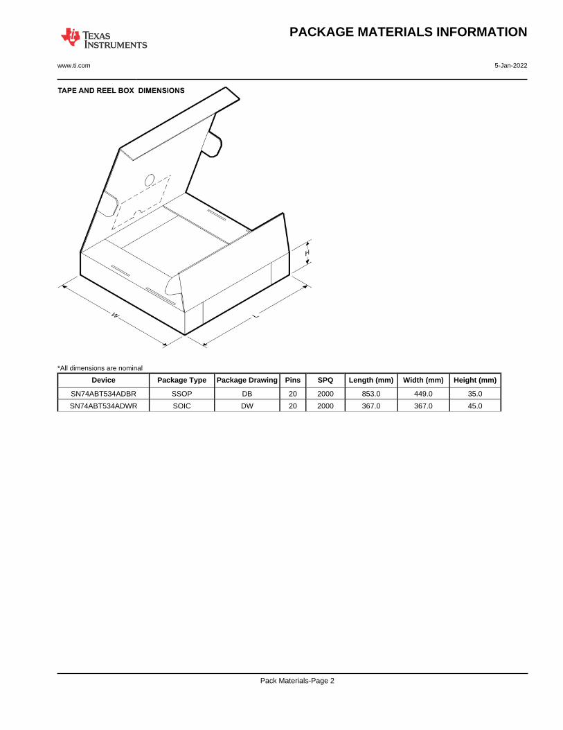
*All dimensions are nominal
Device Package Type Package Drawing Pins SPQ Length (mm) Width (mm) Height (mm)
SN74ABT534ADBR SSOP DB 20 2000 853.0 449.0 35.0
SN74ABT534ADWR SOIC DW 20 2000 367.0 367.0 45.0
PACKAGE MATERIALS INFORMATION
www.ti.com 5-Jan-2022
Pack Materials-Page 2
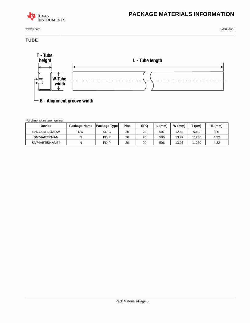
TUBE
*All dimensions are nominal
Device Package Name Package Type Pins SPQ L (mm) W (mm) T (µm) B (mm)
SN74ABT534ADW DW SOIC 20 25 507 12.83 5080 6.6
SN74ABT534AN N PDIP 20 20 506 13.97 11230 4.32
SN74ABT534ANE4 N PDIP 20 20 506 13.97 11230 4.32
PACKAGE MATERIALS INFORMATION
www.ti.com 5-Jan-2022
Pack Materials-Page 3
www.ti.com
PACKAGE OUTLINE
C
18X 0.65
2X5.85
20X 0.380.22
8.27.4 TYP
SEATINGPLANE
0.05 MIN
0.25GAGE PLANE
0 -8
2 MAX
B 5.65.0
NOTE 4
A
7.56.9
NOTE 3
0.950.55
(0.15) TYP
SSOP - 2 mm max heightDB0020ASMALL OUTLINE PACKAGE
4214851/B 08/2019
1
1011
20
0.1 C A B
PIN 1 INDEX AREA
SEE DETAIL A
0.1 C
NOTES: 1. All linear dimensions are in millimeters. Any dimensions in parenthesis are for reference only. Dimensioning and tolerancing per ASME Y14.5M. 2. This drawing is subject to change without notice. 3. This dimension does not include mold flash, protrusions, or gate burrs. Mold flash, protrusions, or gate burrs shall not exceed 0.15 mm per side. 4. This dimension does not include interlead flash. Interlead flash shall not exceed 0.25 mm per side.5. Reference JEDEC registration MO-150.
A 15DETAIL ATYPICAL
SCALE 2.000
www.ti.com
EXAMPLE BOARD LAYOUT
0.07 MAXALL AROUND
0.07 MINALL AROUND
20X (1.85)
20X (0.45)
18X (0.65)
(7)
(R0.05) TYP
SSOP - 2 mm max heightDB0020ASMALL OUTLINE PACKAGE
4214851/B 08/2019
NOTES: (continued) 6. Publication IPC-7351 may have alternate designs. 7. Solder mask tolerances between and around signal pads can vary based on board fabrication site.
LAND PATTERN EXAMPLEEXPOSED METAL SHOWN
SCALE: 10X
SYMM
SYMM
1
10 11
20
15.000
METALSOLDER MASKOPENING
METAL UNDERSOLDER MASK
SOLDER MASKOPENING
EXPOSED METALEXPOSED METAL
SOLDER MASK DETAILS
NON-SOLDER MASKDEFINED
(PREFERRED)
SOLDER MASKDEFINED
www.ti.com
EXAMPLE STENCIL DESIGN
20X (1.85)
20X (0.45)
18X (0.65)
(7)
(R0.05) TYP
SSOP - 2 mm max heightDB0020ASMALL OUTLINE PACKAGE
4214851/B 08/2019
NOTES: (continued) 8. Laser cutting apertures with trapezoidal walls and rounded corners may offer better paste release. IPC-7525 may have alternate design recommendations. 9. Board assembly site may have different recommendations for stencil design.
SOLDER PASTE EXAMPLEBASED ON 0.125 mm THICK STENCIL
SCALE: 10X
SYMM
SYMM
1
10 11
20

www.ti.com
PACKAGE OUTLINE
C
TYP10.639.97
2.65 MAX
18X 1.27
20X 0.510.31
2X11.43
TYP0.330.10
0 - 80.30.1
0.25GAGE PLANE
1.270.40
A
NOTE 3
13.012.6
B 7.67.4
4220724/A 05/2016
SOIC - 2.65 mm max heightDW0020ASOIC
NOTES: 1. All linear dimensions are in millimeters. Dimensions in parenthesis are for reference only. Dimensioning and tolerancing per ASME Y14.5M. 2. This drawing is subject to change without notice. 3. This dimension does not include mold flash, protrusions, or gate burrs. Mold flash, protrusions, or gate burrs shall not exceed 0.15 mm per side. 4. This dimension does not include interlead flash. Interlead flash shall not exceed 0.43 mm per side.5. Reference JEDEC registration MS-013.
120
0.25 C A B
1110
PIN 1 IDAREA
NOTE 4
SEATING PLANE
0.1 C
SEE DETAIL A
DETAIL ATYPICAL
SCALE 1.200
www.ti.com
EXAMPLE BOARD LAYOUT
(9.3)
0.07 MAXALL AROUND
0.07 MINALL AROUND
20X (2)
20X (0.6)
18X (1.27)
(R )TYP
0.05
4220724/A 05/2016
SOIC - 2.65 mm max heightDW0020ASOIC
SYMM
SYMM
LAND PATTERN EXAMPLESCALE:6X
1
10 11
20
NOTES: (continued) 6. Publication IPC-7351 may have alternate designs. 7. Solder mask tolerances between and around signal pads can vary based on board fabrication site.
METALSOLDER MASKOPENING
NON SOLDER MASKDEFINED
SOLDER MASK DETAILS
SOLDER MASKOPENING
METAL UNDERSOLDER MASK
SOLDER MASKDEFINED
www.ti.com
EXAMPLE STENCIL DESIGN
(9.3)
18X (1.27)
20X (0.6)
20X (2)
4220724/A 05/2016
SOIC - 2.65 mm max heightDW0020ASOIC
NOTES: (continued) 8. Laser cutting apertures with trapezoidal walls and rounded corners may offer better paste release. IPC-7525 may have alternate design recommendations. 9. Board assembly site may have different recommendations for stencil design.
SYMM
SYMM
1
10 11
20
SOLDER PASTE EXAMPLEBASED ON 0.125 mm THICK STENCIL
SCALE:6X
IMPORTANT NOTICE AND DISCLAIMERTI PROVIDES TECHNICAL AND RELIABILITY DATA (INCLUDING DATA SHEETS), DESIGN RESOURCES (INCLUDING REFERENCE DESIGNS), APPLICATION OR OTHER DESIGN ADVICE, WEB TOOLS, SAFETY INFORMATION, AND OTHER RESOURCES “AS IS” AND WITH ALL FAULTS, AND DISCLAIMS ALL WARRANTIES, EXPRESS AND IMPLIED, INCLUDING WITHOUT LIMITATION ANY IMPLIED WARRANTIES OF MERCHANTABILITY, FITNESS FOR A PARTICULAR PURPOSE OR NON-INFRINGEMENT OF THIRD PARTY INTELLECTUAL PROPERTY RIGHTS.These resources are intended for skilled developers designing with TI products. You are solely responsible for (1) selecting the appropriate TI products for your application, (2) designing, validating and testing your application, and (3) ensuring your application meets applicable standards, and any other safety, security, regulatory or other requirements.These resources are subject to change without notice. TI grants you permission to use these resources only for development of an application that uses the TI products described in the resource. Other reproduction and display of these resources is prohibited. No license is granted to any other TI intellectual property right or to any third party intellectual property right. TI disclaims responsibility for, and you will fully indemnify TI and its representatives against, any claims, damages, costs, losses, and liabilities arising out of your use of these resources.TI’s products are provided subject to TI’s Terms of Sale or other applicable terms available either on ti.com or provided in conjunction with such TI products. TI’s provision of these resources does not expand or otherwise alter TI’s applicable warranties or warranty disclaimers for TI products.TI objects to and rejects any additional or different terms you may have proposed. IMPORTANT NOTICE
Mailing Address: Texas Instruments, Post Office Box 655303, Dallas, Texas 75265Copyright © 2022, Texas Instruments Incorporated