Nulling Input Offset Voltage of Operational · PDF fileSLOA045 Nulling Input Offset Voltage of...
15
Application Report SLOA045 - August 2000 1 Nulling Input Offset Voltage of Operational Amplifiers Bao Nguyen and W. David Smith Mixed Signal Products ABSTRACT The input offset voltage of operational amplifiers (op amps) arises from unavoidable mismatches in the differential input stage of the op-amp circuit caused by mismatched transistor pairs, collector currents, current-gain betas(β), collector or emitter resistors, etc. This application report describes the effects of mismatched components on the input offset voltage, and proposes using an external null circuit to reduce the input offset voltage of an amplifier. It also suggests a means for computing proper values of resistors in the null circuit in order to provide appropriate input-offset-voltage compensation. Contents 1 Introduction 2 . . . . . . . . . . . . . . . . . . . . . . . . . . . . . . . . . . . . . . . . . . . . . . . . . . . . . . . . . . . . . . . . . . . . . . . . . 2 Effect of Component Mismatches in the Input Offset Voltage 2 . . . . . . . . . . . . . . . . . . . . . . . . . . . . 2.1 Effect of Collector-Resistor (R c ) Mismatch on V os 3 . . . . . . . . . . . . . . . . . . . . . . . . . . . . . . . . . . . . . 2.2 Effect of Mismatched Transistors on V os 4 . . . . . . . . . . . . . . . . . . . . . . . . . . . . . . . . . . . . . . . . . . . . . 3 External Null Circuit 6 . . . . . . . . . . . . . . . . . . . . . . . . . . . . . . . . . . . . . . . . . . . . . . . . . . . . . . . . . . . . . . . . . . 3.1 Effect of the Potentiometer on Vos 6 . . . . . . . . . . . . . . . . . . . . . . . . . . . . . . . . . . . . . . . . . . . . . . . . . . 3.1.1 TLC070 7 . . . . . . . . . . . . . . . . . . . . . . . . . . . . . . . . . . . . . . . . . . . . . . . . . . . . . . . . . . . . . . . . . . . 3.1.2 THS4011 7 . . . . . . . . . . . . . . . . . . . . . . . . . . . . . . . . . . . . . . . . . . . . . . . . . . . . . . . . . . . . . . . . . 3.2 Effect of Additional Temperature-Coefficient Resistors on V os 8 . . . . . . . . . . . . . . . . . . . . . . . . . . 3.2.1 Low Temperature-Coefficient Resistor 8 . . . . . . . . . . . . . . . . . . . . . . . . . . . . . . . . . . . . . . . . 3.2.2 Effect of High Temperature-Coefficient Resistor (Thermistor) on V os 9 . . . . . . . . . . . . . . 3.2.3 TLC070 10 . . . . . . . . . . . . . . . . . . . . . . . . . . . . . . . . . . . . . . . . . . . . . . . . . . . . . . . . . . . . . . . . . . 3.2.4 THS4011 11 . . . . . . . . . . . . . . . . . . . . . . . . . . . . . . . . . . . . . . . . . . . . . . . . . . . . . . . . . . . . . . . . 4 Summary 13 . . . . . . . . . . . . . . . . . . . . . . . . . . . . . . . . . . . . . . . . . . . . . . . . . . . . . . . . . . . . . . . . . . . . . . . . . . . 5 References 14 . . . . . . . . . . . . . . . . . . . . . . . . . . . . . . . . . . . . . . . . . . . . . . . . . . . . . . . . . . . . . . . . . . . . . . . . . List of Figures 1 The Simplified Differential Input Circuit 2 . . . . . . . . . . . . . . . . . . . . . . . . . . . . . . . . . . . . . . . . . . . . . . . . . . . . . 2 The Simplified Differential Input Circuit With MOSFET 5 . . . . . . . . . . . . . . . . . . . . . . . . . . . . . . . . . . . . . . . 3 The Null Pins Connected to the Op Amp 6 . . . . . . . . . . . . . . . . . . . . . . . . . . . . . . . . . . . . . . . . . . . . . . . . . . . 4 The Potentiometer in the Null Circuit 7 . . . . . . . . . . . . . . . . . . . . . . . . . . . . . . . . . . . . . . . . . . . . . . . . . . . . . . . 5V os of TLC070 With the Potentiometer in the Null Circuit 7 . . . . . . . . . . . . . . . . . . . . . . . . . . . . . . . . . . . . . 6V os of TLC4011 With the Potentiometer in the Null Circuit 8 . . . . . . . . . . . . . . . . . . . . . . . . . . . . . . . . . . . . 7 The Null Circuit of the Potentiometer in Series With a Resistor 8 . . . . . . . . . . . . . . . . . . . . . . . . . . . . . . . . 8V os Variation of TLC070 With the Low Temperature-Coefficient Resistors in the Null Circuit 9 . . . . . . . 9 Temperature Dependence of Resistance for Five Thermistors 9 . . . . . . . . . . . . . . . . . . . . . . . . . . . . . . . . .
-
Upload
duongkhanh -
Category
Documents
-
view
217 -
download
3
Transcript of Nulling Input Offset Voltage of Operational · PDF fileSLOA045 Nulling Input Offset Voltage of...
Application ReportSLOA045 - August 2000
1
Nulling Input Offset Voltage of Operational AmplifiersBao Nguyen and W. David Smith Mixed Signal Products
ABSTRACT
The input offset voltage of operational amplifiers (op amps) arises from unavoidablemismatches in the differential input stage of the op-amp circuit caused by mismatchedtransistor pairs, collector currents, current-gain betas(β), collector or emitter resistors, etc.This application report describes the effects of mismatched components on the input offsetvoltage, and proposes using an external null circuit to reduce the input offset voltage of anamplifier. It also suggests a means for computing proper values of resistors in the null circuitin order to provide appropriate input-offset-voltage compensation.
Contents
1 Introduction 2. . . . . . . . . . . . . . . . . . . . . . . . . . . . . . . . . . . . . . . . . . . . . . . . . . . . . . . . . . . . . . . . . . . . . . . . .
2 Effect of Component Mismatches in the Input Offset Voltage 2. . . . . . . . . . . . . . . . . . . . . . . . . . . . 2.1 Effect of Collector-Resistor (Rc) Mismatch on Vos 3. . . . . . . . . . . . . . . . . . . . . . . . . . . . . . . . . . . . . 2.2 Effect of Mismatched Transistors on Vos 4. . . . . . . . . . . . . . . . . . . . . . . . . . . . . . . . . . . . . . . . . . . . .
3 External Null Circuit 6. . . . . . . . . . . . . . . . . . . . . . . . . . . . . . . . . . . . . . . . . . . . . . . . . . . . . . . . . . . . . . . . . . 3.1 Effect of the Potentiometer on Vos 6. . . . . . . . . . . . . . . . . . . . . . . . . . . . . . . . . . . . . . . . . . . . . . . . . .
3.1.1 TLC070 7. . . . . . . . . . . . . . . . . . . . . . . . . . . . . . . . . . . . . . . . . . . . . . . . . . . . . . . . . . . . . . . . . . . 3.1.2 THS4011 7. . . . . . . . . . . . . . . . . . . . . . . . . . . . . . . . . . . . . . . . . . . . . . . . . . . . . . . . . . . . . . . . .
3.2 Effect of Additional Temperature-Coefficient Resistors on Vos 8. . . . . . . . . . . . . . . . . . . . . . . . . . 3.2.1 Low Temperature-Coefficient Resistor 8. . . . . . . . . . . . . . . . . . . . . . . . . . . . . . . . . . . . . . . . 3.2.2 Effect of High Temperature-Coefficient Resistor (Thermistor) on Vos 9. . . . . . . . . . . . . . 3.2.3 TLC070 10. . . . . . . . . . . . . . . . . . . . . . . . . . . . . . . . . . . . . . . . . . . . . . . . . . . . . . . . . . . . . . . . . . 3.2.4 THS4011 11. . . . . . . . . . . . . . . . . . . . . . . . . . . . . . . . . . . . . . . . . . . . . . . . . . . . . . . . . . . . . . . .
4 Summary 13. . . . . . . . . . . . . . . . . . . . . . . . . . . . . . . . . . . . . . . . . . . . . . . . . . . . . . . . . . . . . . . . . . . . . . . . . . .
5 References 14. . . . . . . . . . . . . . . . . . . . . . . . . . . . . . . . . . . . . . . . . . . . . . . . . . . . . . . . . . . . . . . . . . . . . . . . .
List of Figures
1 The Simplified Differential Input Circuit 2. . . . . . . . . . . . . . . . . . . . . . . . . . . . . . . . . . . . . . . . . . . . . . . . . . . . . 2 The Simplified Differential Input Circuit With MOSFET 5. . . . . . . . . . . . . . . . . . . . . . . . . . . . . . . . . . . . . . . 3 The Null Pins Connected to the Op Amp 6. . . . . . . . . . . . . . . . . . . . . . . . . . . . . . . . . . . . . . . . . . . . . . . . . . . 4 The Potentiometer in the Null Circuit 7. . . . . . . . . . . . . . . . . . . . . . . . . . . . . . . . . . . . . . . . . . . . . . . . . . . . . . . 5 Vos of TLC070 With the Potentiometer in the Null Circuit 7. . . . . . . . . . . . . . . . . . . . . . . . . . . . . . . . . . . . . 6 Vos of TLC4011 With the Potentiometer in the Null Circuit 8. . . . . . . . . . . . . . . . . . . . . . . . . . . . . . . . . . . . 7 The Null Circuit of the Potentiometer in Series With a Resistor 8. . . . . . . . . . . . . . . . . . . . . . . . . . . . . . . . 8 Vos Variation of TLC070 With the Low Temperature-Coefficient Resistors in the Null Circuit 9. . . . . . . 9 Temperature Dependence of Resistance for Five Thermistors 9. . . . . . . . . . . . . . . . . . . . . . . . . . . . . . . . .
SLOA045
2 Nulling Input Offset Voltage of Operational Amplifiers
10 The Null Circuit With the Potentiometer in Series With Parallel Resistors 10. . . . . . . . . . . . . . . . . . . . . 11 Vos With Req = 6 kΩ//10 kΩ in Series With the Potentiometer in the Null Circuit 11. . . . . . . . . . . . . . . 12 Vos With Req = 1 kΩ//10 kΩ in Series With the Potentiometer in the Null Circuit 12. . . . . . . . . . . . . . . 13 Vos With Req = 20 kΩ//2.2 kΩ in Series With the Potentiometer in the Null Circuit 13. . . . . . . . . . . . .
List of Tables
1 Values of the Resistors in the Null Circuit of Figure 10 10. . . . . . . . . . . . . . . . . . . . . . . . . . . . . . . . . . . . . . 2 Values of Resistors in the Null Circuit of Figure 10 for the First Attempt 11. . . . . . . . . . . . . . . . . . . . . . . . 3 Values of Resistors in the Null Circuit of Figure 10 for the Second Attempt 12. . . . . . . . . . . . . . . . . . . . . 4 Summary of Vos Results for TLC070 and THS4011 With Various Null Circuits. 14. . . . . . . . . . . . . . . . .
1 Introduction
Operational amplifiers (op amps) may exhibit an input offset voltage (Vos) in the range of µV tomV. Since the active and passive devices in the internal op-amp circuit have inherenttemperature-dependent parameters, so does the input offset voltage. The op-amp data sheetsusually specify the typical and maximum values, as well as the temperature coefficient of theinput offset voltage. However, the data sheets do not present the polarity of Vos because thechange in the input offset voltage caused by component mismatches is unknown.
The op-amp data sheets usually recommend the use of an external potentiometer connected tothe null pins to zero Vos at room temperature; this method is first shown in detail. In addition, analternative approach is also presented that minimizes the input-offset-voltage range overtemperature by adding a resistor with a known temperature coefficient (Ω/°C) to the null circuit.This resistor is connected to either side of the null pins, depending on the polarity of Vos, andserves to balance the voltages at the input terminals of an op amp.
2 Effect of Component Mismatches in the Input Offset Voltage
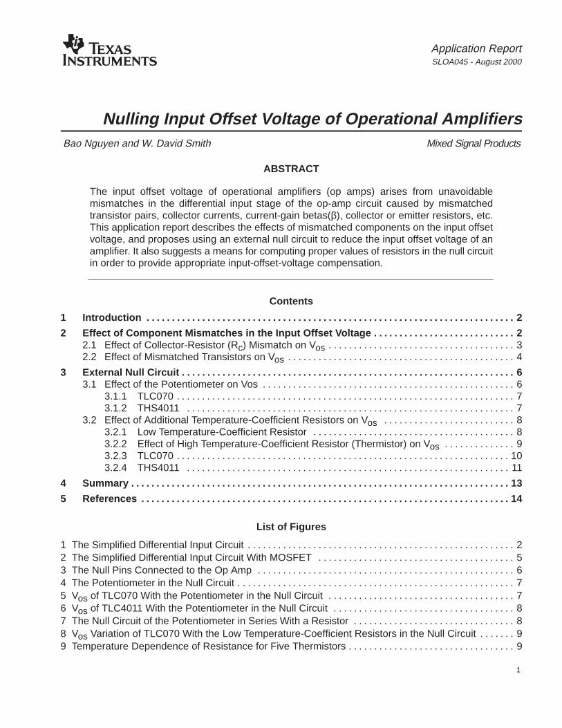
Consider the simplified input-stage circuit of the operational amplifier in Figure 1. The inputoffset voltage of the op amp results from mismatches in collector/emitter resistors and thetransistor pair of the differential input. Each of these mismatches is examined separately below.
Q1 Q2
VC2
RC2RC1
I
+
–
VOS
VDD
VI(–)VI(+)
VC1
Figure 1. The Simplified Differential Input Circuit
SLOA045
3 Nulling Input Offset Voltage of Operational Amplifiers
2.1 Effect of Collector-Resistor (R c) Mismatch on V os
When the transistors Q1 and Q2 in Figure 1 are perfectly matched, the current, I, is dividedequally between them.
Let Rc Rc1 Rc2
2and Rc Rc1 Rc2
Then, Rc1 Rc Rc
2and Rc2 Rc
Rc2
Thus, the output voltage, Vo, is [1a]:
Vo Vc2 Vc1 VDD αI2
Rc2 VDD αI
2Rc1 VDD αI
2Rc
Rc2
VDD αI2Rc
Rc2 Rc
αI2
The input offset voltage is Vos VoAd
Vo
gmRc
αRc I
2
αI2
VTRc
VTRcRc
kTq
RcRc
(1)
α
1; differential gain : Ad gmRc; gm
IcVT
and VT kTq is the thermal voltage.
where
Here k is Boltzmann’s constant and q is the charge on the electron
SLOA045
4 Nulling Input Offset Voltage of Operational Amplifiers
2.2 Effect of Mismatched Transistors on V os
Mismatch in transistors usually occurs because of mismatches in emitter areas for bipolarjunction transistors (BJT) and W/L ratios for MOSFETs. Since either BJT or MOSFET transistorscan be used in the differential input stage, each is analyzed separately below.
Mismatched emitter-base junction areas of BJTs give mismatches in current saturation junctionIS.
Let Is Is1 Is2
2and Is Is1 Is2
Then, Is1 Is Is2
Is1 Is2Is and Is2 Is–
Is2
Is1–Is2Is
Assume that the voltages across base-emitter junctions are equal(VBE1 = VBE2); then
Ic1 Is1eVBE1
VT
IseVBE1
VT 1
Is2Is αI
21
Is2Is Ic1
Is2Is
Ic2 Is2eVBE2
VT
IseVBE2
VT 1
Is2Is αI
21
Is2Is Ic1
Is2Is
Assume Rc1 and Rc2 are perfectly matched (Rc1 = Rc2). Thus, the output voltage Vo is:[1b]
Vo Vc2 Vc1 VDD Ic2Rc2 VDD Ic1Rc1
Ic1–Ic2Rc
RcαI21
Is2Is–1–
Is2Is αI
2IsIs
Rc
Vos VoAd
Vo
gmRc
αI2
IsIs
Rc
αI2
VT
VTIsIs
kTq
IsIs
(2)
Rc
SLOA045
5 Nulling Input Offset Voltage of Operational Amplifiers
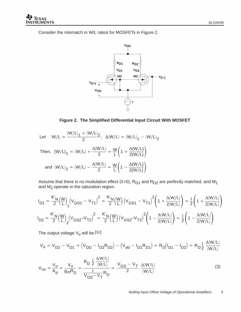
Consider the mismatch in W/L ratios for MOSFETs in Figure 2.
I
V(I–)
VD2VD1
M2M2
RD2RD1
+
–
V(I+)
VOS
VDD
Figure 2. The Simplified Differential Input Circuit With MOSFET
Let WL WL1 WL2
2; WL WL1 WL2
Then, (WL)1 WL WL
2 W
L1
(WL)2(WL)
and WL2 WL WL
2 W
L1
(WL)2(WL)
Assume that there is no modulation effect (λ=0), RD1 and RD2 are perfectly matched, and M1and M2 operate in the saturation region.
ID1 K′N2W
L
1VGS1 VT1
2 K′N2W
L VGS1 VT1
21 WL
2WL I
21
WL
2WL
ID2 K′N2W
L
2VGS2–VT2
2 K′N2W
L VGS2–VT2
21 WL
2WL I
21
WL
2WL
The output voltage Vo will be:[1c]
Vo VD2 VD1 VDD ID2RD2 Vdd ID1RD1
RDID1 ID2
RDI2
WL
WL
Vos VoAd
Vo
gmRD
RDI2
WLWL
IVGSVT
RD
VGS VT
2WL
WL(3)
SLOA045
6 Nulling Input Offset Voltage of Operational Amplifiers
where VGS is the gate-source voltage, and the threshold voltage VT is dependent ontemperature since [2]
VT VTO 2F VBS 2F
where VTO kTq ln
NGNBn2
i
QoxCox
2F QDCox
For all three of these cases, the input offset voltage of the amplifier mostly has contributionsfrom the mismatches in those components as shown in Equations 1, 2, and 3. In addition, theVos is obviously dependent on temperature through the parameter VT of the transistors.
3 External Null Circuit
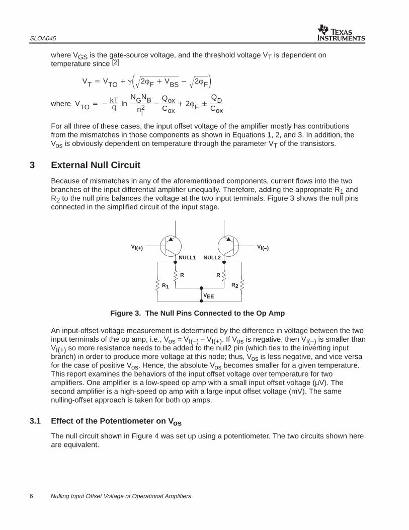
Because of mismatches in any of the aforementioned components, current flows into the twobranches of the input differential amplifier unequally. Therefore, adding the appropriate R1 andR2 to the null pins balances the voltage at the two input terminals. Figure 3 shows the null pinsconnected in the simplified circuit of the input stage.
VEE
NULL1 NULL2
R
VI(–)VI(+)
R
R1 R2
Figure 3. The Null Pins Connected to the Op Amp
An input-offset-voltage measurement is determined by the difference in voltage between the twoinput terminals of the op amp, i.e., Vos = VI(–) – VI(+). If Vos is negative, then VI(–) is smaller thanVI(+) so more resistance needs to be added to the null2 pin (which ties to the inverting inputbranch) in order to produce more voltage at this node; thus, Vos is less negative, and vice versafor the case of positive Vos. Hence, the absolute Vos becomes smaller for a given temperature.This report examines the behaviors of the input offset voltage over temperature for twoamplifiers. One amplifier is a low-speed op amp with a small input offset voltage (µV). Thesecond amplifier is a high-speed op amp with a large input offset voltage (mV). The samenulling-offset approach is taken for both op amps.
3.1 Effect of the Potentiometer on V os
The null circuit shown in Figure 4 was set up using a potentiometer. The two circuits shown hereare equivalent.
SLOA045
7 Nulling Input Offset Voltage of Operational Amplifiers
VEE/GND
NULL1 NULL2
Rp1 Rp2
VEE (Split Supply)
GND (Single Supply)
Pot
VI(–)
VI(+)
OUT
VEE/GND
Figure 4. The Potentiometer in the Null Circuit
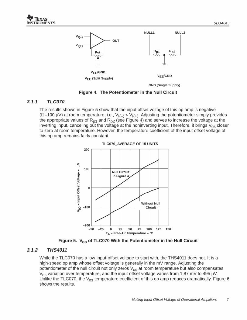
3.1.1 TLC070
The results shown in Figure 5 show that the input offset voltage of this op amp is negative (≅ –100 µV) at room temperature, i.e., VI(–) < VI(+). Adjusting the potentiometer simply providesthe appropriate values of Rp1 and Rp2 (see Figure 4) and serves to increase the voltage at theinverting input, canceling out the voltage at the noninverting input. Therefore, it brings Vos closerto zero at room temperature. However, the temperature coefficient of the input offset voltage ofthis op amp remains fairly constant.
–200
–100
0
100
200
–50 –25 0 25 50 75 100 125 150
Without NullCircuit
Null Circuitin Figure 4
– In
put O
ffset
Vol
tage
–
TLC070_AVERAGE OF 15 UNITS
TA – Free-Air Temperature – °C
VIO
Vµ
Figure 5. V os of TLC070 With the Potentiometer in the Null Circuit
3.1.2 THS4011
While the TLC070 has a low-input-offset voltage to start with, the THS4011 does not. It is ahigh-speed op amp whose offset voltage is generally in the mV range. Adjusting thepotentiometer of the null circuit not only zeros Vos at room temperature but also compensatesVos variation over temperature, and the input offset voltage varies from 1.87 mV to 495 µV.Unlike the TLC070, the Vos temperature coefficient of this op amp reduces dramatically. Figure 6shows the results.
SLOA045
8 Nulling Input Offset Voltage of Operational Amplifiers
–5
–4
–3
–2
–1
0
1
–50 –25 0 25 50 75 100 125 150
Without Null Circuit
– In
put O
ffset
Vol
tage
– m
V
THS4011_AVERAGE OF 15 SAMPLES
TA – Free-Air Temperature – °C
VIO
Null Circuitin Figure 4
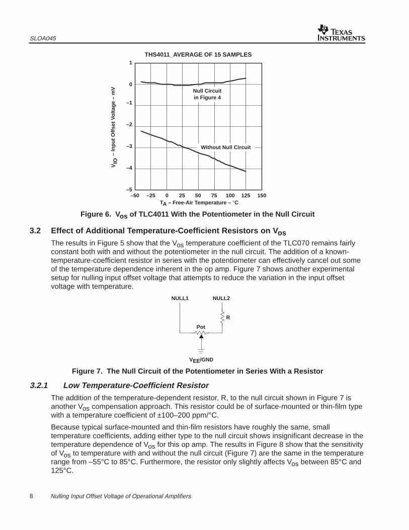
Figure 6. V os of TLC4011 With the Potentiometer in the Null Circuit
3.2 Effect of Additional Temperature-Coefficient Resistors on V osThe results in Figure 5 show that the Vos temperature coefficient of the TLC070 remains fairlyconstant both with and without the potentiometer in the null circuit. The addition of a known-temperature-coefficient resistor in series with the potentiometer can effectively cancel out someof the temperature dependence inherent in the op amp. Figure 7 shows another experimentalsetup for nulling input offset voltage that attempts to reduce the variation in the input offsetvoltage with temperature.
Pot
VEE/GND
R
NULL1 NULL2
Figure 7. The Null Circuit of the Potentiometer in Series With a Resistor
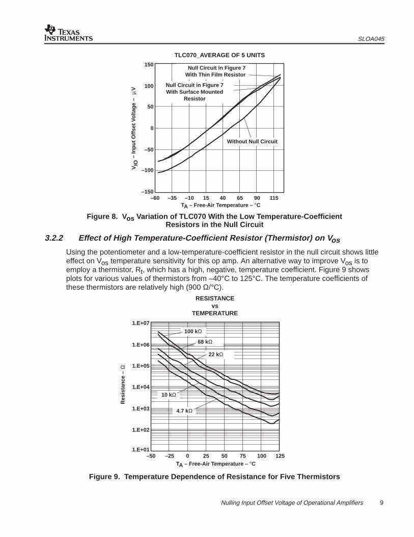
3.2.1 Low Temperature-Coefficient ResistorThe addition of the temperature-dependent resistor, R, to the null circuit shown in Figure 7 isanother Vos compensation approach. This resistor could be of surface-mounted or thin-film typewith a temperature coefficient of ±100–200 ppm/°C.
Because typical surface-mounted and thin-film resistors have roughly the same, smalltemperature coefficients, adding either type to the null circuit shows insignificant decrease in thetemperature dependence of Vos for this op amp. The results in Figure 8 show that the sensitivityof Vos to temperature with and without the null circuit (Figure 7) are the same in the temperaturerange from –55°C to 85°C. Furthermore, the resistor only slightly affects Vos between 85°C and125°C.
SLOA045
9 Nulling Input Offset Voltage of Operational Amplifiers
–150
–100
–50
0
50
100
150
–60 –35 –10 15 40 65 90 115
– In
put O
ffset
Vol
tage
–
TLC070_AVERAGE OF 5 UNITS
TA – Free-Air Temperature – °C
VIO
Vµ
Without Null Circuit
Null Circuit in Figure 7With Surface Mounted
Resistor
Null Circuit in Figure 7With Thin Film Resistor
Figure 8. V os Variation of TLC070 With the Low Temperature-CoefficientResistors in the Null Circuit
3.2.2 Effect of High Temperature-Coefficient Resistor (Thermistor) on V os
Using the potentiometer and a low-temperature-coefficient resistor in the null circuit shows littleeffect on Vos temperature sensitivity for this op amp. An alternative way to improve Vos is toemploy a thermistor, Rt, which has a high, negative, temperature coefficient. Figure 9 showsplots for various values of thermistors from –40°C to 125°C. The temperature coefficients ofthese thermistors are relatively high (900 Ω/°C).
1.E+01
1.E+02
1.E+03
1.E+04
1.E+05
1.E+06
1.E+07
–50 –25 0 25 50 75 100 125
100 kΩ
68 kΩ
22 kΩ
4.7 kΩ
10 kΩ
RESISTANCEvs
TEMPERATURE
Res
ista
nce
–
TA – Free-Air Temperature – °C
Ω
Figure 9. Temperature Dependence of Resistance for Five Thermistors
SLOA045
10 Nulling Input Offset Voltage of Operational Amplifiers
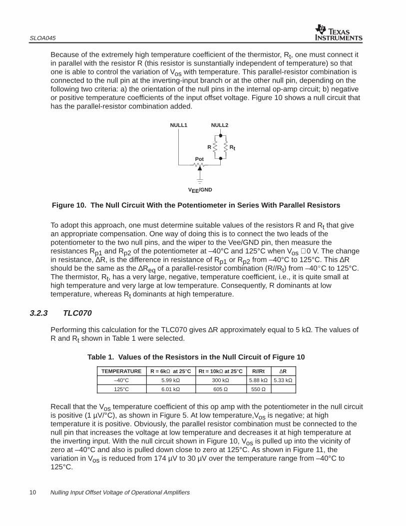
Because of the extremely high temperature coefficient of the thermistor, Rt, one must connect itin parallel with the resistor R (this resistor is sunstantially independent of temperature) so thatone is able to control the variation of Vos with temperature. This parallel-resistor combination isconnected to the null pin at the inverting-input branch or at the other null pin, depending on thefollowing two criteria: a) the orientation of the null pins in the internal op-amp circuit; b) negativeor positive temperature coefficients of the input offset voltage. Figure 10 shows a null circuit thathas the parallel-resistor combination added.
Pot
VEE/GND
Rt
NULL1 NULL2
R
Figure 10. The Null Circuit With the Potentiometer in Series With Parallel Resistors
To adopt this approach, one must determine suitable values of the resistors R and Rt that givean appropriate compensation. One way of doing this is to connect the two leads of thepotentiometer to the two null pins, and the wiper to the Vee/GND pin, then measure theresistances Rp1 and Rp2 of the potentiometer at –40°C and 125°C when Vos ≅ 0 V. The changein resistance, ∆R, is the difference in resistance of Rp1 or Rp2 from –40°C to 125°C. This ∆Rshould be the same as the ∆Req of a parallel-resistor combination (R//Rt) from –40C to 125°C.The thermistor, Rt, has a very large, negative, temperature coefficient, i.e., it is quite small athigh temperature and very large at low temperature. Consequently, R dominants at lowtemperature, whereas Rt dominants at high temperature.
3.2.3 TLC070
Performing this calculation for the TLC070 gives ∆R approximately equal to 5 kΩ. The values ofR and Rt shown in Table 1 were selected.
Table 1. Values of the Resistors in the Null Circuit of Figure 10
TEMPERATURE R = 6kΩ at 25°C Rt = 10kΩ at 25°C R//Rt ∆R
–40°C 5.99 kΩ 300 kΩ 5.88 kΩ 5.33 kΩ
125°C 6.01 kΩ 605 Ω 550 Ω
Recall that the Vos temperature coefficient of this op amp with the potentiometer in the null circuitis positive (1 µV/°C), as shown in Figure 5. At low temperature,Vos is negative; at hightemperature it is positive. Obviously, the parallel resistor combination must be connected to thenull pin that increases the voltage at low temperature and decreases it at high temperature atthe inverting input. With the null circuit shown in Figure 10, Vos is pulled up into the vicinity ofzero at –40°C and also is pulled down close to zero at 125°C. As shown in Figure 11, thevariation in Vos is reduced from 174 µV to 30 µV over the temperature range from –40°C to125°C.
SLOA045
11 Nulling Input Offset Voltage of Operational Amplifiers
–200
–100
0
100
200
–50 –25 0 25 50 75 100 125 150
– In
put O
ffset
Vol
tage
–
TLC070_AVERAGE OF 15 UNITS
TA – Free-Air Temperature – °C
VIO
Vµ Null Circuit in Figure 4
Without Null Circuit
Null Circuit in Figure 10
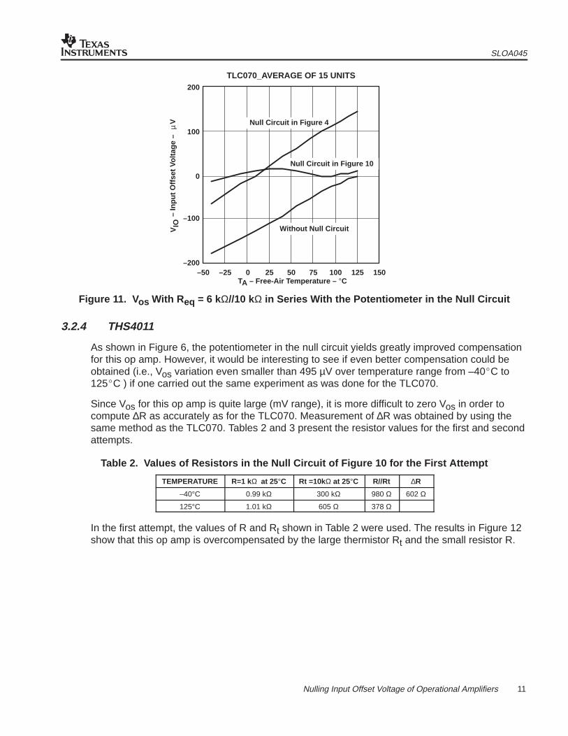
Figure 11. V os With R eq = 6 kΩ//10 kΩ in Series With the Potentiometer in the Null Circuit
3.2.4 THS4011
As shown in Figure 6, the potentiometer in the null circuit yields greatly improved compensationfor this op amp. However, it would be interesting to see if even better compensation could beobtained (i.e., Vos variation even smaller than 495 µV over temperature range from –40C to125C ) if one carried out the same experiment as was done for the TLC070.
Since Vos for this op amp is quite large (mV range), it is more difficult to zero Vos in order tocompute ∆R as accurately as for the TLC070. Measurement of ∆R was obtained by using thesame method as the TLC070. Tables 2 and 3 present the resistor values for the first and secondattempts.
Table 2. Values of Resistors in the Null Circuit of Figure 10 for the First Attempt
TEMPERATURE R=1 kΩ at 25°C Rt =10kΩ at 25°C R//Rt ∆R
–40°C 0.99 kΩ 300 kΩ 980 Ω 602 Ω
125°C 1.01 kΩ 605 Ω 378 Ω
In the first attempt, the values of R and Rt shown in Table 2 were used. The results in Figure 12show that this op amp is overcompensated by the large thermistor Rt and the small resistor R.
SLOA045
12 Nulling Input Offset Voltage of Operational Amplifiers
–0.6
–0.4
–0.2
0
0.2
0.4
0.6
–50 –25 0 25 50 75 100 125 150
THS4011_VIOvs
TEMPERATURE
– In
put O
ffset
Vol
tage
– m
V
TA – Free-Air Temperature – °C
VIO
First Attempt With R-Values inTable 2 and Null Circuit in Figure 10
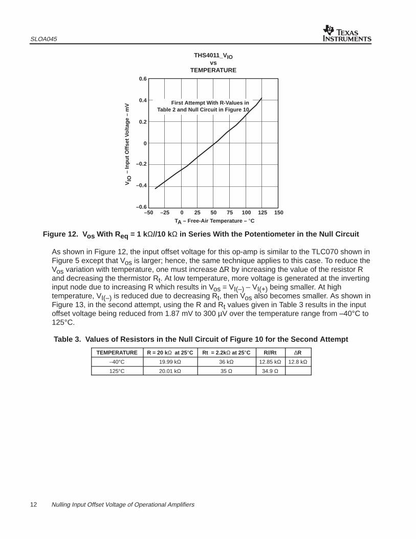
Figure 12. V os With R eq = 1 kΩ//10 kΩ in Series With the Potentiometer in the Null Circuit
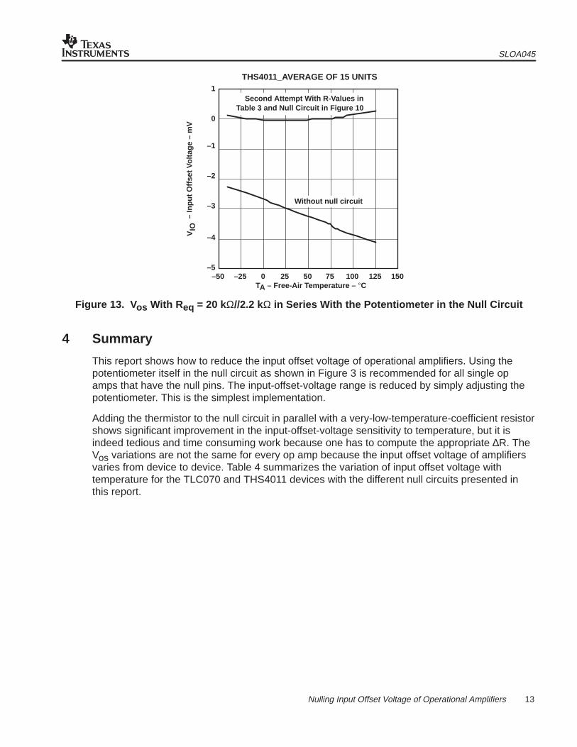
As shown in Figure 12, the input offset voltage for this op-amp is similar to the TLC070 shown inFigure 5 except that Vos is larger; hence, the same technique applies to this case. To reduce theVos variation with temperature, one must increase ∆R by increasing the value of the resistor Rand decreasing the thermistor Rt. At low temperature, more voltage is generated at the invertinginput node due to increasing R which results in Vos = VI(–) – VI(+) being smaller. At hightemperature, VI(–) is reduced due to decreasing Rt, then Vos also becomes smaller. As shown inFigure 13, in the second attempt, using the R and Rt values given in Table 3 results in the inputoffset voltage being reduced from 1.87 mV to 300 µV over the temperature range from –40°C to125°C.
Table 3. Values of Resistors in the Null Circuit of Figure 10 for the Second Attempt
TEMPERATURE R = 20 kΩ at 25°C Rt = 2.2kΩ at 25°C R//Rt ∆R
–40°C 19.99 kΩ 36 kΩ 12.85 kΩ 12.8 kΩ
125°C 20.01 kΩ 35 Ω 34.9 Ω
SLOA045
13 Nulling Input Offset Voltage of Operational Amplifiers
–5
–4
–3
–2
–1
0
1
–50 –25 0 25 50 75 100 125 150
Without null circuit
– In
put O
ffset
Vol
tage
– m
V
THS4011_AVERAGE OF 15 UNITS
TA – Free-Air Temperature – °C
VIO
Second Attempt With R-Values inTable 3 and Null Circuit in Figure 10
Figure 13. V os With R eq = 20 kΩ//2.2 kΩ in Series With the Potentiometer in the Null Circuit
4 Summary
This report shows how to reduce the input offset voltage of operational amplifiers. Using thepotentiometer itself in the null circuit as shown in Figure 3 is recommended for all single opamps that have the null pins. The input-offset-voltage range is reduced by simply adjusting thepotentiometer. This is the simplest implementation.
Adding the thermistor to the null circuit in parallel with a very-low-temperature-coefficient resistorshows significant improvement in the input-offset-voltage sensitivity to temperature, but it isindeed tedious and time consuming work because one has to compute the appropriate ∆R. TheVos variations are not the same for every op amp because the input offset voltage of amplifiersvaries from device to device. Table 4 summarizes the variation of input offset voltage withtemperature for the TLC070 and THS4011 devices with the different null circuits presented inthis report.
SLOA045
14 Nulling Input Offset Voltage of Operational Amplifiers
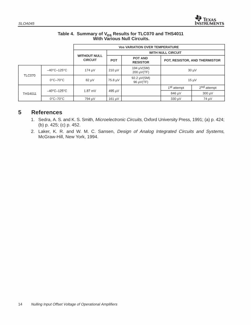
Table 4. Summary of V os Results for TLC070 and THS4011 With Various Null Circuits.
Vos VARIATION OVER TEMPERATURE
WITHOUT NULLWITH NULL CIRCUIT
WITHOUT NULLCIRCUIT POT
POT AND RESISTOR POT, RESISTOR, AND THERMISTOR
TLC070
–40°C–125°C 174 µV 210 µV194 µV(SM)200 µV(TF)
30 µV
TLC0700°C–70°C 82 µV 75.8 µV
92.2 µV(SM)96 µV(TF)
15 µV
40°C 125°C 1 87 mV 495 V1st attempt 2nd attempt
THS4011–40°C–125°C 1.87 mV 495 µV
846 µV 300 µVTHS4011
0°C–70°C 794 µV 161 µV 330 µV 74 µV
5 References1. Sedra, A. S. and K. S. Smith, Microelectronic Circuits, Oxford University Press, 1991; (a) p. 424;
(b) p. 425; (c) p. 452.
2. Laker, K. R. and W. M. C. Sansen, Design of Analog Integrated Circuits and Systems,McGraw-Hill, New York, 1994.
IMPORTANT NOTICE
Texas Instruments and its subsidiaries (TI) reserve the right to make changes to their products or to discontinueany product or service without notice, and advise customers to obtain the latest version of relevant informationto verify, before placing orders, that information being relied on is current and complete. All products are soldsubject to the terms and conditions of sale supplied at the time of order acknowledgment, including thosepertaining to warranty, patent infringement, and limitation of liability.
TI warrants performance of its semiconductor products to the specifications applicable at the time of sale inaccordance with TI’s standard warranty. Testing and other quality control techniques are utilized to the extentTI deems necessary to support this warranty. Specific testing of all parameters of each device is not necessarilyperformed, except those mandated by government requirements.
Customers are responsible for their applications using TI components.
In order to minimize risks associated with the customer’s applications, adequate design and operatingsafeguards must be provided by the customer to minimize inherent or procedural hazards.
TI assumes no liability for applications assistance or customer product design. TI does not warrant or representthat any license, either express or implied, is granted under any patent right, copyright, mask work right, or otherintellectual property right of TI covering or relating to any combination, machine, or process in which suchsemiconductor products or services might be or are used. TI’s publication of information regarding any thirdparty’s products or services does not constitute TI’s approval, warranty or endorsement thereof.
Copyright 2000, Texas Instruments Incorporated


![A Novel Digital Calibration Technique for Gain and Offset ......ΣΔ modulators. The input signal x[n] is distributed among the M modulators through an analog multiplexer. Then, the](https://static.fdocument.org/doc/165x107/60ee77b99c0fd85f564bb9e6/a-novel-digital-calibration-technique-for-gain-and-offset-modulators.jpg)