N-channel 60 V, 0.22 typ., 38 A STripFET II Power MOSFET ......Doc ID 10428 Rev 2 5/15 Table 8....
15
This is information on a product in full production. November 2012 Doc ID 10428 Rev 2 1/15 15 STB45NF06 N-channel 60 V, 0.22 Ω typ., 38 A STripFET™ II Power MOSFET in a D 2 PAK package Datasheet — production data Features ■ Typical R DS(on) = 0.022 Ω ■ Exceptional dv/dt capability ■ 100% avalanche tested ■ Standard threshold drive Applications ■ Switching applications Description This Power MOSFET has been developed using STMicroelectronics’ unique STripFET process, which is specifically designed to minimize input capacitance and gate charge. This renders the device suitable for use as primary switch in advanced high-efficiency isolated DC-DC converters for telecom and computer applications, and applications with low gate charge driving requirements. Figure 1. Internal schematic diagram Order code V DS R DS(on) max I D STB45NF06T4 60 V 0.028 Ω 38 A D 2 PAK 1 3 TAB Table 1. Device summary Order code Marking Package Packaging STB45NF06T4 B45NF06 D 2 PAK Tape and reel www.st.com
Transcript of N-channel 60 V, 0.22 typ., 38 A STripFET II Power MOSFET ......Doc ID 10428 Rev 2 5/15 Table 8....
This is information on a product in full production.
November 2012 Doc ID 10428 Rev 2 1/15
15
STB45NF06
N-channel 60 V, 0.22 Ω typ., 38 A STripFET™ II Power MOSFET in a D2PAK package
Datasheet — production data
Features
■ Typical RDS(on) = 0.022 Ω■ Exceptional dv/dt capability
■ 100% avalanche tested
■ Standard threshold drive
Applications■ Switching applications
DescriptionThis Power MOSFET has been developed using STMicroelectronics’ unique STripFET process, which is specifically designed to minimize input capacitance and gate charge. This renders the device suitable for use as primary switch in advanced high-efficiency isolated DC-DC converters for telecom and computer applications, and applications with low gate charge driving requirements.
Figure 1. Internal schematic diagram
Order code VDSRDS(on)
maxID
STB45NF06T4 60 V 0.028 Ω 38 A
D2PAK
13
TAB
Table 1. Device summary
Order code Marking Package Packaging
STB45NF06T4 B45NF06 D2PAK Tape and reel
www.st.com
Contents STB45NF06
2/15 Doc ID 10428 Rev 2
Contents
1 Electrical ratings . . . . . . . . . . . . . . . . . . . . . . . . . . . . . . . . . . . . . . . . . . . . 3
2 Electrical characteristics . . . . . . . . . . . . . . . . . . . . . . . . . . . . . . . . . . . . . 4
2.1 Electrical characteristics (curves) . . . . . . . . . . . . . . . . . . . . . . . . . . . 6
3 Test circuits . . . . . . . . . . . . . . . . . . . . . . . . . . . . . . . . . . . . . . . . . . . . . . 8
4 Package mechanical data . . . . . . . . . . . . . . . . . . . . . . . . . . . . . . . . . . . . . 9
5 Packaging mechanical data . . . . . . . . . . . . . . . . . . . . . . . . . . . . . . . . . . 12
6 Revision history . . . . . . . . . . . . . . . . . . . . . . . . . . . . . . . . . . . . . . . . . . . 14
STB45NF06 Electrical ratings
Doc ID 10428 Rev 2 3/15
1 Electrical ratings
Table 2. Absolute maximum ratings
Symbol Parameter Value Unit
VDS Drain-source voltage 60 V
VDGR Drain-gate voltage (RGS=20 kΩ) 60 V
VGS Gate-source voltage ± 20 V
ID Drain current (continuous) at TC = 25 °C 38 A
ID Drain current (continuous) at TC = 100 °C 26 A
IDM (1)
1. Pulse width limited by safe operating area
Drain current (pulsed) 152 A
PTOT Total dissipation at TC = 25 °C 80 W
Derating factor 0.53 W/°C
dv/dt (2)
2. ISD ≤ 38 A, di/dt ≤ 300 A/µs; VDS(peak) < V(BR)DSS , VDD=80 % V(BR)DSS
Peak diode recovery voltage slope 7 V/ns
Tstg Storage temperature - 65 to 175 °C
Tj Max. operating junction temperature 175 °C
Table 3. Thermal data
Symbol Parameter Value Unit
Rthj-case Thermal resistance junction-case max 1.88 °C/W
Rthj-amb(1)
1. When mounted on 1 inch² FR-4, 2 Oz copper board.
Thermal resistance junction-ambient max 35 °C/W
Table 4. Avalanche characteristics
Symbol Parameter Value Unit
IARAvalanche current, repetetive or not repetetive (pulse width limited by Tjmax )
38 A
EASSingle pulse avalanche energy (starting TJ = 25 °C, ID= IAR; VDD=50 V)
135 mJ
Electrical characteristics STB45NF06
4/15 Doc ID 10428 Rev 2
2 Electrical characteristics
(TC = 25 °C unless otherwise specified).
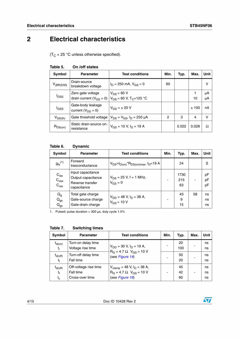
Table 5. On /off states
Symbol Parameter Test conditions Min. Typ. Max. Unit
V(BR)DSSDrain-source breakdown voltage
ID = 250 mA, VGS = 0 60 V
IDSSZero gate voltage drain current (VGS = 0)
VDS = 60 VVDS = 60 V, TC=125 °C
110
µAµA
IGSSGate-body leakagecurrent (VDS = 0)
VGS = ± 20 V ± 100 nA
VGS(th) Gate threshold voltage VDS = VGS, ID = 250 µA 2 3 4 V
RDS(on)Static drain-source on-resistance
VGS = 10 V, ID = 19 A 0.022 0.028 Ω
Table 6. Dynamic
Symbol Parameter Test conditions Min. Typ. Max. Unit
gfs(1)
1. Pulsed: pulse duration = 300 µs, duty cycle 1.5%
Forward trasconductance
VDS>ID(on)*RDS(on)max, ID=19 A 24 S
Ciss
Coss
Crss
Input capacitanceOutput capacitanceReverse transfer capacitance
VDS = 25 V, f = 1 MHz, VGS = 0
-173021563
-pFpFpF
Qg
Qgs
Qgs
Total gate chargeGate-source chargeGate-drain charge
VDD = 48 V, ID = 38 A, VGS = 10 V
-439
15
58 nsnsns
Table 7. Switching times
Symbol Parameter Test conditions Min. Typ. Max. Unit
td(on)
tr
Turn-on delay time
Voltage rise time VDD = 30 V, ID = 19 A,
RG = 4.7 Ω, VGS = 10 V(see Figure 14)
-20
100-
ns
ns
td(off)
tf
Turn-off delay time
Fall time -
50
20-
ns
ns
td(off)
tftc
Off-voltage rise time
Fall timeCross-over time
Vclamp = 48 V, ID = 38 A,
RG = 4.7 Ω, VGS = 10 V(see Figure 16)
-
45
4260
-
ns
nsns
STB45NF06 Electrical characteristics
Doc ID 10428 Rev 2 5/15
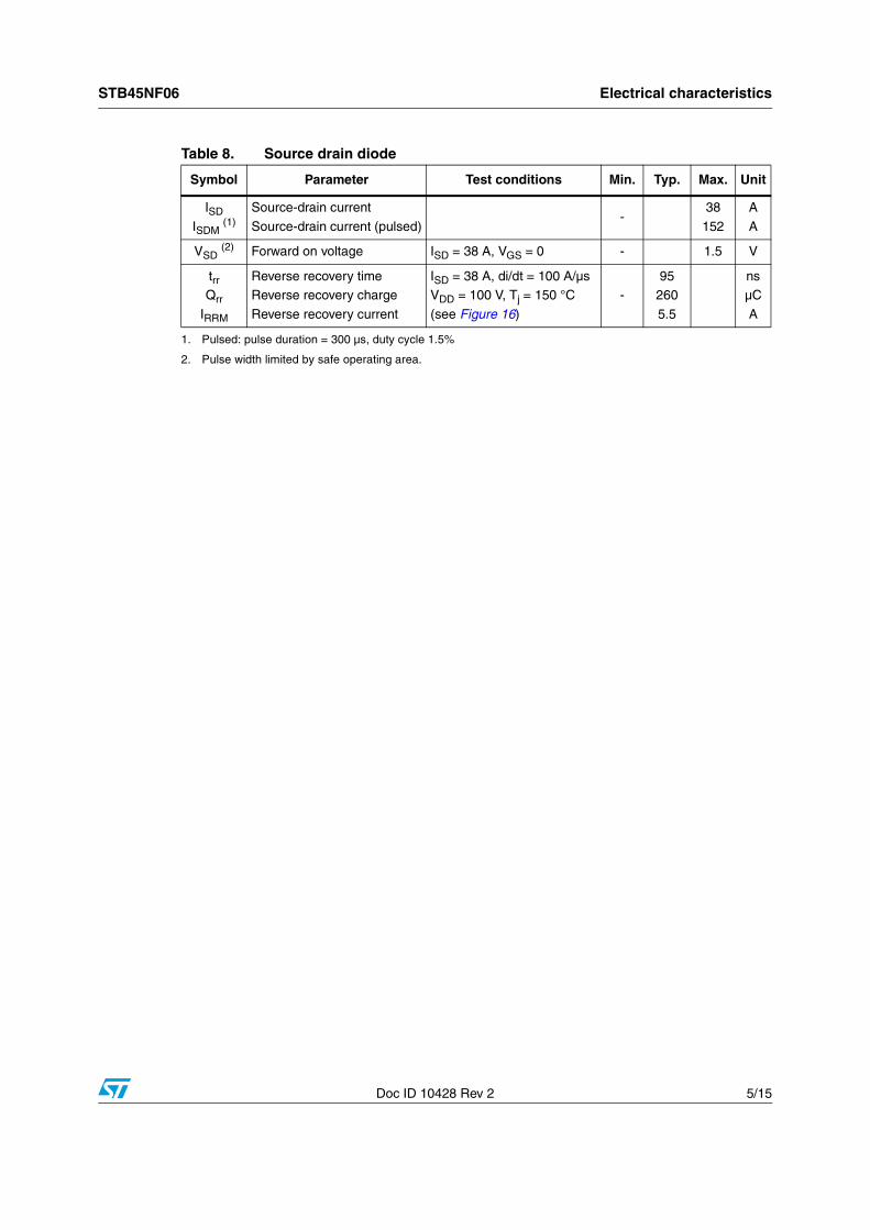
Table 8. Source drain diode
Symbol Parameter Test conditions Min. Typ. Max. Unit
ISD
ISDM (1)
1. Pulsed: pulse duration = 300 µs, duty cycle 1.5%
Source-drain current
Source-drain current (pulsed)-
38
152
A
A
VSD (2)
2. Pulse width limited by safe operating area.
Forward on voltage ISD = 38 A, VGS = 0 - 1.5 V
trrQrr
IRRM
Reverse recovery timeReverse recovery charge
Reverse recovery current
ISD = 38 A, di/dt = 100 A/µsVDD = 100 V, Tj = 150 °C
(see Figure 16)
-95
260
5.5
nsµC
A
Electrical characteristics STB45NF06
6/15 Doc ID 10428 Rev 2
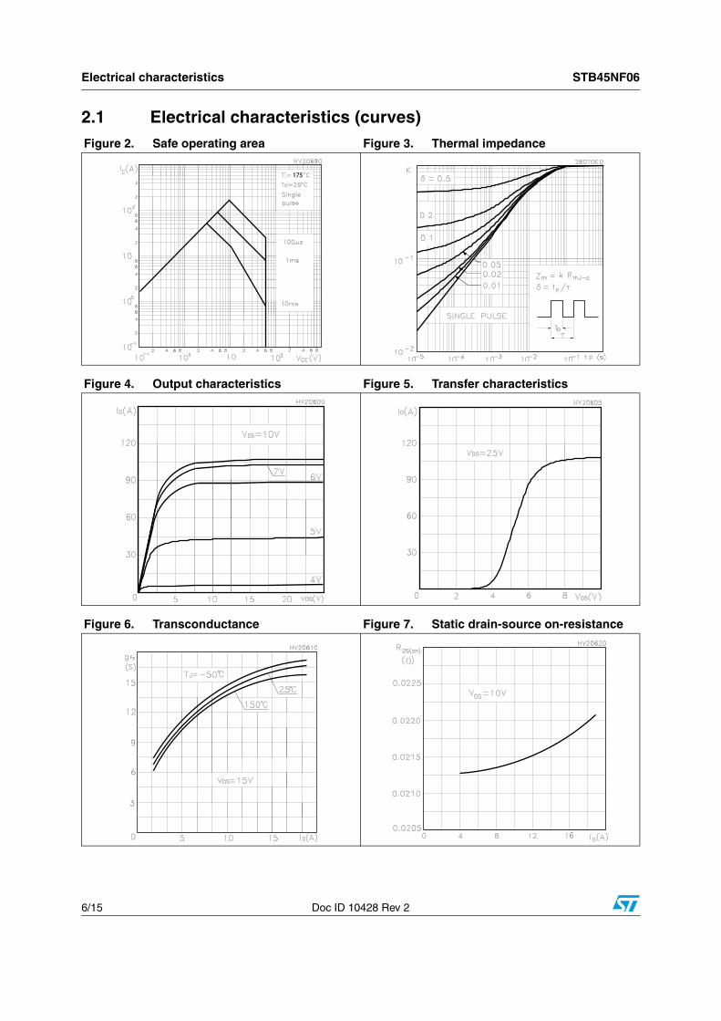
2.1 Electrical characteristics (curves) Figure 2. Safe operating area Figure 3. Thermal impedance
Figure 4. Output characteristics Figure 5. Transfer characteristics
Figure 6. Transconductance Figure 7. Static drain-source on-resistance
175175
STB45NF06 Electrical characteristics
Doc ID 10428 Rev 2 7/15
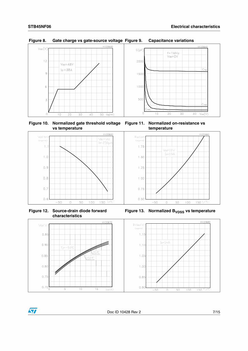
Figure 8. Gate charge vs gate-source voltage Figure 9. Capacitance variations
Figure 10. Normalized gate threshold voltage vs temperature
Figure 11. Normalized on-resistance vs temperature
Figure 12. Source-drain diode forward characteristics
Figure 13. Normalized BVDSS vs temperature
Test circuits STB45NF06
8/15 Doc ID 10428 Rev 2
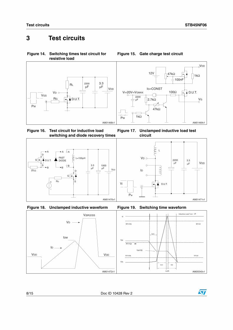
3 Test circuits
Figure 14. Switching times test circuit for resistive load
Figure 15. Gate charge test circuit
Figure 16. Test circuit for inductive load switching and diode recovery times
Figure 17. Unclamped inductive load test circuit
Figure 18. Unclamped inductive waveform Figure 19. Switching time waveform
AM01468v1
VGS
PW
VD
RG
RL
D.U.T.
2200
μF3.3μF
VDD
AM01469v1
VDD
47kΩ 1kΩ
47kΩ
2.7kΩ
1kΩ
12V
Vi=20V=VGMAX
2200μF
PW
IG=CONST100Ω
100nF
D.U.T.
VG
AM01470v1
AD
D.U.T.
SB
G
25 Ω
A A
BB
RG
G
FASTDIODE
D
S
L=100μH
μF3.3 1000
μF VDD
AM01471v1
Vi
Pw
VD
ID
D.U.T.
L
2200μF
3.3μF VDD
AM01472v1
V(BR)DSS
VDDVDD
VD
IDM
ID
AM05540v1
Inductive Load Turn - off
Id
Vgs
Vds
90%Vds
10%Id
90%Vgs on
td(v)
tc(off)
10%Vds
90%Id
Vgs(I(t))
on
tf(i)tr(v)
))
STB45NF06 Package mechanical data
Doc ID 10428 Rev 2 9/15
4 Package mechanical data
In order to meet environmental requirements, ST offers these devices in different grades of ECOPACK® packages, depending on their level of environmental compliance. ECOPACK® specifications, grade definitions and product status are available at: www.st.com. ECOPACK® is an ST trademark.
Package mechanical data STB45NF06
10/15 Doc ID 10428 Rev 2
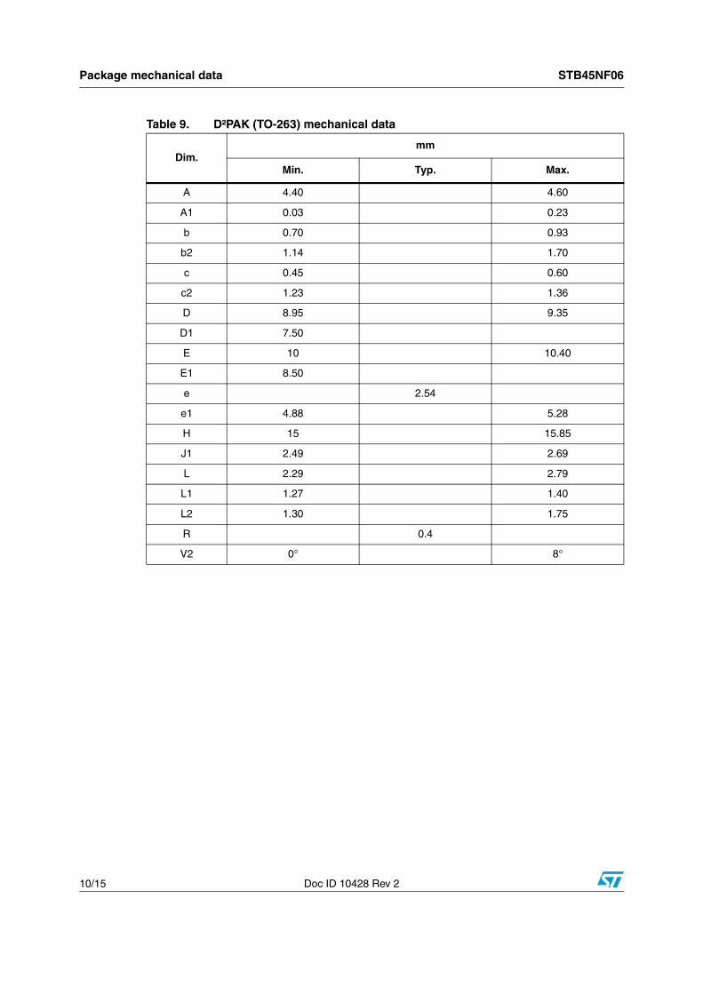
Table 9. D²PAK (TO-263) mechanical data
Dim.mm
Min. Typ. Max.
A 4.40 4.60
A1 0.03 0.23
b 0.70 0.93
b2 1.14 1.70
c 0.45 0.60
c2 1.23 1.36
D 8.95 9.35
D1 7.50
E 10 10.40
E1 8.50
e 2.54
e1 4.88 5.28
H 15 15.85
J1 2.49 2.69
L 2.29 2.79
L1 1.27 1.40
L2 1.30 1.75
R 0.4
V2 0° 8°
STB45NF06 Package mechanical data
Doc ID 10428 Rev 2 11/15
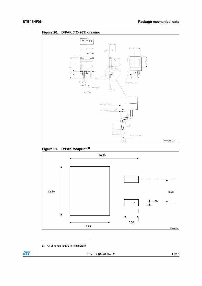
Figure 20. D²PAK (TO-263) drawing
Figure 21. D²PAK footprint(a)
a. All dimensions are in millimeters
0079457_T
16.90
12.20
9.75
3.50
5.08
1.60
Footprint
Packaging mechanical data STB45NF06
12/15 Doc ID 10428 Rev 2
5 Packaging mechanical data
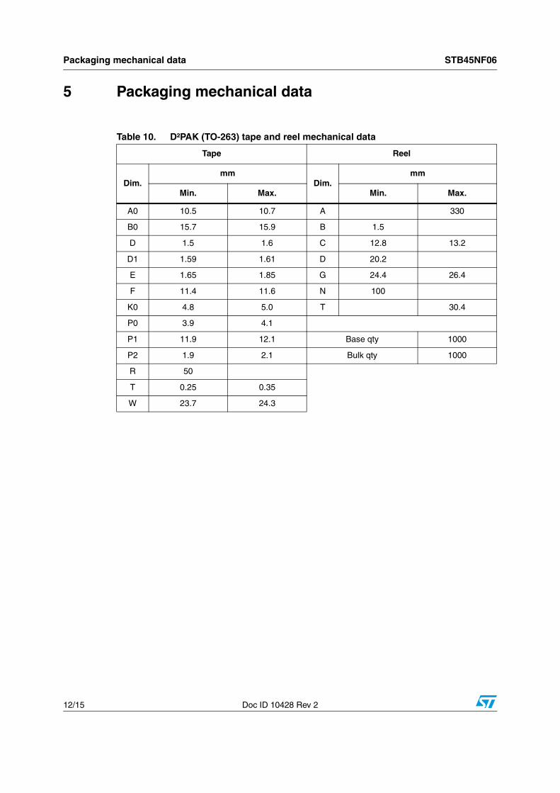
Table 10. D²PAK (TO-263) tape and reel mechanical data
Tape Reel
Dim.mm
Dim.mm
Min. Max. Min. Max.
A0 10.5 10.7 A 330
B0 15.7 15.9 B 1.5
D 1.5 1.6 C 12.8 13.2
D1 1.59 1.61 D 20.2
E 1.65 1.85 G 24.4 26.4
F 11.4 11.6 N 100
K0 4.8 5.0 T 30.4
P0 3.9 4.1
P1 11.9 12.1 Base qty 1000
P2 1.9 2.1 Bulk qty 1000
R 50
T 0.25 0.35
W 23.7 24.3
STB45NF06 Packaging mechanical data
Doc ID 10428 Rev 2 13/15
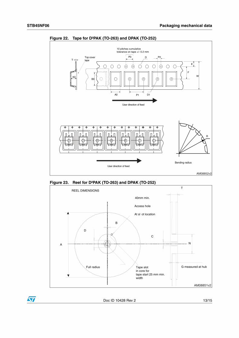
Figure 22. Tape for D²PAK (TO-263) and DPAK (TO-252)
Figure 23. Reel for D²PAK (TO-263) and DPAK (TO-252)
P1A0 D1
P0
F
W
E
D
B0K0
T
User direction of feed
P2
10 pitches cumulativetolerance on tape +/- 0.2 mm
User direction of feed
R
Bending radius
Top covertape
AM08852v2
A
D
B
Full radius G measured at hub
C
N
REEL DIMENSIONS
40mm min.
Access hole
At sl ot location
T
Tape slot in core fortape start 25 mm min.width
AM08851v2
Revision history STB45NF06
14/15 Doc ID 10428 Rev 2
6 Revision history
Table 11. Document revision history
Date Revision Changes
27-Sep-2012 1 First release.
16-Nov-2012 2– Rthj-case has been updated in table 3– Updated Section 4: Package mechanical data.– Minor text changes on cover page
STB45NF06
Doc ID 10428 Rev 2 15/15
Please Read Carefully:
Information in this document is provided solely in connection with ST products. STMicroelectronics NV and its subsidiaries (“ST”) reserve theright to make changes, corrections, modifications or improvements, to this document, and the products and services described herein at anytime, without notice.
All ST products are sold pursuant to ST’s terms and conditions of sale.
Purchasers are solely responsible for the choice, selection and use of the ST products and services described herein, and ST assumes noliability whatsoever relating to the choice, selection or use of the ST products and services described herein.
No license, express or implied, by estoppel or otherwise, to any intellectual property rights is granted under this document. If any part of thisdocument refers to any third party products or services it shall not be deemed a license grant by ST for the use of such third party productsor services, or any intellectual property contained therein or considered as a warranty covering the use in any manner whatsoever of suchthird party products or services or any intellectual property contained therein.
UNLESS OTHERWISE SET FORTH IN ST’S TERMS AND CONDITIONS OF SALE ST DISCLAIMS ANY EXPRESS OR IMPLIEDWARRANTY WITH RESPECT TO THE USE AND/OR SALE OF ST PRODUCTS INCLUDING WITHOUT LIMITATION IMPLIEDWARRANTIES OF MERCHANTABILITY, FITNESS FOR A PARTICULAR PURPOSE (AND THEIR EQUIVALENTS UNDER THE LAWSOF ANY JURISDICTION), OR INFRINGEMENT OF ANY PATENT, COPYRIGHT OR OTHER INTELLECTUAL PROPERTY RIGHT.
UNLESS EXPRESSLY APPROVED IN WRITING BY TWO AUTHORIZED ST REPRESENTATIVES, ST PRODUCTS ARE NOTRECOMMENDED, AUTHORIZED OR WARRANTED FOR USE IN MILITARY, AIR CRAFT, SPACE, LIFE SAVING, OR LIFE SUSTAININGAPPLICATIONS, NOR IN PRODUCTS OR SYSTEMS WHERE FAILURE OR MALFUNCTION MAY RESULT IN PERSONAL INJURY,DEATH, OR SEVERE PROPERTY OR ENVIRONMENTAL DAMAGE. ST PRODUCTS WHICH ARE NOT SPECIFIED AS "AUTOMOTIVEGRADE" MAY ONLY BE USED IN AUTOMOTIVE APPLICATIONS AT USER’S OWN RISK.
Resale of ST products with provisions different from the statements and/or technical features set forth in this document shall immediately voidany warranty granted by ST for the ST product or service described herein and shall not create or extend in any manner whatsoever, anyliability of ST.
ST and the ST logo are trademarks or registered trademarks of ST in various countries.
Information in this document supersedes and replaces all information previously supplied.
The ST logo is a registered trademark of STMicroelectronics. All other names are the property of their respective owners.
© 2012 STMicroelectronics - All rights reserved
STMicroelectronics group of companies
Australia - Belgium - Brazil - Canada - China - Czech Republic - Finland - France - Germany - Hong Kong - India - Israel - Italy - Japan - Malaysia - Malta - Morocco - Philippines - Singapore - Spain - Sweden - Switzerland - United Kingdom - United States of America
www.st.com

![38TYG-TYP-IOM esp[1]](https://static.fdocument.org/doc/165x107/5572017f4979599169a1b799/38tyg-typ-iom-esp1.jpg)