N-channel 650 V, 0.43 typ., 9 A MDmesh V Power MOSFET in ...
25
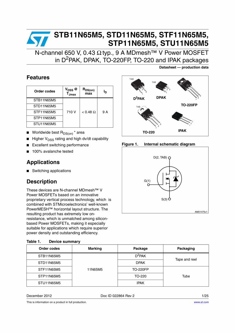
This is information on a product in full production. December 2012 Doc ID 022864 Rev 2 1/25 25 STB11N65M5, STD11N65M5, STF11N65M5, STP11N65M5, STU11N65M5 N-channel 650 V, 0.43 Ω typ., 9 A MDmesh™ V Power MOSFET in D 2 PAK, DPAK, TO-220FP, TO-220 and IPAK packages Datasheet — production data Features ■ Worldwide best R DS(on) * area ■ Higher V DSS rating and high dv/dt capability ■ Excellent switching performance ■ 100% avalanche tested Applications ■ Switching applications Description These devices are N-channel MDmesh™ V Power MOSFETs based on an innovative proprietary vertical process technology, which is combined with STMicroelectronics’ well-known PowerMESH™ horizontal layout structure. The resulting product has extremely low on- resistance, which is unmatched among silicon- based Power MOSFETs, making it especially suitable for applications which require superior power density and outstanding efficiency. Figure 1. Internal schematic diagram Order codes V DSS @ T Jmax R DS(on) max I D STB11N65M5 710 V < 0.48 Ω 9 A STD11N65M5 STF11N65M5 STP11N65M5 STU11N65M5 D 2 PAK TO-220 TO-220FP DPAK 1 3 2 TAB 1 2 3 1 2 3 TAB 1 3 TAB 2 3 2 1 IPAK Table 1. Device summary Order codes Marking Package Packaging STB11N65M5 11N65M5 D 2 PAK Tape and reel STD11N65M5 DPAK STF11N65M5 TO-220FP Tube STP11N65M5 TO-220 STU11N65M5 IPAK www.st.com
Transcript of N-channel 650 V, 0.43 typ., 9 A MDmesh V Power MOSFET in ...
This is information on a product in full production.
December 2012 Doc ID 022864 Rev 2 1/25
25
STB11N65M5, STD11N65M5, STF11N65M5, STP11N65M5, STU11N65M5
N-channel 650 V, 0.43 Ω typ., 9 A MDmesh™ V Power MOSFET in D2PAK, DPAK, TO-220FP, TO-220 and IPAK packages
Datasheet — production data
Features
■ Worldwide best RDS(on) * area
■ Higher VDSS rating and high dv/dt capability
■ Excellent switching performance
■ 100% avalanche tested
Applications■ Switching applications
DescriptionThese devices are N-channel MDmesh™ V Power MOSFETs based on an innovative proprietary vertical process technology, which is combined with STMicroelectronics’ well-known PowerMESH™ horizontal layout structure. The resulting product has extremely low on-resistance, which is unmatched among silicon-based Power MOSFETs, making it especially suitable for applications which require superior power density and outstanding efficiency.
Figure 1. Internal schematic diagram
Order codesVDSS @ TJmax
RDS(on) max
ID
STB11N65M5
710 V < 0.48 Ω 9 A
STD11N65M5
STF11N65M5
STP11N65M5
STU11N65M5
D2PAK
TO-220
TO-220FP
DPAK1
32
TAB
12
3
12
3
TAB
1
3
TAB
2
32
1
IPAK
Table 1. Device summary
Order codes Marking Package Packaging
STB11N65M5
11N65M5
D2PAKTape and reel
STD11N65M5 DPAK
STF11N65M5 TO-220FP
TubeSTP11N65M5 TO-220
STU11N65M5 IPAK
www.st.com
Contents STB11N65M5, STD11N65M5, STF11N65M5, STP11N65M5, STU11N65M5
2/25 Doc ID 022864 Rev 2
Contents
1 Electrical ratings . . . . . . . . . . . . . . . . . . . . . . . . . . . . . . . . . . . . . . . . . . . . 3
2 Electrical characteristics . . . . . . . . . . . . . . . . . . . . . . . . . . . . . . . . . . . . . 4
2.1 Electrical characteristics (curves) . . . . . . . . . . . . . . . . . . . . . . . . . . . . . . . 6
3 Test circuits . . . . . . . . . . . . . . . . . . . . . . . . . . . . . . . . . . . . . . . . . . . . . . 9
4 Package mechanical data . . . . . . . . . . . . . . . . . . . . . . . . . . . . . . . . . . . . 10
5 Packaging mechanical data . . . . . . . . . . . . . . . . . . . . . . . . . . . . . . . . . . 21
6 Revision history . . . . . . . . . . . . . . . . . . . . . . . . . . . . . . . . . . . . . . . . . . . 24
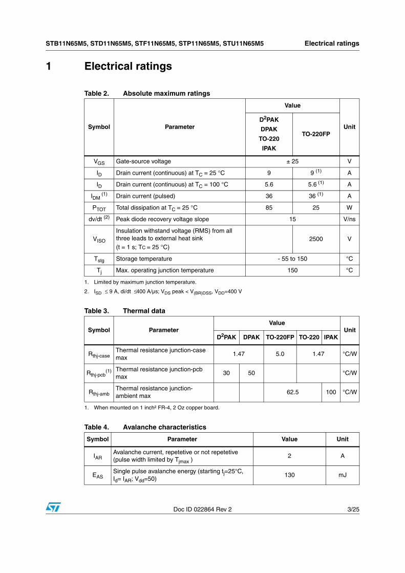
STB11N65M5, STD11N65M5, STF11N65M5, STP11N65M5, STU11N65M5 Electrical ratings
Doc ID 022864 Rev 2 3/25
1 Electrical ratings
Table 2. Absolute maximum ratings
Symbol Parameter
Value
UnitD2PAK
DPAK
TO-220
IPAK
TO-220FP
VGS Gate-source voltage ± 25 V
ID Drain current (continuous) at TC = 25 °C 9 9 (1)
1. Limited by maximum junction temperature.
A
ID Drain current (continuous) at TC = 100 °C 5.6 5.6 (1) A
IDM (1) Drain current (pulsed) 36 36 (1) A
PTOT Total dissipation at TC = 25 °C 85 25 W
dv/dt (2)
2. ISD ≤ 9 A, di/dt ≤ 400 A/µs; VDS peak < V(BR)DSS, VDD=400 V
Peak diode recovery voltage slope 15 V/ns
VISO
Insulation withstand voltage (RMS) from all three leads to external heat sink(t = 1 s; TC = 25 °C)
2500 V
Tstg Storage temperature - 55 to 150 °C
Tj Max. operating junction temperature 150 °C
Table 3. Thermal data
Symbol ParameterValue
UnitD2PAK DPAK TO-220FP TO-220 IPAK
Rthj-caseThermal resistance junction-case max
1.47 5.0 1.47 °C/W
Rthj-pcb(1)
1. When mounted on 1 inch² FR-4, 2 Oz copper board.
Thermal resistance junction-pcb max
30 50 °C/W
Rthj-ambThermal resistance junction-ambient max
62.5 100 °C/W
Table 4. Avalanche characteristics
Symbol Parameter Value Unit
IARAvalanche current, repetetive or not repetetive (pulse width limited by Tjmax )
2 A
EASSingle pulse avalanche energy (starting tj=25°C, Id= IAR; Vdd=50)
130 mJ
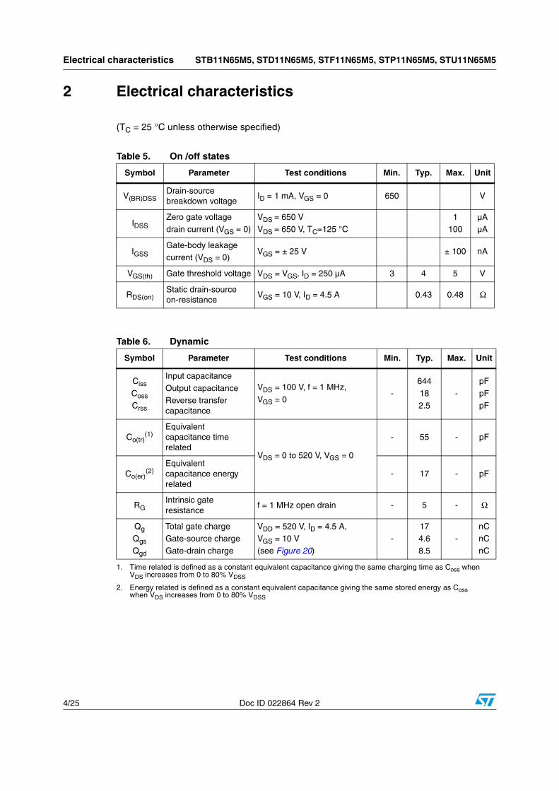
Electrical characteristics STB11N65M5, STD11N65M5, STF11N65M5, STP11N65M5, STU11N65M5
4/25 Doc ID 022864 Rev 2
2 Electrical characteristics
(TC = 25 °C unless otherwise specified)
Table 5. On /off states
Symbol Parameter Test conditions Min. Typ. Max. Unit
V(BR)DSSDrain-source breakdown voltage
ID = 1 mA, VGS = 0 650 V
IDSSZero gate voltage drain current (VGS = 0)
VDS = 650 VVDS = 650 V, TC=125 °C
1100
µAµA
IGSSGate-body leakagecurrent (VDS = 0)
VGS = ± 25 V ± 100 nA
VGS(th) Gate threshold voltage VDS = VGS, ID = 250 µA 3 4 5 V
RDS(on)Static drain-source on-resistance
VGS = 10 V, ID = 4.5 A 0.43 0.48 Ω
Table 6. Dynamic
Symbol Parameter Test conditions Min. Typ. Max. Unit
Ciss
Coss
Crss
Input capacitance
Output capacitanceReverse transfer capacitance
VDS = 100 V, f = 1 MHz,
VGS = 0-
644
182.5
-
pF
pFpF
Co(tr)(1)
1. Time related is defined as a constant equivalent capacitance giving the same charging time as Coss when VDS increases from 0 to 80% VDSS
Equivalent capacitance time related
VDS = 0 to 520 V, VGS = 0
- 55 - pF
Co(er)(2)
2. Energy related is defined as a constant equivalent capacitance giving the same stored energy as Coss when VDS increases from 0 to 80% VDSS
Equivalent capacitance energy related
- 17 - pF
RGIntrinsic gate resistance
f = 1 MHz open drain - 5 - Ω
Qg
Qgs
Qgd
Total gate chargeGate-source chargeGate-drain charge
VDD = 520 V, ID = 4.5 A,VGS = 10 V(see Figure 20)
-174.68.5
-nCnCnC
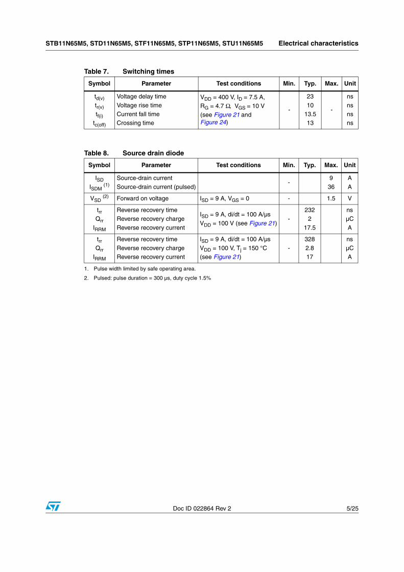
STB11N65M5, STD11N65M5, STF11N65M5, STP11N65M5, STU11N65M5 Electrical characteristics
Doc ID 022864 Rev 2 5/25
Table 7. Switching times
Symbol Parameter Test conditions Min. Typ. Max. Unit
td(v)
tr(v)
tf(i)tc(off)
Voltage delay time
Voltage rise timeCurrent fall timeCrossing time
VDD = 400 V, ID = 7.5 A, RG = 4.7 Ω, VGS = 10 V(see Figure 21 and Figure 24)
-
23
1013.513
-
ns
nsnsns
Table 8. Source drain diode
Symbol Parameter Test conditions Min. Typ. Max. Unit
ISD
ISDM (1)
1. Pulse width limited by safe operating area.
Source-drain current
Source-drain current (pulsed)-
9
36
A
A
VSD (2)
2. Pulsed: pulse duration = 300 µs, duty cycle 1.5%
Forward on voltage ISD = 9 A, VGS = 0 - 1.5 V
trrQrr
IRRM
Reverse recovery timeReverse recovery charge
Reverse recovery current
ISD = 9 A, di/dt = 100 A/µs
VDD = 100 V (see Figure 21)-
2322
17.5
nsµC
A
trrQrr
IRRM
Reverse recovery time
Reverse recovery chargeReverse recovery current
ISD = 9 A, di/dt = 100 A/µs
VDD = 100 V, Tj = 150 °C(see Figure 21)
-
328
2.817
ns
µCA
Electrical characteristics STB11N65M5, STD11N65M5, STF11N65M5, STP11N65M5, STU11N65M5
6/25 Doc ID 022864 Rev 2
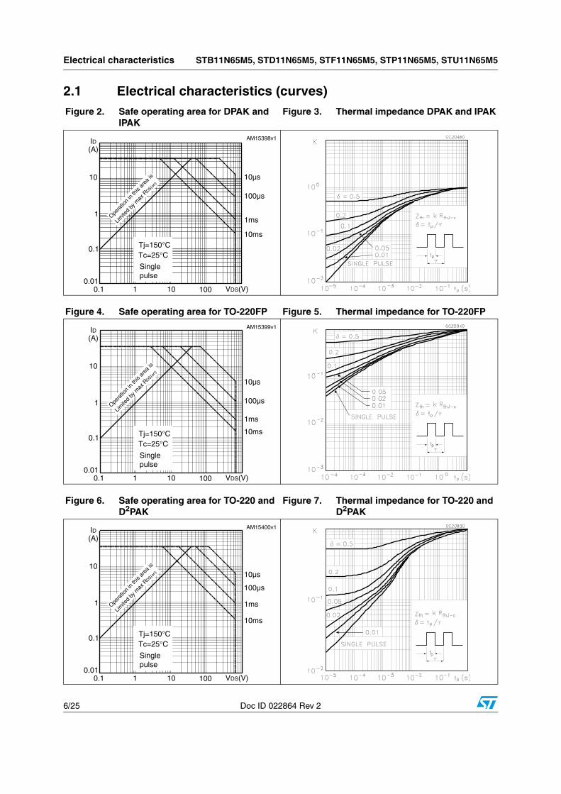
2.1 Electrical characteristics (curves)
Figure 2. Safe operating area for DPAK and IPAK
Figure 3. Thermal impedance DPAK and IPAK
ID
10
1
0.1
0.1 1 VDS(V)10
(A)
Opera
tion
in th
is ar
ea is
Limite
d by
max
RDS(o
n)
10ms
10µs
Tj=150°CTc=25°C
Singlepulse
1ms
0.01100
100µs
AM15398v1
Figure 4. Safe operating area for TO-220FP Figure 5. Thermal impedance for TO-220FP
ID
10
1
0.1
0.1 1 VDS(V)10
(A)
Opera
tion
in th
is ar
ea is
Limite
d by
max
RDS(o
n)
10ms
10µs
Tj=150°CTc=25°C
Singlepulse
1ms
0.01100
100µs
AM15399v1
Figure 6. Safe operating area for TO-220 and D2PAK
Figure 7. Thermal impedance for TO-220 and D2PAK
ID
10
1
0.1
0.1 1 VDS(V)10
(A)
Opera
tion
in th
is ar
ea is
Limite
d by
max
RDS(o
n)
10ms
10µs
Tj=150°CTc=25°C
Singlepulse
1ms
0.01100
100µs
AM15400v1
STB11N65M5, STD11N65M5, STF11N65M5, STP11N65M5, STU11N65M5 Electrical characteristics
Doc ID 022864 Rev 2 7/25
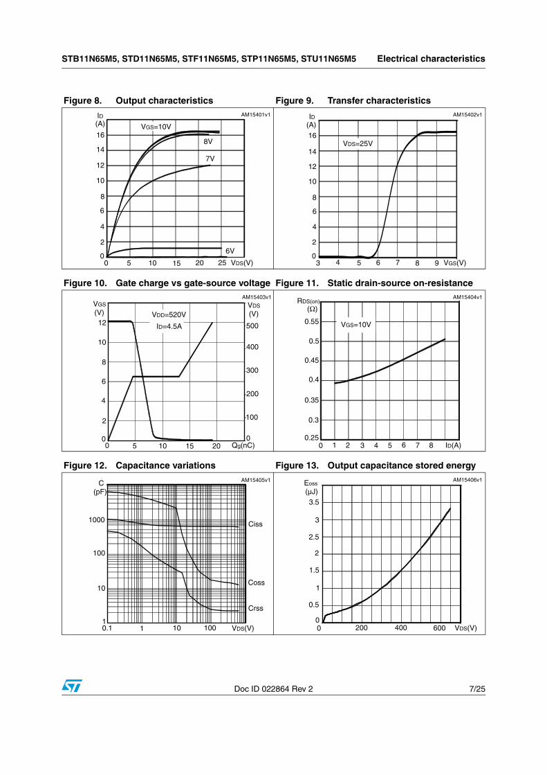
Figure 8. Output characteristics Figure 9. Transfer characteristics
Figure 10. Gate charge vs gate-source voltage Figure 11. Static drain-source on-resistance
Figure 12. Capacitance variations Figure 13. Output capacitance stored energy
ID
6
4
2
00 5 VDS(V)15
(A)
10
8
6V
7V
VGS=10V
20
8V
25
16
14
12
10
AM15401v1 ID
8
6
2
03 6 VGS(V)
(A)
4
4
5
VDS=25V
7 8 9
10
12
14
16
AM15402v1
VGS
6
4
2
00 5 Qg(nC)
(V)
8
10 15
10
VDD=520V
ID=4.5A
20
12
300
200
100
0
400
500
VDS
(V)
AM15403v1RDS(on)
0.4
0.35
0.3
0.250 2 ID(A)
(Ω)
1
0.45
0.5
VGS=10V
3 4 5 6 7 8
0.55
AM15404v1
C
100
10.1 1 VDS(V)
(pF)
10
Ciss
Coss
Crss
10
100
1000
AM15405v1 Eoss
1
0.5
00 VDS(V)
(µJ)
400
1.5
200
2
2.5
600
3
3.5
AM15406v1
Electrical characteristics STB11N65M5, STD11N65M5, STF11N65M5, STP11N65M5, STU11N65M5
8/25 Doc ID 022864 Rev 2
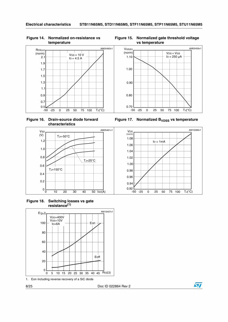
Figure 14. Normalized on-resistance vs temperature
Figure 15. Normalized gate threshold voltage vs temperature
RDS(on)
1.7
1.3
0.9
0.5-50 0 TJ(°C)
(norm)
-25 7525 50 100
0.7
1.1
1.5
1.9
2.1 ID = 4.5 AVGS = 10 V
AM05460v1 VGS(th)
1.00
0.90
0.80
0.70-50 0 TJ(°C)
(norm)
-25
1.10
7525 50 100
ID = 250 µAVDS = VGS
AM05459v1
Figure 16. Drain-source diode forward characteristics
Figure 17. Normalized BVDSS vs temperature
VSD
0 20 ISD(A)
(V)
10 5030 400
0.2
0.4
0.6
0.8
1.0
1.2
TJ=-50°C
TJ=150°C
TJ=25°C
AM05461v1 VDS
-50 0 TJ(°C)
(norm)
-25 7525 50 1000.92
0.94
0.96
0.98
1.00
1.04
1.06
1.02
ID = 1mA1.08
AM10399v1
Figure 18. Switching losses vs gate resistance(1)
1. Eon including reverse recovery of a SiC diode
E
00 20 RG(Ω)
(μJ)
10 30
20
40
40
ID=6A
VDD=400V
Eon
Eoff
60
VGS=10V
80
100
5 15 25 35 45
AM15407v1
STB11N65M5, STD11N65M5, STF11N65M5, STP11N65M5, STU11N65M5 Test circuits
Doc ID 022864 Rev 2 9/25
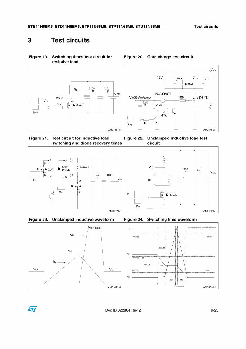
3 Test circuits
Figure 19. Switching times test circuit for resistive load
Figure 20. Gate charge test circuit
Figure 21. Test circuit for inductive load switching and diode recovery times
Figure 22. Unclamped inductive load test circuit
Figure 23. Unclamped inductive waveform Figure 24. Switching time waveform
AM05540v2
Id
Vgs
Vds
90%Vds
10%Id
90%Vgs on
Tdelay-off
TfallTrise
Tcross -over
10%Vds
90%Id
Vgs(I(t))
on
-off
TfallTrise
-
))
Concept waveform for Inductive Load Turn-off
Package mechanical data STB11N65M5, STD11N65M5, STF11N65M5, STP11N65M5, STU11N65M5
10/25 Doc ID 022864 Rev 2
4 Package mechanical data
In order to meet environmental requirements, ST offers these devices in different grades of ECOPACK® packages, depending on their level of environmental compliance. ECOPACK® specifications, grade definitions and product status are available at: www.st.com. ECOPACK® is an ST trademark.
STB11N65M5, STD11N65M5, STF11N65M5, STP11N65M5, STU11N65M5 Package mechanical data
Doc ID 022864 Rev 2 11/25
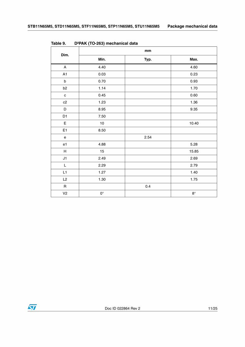
Table 9. D²PAK (TO-263) mechanical data
Dim.mm
Min. Typ. Max.
A 4.40 4.60
A1 0.03 0.23
b 0.70 0.93
b2 1.14 1.70
c 0.45 0.60
c2 1.23 1.36
D 8.95 9.35
D1 7.50
E 10 10.40
E1 8.50
e 2.54
e1 4.88 5.28
H 15 15.85
J1 2.49 2.69
L 2.29 2.79
L1 1.27 1.40
L2 1.30 1.75
R 0.4
V2 0° 8°
Package mechanical data STB11N65M5, STD11N65M5, STF11N65M5, STP11N65M5, STU11N65M5
12/25 Doc ID 022864 Rev 2
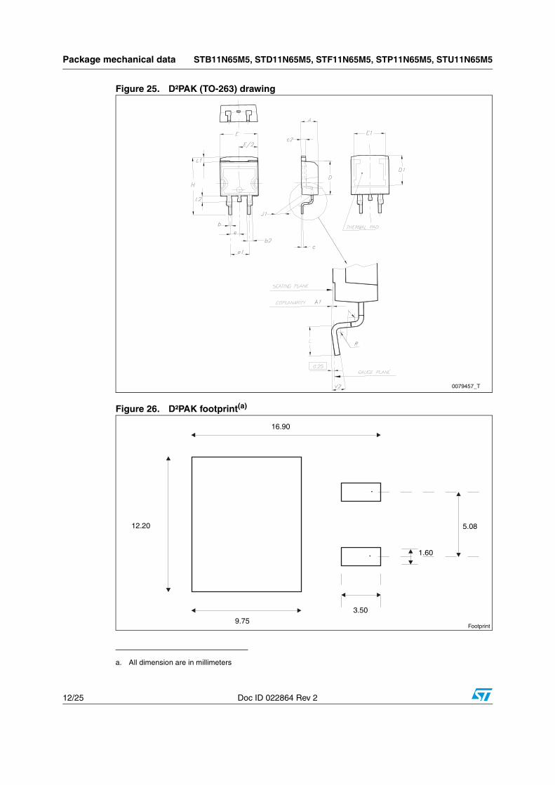
Figure 25. D²PAK (TO-263) drawing
Figure 26. D²PAK footprint(a)
a. All dimension are in millimeters
0079457_T
16.90
12.20
9.75
3.50
5.08
1.60
Footprint
STB11N65M5, STD11N65M5, STF11N65M5, STP11N65M5, STU11N65M5 Package mechanical data
Doc ID 022864 Rev 2 13/25
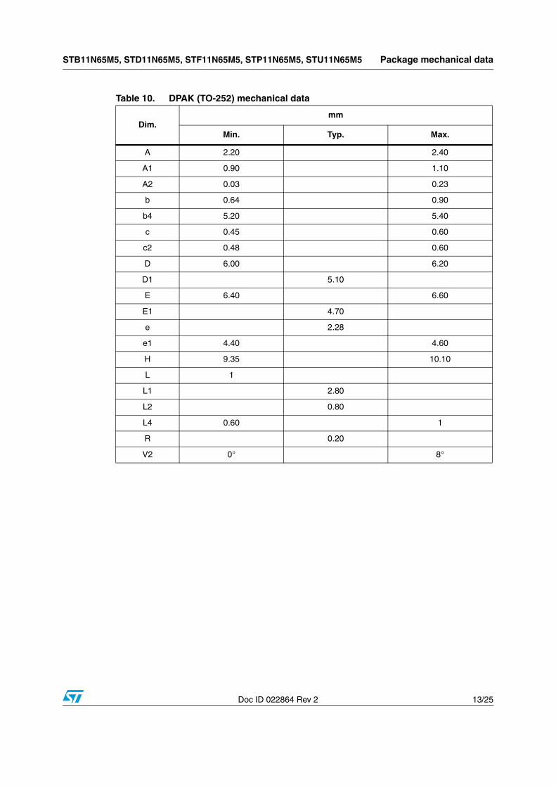
Table 10. DPAK (TO-252) mechanical data
Dim.mm
Min. Typ. Max.
A 2.20 2.40
A1 0.90 1.10
A2 0.03 0.23
b 0.64 0.90
b4 5.20 5.40
c 0.45 0.60
c2 0.48 0.60
D 6.00 6.20
D1 5.10
E 6.40 6.60
E1 4.70
e 2.28
e1 4.40 4.60
H 9.35 10.10
L 1
L1 2.80
L2 0.80
L4 0.60 1
R 0.20
V2 0° 8°
Package mechanical data STB11N65M5, STD11N65M5, STF11N65M5, STP11N65M5, STU11N65M5
14/25 Doc ID 022864 Rev 2
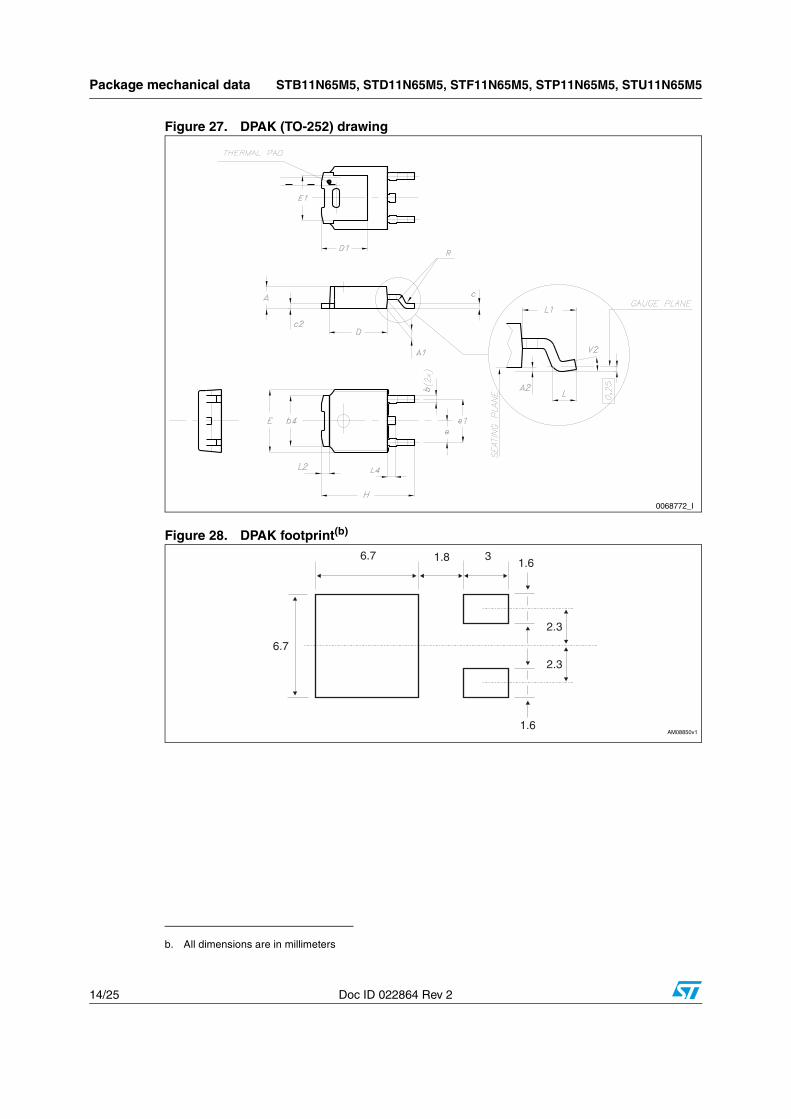
Figure 27. DPAK (TO-252) drawing
Figure 28. DPAK footprint(b)
b. All dimensions are in millimeters
0068772_I
6.7
1.6
1.6
2.3
2.3
6.7 1.8 3
AM08850v1
STB11N65M5, STD11N65M5, STF11N65M5, STP11N65M5, STU11N65M5 Package mechanical data
Doc ID 022864 Rev 2 15/25
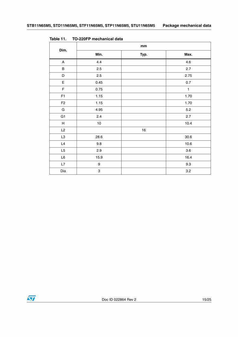
Table 11. TO-220FP mechanical data
Dim.mm
Min. Typ. Max.
A 4.4 4.6
B 2.5 2.7
D 2.5 2.75
E 0.45 0.7
F 0.75 1
F1 1.15 1.70
F2 1.15 1.70
G 4.95 5.2
G1 2.4 2.7
H 10 10.4
L2 16
L3 28.6 30.6
L4 9.8 10.6
L5 2.9 3.6
L6 15.9 16.4
L7 9 9.3
Dia 3 3.2
Package mechanical data STB11N65M5, STD11N65M5, STF11N65M5, STP11N65M5, STU11N65M5
16/25 Doc ID 022864 Rev 2
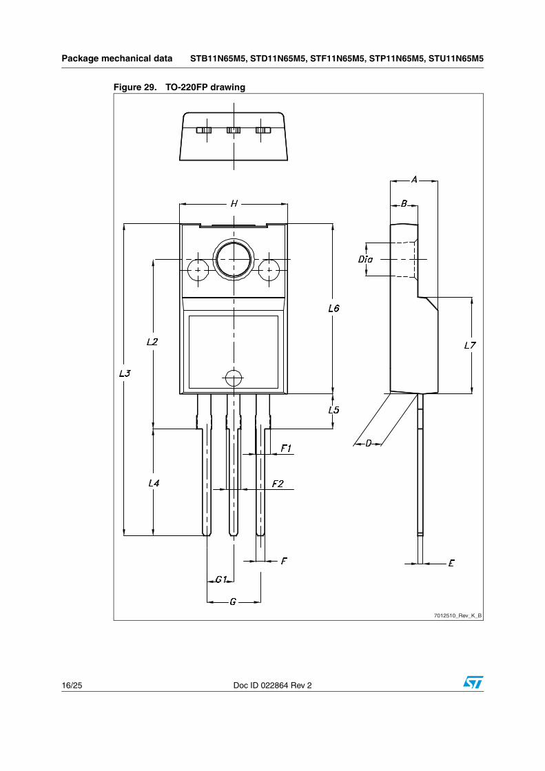
Figure 29. TO-220FP drawing
7012510_Rev_K_B
STB11N65M5, STD11N65M5, STF11N65M5, STP11N65M5, STU11N65M5 Package mechanical data
Doc ID 022864 Rev 2 17/25
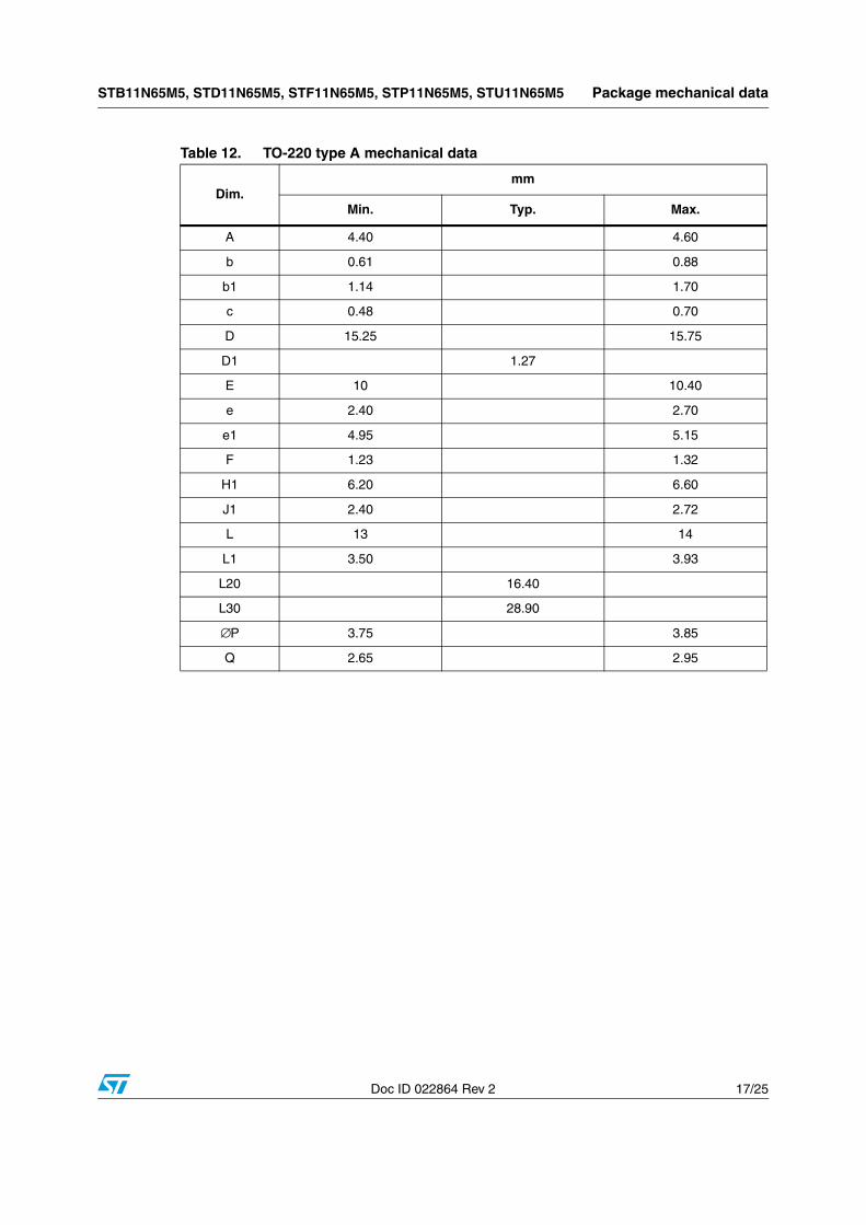
Table 12. TO-220 type A mechanical data
Dim.mm
Min. Typ. Max.
A 4.40 4.60
b 0.61 0.88
b1 1.14 1.70
c 0.48 0.70
D 15.25 15.75
D1 1.27
E 10 10.40
e 2.40 2.70
e1 4.95 5.15
F 1.23 1.32
H1 6.20 6.60
J1 2.40 2.72
L 13 14
L1 3.50 3.93
L20 16.40
L30 28.90
∅P 3.75 3.85
Q 2.65 2.95
Package mechanical data STB11N65M5, STD11N65M5, STF11N65M5, STP11N65M5, STU11N65M5
18/25 Doc ID 022864 Rev 2
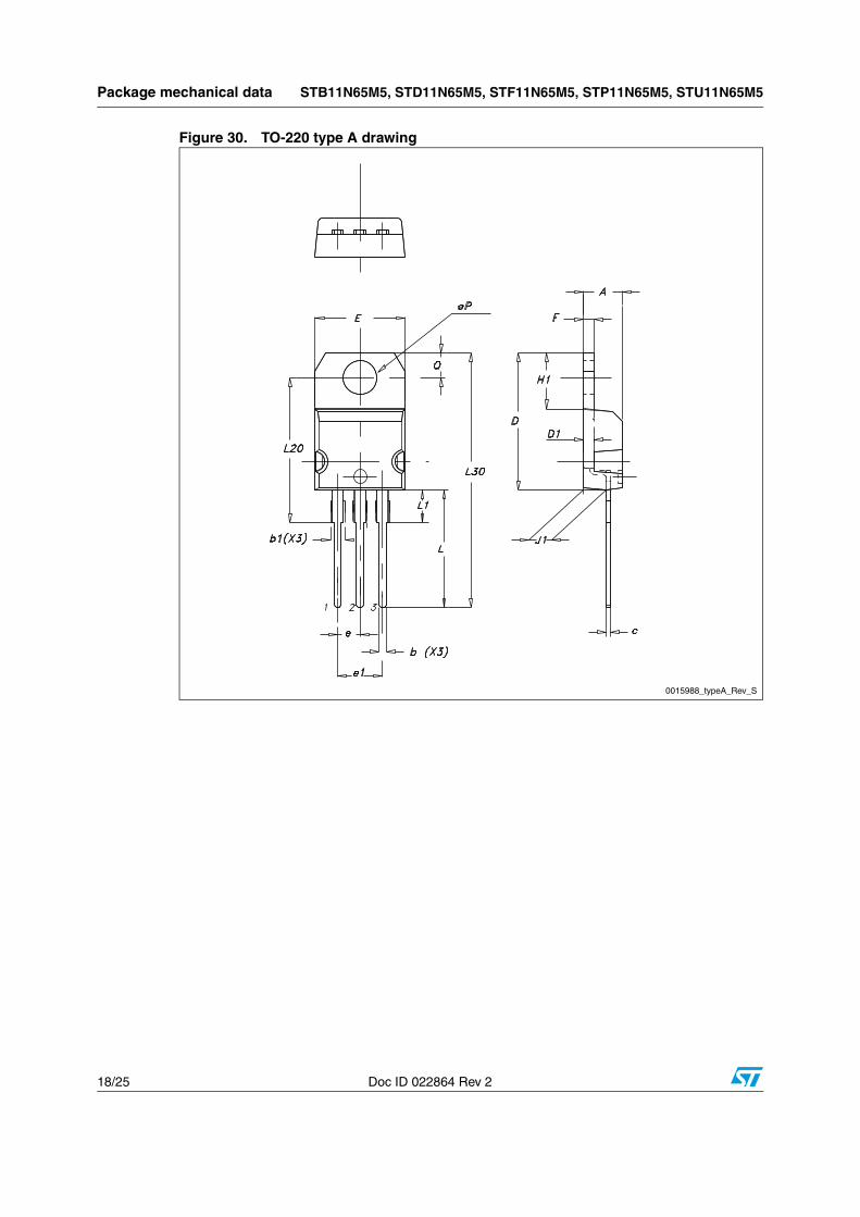
Figure 30. TO-220 type A drawing
0015988_typeA_Rev_S
STB11N65M5, STD11N65M5, STF11N65M5, STP11N65M5, STU11N65M5 Package mechanical data
Doc ID 022864 Rev 2 19/25
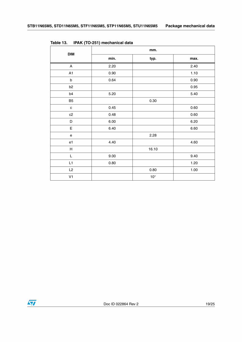
Table 13. IPAK (TO-251) mechanical data
DIMmm.
min. typ. max.
A 2.20 2.40
A1 0.90 1.10
b 0.64 0.90
b2 0.95
b4 5.20 5.40
B5 0.30
c 0.45 0.60
c2 0.48 0.60
D 6.00 6.20
E 6.40 6.60
e 2.28
e1 4.40 4.60
H 16.10
L 9.00 9.40
L1 0.80 1.20
L2 0.80 1.00
V1 10°
Package mechanical data STB11N65M5, STD11N65M5, STF11N65M5, STP11N65M5, STU11N65M5
20/25 Doc ID 022864 Rev 2
Figure 31. IPAK (TO-251) drawing
0068771_J
STB11N65M5, STD11N65M5, STF11N65M5, STP11N65M5, STU11N65M5 Packaging mechanical data
Doc ID 022864 Rev 2 21/25
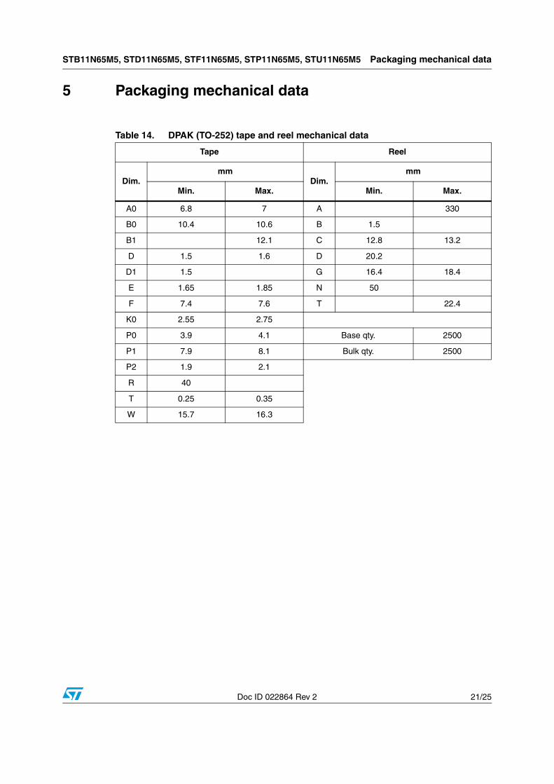
5 Packaging mechanical data
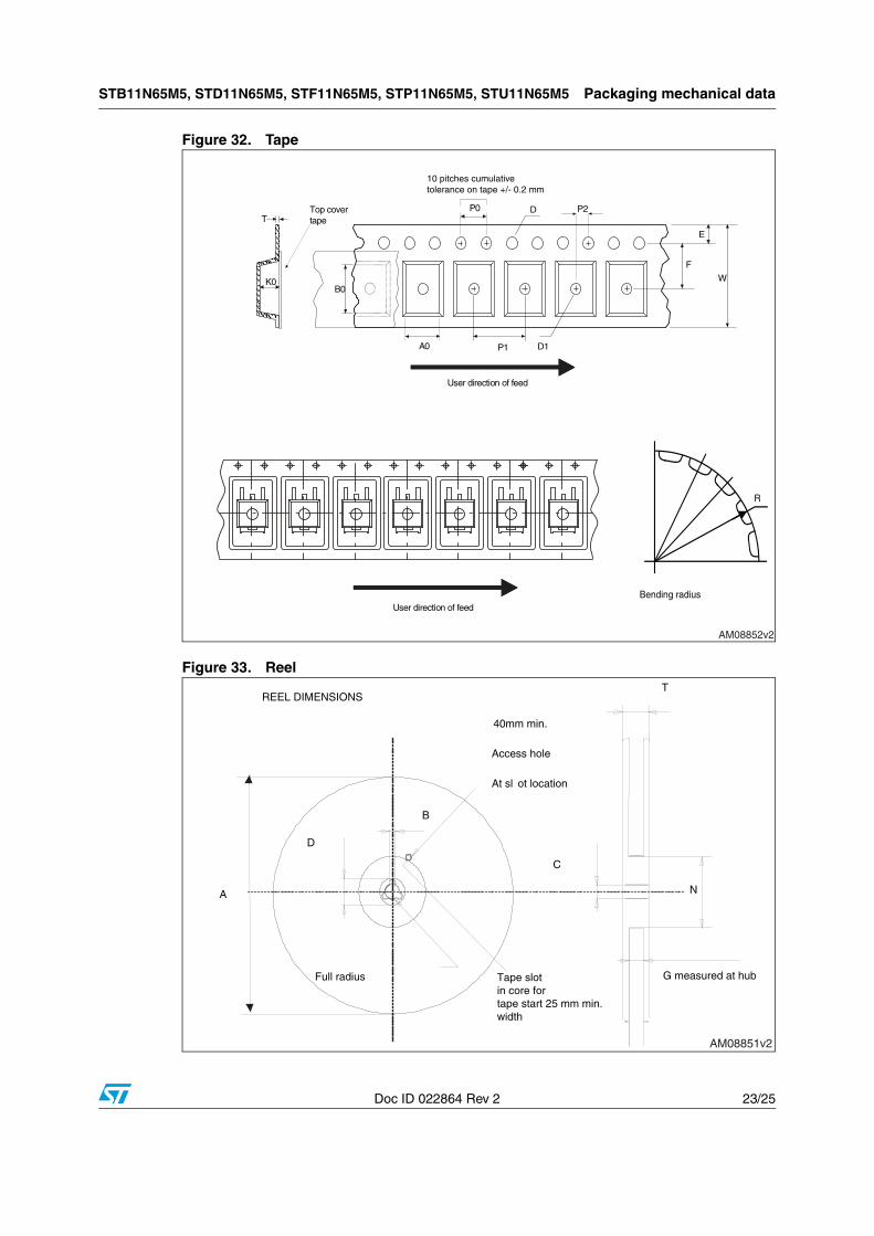
Table 14. DPAK (TO-252) tape and reel mechanical data
Tape Reel
Dim.mm
Dim.mm
Min. Max. Min. Max.
A0 6.8 7 A 330
B0 10.4 10.6 B 1.5
B1 12.1 C 12.8 13.2
D 1.5 1.6 D 20.2
D1 1.5 G 16.4 18.4
E 1.65 1.85 N 50
F 7.4 7.6 T 22.4
K0 2.55 2.75
P0 3.9 4.1 Base qty. 2500
P1 7.9 8.1 Bulk qty. 2500
P2 1.9 2.1
R 40
T 0.25 0.35
W 15.7 16.3
Packaging mechanical data STB11N65M5, STD11N65M5, STF11N65M5, STP11N65M5, STU11N65M5
22/25 Doc ID 022864 Rev 2
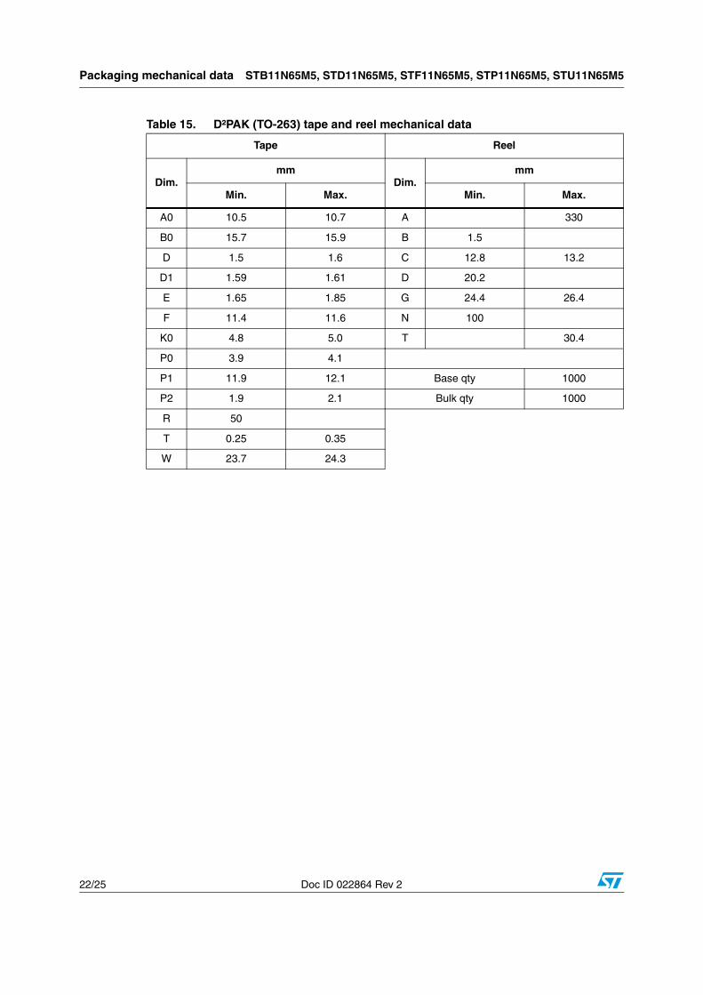
Table 15. D²PAK (TO-263) tape and reel mechanical data
Tape Reel
Dim.mm
Dim.mm
Min. Max. Min. Max.
A0 10.5 10.7 A 330
B0 15.7 15.9 B 1.5
D 1.5 1.6 C 12.8 13.2
D1 1.59 1.61 D 20.2
E 1.65 1.85 G 24.4 26.4
F 11.4 11.6 N 100
K0 4.8 5.0 T 30.4
P0 3.9 4.1
P1 11.9 12.1 Base qty 1000
P2 1.9 2.1 Bulk qty 1000
R 50
T 0.25 0.35
W 23.7 24.3
STB11N65M5, STD11N65M5, STF11N65M5, STP11N65M5, STU11N65M5 Packaging mechanical data
Doc ID 022864 Rev 2 23/25
Figure 32. Tape
Figure 33. Reel
P1A0 D1
P0
F
W
E
D
B0K0
T
User direction of feed
P2
10 pitches cumulativetolerance on tape +/- 0.2 mm
User direction of feed
R
Bending radius
Top covertape
AM08852v2
A
D
B
Full radius G measured at hub
C
N
REEL DIMENSIONS
40mm min.
Access hole
At sl ot location
T
Tape slot in core fortape start 25 mm min.width
AM08851v2
Revision history STB11N65M5, STD11N65M5, STF11N65M5, STP11N65M5, STU11N65M5
24/25 Doc ID 022864 Rev 2
6 Revision history
Table 16. Document revision history
Date Revision Changes
23-Feb-2012 1 First release.
03-Dec-2012 2
– Minor text changes in cover page– Added IPAK packages– Added Section 2.1: Electrical characteristics (curves)
– Updated Section 5: Packaging mechanical data– Modified: note 2 on Table 2– Updated: mechanical data for TO-220FP package
STB11N65M5, STD11N65M5, STF11N65M5, STP11N65M5, STU11N65M5
Doc ID 022864 Rev 2 25/25
Please Read Carefully:
Information in this document is provided solely in connection with ST products. STMicroelectronics NV and its subsidiaries (“ST”) reserve theright to make changes, corrections, modifications or improvements, to this document, and the products and services described herein at anytime, without notice.
All ST products are sold pursuant to ST’s terms and conditions of sale.
Purchasers are solely responsible for the choice, selection and use of the ST products and services described herein, and ST assumes noliability whatsoever relating to the choice, selection or use of the ST products and services described herein.
No license, express or implied, by estoppel or otherwise, to any intellectual property rights is granted under this document. If any part of thisdocument refers to any third party products or services it shall not be deemed a license grant by ST for the use of such third party productsor services, or any intellectual property contained therein or considered as a warranty covering the use in any manner whatsoever of suchthird party products or services or any intellectual property contained therein.
UNLESS OTHERWISE SET FORTH IN ST’S TERMS AND CONDITIONS OF SALE ST DISCLAIMS ANY EXPRESS OR IMPLIEDWARRANTY WITH RESPECT TO THE USE AND/OR SALE OF ST PRODUCTS INCLUDING WITHOUT LIMITATION IMPLIEDWARRANTIES OF MERCHANTABILITY, FITNESS FOR A PARTICULAR PURPOSE (AND THEIR EQUIVALENTS UNDER THE LAWSOF ANY JURISDICTION), OR INFRINGEMENT OF ANY PATENT, COPYRIGHT OR OTHER INTELLECTUAL PROPERTY RIGHT.
UNLESS EXPRESSLY APPROVED IN WRITING BY TWO AUTHORIZED ST REPRESENTATIVES, ST PRODUCTS ARE NOTRECOMMENDED, AUTHORIZED OR WARRANTED FOR USE IN MILITARY, AIR CRAFT, SPACE, LIFE SAVING, OR LIFE SUSTAININGAPPLICATIONS, NOR IN PRODUCTS OR SYSTEMS WHERE FAILURE OR MALFUNCTION MAY RESULT IN PERSONAL INJURY,DEATH, OR SEVERE PROPERTY OR ENVIRONMENTAL DAMAGE. ST PRODUCTS WHICH ARE NOT SPECIFIED AS "AUTOMOTIVEGRADE" MAY ONLY BE USED IN AUTOMOTIVE APPLICATIONS AT USER’S OWN RISK.
Resale of ST products with provisions different from the statements and/or technical features set forth in this document shall immediately voidany warranty granted by ST for the ST product or service described herein and shall not create or extend in any manner whatsoever, anyliability of ST.
ST and the ST logo are trademarks or registered trademarks of ST in various countries.
Information in this document supersedes and replaces all information previously supplied.
The ST logo is a registered trademark of STMicroelectronics. All other names are the property of their respective owners.
© 2012 STMicroelectronics - All rights reserved
STMicroelectronics group of companies
Australia - Belgium - Brazil - Canada - China - Czech Republic - Finland - France - Germany - Hong Kong - India - Israel - Italy - Japan - Malaysia - Malta - Morocco - Philippines - Singapore - Spain - Sweden - Switzerland - United Kingdom - United States of America
www.st.com