N-channel 500V - 0.22 - 20A TO-247 FDmesh Power · PDF filestw20nm50fd 2/8 thermal data...
8
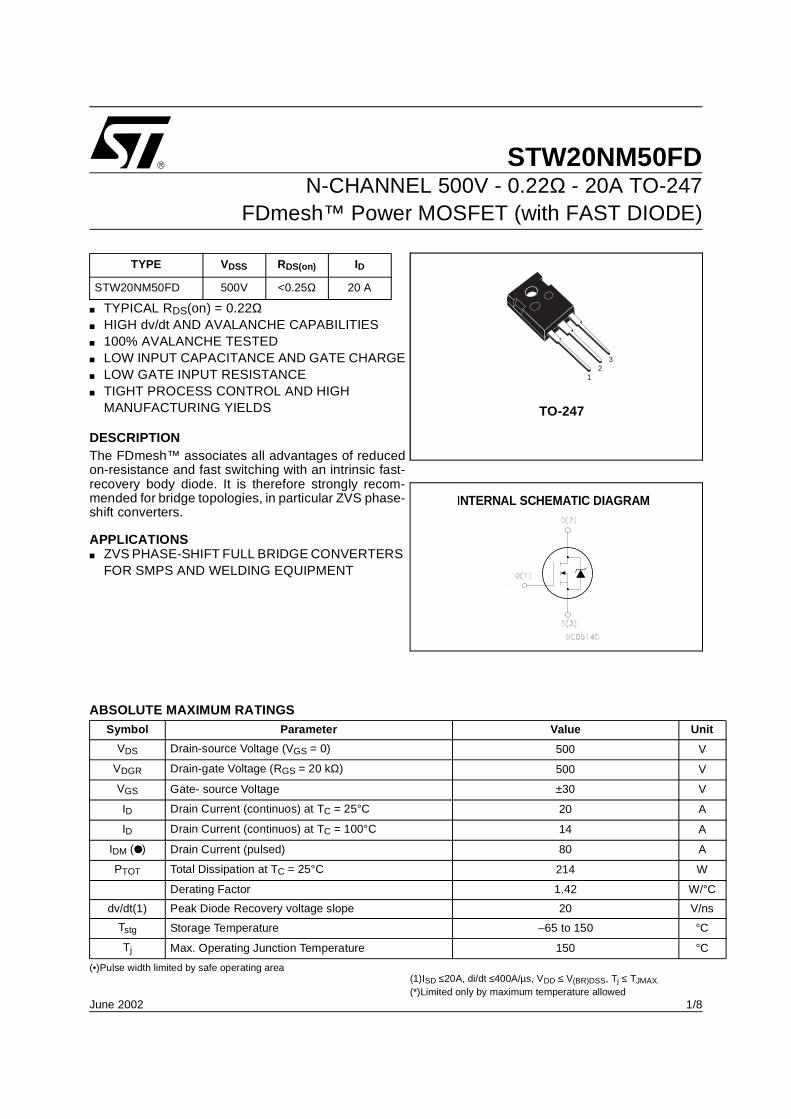
1/8 June 2002 STW20NM50FD N-CHANNEL 500V - 0.22Ω - 20A TO-247 FDmesh™ Power MOSFET (with FAST DIODE) (1)I SD ≤20A, di/dt ≤400A/μs, V DD ≤ V (BR)DSS , T j ≤ T JMAX. (*)Limited only by maximum temperature allowed ■ TYPICAL R DS (on) = 0.22Ω ■ HIGH dv/dt AND AVALANCHE CAPABILITIES ■ 100% AVALANCHE TESTED ■ LOW INPUT CAPACITANCE AND GATE CHARGE ■ LOW GATE INPUT RESISTANCE ■ TIGHT PROCESS CONTROL AND HIGH MANUFACTURING YIELDS DESCRIPTION The FDmesh™ associates all advantages of reduced on-resistance and fast switching with an intrinsic fast- recovery body diode. It is therefore strongly recom- mended for bridge topologies, in particular ZVS phase- shift converters. APPLICATIONS ■ ZVS PHASE-SHIFT FULL BRIDGE CONVERTERS FOR SMPS AND WELDING EQUIPMENT ABSOLUTE MAXIMUM RATINGS (•)Pulse width limited by safe operating area TYPE V DSS R DS(on) I D STW20NM50FD 500V <0.25Ω 20 A Symbol Parameter Value Unit V DS Drain-source Voltage (V GS = 0) 500 V V DGR Drain-gate Voltage (R GS = 20 kΩ) 500 V V GS Gate- source Voltage ±30 V I D Drain Current (continuos) at T C = 25°C 20 A I D Drain Current (continuos) at T C = 100°C 14 A I DM (●) Drain Current (pulsed) 80 A P TOT Total Dissipation at T C = 25°C 214 W Derating Factor 1.42 W/°C dv/dt(1) Peak Diode Recovery voltage slope 20 V/ns T stg Storage Temperature –65 to 150 °C T j Max. Operating Junction Temperature 150 °C TO-247 1 2 3 INTERNAL SCHEMATIC DIAGRAM
Transcript of N-channel 500V - 0.22 - 20A TO-247 FDmesh Power · PDF filestw20nm50fd 2/8 thermal data...
1/8June 2002
STW20NM50FDN-CHANNEL 500V - 0.22Ω - 20A TO-247
FDmesh™ Power MOSFET (with FAST DIODE)
(1)ISD ≤20A, di/dt ≤400A/µs, VDD ≤ V(BR)DSS, Tj ≤ TJMAX.
(*)Limited only by maximum temperature allowed
TYPICAL RDS(on) = 0.22Ω HIGH dv/dt AND AVALANCHE CAPABILITIES 100% AVALANCHE TESTED LOW INPUT CAPACITANCE AND GATE CHARGE LOW GATE INPUT RESISTANCE TIGHT PROCESS CONTROL AND HIGH
MANUFACTURING YIELDS
DESCRIPTIONThe FDmesh™ associates all advantages of reducedon-resistance and fast switching with an intrinsic fast-recovery body diode. It is therefore strongly recom-mended for bridge topologies, in particular ZVS phase-shift converters.
APPLICATIONS ZVS PHASE-SHIFT FULL BRIDGE CONVERTERS
FOR SMPS AND WELDING EQUIPMENT
ABSOLUTE MAXIMUM RATINGS
(•)Pulse width limited by safe operating area
TYPE VDSS RDS(on) ID
STW20NM50FD 500V <0.25Ω 20 A
Symbol Parameter Value Unit
VDS Drain-source Voltage (VGS = 0) 500 V
VDGR Drain-gate Voltage (RGS = 20 kΩ) 500 V
VGS Gate- source Voltage ±30 V
ID Drain Current (continuos) at TC = 25°C 20 A
ID Drain Current (continuos) at TC = 100°C 14 A
IDM () Drain Current (pulsed) 80 A
PTOT Total Dissipation at TC = 25°C 214 W
Derating Factor 1.42 W/°C
dv/dt(1) Peak Diode Recovery voltage slope 20 V/ns
Tstg Storage Temperature –65 to 150 °C
Tj Max. Operating Junction Temperature 150 °C
TO-247
12
3
INTERNAL SCHEMATIC DIAGRAM
STW20NM50FD
2/8
THERMAL DATA
AVALANCHE CHARACTERISTICS
ELECTRICAL CHARACTERISTICS (TCASE = 25 °C UNLESS OTHERWISE SPECIFIED)OFF
ON (1)
DYNAMIC
1. Pulsed: Pulse duration = 300 µs, duty cycle 1.5 %.2. Coss eq. is defined as a constant equivalent capacitance giving the same charging time as Coss when VDS increases from 0 to 80%
VDSS.
Rthj-case Thermal Resistance Junction-case Max 0.585 °C/W
Rthj-amb Thermal Resistance Junction-ambient Max 30 °C/W
Tl Maximum Lead Temperature For Soldering Purpose 300 °C
Symbol Parameter Max Value Unit
IAR Avalanche Current, Repetitive or Not-Repetitive(pulse width limited by Tj max)
10 A
EAS Single Pulse Avalanche Energy(starting Tj = 25 °C, ID = IAR, VDD = 35 V)
700 mJ
Symbol Parameter Test Conditions Min. Typ. Max. Unit
V(BR)DSS Drain-source Breakdown Voltage
ID = 250 µA, VGS = 0 500 V
IDSS Zero Gate Voltage Drain Current (VGS = 0)
VDS = Max Rating 1 µA
VDS = Max Rating, TC = 125 °C 10 µA
IGSS Gate-body LeakageCurrent (VDS = 0)
VGS = ±30V ±100 nA
Symbol Parameter Test Conditions Min. Typ. Max. Unit
VGS(th) Gate Threshold Voltage VDS = VGS, ID = 250µA 3 4 5 V
RDS(on) Static Drain-source OnResistance
VGS = 10V, ID = 10A 0.22 0.25 Ω
Symbol Parameter Test Conditions Min. Typ. Max. Unit
gfs (1) Forward Transconductance VDS > ID(on) x RDS(on)max, ID = 10A
9 S
Ciss Input Capacitance VDS = 25V, f = 1 MHz, VGS = 0 1380 pF
Coss Output Capacitance 290 pF
Crss Reverse Transfer Capacitance
40 pF
Coss eq. (2) Equivalent Output Capacitance
VGS = 0V, VDS = 0V to 400V 130 pF
Rg Gate Input Resistance f=1 MHz Gate DC Bias=0Test Signal Level=20mVOpen Drain
2.8 Ω
3/8
STW20NM50FD
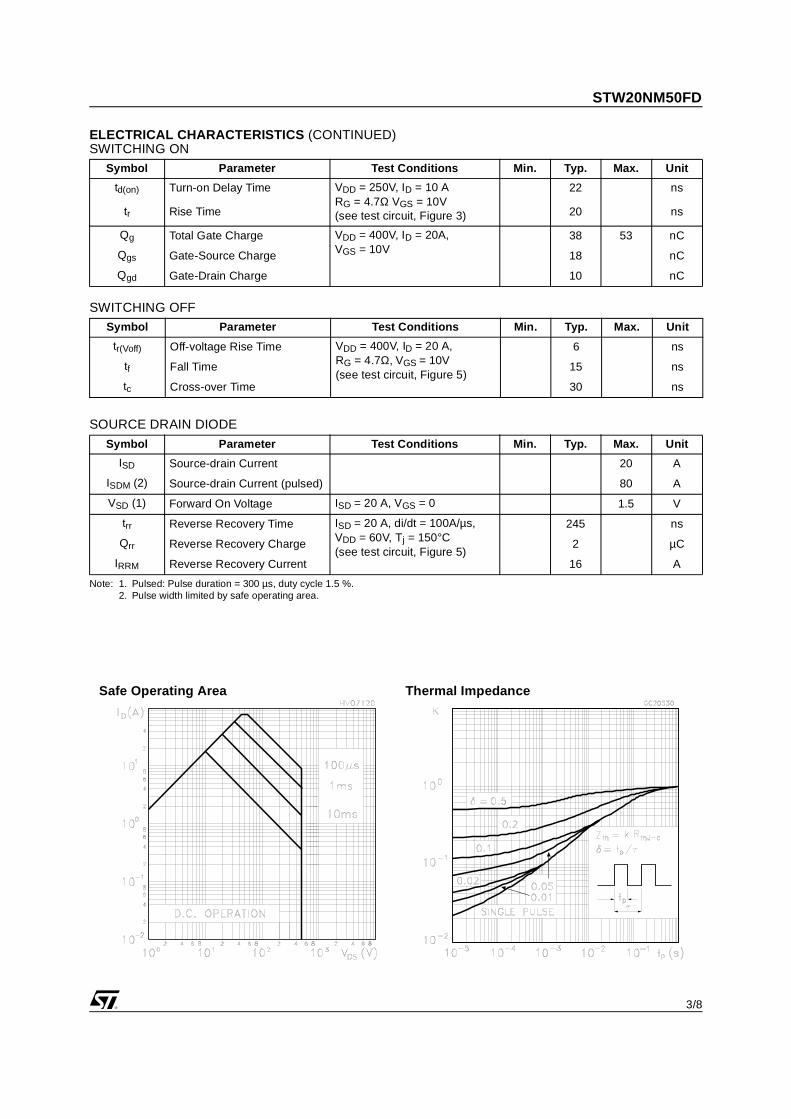
ELECTRICAL CHARACTERISTICS (CONTINUED)SWITCHING ON
SWITCHING OFF
SOURCE DRAIN DIODE
Note: 1. Pulsed: Pulse duration = 300 µs, duty cycle 1.5 %.2. Pulse width limited by safe operating area.
Symbol Parameter Test Conditions Min. Typ. Max. Unit
td(on) Turn-on Delay Time VDD = 250V, ID = 10 A RG = 4.7Ω VGS = 10V(see test circuit, Figure 3)
22 ns
tr Rise Time 20 ns
Qg Total Gate Charge VDD = 400V, ID = 20A,VGS = 10V
38 53 nC
Qgs Gate-Source Charge 18 nC
Qgd Gate-Drain Charge 10 nC
Symbol Parameter Test Conditions Min. Typ. Max. Unit
tr(Voff) Off-voltage Rise Time VDD = 400V, ID = 20 A, RG = 4.7Ω, VGS = 10V(see test circuit, Figure 5)
6 ns
tf Fall Time 15 ns
tc Cross-over Time 30 ns
Symbol Parameter Test Conditions Min. Typ. Max. Unit
ISD Source-drain Current 20 A
ISDM (2) Source-drain Current (pulsed) 80 A
VSD (1) Forward On Voltage ISD = 20 A, VGS = 0 1.5 V
trr Reverse Recovery Time ISD = 20 A, di/dt = 100A/µs, VDD = 60V, Tj = 150°C(see test circuit, Figure 5)
245 ns
Qrr Reverse Recovery Charge 2 µC
IRRM Reverse Recovery Current 16 A
Safe Operating Area Thermal Impedance
STW20NM50FD
4/8
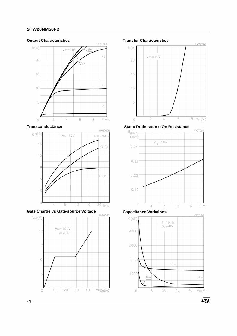
Output Characteristics
Transconductance
Transfer Characteristics
Static Drain-source On Resistance
Capacitance VariationsGate Charge vs Gate-source Voltage
5/8
STW20NM50FD
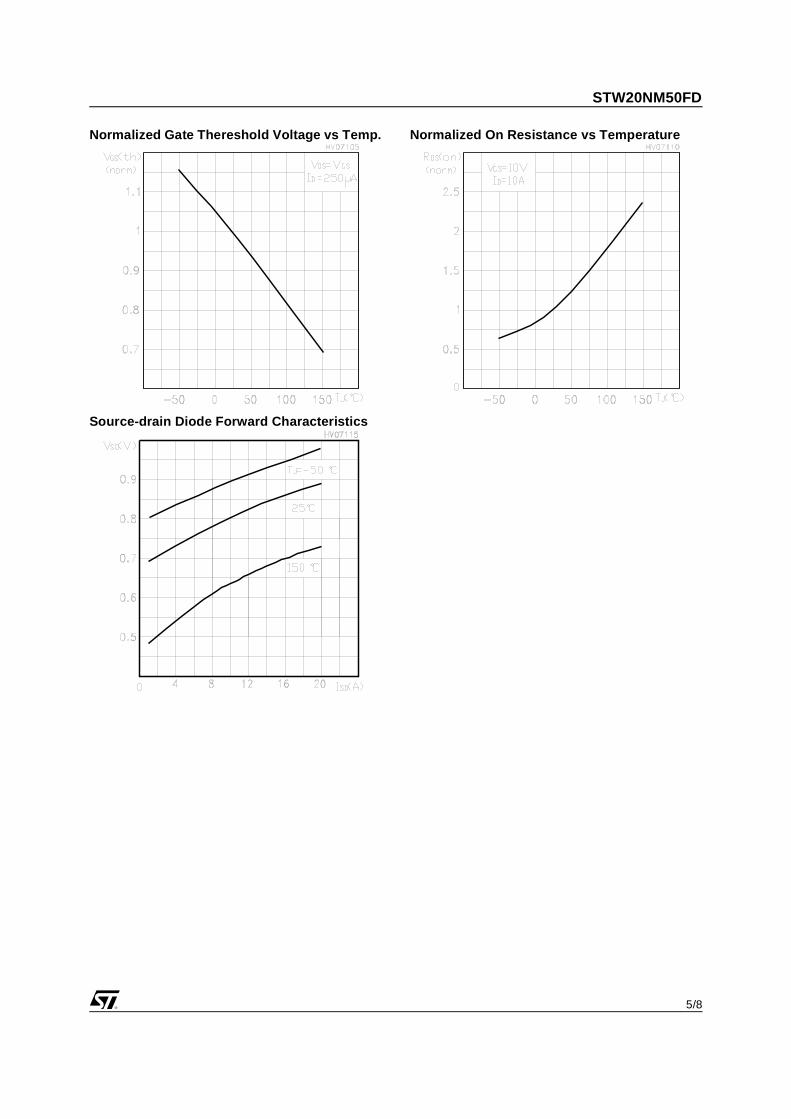
Source-drain Diode Forward Characteristics
Normalized On Resistance vs TemperatureNormalized Gate Thereshold Voltage vs Temp.
STW20NM50FD
6/8
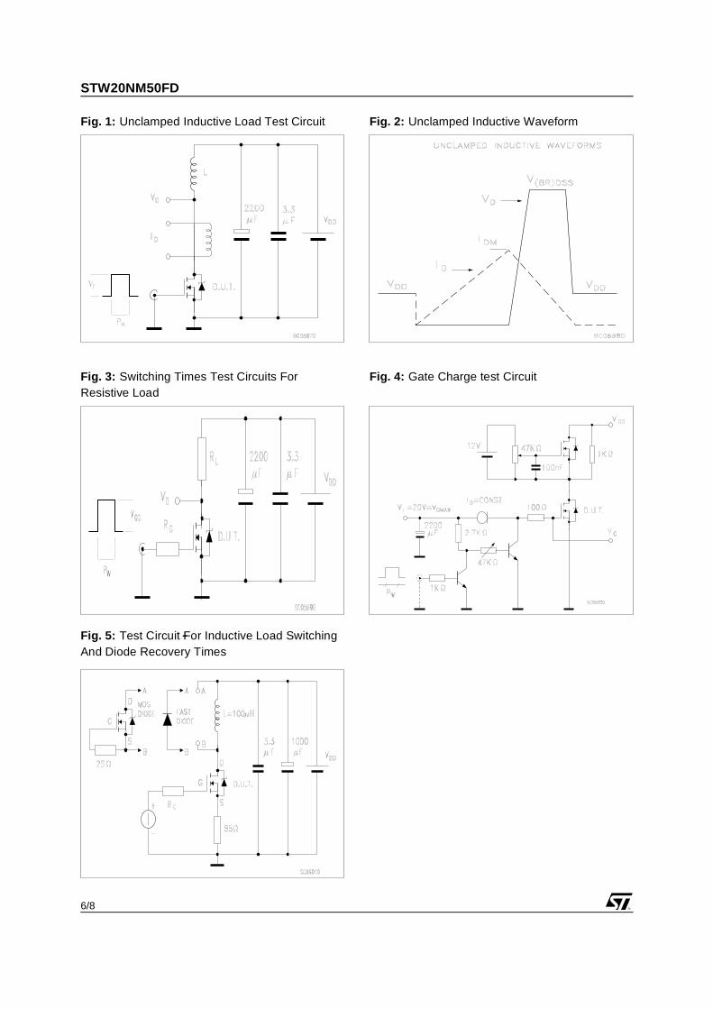
Fig. 5: Test Circuit For Inductive Load SwitchingAnd Diode Recovery Times
Fig. 4: Gate Charge test Circuit
Fig. 2: Unclamped Inductive WaveformFig. 1: Unclamped Inductive Load Test Circuit
Fig. 3: Switching Times Test Circuits For Resistive Load
7/8
STW20NM50FD
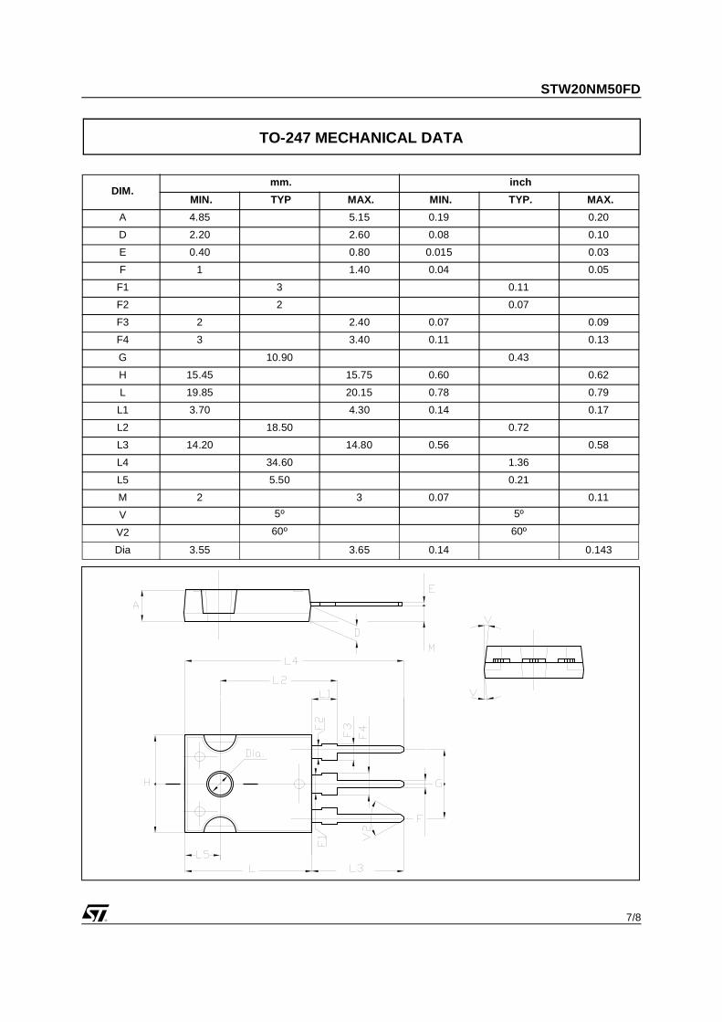
DIM.mm. inch
MIN. TYP MAX. MIN. TYP. MAX.
A 4.85 5.15 0.19 0.20
D 2.20 2.60 0.08 0.10
E 0.40 0.80 0.015 0.03
F 1 1.40 0.04 0.05
F1 3 0.11
F2 2 0.07
F3 2 2.40 0.07 0.09
F4 3 3.40 0.11 0.13
G 10.90 0.43
H 15.45 15.75 0.60 0.62
L 19.85 20.15 0.78 0.79
L1 3.70 4.30 0.14 0.17
L2 18.50 0.72
L3 14.20 14.80 0.56 0.58
L4 34.60 1.36
L5 5.50 0.21
M 2 3 0.07 0.11
V 5º 5º
V2 60º 60º
Dia 3.55 3.65 0.14 0.143
TO-247 MECHANICAL DATA
STW20NM50FD
8/8
Information furnished is believed to be accurate and reliable. However, STMicroelectronics assumes no responsibility for the consequencesof use of such information nor for any infringement of patents or other rights of third parties which may result from its use. No license isgranted by implication or otherwise under any patent or patent rights of STMicroelectronics. Specification mentioned in this publication aresubject to change without notice. This publication supersedes and replaces all information previously supplied. STMicroelectronics productsare not authorized for use as critical components in life support devices or systems without express written approval of STMicroelectronics.
The ST logo is a trademark of STMicroelectronics
© 2000 STMicroelectronics – Printed in Italy – All Rights ReservedSTMicroelectronics GROUP OF COMPANIES
Australia - Brazil - China - Finland - France - Germany - Hong Kong - India - Italy - Japan - Malaysia - Malta - Morocco - Singapore - Spain - Sweden - Switzerland - United Kingdom - U.S.A.
http://www.st.com