Microstructural studies on a high quality YBa2Cu3O7-delta/YSZ/Si multilayer prepared by pulsed-laser...
6
Supercond. Sci. Technol. 13 (2000) 362–367. Printed in the UK PII: S0953-2048(00)08543-2 Microstructural studies on a high quality YBa 2 Cu 3 O 7−δ /YSZ/Si multilayer prepared by pulsed-laser deposition S J Wang†, S Y Xu, L P You, S L Lim and C K Ong Center for Superconducting and Magnetic Materials (CSMM) and Department of Physics, Lower Kent Ridge Road, National University of Singapore, Singapore 119260 E-mail: [email protected] (S J Wang) Received 8 October 1999 Abstract. We demonstrated a new approach to fabricate high quality superconducting YBa 2 Cu 3 O 7−δ (YBCO) thin films on natively oxidized Si(100) wafers with an yttria-stabilized zirconia (YSZ) buffer layer. Perfect YSZ thin films were deposited on the Si wafer under ambient pressure of 10 −7 mbar at the initial stage followed by 10 −4 mbar, yielding a YSZ film with a root mean square roughness of only 0.3–0.5 nm. Clear and sharp interfaces were observed between YSZ and Si, and YBCO and YSZ. No obvious amorphous SiO x layer or BaZrO x layer were observed at these two interfaces, respectively. The missing SiO x layer was believed to be a result of the special deposition process. The epitaxial correlations of the YBCO/YSZ/Si multilayer were found to be YBCO(001) YSZ(100) Si(100) and YBCO[100] YSZ[011] Si[011]. The diffusion length of Si into the YSZ layer was only 40 nm. The perfect crystalline structure of the films as well as the absence of diffused Si in the YBCO layer resulted in a transition temperature T c (0) as high as 87 K in the YBCO/YSZ/Si multilayers. The method may also be applied in the fabrication of other perovskite thin films on native Si wafers. 1. Introduction With the rapid technological development in the process of high temperature superconducting (HTS) thin films and fabrication of HTS thin-film-based devices, extensive investigations have been done to combine HTS devices with conventional semiconductor devices. One of the approaches is to integrate HTS electronics and devices on Si wafers— the base of the semiconductor industry. For this purpose, successful deposition of high quality HTS thin film, e.g. YBa 2 Cu 3 O 7−δ thin film, on Si substrate is the first step. As the most intensively studied HTS material, epitaxial and high quality YBa 2 Cu 3 O 7−δ (YBCO) superconducting thin films have already been successfully synthesized on substrates like SrTiO 3 , LaAlO 3 and ZrO 2 by using pulsed-laser deposition (PLD). Many prototype Josephson junction sensors and HTS microwave devices have been demonstrated using the YBCO thin films. However, epitaxial growth of YBCO thin films on Si wafers is still a challenging task. The main reasons are that, if YBCO thin film is directly deposited on an Si wafer, one faces difficulties such as: (1) Si atoms easily diffuse into the YBCO thin film which results in degradation of the superconductivity of the YBCO thin film; (2) the Si lattice † Corresponding author. does not match well with that of YBCO, resulting in poor crystalline structure of the YBCO thin film. In this case, synthesis of multilayer YBCO/M/Si is an alternative solution, where a buffer layer M is used to prevent the diffusion of Si from substrate into YBCO and to offer a better-matched lattice for epitaxial growth of the YBCO thin film. Various buffer layers for YBCO/M/Si multilayers have been investigated by using the PLD technique, such as YSZ (yttria-stabilized zirconia), CeO 2 , SrTiO 3 , Al 2 O 3 and MgO [1–5]. Among them, YSZ is considered one of the most suitable buffers between YBCO thin film and Si substrate [5–10]. The critical current density J c > 10 6 A cm −2 at 77 K and transition temperature T c = 86–88 K have been realized in the YBCO thin films deposited on YSZ-buffered Si substrate [1, 11]. These excellent physical properties may be attributed to the high chemical stability of YSZ at high temperature, similar crystal structure and lattice parameters between YSZ and Si as well as between YSZ and YBCO. However, to obtain high quality YBCO thin film, the initial deposition of well crystallized YSZ buffer layer is critical. It is well known that there is always a thin surface layer of amorphous SiO x on top of native Si wafers. Many researchers suggested that native oxide on Si substrate must be removed before the deposition of YSZ to obtain a good quality buffer layer [5, 6]. But the complex operating procedures and 0953-2048/00/040362+06$30.00 © 2000 IOP Publishing Ltd
Transcript of Microstructural studies on a high quality YBa2Cu3O7-delta/YSZ/Si multilayer prepared by pulsed-laser...
Supercond. Sci. Technol. 13 (2000) 362–367. Printed in the UK PII: S0953-2048(00)08543-2
Microstructural studies on a highquality YBa2Cu3O7−δ/YSZ/Simultilayer prepared by pulsed-laserdeposition
S J Wang†, S Y Xu, L P You, S L Lim and C K Ong
Center for Superconducting and Magnetic Materials (CSMM) and Department of Physics,Lower Kent Ridge Road, National University of Singapore, Singapore 119260
E-mail: [email protected] (S J Wang)
Received 8 October 1999
Abstract. We demonstrated a new approach to fabricate high quality superconductingYBa2Cu3O7−δ (YBCO) thin films on natively oxidized Si(100) wafers with anyttria-stabilized zirconia (YSZ) buffer layer. Perfect YSZ thin films were deposited on the Siwafer under ambient pressure of 10−7 mbar at the initial stage followed by 10−4 mbar,yielding a YSZ film with a root mean square roughness of only 0.3–0.5 nm. Clear and sharpinterfaces were observed between YSZ and Si, and YBCO and YSZ. No obvious amorphousSiOx layer or BaZrOx layer were observed at these two interfaces, respectively. The missingSiOx layer was believed to be a result of the special deposition process. The epitaxialcorrelations of the YBCO/YSZ/Si multilayer were found to beYBCO(001) ‖ YSZ(100) ‖ Si(100) and YBCO[100] ‖ YSZ[011] ‖ Si[011]. The diffusionlength of Si into the YSZ layer was only 40 nm. The perfect crystalline structure of the filmsas well as the absence of diffused Si in the YBCO layer resulted in a transition temperatureTc(0) as high as 87 K in the YBCO/YSZ/Si multilayers. The method may also be applied inthe fabrication of other perovskite thin films on native Si wafers.
1. Introduction
With the rapid technological development in the processof high temperature superconducting (HTS) thin filmsand fabrication of HTS thin-film-based devices, extensiveinvestigations have been done to combine HTS devices withconventional semiconductor devices. One of the approachesis to integrate HTS electronics and devices on Si wafers—the base of the semiconductor industry. For this purpose,successful deposition of high quality HTS thin film, e.g.YBa2Cu3O7−δ thin film, on Si substrate is the first step. Asthe most intensively studied HTS material, epitaxial and highquality YBa2Cu3O7−δ (YBCO) superconducting thin filmshave already been successfully synthesized on substrates likeSrTiO3, LaAlO3 and ZrO2 by using pulsed-laser deposition(PLD). Many prototype Josephson junction sensors and HTSmicrowave devices have been demonstrated using the YBCOthin films. However, epitaxial growth of YBCO thin films onSi wafers is still a challenging task. The main reasons arethat, if YBCO thin film is directly deposited on an Si wafer,one faces difficulties such as: (1) Si atoms easily diffuseinto the YBCO thin film which results in degradation of thesuperconductivity of the YBCO thin film; (2) the Si lattice
† Corresponding author.
does not match well with that of YBCO, resulting in poorcrystalline structure of the YBCO thin film. In this case,synthesis of multilayer YBCO/M/Si is an alternative solution,where a buffer layer M is used to prevent the diffusion ofSi from substrate into YBCO and to offer a better-matchedlattice for epitaxial growth of the YBCO thin film.
Various buffer layers for YBCO/M/Si multilayers havebeen investigated by using the PLD technique, such as YSZ(yttria-stabilized zirconia), CeO2, SrTiO3, Al2O3 and MgO[1–5]. Among them, YSZ is considered one of the mostsuitable buffers between YBCO thin film and Si substrate[5–10]. The critical current density Jc > 106 A cm−2 at77 K and transition temperature Tc = 86–88 K have beenrealized in the YBCO thin films deposited on YSZ-bufferedSi substrate [1, 11]. These excellent physical properties maybe attributed to the high chemical stability of YSZ at hightemperature, similar crystal structure and lattice parametersbetween YSZ and Si as well as between YSZ and YBCO.However, to obtain high quality YBCO thin film, the initialdeposition of well crystallized YSZ buffer layer is critical.It is well known that there is always a thin surface layer ofamorphous SiOx on top of native Si wafers. Many researcherssuggested that native oxide on Si substrate must be removedbefore the deposition of YSZ to obtain a good quality bufferlayer [5, 6]. But the complex operating procedures and
0953-2048/00/040362+06$30.00 © 2000 IOP Publishing Ltd
High quality YBa2Cu3O7−δ/YSZ/Si multilayer
strict cleaning conditions make it hard to perform in mostlaboratories. There are also some reports indicating thatremoval of native oxide prior to the deposition of YSZ bufferis not necessary [12, 13]. Unfortunately, with the YSZ bufferlayer directly deposited on native Si wafer, the YBCO thinfilms did not show good physical properties as compared withthose with YSZ buffer layer deposited on etched Si substrate[1, 11]. Thus to fabricate high quality YBCO thin film onbuffered Si wafer under a simple process remains as a currenttopic of interest.
In this paper, we demonstrate a new approach to fabricateYBCO thin film by varying oxygen partial pressure during thedeposition of YSZ buffer layer on natively oxidized Si wafer,which results in perfect epitaxial growth of YBCO thin filmon top of the YSZ buffer layer. The as-deposited YBCO thinfilms show excellent physical properties and crystal structure.The best transition temperatures Tc(onset) and Tc(0) aredetermined to be 92 K and 87 K, respectively. The YBCOthin films are uniformly c-axis orientated without cracks. Theinterface between YSZ and Si as well as between YBCOand YSZ are found to be pretty sharp and commensuratelycrystallized. In particular, amorphous SiO2 and BaZrOx
phases at these two interfaces are scarcely observed.
2. Experiment
In this study, the YBCO thin film and YSZ buffer layer weregrown with the pulsed-laser deposition (PLD) technique.Details of our systems have been reported elsewhere [14–16].A KrF excimer laser (pulse duration 30 ns, wavelength248 nm) was operated with a fluence of 1.5 J cm−2 on thetarget surface. A commercial YBCO ceramic target wasused to deposit YBCO thin film, while a single crystallineYSZ target was used to prepare the YSZ buffer layer. Thedeposition chamber was equipped with a multi-target holderfor multilayer fabrication without breaking the vacuum.Before deposition, Si(100) substrates (10 mm × 10 mm ×0.5 mm) were cleaned only in acetone and ethanol with anultrasonic cleaner. After the substrate was mounted on theheater using silver paste, the chamber was evacuated down to10−7 mbar. Then the Si substrate was heated up to 730 ◦C in10 min. The ablation of YSZ was carried out at 730 ◦C andlaser frequency 5 Hz. The initial deposition of YSZ was in thebase pressure about 10−7 mbar for 3 min. We found that thisstep was critical for obtaining a crystallized YSZ/Si interfaceand for the quality of the subsequently deposited YSZ bufferlayer and YBCO thin film. Then oxygen partial pressure wasincreased slowly up to 5 × 10⁻⁴ mbar and the depositionof YSZ was continued for another 15 min. The thicknessof the YSZ buffer layer was about 100–120 nm. Some ofthe as-deposited YSZ thin films cooled in oxygen for directinvestigation. For other YBCO/YSZ/Si multilayers, after thedeposition of YSZ buffer layer, the oxygen partial pressurewas increased to 2 × 10⁻¹ mbar for fabricating YBCO thinfilm. The laser energy and frequency remained the same andthe substrate temperature was fixed at 730 ◦C. The thicknessof the YBCO thin film was about 300 nm. The pure oxygenwas filled immediately after the deposition; the films wereannealed at 500 ◦C for 40 min. Then the substrate was cooleddown to room temperature slowly.
The XRD θ–2θ scan and ω-scan (rocking curve)were conducted for the characterization of crystalline andorientation of the YSZ layer and YBCO thin film. Thesurface morphology of the YSZ buffer layer was investigatedusing atomic force microscopy (AFM, Nanoscope IIIa)under tapping mode. The inter-diffusion and interfacewere investigated by using secondary ion mass spectroscopy(SIMS) and transmission electron microscopy (TEM, PhilipsCM 300). The SIMS depth profile analysis was carriedout on a Cameca IMS6f instrument, using O+
2 primaryions with impact energy of 5 keV. Quantitative chemicalcomposition as well as microstructural analysis of theYBCO thin films and buffer layer were investigated byusing the TEM at 300 kV with an energy dispersive x-ray(EDX) spectrometer. The cross-section TEM specimensof the films were prepared using a standard preparationmethod (i.e. polishing, mechanical dimpling and ion-beammilling).
3. Results and discussion
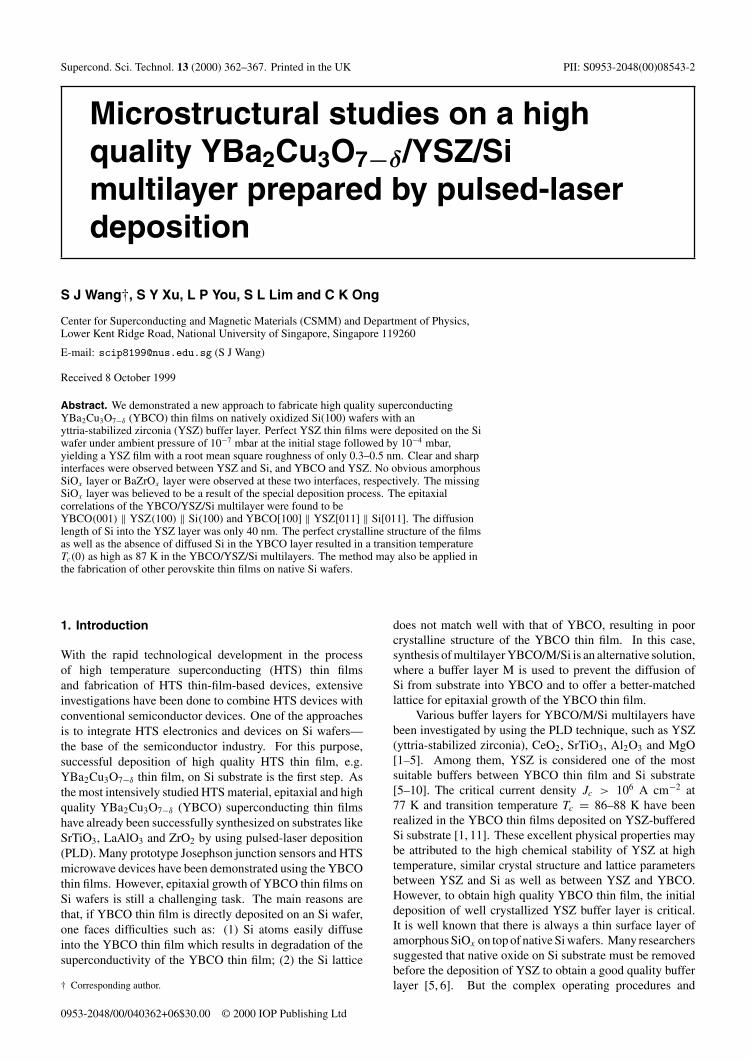
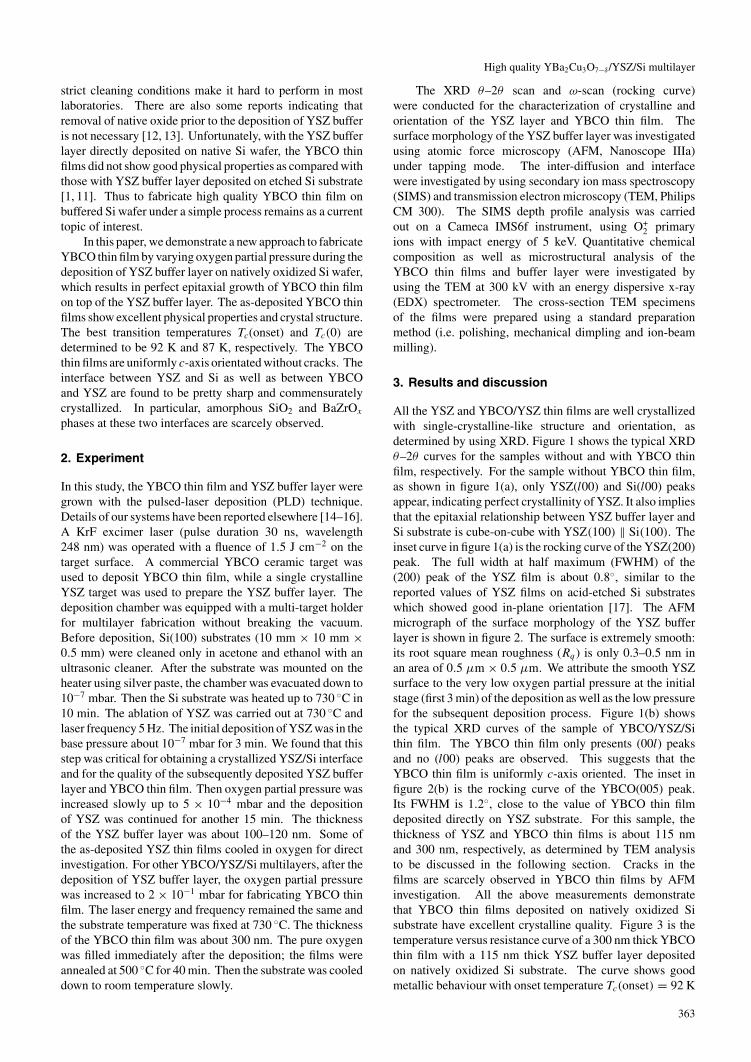
All the YSZ and YBCO/YSZ thin films are well crystallizedwith single-crystalline-like structure and orientation, asdetermined by using XRD. Figure 1 shows the typical XRDθ–2θ curves for the samples without and with YBCO thinfilm, respectively. For the sample without YBCO thin film,as shown in figure 1(a), only YSZ(l00) and Si(l00) peaksappear, indicating perfect crystallinity of YSZ. It also impliesthat the epitaxial relationship between YSZ buffer layer andSi substrate is cube-on-cube with YSZ(100) ‖ Si(100). Theinset curve in figure 1(a) is the rocking curve of the YSZ(200)peak. The full width at half maximum (FWHM) of the(200) peak of the YSZ film is about 0.8◦, similar to thereported values of YSZ films on acid-etched Si substrateswhich showed good in-plane orientation [17]. The AFMmicrograph of the surface morphology of the YSZ bufferlayer is shown in figure 2. The surface is extremely smooth:its root square mean roughness (Rq) is only 0.3–0.5 nm inan area of 0.5 µm × 0.5 µm. We attribute the smooth YSZsurface to the very low oxygen partial pressure at the initialstage (first 3 min) of the deposition as well as the low pressurefor the subsequent deposition process. Figure 1(b) showsthe typical XRD curves of the sample of YBCO/YSZ/Sithin film. The YBCO thin film only presents (00l) peaksand no (l00) peaks are observed. This suggests that theYBCO thin film is uniformly c-axis oriented. The inset infigure 2(b) is the rocking curve of the YBCO(005) peak.Its FWHM is 1.2◦, close to the value of YBCO thin filmdeposited directly on YSZ substrate. For this sample, thethickness of YSZ and YBCO thin films is about 115 nmand 300 nm, respectively, as determined by TEM analysisto be discussed in the following section. Cracks in thefilms are scarcely observed in YBCO thin films by AFMinvestigation. All the above measurements demonstratethat YBCO thin films deposited on natively oxidized Sisubstrate have excellent crystalline quality. Figure 3 is thetemperature versus resistance curve of a 300 nm thick YBCOthin film with a 115 nm thick YSZ buffer layer depositedon natively oxidized Si substrate. The curve shows goodmetallic behaviour with onset temperature Tc(onset) = 92 K
363
S J Wang et al
(a)
(b)
Figure 1. XRD data of two samples without (a) and with (b)YBCO film. The insets are rocking curves of the YSZ(200) peak(a) and YBCO(005) peak (b).
Figure 2. AFM image of 115 nm YSZ buffer deposited onnatively oxidized Si wafer.
and zero resistance temperature Tc(0) = 87 K, indicatinggood transition properties.
A crucial problem of fabricating YBCO thin film onSi substrate is the interfacial inter-diffusion between Si andYBCO. Very little Si diffused into the YBCO thin film will
Figure 3. Resistance versus temperature curve for 300 nm YBCOthin film on natively oxidized Si substrate with 115 nm YSZ bufferlayer.
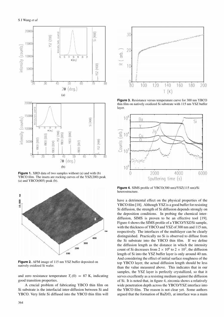
Figure 4. SIMS profile of YBCO(300 nm)/YSZ(115 nm)/Siheterostructure.
have a detrimental effect on the physical properties of theYBCO film [18]. Although YSZ is a good buffer for resistingSi diffusion, the strength of Si diffusion depends strongly onthe deposition conditions. In probing the chemical inter-diffusion, SIMS is proven to be an effective tool [19].Figure 4 shows the SIMS profile of a YBCO/YSZ/Si sample,with the thickness of YBCO and YSZ of 300 nm and 115 nm,respectively. The interfaces of the multilayer can be clearlydistinguished. Practically no Si is observed to diffuse fromthe Si substrate into the YBCO thin film. If we definethe diffusion length as the distance in which the intensitycount of Si decreases from 2 × 10⁶ to 2 × 10³, the diffusionlength of Si into the YSZ buffer layer is only around 40 nm.And considering the effect of initial surface roughness of thetop YBCO layer, the actual diffusion length should be lessthan the value measured above. This indicates that in oursamples, the YSZ layer is perfectly crystallized, so that itserves excellently as a resisting medium against the diffusionof Si. It is noted that, in figure 4, zirconia shows a relativelywide penetration depth across the YBCO/YSZ interface intothe YBCO film. The reason is not clear yet. Some authorsargued that the formation of BaZrOx at interface was a main
364
High quality YBa2Cu3O7−δ/YSZ/Si multilayer
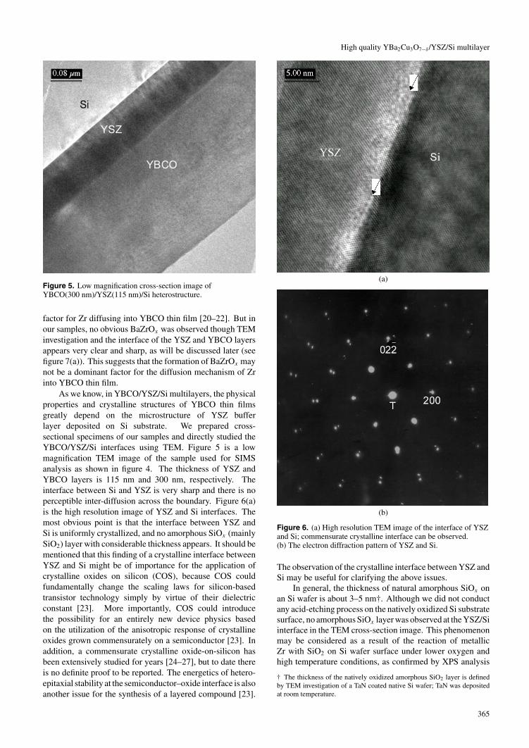
Figure 5. Low magnification cross-section image ofYBCO(300 nm)/YSZ(115 nm)/Si heterostructure.
factor for Zr diffusing into YBCO thin film [20–22]. But inour samples, no obvious BaZrOx was observed though TEMinvestigation and the interface of the YSZ and YBCO layersappears very clear and sharp, as will be discussed later (seefigure 7(a)). This suggests that the formation of BaZrOx maynot be a dominant factor for the diffusion mechanism of Zrinto YBCO thin film.
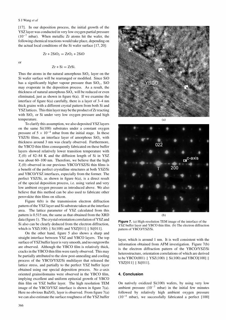
As we know, in YBCO/YSZ/Si multilayers, the physicalproperties and crystalline structures of YBCO thin filmsgreatly depend on the microstructure of YSZ bufferlayer deposited on Si substrate. We prepared cross-sectional specimens of our samples and directly studied theYBCO/YSZ/Si interfaces using TEM. Figure 5 is a lowmagnification TEM image of the sample used for SIMSanalysis as shown in figure 4. The thickness of YSZ andYBCO layers is 115 nm and 300 nm, respectively. Theinterface between Si and YSZ is very sharp and there is noperceptible inter-diffusion across the boundary. Figure 6(a)is the high resolution image of YSZ and Si interfaces. Themost obvious point is that the interface between YSZ andSi is uniformly crystallized, and no amorphous SiOx (mainlySiO2) layer with considerable thickness appears. It should bementioned that this finding of a crystalline interface betweenYSZ and Si might be of importance for the application ofcrystalline oxides on silicon (COS), because COS couldfundamentally change the scaling laws for silicon-basedtransistor technology simply by virtue of their dielectricconstant [23]. More importantly, COS could introducethe possibility for an entirely new device physics basedon the utilization of the anisotropic response of crystallineoxides grown commensurately on a semiconductor [23]. Inaddition, a commensurate crystalline oxide-on-silicon hasbeen extensively studied for years [24–27], but to date thereis no definite proof to be reported. The energetics of hetero-epitaxial stability at the semiconductor–oxide interface is alsoanother issue for the synthesis of a layered compound [23].
(a)
(b)
Figure 6. (a) High resolution TEM image of the interface of YSZand Si; commensurate crystalline interface can be observed.(b) The electron diffraction pattern of YSZ and Si.
The observation of the crystalline interface between YSZ andSi may be useful for clarifying the above issues.
In general, the thickness of natural amorphous SiOx onan Si wafer is about 3–5 nm†. Although we did not conductany acid-etching process on the natively oxidized Si substratesurface, no amorphous SiOx layer was observed at the YSZ/Siinterface in the TEM cross-section image. This phenomenonmay be considered as a result of the reaction of metallicZr with SiO2 on Si wafer surface under lower oxygen andhigh temperature conditions, as confirmed by XPS analysis
† The thickness of the natively oxidized amorphous SiO2 layer is definedby TEM investigation of a TaN coated native Si wafer; TaN was depositedat room temperature.
365
S J Wang et al
[17]. In our deposition process, the initial growth of theYSZ layer was conducted in very low oxygen partial pressure(10−7 mbar). When metallic Zr atoms hit the wafer, thefollowing chemical reactions would take place, depending onthe actual local conditions of the Si wafer surface [17, 20]:
Zr + 2SiO2 = ZrO2 + 2SiO
orZr + Si = ZrSi.
Thus the atoms in the natural amorphous SiOx layer on theSi wafer surface will be rearranged or modified. Since SiOhas a significantly higher vapour pressure than SiOx , SiOmay evaporate in the deposition process. As a result, thethickness of natural amorphous SiOx will be reduced or eveneliminated, just as shown in figure 6(a). If we examine theinterface of figure 6(a) carefully, there is a layer of 3–4 nmthick grains with a different crystal pattern from both Si andYSZ lattices. This thin layer may be the product of Zr reactingwith SiOx or Si under very low oxygen pressure and hightemperature.
To clarify this assumption, we also deposited YSZ layerson the same Si(100) substrates under a constant oxygenpressure of 5 × 10⁻⁴ mbar from the initial stage. In theseYSZ/Si films, an interface layer of amorphous SiOx withthickness around 3 nm was clearly observed. Furthermore,the YBCO thin films consequently fabricated on these bufferlayers showed relatively lower transition temperature withTc(0) of 82–84 K and the diffusion length of Si in YSZwas about 60–100 nm. Therefore, we believe that the highTc(0) observed in our previous YBCO/YSZ/Si thin films isa benefit of the perfect crystalline structures at both YSZ/Siand YBCO/YSZ interfaces, especially from the former. Theperfect YSZ/Si, as shown in figure 6(a), is a direct resultof the special deposition process, i.e. using varied and verylow ambient oxygen pressure as introduced above. We alsobelieve that this method can be also used to fabricate otherperovskite thin films on silicon.
Figure 6(b) is the transmission electron diffractionpattern of the YSZ layer and Si substrate taken at the interfacearea. The lattice parameter of YSZ calculated from thispattern is 0.515 nm, the same as that obtained from the XRDdata (figure 1). The crystal orientation correlation of YSZ andSi also can be clearly deduced from the electron diffraction,which is YSZ(100) ‖ Si(100) and YSZ[011] ‖ Si[011].
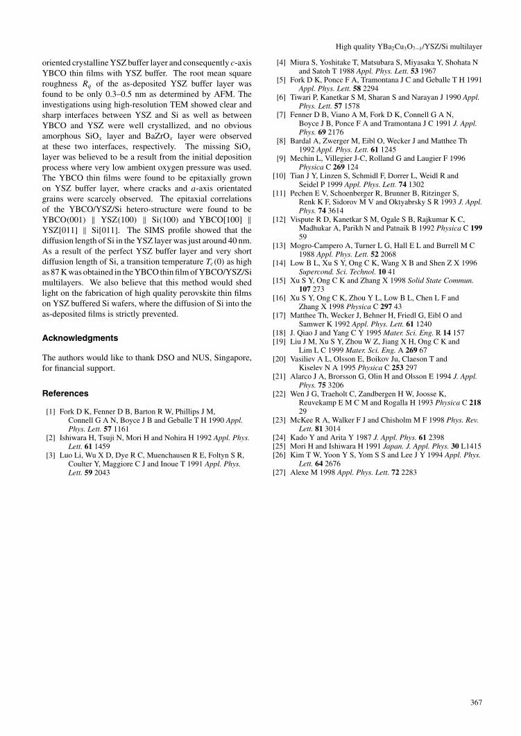
On the other hand, figure 5 also shows a sharp andstraight interface between YSZ and YBCO layers. The topsurface of YSZ buffer layer is very smooth, and no outgrowthsare observed. Although the YBCO film is relatively thick,cracks in the YBCO thin film were rarely observed. This maybe partially attributed to the slow post-annealing and coolingprocess of the YBCO/YSZ/Si multilayer that released thelattice stress, and partially to the perfect YSZ buffer layerobtained using our special deposition process. No a-axisoriented grains/domains were observed in the YBCO film,implying excellent and uniform epitaxial growth of YBCOthin film on YSZ buffer layer. The high resolution TEMimage of the YBCO/YSZ interface is shown in figure 7(a).Here no obvious BaZrOx layer is observed. From figure 7(a)we can also estimate the surface roughness of the YSZ buffer
(a)
(b)
Figure 7. (a) High-resolution TEM image of the interface of theYSZ buffer layer and YBCO thin film. (b) The electron diffractionpattern of YBCO/YSZ/Si.
layer, which is around 1 nm. It is well consistent with theinformation obtained from AFM investigation. Figure 7(b)is the electron diffraction pattern of the YBCO/YSZ/Siheterostructure, orientation correlations of which are derivedto be YBCO(001) ‖ YSZ(100) ‖ Si(100) and YBCO[100] ‖YSZ[011] ‖ Si[011].
4. Conclusion
On natively oxidized Si(100) wafers, by using very lowambient pressure (10−7 mbar) in the initial few minutesfollowed by relatively high ambient oxygen pressure(10−4 mbar), we successfully fabricated a perfect [100]
366
High quality YBa2Cu3O7−δ/YSZ/Si multilayer
oriented crystalline YSZ buffer layer and consequently c-axisYBCO thin films with YSZ buffer. The root mean squareroughness Rq of the as-deposited YSZ buffer layer wasfound to be only 0.3–0.5 nm as determined by AFM. Theinvestigations using high-resolution TEM showed clear andsharp interfaces between YSZ and Si as well as betweenYBCO and YSZ were well crystallized, and no obviousamorphous SiOx layer and BaZrOx layer were observedat these two interfaces, respectively. The missing SiOx
layer was believed to be a result from the initial depositionprocess where very low ambient oxygen pressure was used.The YBCO thin films were found to be epitaxially grownon YSZ buffer layer, where cracks and a-axis orientatedgrains were scarcely observed. The epitaxial correlationsof the YBCO/YSZ/Si hetero-structure were found to beYBCO(001) ‖ YSZ(100) ‖ Si(100) and YBCO[100] ‖YSZ[011] ‖ Si[011]. The SIMS profile showed that thediffusion length of Si in the YSZ layer was just around 40 nm.As a result of the perfect YSZ buffer layer and very shortdiffusion length of Si, a transition temperature Tc(0) as highas 87 K was obtained in the YBCO thin film of YBCO/YSZ/Simultilayers. We also believe that this method would shedlight on the fabrication of high quality perovskite thin filmson YSZ buffered Si wafers, where the diffusion of Si into theas-deposited films is strictly prevented.
Acknowledgments
The authors would like to thank DSO and NUS, Singapore,for financial support.
References
[1] Fork D K, Fenner D B, Barton R W, Phillips J M,Connell G A N, Boyce J B and Geballe T H 1990 Appl.Phys. Lett. 57 1161
[2] Ishiwara H, Tsuji N, Mori H and Nohira H 1992 Appl. Phys.Lett. 61 1459
[3] Luo Li, Wu X D, Dye R C, Muenchausen R E, Foltyn S R,Coulter Y, Maggiore C J and Inoue T 1991 Appl. Phys.Lett. 59 2043
[4] Miura S, Yoshitake T, Matsubara S, Miyasaka Y, Shohata Nand Satoh T 1988 Appl. Phys. Lett. 53 1967
[5] Fork D K, Ponce F A, Tramontana J C and Geballe T H 1991Appl. Phys. Lett. 58 2294
[6] Tiwari P, Kanetkar S M, Sharan S and Narayan J 1990 Appl.Phys. Lett. 57 1578
[7] Fenner D B, Viano A M, Fork D K, Connell G A N,Boyce J B, Ponce F A and Tramontana J C 1991 J. Appl.Phys. 69 2176
[8] Bardal A, Zwerger M, Eibl O, Wecker J and Matthee Th1992 Appl. Phys. Lett. 61 1245
[9] Mechin L, Villegier J-C, Rolland G and Laugier F 1996Physica C 269 124
[10] Tian J Y, Linzen S, Schmidl F, Dorrer L, Weidl R andSeidel P 1999 Appl. Phys. Lett. 74 1302
[11] Pechen E V, Schoenberger R, Brunner B, Ritzinger S,Renk K F, Sidorov M V and Oktyabrsky S R 1993 J. Appl.Phys. 74 3614
[12] Vispute R D, Kanetkar S M, Ogale S B, Rajkumar K C,Madhukar A, Parikh N and Patnaik B 1992 Physica C 19959
[13] Mogro-Campero A, Turner L G, Hall E L and Burrell M C1988 Appl. Phys. Lett. 52 2068
[14] Low B L, Xu S Y, Ong C K, Wang X B and Shen Z X 1996Supercond. Sci. Technol. 10 41
[15] Xu S Y, Ong C K and Zhang X 1998 Solid State Commun.107 273
[16] Xu S Y, Ong C K, Zhou Y L, Low B L, Chen L F andZhang X 1998 Physica C 297 43
[17] Matthee Th, Wecker J, Behner H, Friedl G, Eibl O andSamwer K 1992 Appl. Phys. Lett. 61 1240
[18] J. Qiao J and Yang C Y 1995 Mater. Sci. Eng. R 14 157[19] Liu J M, Xu S Y, Zhou W Z, Jiang X H, Ong C K and
Lim L C 1999 Mater. Sci. Eng. A 269 67[20] Vasiliev A L, Olsson E, Boikov Ju, Claeson T and
Kiselev N A 1995 Physica C 253 297[21] Alarco J A, Brorsson G, Olin H and Olsson E 1994 J. Appl.
Phys. 75 3206[22] Wen J G, Traeholt C, Zandbergen H W, Joosse K,
Reuvekamp E M C M and Rogalla H 1993 Physica C 21829
[23] McKee R A, Walker F J and Chisholm M F 1998 Phys. Rev.Lett. 81 3014
[24] Kado Y and Arita Y 1987 J. Appl. Phys. 61 2398[25] Mori H and Ishiwara H 1991 Japan. J. Appl. Phys. 30 L1415[26] Kim T W, Yoon Y S, Yom S S and Lee J Y 1994 Appl. Phys.
Lett. 64 2676[27] Alexe M 1998 Appl. Phys. Lett. 72 2283
367


![Evaluation of Mechanical and Microstructural Properties of ...€¦ · hardware and architectural frames [5]. ... equipment or miniaturization [4]. An effect of brass alloy part with](https://static.fdocument.org/doc/165x107/605f9ffff279787c4a0be166/evaluation-of-mechanical-and-microstructural-properties-of-hardware-and-architectural.jpg)