MAX925MAX929 .12Gbps GMSL Serialiers or Coax or STP Otpt ... · 56-pin, 8mm x 8mm, TQFN package...
69
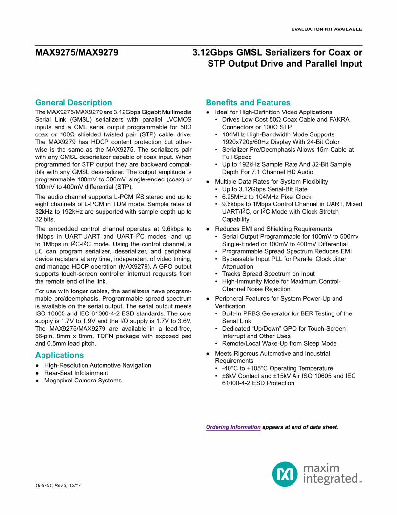
General Description The MAX9275/MAX9279 are 3.12Gbps Gigabit Multimedia Serial Link (GMSL) serializers with parallel LVCMOS inputs and a CML serial output programmable for 50Ω coax or 100Ω shielded twisted pair (STP) cable drive. The MAX9279 has HDCP content protection but other- wise is the same as the MAX9275. The serializers pair with any GMSL deserializer capable of coax input. When programmed for STP output they are backward compat- ible with any GMSL deserializer. The output amplitude is programmable 100mV to 500mV, single-ended (coax) or 100mV to 400mV differential (STP). The audio channel supports L-PCM I 2 S stereo and up to eight channels of L-PCM in TDM mode. Sample rates of 32kHz to 192kHz are supported with sample depth up to 32 bits. The embedded control channel operates at 9.6kbps to 1Mbps in UART-UART and UART-I 2 C modes, and up to 1Mbps in I 2 C-I 2 C mode. Using the control channel, a µC can program serializer, deserializer, and peripheral device registers at any time, independent of video timing, and manage HDCP operation (MAX9279). A GPO output supports touch-screen controller interrupt requests from the remote end of the link. For use with longer cables, the serializers have program- mable pre/deemphasis. Programmable spread spectrum is available on the serial output. The serial output meets ISO 10605 and IEC 61000-4-2 ESD standards. The core supply is 1.7V to 1.9V and the I/O supply is 1.7V to 3.6V. The MAX9275/MAX9279 are available in a lead-free, 56-pin, 8mm x 8mm, TQFN package with exposed pad and 0.5mm lead pitch. Applications ● High-Resolution Automotive Navigation ● Rear-Seat Infotainment ● Megapixel Camera Systems Benefits and Features ● Ideal for High-Definition Video Applications • Drives Low-Cost 50Ω Coax Cable and FAKRA Connectors or 100Ω STP • 104MHz High-Bandwidth Mode Supports 1920x720p/60Hz Display With 24-Bit Color • Serializer Pre/Deemphasis Allows 15m Cable at Full Speed • Up to 192kHz Sample Rate And 32-Bit Sample Depth For 7.1 Channel HD Audio ● Multiple Data Rates for System Flexibility • Up to 3.12Gbps Serial-Bit Rate • 6.25MHz to 104MHz Pixel Clock • 9.6kbps to 1Mbps Control Channel in UART, Mixed UART/I 2 C, or I 2 C Mode with Clock Stretch Capability ● Reduces EMI and Shielding Requirements • Serial Output Programmable for 100mV to 500mv Single-Ended or 100mV to 400mV Differential • Programmable Spread Spectrum Reduces EMI • Bypassable Input PLL for Parallel Clock Jitter Attenuation • Tracks Spread Spectrum on Input • High-Immunity Mode for Maximum Control- Channel Noise Rejection ● Peripheral Features for System Power-Up and Verification • Built-In PRBS Generator for BER Testing of the Serial Link • Dedicated “Up/Down” GPO for Touch-Screen Interrupt and Other Uses • Remote/Local Wake-Up from Sleep Mode ● Meets Rigorous Automotive and Industrial Requirements • -40°C to +105°C Operating Temperature • ±8kV Contact and ±15kV Air ISO 10605 and IEC 61000-4-2 ESD Protection 19-6751; Rev 3; 12/17 Ordering Information appears at end of data sheet. MAX9275/MAX9279 3.12Gbps GMSL Serializers for Coax or STP Output Drive and Parallel Input EVALUATION KIT AVAILABLE
-
Upload
vuongduong -
Category
Documents
-
view
222 -
download
0
Transcript of MAX925MAX929 .12Gbps GMSL Serialiers or Coax or STP Otpt ... · 56-pin, 8mm x 8mm, TQFN package...
General DescriptionThe MAX9275/MAX9279 are 3.12Gbps Gigabit Multimedia Serial Link (GMSL) serializers with parallel LVCMOS inputs and a CML serial output programmable for 50Ω coax or 100Ω shielded twisted pair (STP) cable drive. The MAX9279 has HDCP content protection but other-wise is the same as the MAX9275. The serializers pair with any GMSL deserializer capable of coax input. When programmed for STP output they are backward compat-ible with any GMSL deserializer. The output amplitude is programmable 100mV to 500mV, single-ended (coax) or 100mV to 400mV differential (STP).The audio channel supports L-PCM I2S stereo and up to eight channels of L-PCM in TDM mode. Sample rates of 32kHz to 192kHz are supported with sample depth up to 32 bits.The embedded control channel operates at 9.6kbps to 1Mbps in UART-UART and UART-I2C modes, and up to 1Mbps in I2C-I2C mode. Using the control channel, a µC can program serializer, deserializer, and peripheral device registers at any time, independent of video timing, and manage HDCP operation (MAX9279). A GPO output supports touch-screen controller interrupt requests from the remote end of the link.For use with longer cables, the serializers have program-mable pre/deemphasis. Programmable spread spectrum is available on the serial output. The serial output meets ISO 10605 and IEC 61000-4-2 ESD standards. The core supply is 1.7V to 1.9V and the I/O supply is 1.7V to 3.6V. The MAX9275/MAX9279 are available in a lead-free, 56-pin, 8mm x 8mm, TQFN package with exposed pad and 0.5mm lead pitch.
Applications High-Resolution Automotive Navigation Rear-Seat Infotainment Megapixel Camera Systems
Benefits and Features Ideal for High-Definition Video Applications
• Drives Low-Cost 50Ω Coax Cable and FAKRA Connectors or 100Ω STP • 104MHz High-Bandwidth Mode Supports 1920x720p/60Hz Display With 24-Bit Color • Serializer Pre/Deemphasis Allows 15m Cable at Full Speed • Up to 192kHz Sample Rate And 32-Bit Sample Depth For 7.1 Channel HD Audio
Multiple Data Rates for System Flexibility • Up to 3.12Gbps Serial-Bit Rate • 6.25MHz to 104MHz Pixel Clock • 9.6kbps to 1Mbps Control Channel in UART, Mixed UART/I2C, or I2C Mode with Clock Stretch Capability
Reduces EMI and Shielding Requirements • Serial Output Programmable for 100mV to 500mv Single-Ended or 100mV to 400mV Differential • Programmable Spread Spectrum Reduces EMI • Bypassable Input PLL for Parallel Clock Jitter Attenuation • Tracks Spread Spectrum on Input • High-Immunity Mode for Maximum Control- Channel Noise Rejection
Peripheral Features for System Power-Up and Verification • Built-In PRBS Generator for BER Testing of the Serial Link • Dedicated “Up/Down” GPO for Touch-Screen Interrupt and Other Uses • Remote/Local Wake-Up from Sleep Mode
Meets Rigorous Automotive and Industrial Requirements • -40°C to +105°C Operating Temperature • ±8kV Contact and ±15kV Air ISO 10605 and IEC 61000-4-2 ESD Protection
19-6751; Rev 3; 12/17
Ordering Information appears at end of data sheet.
MAX9275/MAX9279 3.12Gbps GMSL Serializers for Coax or STP Output Drive and Parallel Input
EVALUATION KIT AVAILABLE
MAX9275/MAX9279 3.12Gbps GMSL Serializers for Coax or STP Output Drive and Parallel Input
www.maximintegrated.com Maxim Integrated 2
TABLE OF CONTENTS
General Description . . . . . . . . . . . . . . . . . . . . . . . . . . . . . . . . . . . . . . . . . . . . . . . . . . . . . . . . . . . . . . . . . . . . . . . . . . . . 1Benefits and Features . . . . . . . . . . . . . . . . . . . . . . . . . . . . . . . . . . . . . . . . . . . . . . . . . . . . . . . . . . . . . . . . . . . . . . . . . . 1Absolute Maximum Ratings . . . . . . . . . . . . . . . . . . . . . . . . . . . . . . . . . . . . . . . . . . . . . . . . . . . . . . . . . . . . . . . . . . . . . . 7Package Thermal Characteristics . . . . . . . . . . . . . . . . . . . . . . . . . . . . . . . . . . . . . . . . . . . . . . . . . . . . . . . . . . . . . . . . . 7DC Electrical Characteristics . . . . . . . . . . . . . . . . . . . . . . . . . . . . . . . . . . . . . . . . . . . . . . . . . . . . . . . . . . . . . . . . . . . . . 7AC Electrical Characteristics . . . . . . . . . . . . . . . . . . . . . . . . . . . . . . . . . . . . . . . . . . . . . . . . . . . . . . . . . . . . . . . . . . . . 10Typical Operating Characteristics . . . . . . . . . . . . . . . . . . . . . . . . . . . . . . . . . . . . . . . . . . . . . . . . . . . . . . . . . . . . . . . . 13Pin Configuration . . . . . . . . . . . . . . . . . . . . . . . . . . . . . . . . . . . . . . . . . . . . . . . . . . . . . . . . . . . . . . . . . . . . . . . . . . . . . 15Pin Description . . . . . . . . . . . . . . . . . . . . . . . . . . . . . . . . . . . . . . . . . . . . . . . . . . . . . . . . . . . . . . . . . . . . . . . . . . . . . . . 15Functional Diagram . . . . . . . . . . . . . . . . . . . . . . . . . . . . . . . . . . . . . . . . . . . . . . . . . . . . . . . . . . . . . . . . . . . . . . . . . . . 18Detailed Description. . . . . . . . . . . . . . . . . . . . . . . . . . . . . . . . . . . . . . . . . . . . . . . . . . . . . . . . . . . . . . . . . . . . . . . . . . . 25
Register Mapping . . . . . . . . . . . . . . . . . . . . . . . . . . . . . . . . . . . . . . . . . . . . . . . . . . . . . . . . . . . . . . . . . . . . . . . . . . . 25Serial Link Signaling and Data Format . . . . . . . . . . . . . . . . . . . . . . . . . . . . . . . . . . . . . . . . . . . . . . . . . . . . . . . . . . . 26Data-Rate Selection . . . . . . . . . . . . . . . . . . . . . . . . . . . . . . . . . . . . . . . . . . . . . . . . . . . . . . . . . . . . . . . . . . . . . . . . . 26High-Bandwidth Mode . . . . . . . . . . . . . . . . . . . . . . . . . . . . . . . . . . . . . . . . . . . . . . . . . . . . . . . . . . . . . . . . . . . . . . . 26Audio Channel. . . . . . . . . . . . . . . . . . . . . . . . . . . . . . . . . . . . . . . . . . . . . . . . . . . . . . . . . . . . . . . . . . . . . . . . . . . . . . 28
Audio Channel Input . . . . . . . . . . . . . . . . . . . . . . . . . . . . . . . . . . . . . . . . . . . . . . . . . . . . . . . . . . . . . . . . . . . . . . 29Reverse Control Channel . . . . . . . . . . . . . . . . . . . . . . . . . . . . . . . . . . . . . . . . . . . . . . . . . . . . . . . . . . . . . . . . . . . . . 30Control Channel and Register Programming . . . . . . . . . . . . . . . . . . . . . . . . . . . . . . . . . . . . . . . . . . . . . . . . . . . . . . 30
UART Interface . . . . . . . . . . . . . . . . . . . . . . . . . . . . . . . . . . . . . . . . . . . . . . . . . . . . . . . . . . . . . . . . . . . . . . . . . . 30Interfacing Command-Byte-Only I2C Devices with UART . . . . . . . . . . . . . . . . . . . . . . . . . . . . . . . . . . . . . . . . . 32UART Bypass Mode . . . . . . . . . . . . . . . . . . . . . . . . . . . . . . . . . . . . . . . . . . . . . . . . . . . . . . . . . . . . . . . . . . . . . . 32
I2C Interface . . . . . . . . . . . . . . . . . . . . . . . . . . . . . . . . . . . . . . . . . . . . . . . . . . . . . . . . . . . . . . . . . . . . . . . . . . . . . . . 33START and STOP Conditions . . . . . . . . . . . . . . . . . . . . . . . . . . . . . . . . . . . . . . . . . . . . . . . . . . . . . . . . . . . . . . . 34Bit Transfer. . . . . . . . . . . . . . . . . . . . . . . . . . . . . . . . . . . . . . . . . . . . . . . . . . . . . . . . . . . . . . . . . . . . . . . . . . . . . . 34Acknowledge . . . . . . . . . . . . . . . . . . . . . . . . . . . . . . . . . . . . . . . . . . . . . . . . . . . . . . . . . . . . . . . . . . . . . . . . . . . . 35Slave Address . . . . . . . . . . . . . . . . . . . . . . . . . . . . . . . . . . . . . . . . . . . . . . . . . . . . . . . . . . . . . . . . . . . . . . . . . . . 35Bus Reset. . . . . . . . . . . . . . . . . . . . . . . . . . . . . . . . . . . . . . . . . . . . . . . . . . . . . . . . . . . . . . . . . . . . . . . . . . . . . . . 35
Format for Writing . . . . . . . . . . . . . . . . . . . . . . . . . . . . . . . . . . . . . . . . . . . . . . . . . . . . . . . . . . . . . . . . . . . . . . . . . . . 35Format for Reading . . . . . . . . . . . . . . . . . . . . . . . . . . . . . . . . . . . . . . . . . . . . . . . . . . . . . . . . . . . . . . . . . . . . . . . 36I2C Communication with Remote Side Devices . . . . . . . . . . . . . . . . . . . . . . . . . . . . . . . . . . . . . . . . . . . . . . . . . 36
I2C Address Translation . . . . . . . . . . . . . . . . . . . . . . . . . . . . . . . . . . . . . . . . . . . . . . . . . . . . . . . . . . . . . . . . . . . . . . 36GPO/GPI Control . . . . . . . . . . . . . . . . . . . . . . . . . . . . . . . . . . . . . . . . . . . . . . . . . . . . . . . . . . . . . . . . . . . . . . . . . . . 37Pre/Deemphasis Driver . . . . . . . . . . . . . . . . . . . . . . . . . . . . . . . . . . . . . . . . . . . . . . . . . . . . . . . . . . . . . . . . . . . . . . . 37Spread Spectrum . . . . . . . . . . . . . . . . . . . . . . . . . . . . . . . . . . . . . . . . . . . . . . . . . . . . . . . . . . . . . . . . . . . . . . . . . . . 37Manual Programming of the Spread-Spectrum Divider . . . . . . . . . . . . . . . . . . . . . . . . . . . . . . . . . . . . . . . . . . . . . . 39Serial Output . . . . . . . . . . . . . . . . . . . . . . . . . . . . . . . . . . . . . . . . . . . . . . . . . . . . . . . . . . . . . . . . . . . . . . . . . . . . . . . 39
MAX9275/MAX9279 3.12Gbps GMSL Serializers for Coax or STP Output Drive and Parallel Input
www.maximintegrated.com Maxim Integrated 3
TABLE OF CONTENTS (continued)
Coax Splitter Mode . . . . . . . . . . . . . . . . . . . . . . . . . . . . . . . . . . . . . . . . . . . . . . . . . . . . . . . . . . . . . . . . . . . . . . . . . . 39High-Immunity Reverse Control Channel Mode . . . . . . . . . . . . . . . . . . . . . . . . . . . . . . . . . . . . . . . . . . . . . . . . . . . . 40Sleep Mode . . . . . . . . . . . . . . . . . . . . . . . . . . . . . . . . . . . . . . . . . . . . . . . . . . . . . . . . . . . . . . . . . . . . . . . . . . . . . . . . 41Power-Down Mode . . . . . . . . . . . . . . . . . . . . . . . . . . . . . . . . . . . . . . . . . . . . . . . . . . . . . . . . . . . . . . . . . . . . . . . . . . 41Configuration Link . . . . . . . . . . . . . . . . . . . . . . . . . . . . . . . . . . . . . . . . . . . . . . . . . . . . . . . . . . . . . . . . . . . . . . . . . . . 41
Link Startup Procedure . . . . . . . . . . . . . . . . . . . . . . . . . . . . . . . . . . . . . . . . . . . . . . . . . . . . . . . . . . . . . . . . . . . . . . . . 42Encryption Enable . . . . . . . . . . . . . . . . . . . . . . . . . . . . . . . . . . . . . . . . . . . . . . . . . . . . . . . . . . . . . . . . . . . . . . . . . . . 45Synchronization of Encryption . . . . . . . . . . . . . . . . . . . . . . . . . . . . . . . . . . . . . . . . . . . . . . . . . . . . . . . . . . . . . . . . . 45Repeater Support . . . . . . . . . . . . . . . . . . . . . . . . . . . . . . . . . . . . . . . . . . . . . . . . . . . . . . . . . . . . . . . . . . . . . . . . . . . 45
HDCP Authentication Procedures . . . . . . . . . . . . . . . . . . . . . . . . . . . . . . . . . . . . . . . . . . . . . . . . . . . . . . . . . . . . . . . . 45HDCP Protocol Summary . . . . . . . . . . . . . . . . . . . . . . . . . . . . . . . . . . . . . . . . . . . . . . . . . . . . . . . . . . . . . . . . . . . . . 46
Example Repeater Network—Two µCs . . . . . . . . . . . . . . . . . . . . . . . . . . . . . . . . . . . . . . . . . . . . . . . . . . . . . . . . 46Detection and Action Upon New Device Connection . . . . . . . . . . . . . . . . . . . . . . . . . . . . . . . . . . . . . . . . . . . . . . . . 46Notification of Start of Authentication and Enable of Encryption to Downstream Links . . . . . . . . . . . . . . . . . . . . . 46
Applications Information. . . . . . . . . . . . . . . . . . . . . . . . . . . . . . . . . . . . . . . . . . . . . . . . . . . . . . . . . . . . . . . . . . . . . . . . 54Self PRBS Test . . . . . . . . . . . . . . . . . . . . . . . . . . . . . . . . . . . . . . . . . . . . . . . . . . . . . . . . . . . . . . . . . . . . . . . . . . . . . 54Dual µC Control . . . . . . . . . . . . . . . . . . . . . . . . . . . . . . . . . . . . . . . . . . . . . . . . . . . . . . . . . . . . . . . . . . . . . . . . . . . . 54PCLKIN Spread Tracking . . . . . . . . . . . . . . . . . . . . . . . . . . . . . . . . . . . . . . . . . . . . . . . . . . . . . . . . . . . . . . . . . . . . . 54Changing the Clock Frequency. . . . . . . . . . . . . . . . . . . . . . . . . . . . . . . . . . . . . . . . . . . . . . . . . . . . . . . . . . . . . . . . . 54Providing a Frame Sync (Camera Applications) . . . . . . . . . . . . . . . . . . . . . . . . . . . . . . . . . . . . . . . . . . . . . . . . . . . . 54Software Programming of the Device Addresses. . . . . . . . . . . . . . . . . . . . . . . . . . . . . . . . . . . . . . . . . . . . . . . . . . . 54Configuration Blocking . . . . . . . . . . . . . . . . . . . . . . . . . . . . . . . . . . . . . . . . . . . . . . . . . . . . . . . . . . . . . . . . . . . . . . . 55Compatibility with Other GMSL Devices . . . . . . . . . . . . . . . . . . . . . . . . . . . . . . . . . . . . . . . . . . . . . . . . . . . . . . . . . 55Key Memory . . . . . . . . . . . . . . . . . . . . . . . . . . . . . . . . . . . . . . . . . . . . . . . . . . . . . . . . . . . . . . . . . . . . . . . . . . . . . . . 55HS/VS/DE Inversion . . . . . . . . . . . . . . . . . . . . . . . . . . . . . . . . . . . . . . . . . . . . . . . . . . . . . . . . . . . . . . . . . . . . . . . . . 55WS/SCK Inversion . . . . . . . . . . . . . . . . . . . . . . . . . . . . . . . . . . . . . . . . . . . . . . . . . . . . . . . . . . . . . . . . . . . . . . . . . . 55Line-Fault Detection . . . . . . . . . . . . . . . . . . . . . . . . . . . . . . . . . . . . . . . . . . . . . . . . . . . . . . . . . . . . . . . . . . . . . . . . . 55Internal Input Pulldowns . . . . . . . . . . . . . . . . . . . . . . . . . . . . . . . . . . . . . . . . . . . . . . . . . . . . . . . . . . . . . . . . . . . . . . 56Choosing I2C/UART Pullup Resistors . . . . . . . . . . . . . . . . . . . . . . . . . . . . . . . . . . . . . . . . . . . . . . . . . . . . . . . . . . . 56AC-Coupling . . . . . . . . . . . . . . . . . . . . . . . . . . . . . . . . . . . . . . . . . . . . . . . . . . . . . . . . . . . . . . . . . . . . . . . . . . . . . . . 56Selection of AC-Coupling Capacitors . . . . . . . . . . . . . . . . . . . . . . . . . . . . . . . . . . . . . . . . . . . . . . . . . . . . . . . . . . . . 56Power-Supply Circuits and Bypassing . . . . . . . . . . . . . . . . . . . . . . . . . . . . . . . . . . . . . . . . . . . . . . . . . . . . . . . . . . . 56Power-Supply Table . . . . . . . . . . . . . . . . . . . . . . . . . . . . . . . . . . . . . . . . . . . . . . . . . . . . . . . . . . . . . . . . . . . . . . . . . 57Cables and Connectors . . . . . . . . . . . . . . . . . . . . . . . . . . . . . . . . . . . . . . . . . . . . . . . . . . . . . . . . . . . . . . . . . . . . . . 57Board Layout. . . . . . . . . . . . . . . . . . . . . . . . . . . . . . . . . . . . . . . . . . . . . . . . . . . . . . . . . . . . . . . . . . . . . . . . . . . . . . . 57
Typical Application Circuit . . . . . . . . . . . . . . . . . . . . . . . . . . . . . . . . . . . . . . . . . . . . . . . . . . . . . . . . . . . . . . . . . . . . . . 68Ordering Information . . . . . . . . . . . . . . . . . . . . . . . . . . . . . . . . . . . . . . . . . . . . . . . . . . . . . . . . . . . . . . . . . . . . . . . . . . 68
MAX9275/MAX9279 3.12Gbps GMSL Serializers for Coax or STP Output Drive and Parallel Input
www.maximintegrated.com Maxim Integrated 4
LIST OF FIGURES
TABLE OF CONTENTS (continued)
Chip Information . . . . . . . . . . . . . . . . . . . . . . . . . . . . . . . . . . . . . . . . . . . . . . . . . . . . . . . . . . . . . . . . . . . . . . . . . . . . . . 68Package Information . . . . . . . . . . . . . . . . . . . . . . . . . . . . . . . . . . . . . . . . . . . . . . . . . . . . . . . . . . . . . . . . . . . . . . . . . . 68Revision History . . . . . . . . . . . . . . . . . . . . . . . . . . . . . . . . . . . . . . . . . . . . . . . . . . . . . . . . . . . . . . . . . . . . . . . . . . . . . . 69
Figure 1. Serial-Output Parameters . . . . . . . . . . . . . . . . . . . . . . . . . . . . . . . . . . . . . . . . . . . . . . . . . . . . . . . . . . . . . . . 19Figure 2. Output Waveforms at OUT+, OUT- . . . . . . . . . . . . . . . . . . . . . . . . . . . . . . . . . . . . . . . . . . . . . . . . . . . . . . . . 19Figure 3. Single-Ended Output Template . . . . . . . . . . . . . . . . . . . . . . . . . . . . . . . . . . . . . . . . . . . . . . . . . . . . . . . . . . 19Figure 4. Line Fault Detector Circuit . . . . . . . . . . . . . . . . . . . . . . . . . . . . . . . . . . . . . . . . . . . . . . . . . . . . . . . . . . . . . . 20Figure 5. Worst-Case Pattern Input . . . . . . . . . . . . . . . . . . . . . . . . . . . . . . . . . . . . . . . . . . . . . . . . . . . . . . . . . . . . . . . 20Figure 6. Parallel Clock Input Requirements . . . . . . . . . . . . . . . . . . . . . . . . . . . . . . . . . . . . . . . . . . . . . . . . . . . . . . . . 21Figure 7. I2C Timing Parameters . . . . . . . . . . . . . . . . . . . . . . . . . . . . . . . . . . . . . . . . . . . . . . . . . . . . . . . . . . . . . . . . . 21Figure 8. Differential Output Template. . . . . . . . . . . . . . . . . . . . . . . . . . . . . . . . . . . . . . . . . . . . . . . . . . . . . . . . . . . . . 21Figure 9. Input Setup and Hold Times . . . . . . . . . . . . . . . . . . . . . . . . . . . . . . . . . . . . . . . . . . . . . . . . . . . . . . . . . . . . . 22Figure 10. GPI-to-GPO Delay . . . . . . . . . . . . . . . . . . . . . . . . . . . . . . . . . . . . . . . . . . . . . . . . . . . . . . . . . . . . . . . . . . . 22Figure 11. Serializer Delay . . . . . . . . . . . . . . . . . . . . . . . . . . . . . . . . . . . . . . . . . . . . . . . . . . . . . . . . . . . . . . . . . . . . . . 23Figure 12. Link Startup Time . . . . . . . . . . . . . . . . . . . . . . . . . . . . . . . . . . . . . . . . . . . . . . . . . . . . . . . . . . . . . . . . . . . . 23Figure 13. Power-Up Delay . . . . . . . . . . . . . . . . . . . . . . . . . . . . . . . . . . . . . . . . . . . . . . . . . . . . . . . . . . . . . . . . . . . . . 24Figure 14. Input I2S Timing Parameters . . . . . . . . . . . . . . . . . . . . . . . . . . . . . . . . . . . . . . . . . . . . . . . . . . . . . . . . . . . 24Figure 15. 24-Bit Mode Serial Data Format. . . . . . . . . . . . . . . . . . . . . . . . . . . . . . . . . . . . . . . . . . . . . . . . . . . . . . . . . 26Figure 16. 32-Bit Mode Serial Data Format . . . . . . . . . . . . . . . . . . . . . . . . . . . . . . . . . . . . . . . . . . . . . . . . . . . . . . . . . 27Figure 17. High-Bandwidth Mode Serial Data Format . . . . . . . . . . . . . . . . . . . . . . . . . . . . . . . . . . . . . . . . . . . . . . . . . 27Figure 18. Audio Channel Input Format . . . . . . . . . . . . . . . . . . . . . . . . . . . . . . . . . . . . . . . . . . . . . . . . . . . . . . . . . . . . 29Figure 19. 8-Channel TDM (24-Bit Samples, Padded with Zeros) . . . . . . . . . . . . . . . . . . . . . . . . . . . . . . . . . . . . . . . 29Figure 20. 6-Channel TDM (24-Bit Samples, No Padding) . . . . . . . . . . . . . . . . . . . . . . . . . . . . . . . . . . . . . . . . . . . . . 29Figure 21. Stereo I2S (24-Bit Samples, Padded with Zeros) . . . . . . . . . . . . . . . . . . . . . . . . . . . . . . . . . . . . . . . . . . . . 30Figure 22. Stereo I2S (16-Bit Samples, No Padding) . . . . . . . . . . . . . . . . . . . . . . . . . . . . . . . . . . . . . . . . . . . . . . . . . 30Figure 23. GMSL UART Protocol for Base Mode . . . . . . . . . . . . . . . . . . . . . . . . . . . . . . . . . . . . . . . . . . . . . . . . . . . . 31Figure 24. GMSL UART Data Format for Base Mode . . . . . . . . . . . . . . . . . . . . . . . . . . . . . . . . . . . . . . . . . . . . . . . . . 31Figure 25. Sync Byte (0x79). . . . . . . . . . . . . . . . . . . . . . . . . . . . . . . . . . . . . . . . . . . . . . . . . . . . . . . . . . . . . . . . . . . . . 31Figure 26. ACK Byte (0xC3). . . . . . . . . . . . . . . . . . . . . . . . . . . . . . . . . . . . . . . . . . . . . . . . . . . . . . . . . . . . . . . . . . . . . 31Figure 27. Format Conversion Between GMSL UART and I2C with Register Address (I2CMETHOD = 0) . . . . . . . . 32Figure 28. Format Conversion Between GMSL UART and I2C without Register Address (I2CMETHOD = 1) . . . . . 33Figure 29. START and STOP Conditions . . . . . . . . . . . . . . . . . . . . . . . . . . . . . . . . . . . . . . . . . . . . . . . . . . . . . . . . . . 34
MAX9275/MAX9279 3.12Gbps GMSL Serializers for Coax or STP Output Drive and Parallel Input
www.maximintegrated.com Maxim Integrated 5
LIST OF FIGURES (continued)
Figure 30. Bit Transfer . . . . . . . . . . . . . . . . . . . . . . . . . . . . . . . . . . . . . . . . . . . . . . . . . . . . . . . . . . . . . . . . . . . . . . . . . 34Figure 31. Acknowledge. . . . . . . . . . . . . . . . . . . . . . . . . . . . . . . . . . . . . . . . . . . . . . . . . . . . . . . . . . . . . . . . . . . . . . . . 35Figure 32. Slave Address . . . . . . . . . . . . . . . . . . . . . . . . . . . . . . . . . . . . . . . . . . . . . . . . . . . . . . . . . . . . . . . . . . . . . . . 35Figure 33. Format for I2C Write . . . . . . . . . . . . . . . . . . . . . . . . . . . . . . . . . . . . . . . . . . . . . . . . . . . . . . . . . . . . . . . . . . 36Figure 34. Format for Write to Multiple Registers . . . . . . . . . . . . . . . . . . . . . . . . . . . . . . . . . . . . . . . . . . . . . . . . . . . . 36Figure 35. Format for I2C Read . . . . . . . . . . . . . . . . . . . . . . . . . . . . . . . . . . . . . . . . . . . . . . . . . . . . . . . . . . . . . . . . . . 37Figure 36. 2:1 Coax Splitter Connection Diagram. . . . . . . . . . . . . . . . . . . . . . . . . . . . . . . . . . . . . . . . . . . . . . . . . . . . 39Figure 37. Coax Connection Diagram . . . . . . . . . . . . . . . . . . . . . . . . . . . . . . . . . . . . . . . . . . . . . . . . . . . . . . . . . . . . . 39Figure 38. State Diagram, CDS = LOW (Video Display Application) . . . . . . . . . . . . . . . . . . . . . . . . . . . . . . . . . . . . . 43Figure 39. State Diagram, CDS = HIGH (Image Sensing Application) . . . . . . . . . . . . . . . . . . . . . . . . . . . . . . . . . . . . 44Figure 40. Example Network with One Repeater and Two µCs (Tx = GMSL Serializer’s, Rx = Deserializer’s). . . . . 50Figure 41. Human Body Model ESD Test Circuit . . . . . . . . . . . . . . . . . . . . . . . . . . . . . . . . . . . . . . . . . . . . . . . . . . . . . 58Figure 42. IEC 61000-4-2 Contact Discharge ESD Test Circuit . . . . . . . . . . . . . . . . . . . . . . . . . . . . . . . . . . . . . . . . . 58Figure 43. ISO 10605 Contact Discharge ESD Test Circuit . . . . . . . . . . . . . . . . . . . . . . . . . . . . . . . . . . . . . . . . . . . . 58
MAX9275/MAX9279 3.12Gbps GMSL Serializers for Coax or STP Output Drive and Parallel Input
www.maximintegrated.com Maxim Integrated 6
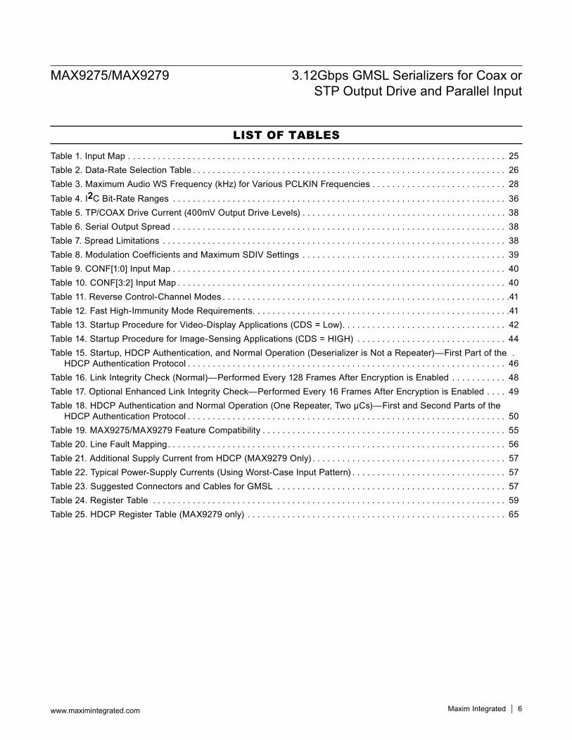
LIST OF TABLES
Table 1. Input Map . . . . . . . . . . . . . . . . . . . . . . . . . . . . . . . . . . . . . . . . . . . . . . . . . . . . . . . . . . . . . . . . . . . . . . . . . . . . 25Table 2. Data-Rate Selection Table . . . . . . . . . . . . . . . . . . . . . . . . . . . . . . . . . . . . . . . . . . . . . . . . . . . . . . . . . . . . . . . 26Table 3. Maximum Audio WS Frequency (kHz) for Various PCLKIN Frequencies . . . . . . . . . . . . . . . . . . . . . . . . . . . 28Table 4. I2C Bit-Rate Ranges . . . . . . . . . . . . . . . . . . . . . . . . . . . . . . . . . . . . . . . . . . . . . . . . . . . . . . . . . . . . . . . . . . . 36Table 5. TP/COAX Drive Current (400mV Output Drive Levels) . . . . . . . . . . . . . . . . . . . . . . . . . . . . . . . . . . . . . . . . . 38Table 6. Serial Output Spread . . . . . . . . . . . . . . . . . . . . . . . . . . . . . . . . . . . . . . . . . . . . . . . . . . . . . . . . . . . . . . . . . . . 38Table 7. Spread Limitations . . . . . . . . . . . . . . . . . . . . . . . . . . . . . . . . . . . . . . . . . . . . . . . . . . . . . . . . . . . . . . . . . . . . . 38Table 8. Modulation Coefficients and Maximum SDIV Settings . . . . . . . . . . . . . . . . . . . . . . . . . . . . . . . . . . . . . . . . . 39Table 9. CONF[1:0] Input Map . . . . . . . . . . . . . . . . . . . . . . . . . . . . . . . . . . . . . . . . . . . . . . . . . . . . . . . . . . . . . . . . . . . 40Table 10. CONF[3:2] Input Map . . . . . . . . . . . . . . . . . . . . . . . . . . . . . . . . . . . . . . . . . . . . . . . . . . . . . . . . . . . . . . . . . . 40Table 11. Reverse Control-Channel Modes . . . . . . . . . . . . . . . . . . . . . . . . . . . . . . . . . . . . . . . . . . . . . . . . . . . . . . . . . .41Table 12. Fast High-Immunity Mode Requirements. . . . . . . . . . . . . . . . . . . . . . . . . . . . . . . . . . . . . . . . . . . . . . . . . . . .41Table 13. Startup Procedure for Video-Display Applications (CDS = Low). . . . . . . . . . . . . . . . . . . . . . . . . . . . . . . . . 42Table 14. Startup Procedure for Image-Sensing Applications (CDS = HIGH) . . . . . . . . . . . . . . . . . . . . . . . . . . . . . . 44Table 15. Startup, HDCP Authentication, and Normal Operation (Deserializer is Not a Repeater)—First Part of the . HDCP Authentication Protocol . . . . . . . . . . . . . . . . . . . . . . . . . . . . . . . . . . . . . . . . . . . . . . . . . . . . . . . . . . . . . . . . 46Table 16. Link Integrity Check (Normal)—Performed Every 128 Frames After Encryption is Enabled . . . . . . . . . . . 48Table 17. Optional Enhanced Link Integrity Check—Performed Every 16 Frames After Encryption is Enabled . . . . 49Table 18. HDCP Authentication and Normal Operation (One Repeater, Two µCs)—First and Second Parts of the HDCP Authentication Protocol . . . . . . . . . . . . . . . . . . . . . . . . . . . . . . . . . . . . . . . . . . . . . . . . . . . . . . . . . . . . . . . . 50Table 19. MAX9275/MAX9279 Feature Compatibility . . . . . . . . . . . . . . . . . . . . . . . . . . . . . . . . . . . . . . . . . . . . . . . . . 55Table 20. Line Fault Mapping. . . . . . . . . . . . . . . . . . . . . . . . . . . . . . . . . . . . . . . . . . . . . . . . . . . . . . . . . . . . . . . . . . . . 56Table 21. Additional Supply Current from HDCP (MAX9279 Only) . . . . . . . . . . . . . . . . . . . . . . . . . . . . . . . . . . . . . . . 57Table 22. Typical Power-Supply Currents (Using Worst-Case Input Pattern) . . . . . . . . . . . . . . . . . . . . . . . . . . . . . . . 57Table 23. Suggested Connectors and Cables for GMSL . . . . . . . . . . . . . . . . . . . . . . . . . . . . . . . . . . . . . . . . . . . . . . 57Table 24. Register Table . . . . . . . . . . . . . . . . . . . . . . . . . . . . . . . . . . . . . . . . . . . . . . . . . . . . . . . . . . . . . . . . . . . . . . . 59Table 25. HDCP Register Table (MAX9279 only) . . . . . . . . . . . . . . . . . . . . . . . . . . . . . . . . . . . . . . . . . . . . . . . . . . . . 65
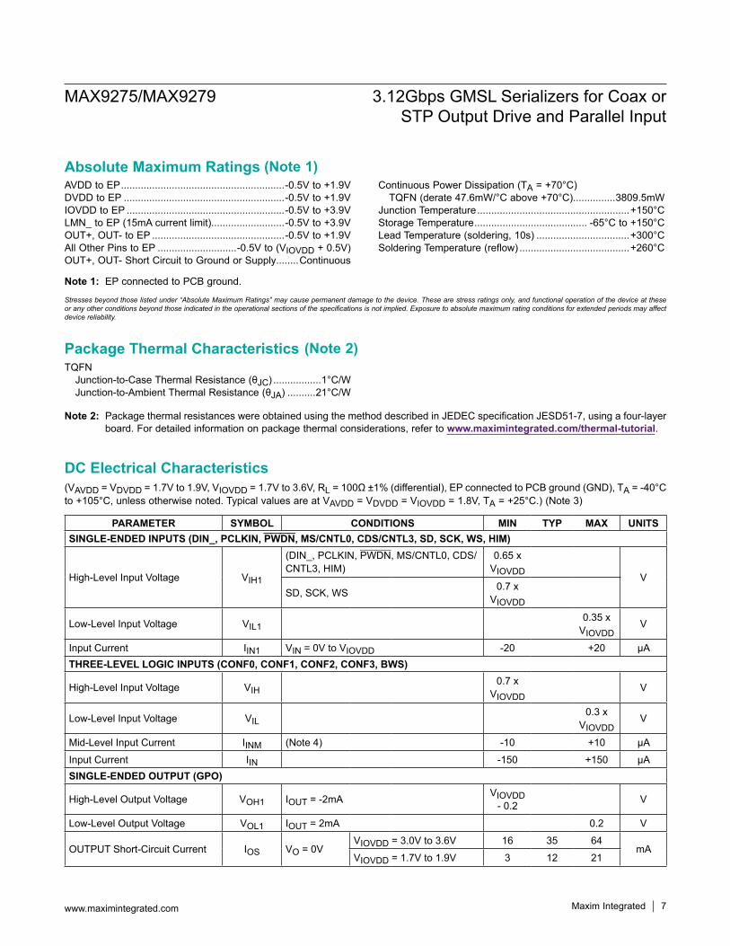
AVDD to EP ..........................................................-0.5V to +1.9VDVDD to EP .........................................................-0.5V to +1.9VIOVDD to EP ........................................................-0.5V to +3.9VLMN_ to EP (15mA current limit)..........................-0.5V to +3.9VOUT+, OUT- to EP ...............................................-0.5V to +1.9VAll Other Pins to EP ............................-0.5V to (VIOVDD + 0.5V)OUT+, OUT- Short Circuit to Ground or Supply........Continuous
Continuous Power Dissipation (TA = +70°C) TQFN (derate 47.6mW/°C above +70°C)...............3809.5mW
Junction Temperature ......................................................+150°CStorage Temperature ........................................ -65°C to +150°CLead Temperature (soldering, 10s) .................................+300°CSoldering Temperature (reflow) .......................................+260°C
TQFN Junction-to-Case Thermal Resistance (θJC) .................1°C/W Junction-to-Ambient Thermal Resistance (θJA) ..........21°C/W
Note 2: Package thermal resistances were obtained using the method described in JEDEC specification JESD51-7, using a four-layer board. For detailed information on package thermal considerations, refer to www.maximintegrated.com/thermal-tutorial.
(VAVDD = VDVDD = 1.7V to 1.9V, VIOVDD = 1.7V to 3.6V, RL = 100Ω ±1% (differential), EP connected to PCB ground (GND), TA = -40°C to +105°C, unless otherwise noted. Typical values are at VAVDD = VDVDD = VIOVDD = 1.8V, TA = +25°C.) (Note 3)
MAX9275/MAX9279 3.12Gbps GMSL Serializers for Coax or STP Output Drive and Parallel Input
www.maximintegrated.com Maxim Integrated 7
Note 1: EP connected to PCB ground.
PARAMETER SYMBOL CONDITIONS MIN TYP MAX UNITSSINGLE-ENDED INPUTS (DIN_, PCLKIN, PWDN, MS/CNTL0, CDS/CNTL3, SD, SCK, WS, HIM)
High-Level Input Voltage VIH1
(DIN_, PCLKIN, PWDN, MS/CNTL0, CDS/CNTL3, HIM)
0.65 xVIOVDD V
SD, SCK, WS 0.7 x VIOVDD
Low-Level Input Voltage VIL10.35 x
VIOVDDV
Input Current IIN1 VIN = 0V to VIOVDD -20 +20 µATHREE-LEVEL LOGIC INPUTS (CONF0, CONF1, CONF2, CONF3, BWS)
High-Level Input Voltage VIH0.7 x
VIOVDDV
Low-Level Input Voltage VIL0.3 x
VIOVDDV
Mid-Level Input Current IINM (Note 4) -10 +10 µAInput Current IIN -150 +150 µASINGLE-ENDED OUTPUT (GPO)
High-Level Output Voltage VOH1 IOUT = -2mA VIOVDD- 0.2 V
Low-Level Output Voltage VOL1 IOUT = 2mA 0.2 V
OUTPUT Short-Circuit Current IOS VO = 0VVIOVDD = 3.0V to 3.6V 16 35 64
mAVIOVDD = 1.7V to 1.9V 3 12 21
Package Thermal Characteristics (Note 2)
(Note 1)Absolute Maximum Ratings
Stresses beyond those listed under “Absolute Maximum Ratings” may cause permanent damage to the device. These are stress ratings only, and functional operation of the device at these or any other conditions beyond those indicated in the operational sections of the specifications is not implied. Exposure to absolute maximum rating conditions for extended periods may affect device reliability.
DC Electrical Characteristics
(VAVDD = VDVDD = 1.7V to 1.9V, VIOVDD = 1.7V to 3.6V, RL = 100Ω ±1% (differential), EP connected to PCB ground (GND), TA = -40°C to +105°C, unless otherwise noted. Typical values are at VAVDD = VDVDD = VIOVDD = 1.8V, TA = +25°C.) (Note 3)
MAX9275/MAX9279 3.12Gbps GMSL Serializers for Coax or STP Output Drive and Parallel Input
www.maximintegrated.com Maxim Integrated 8
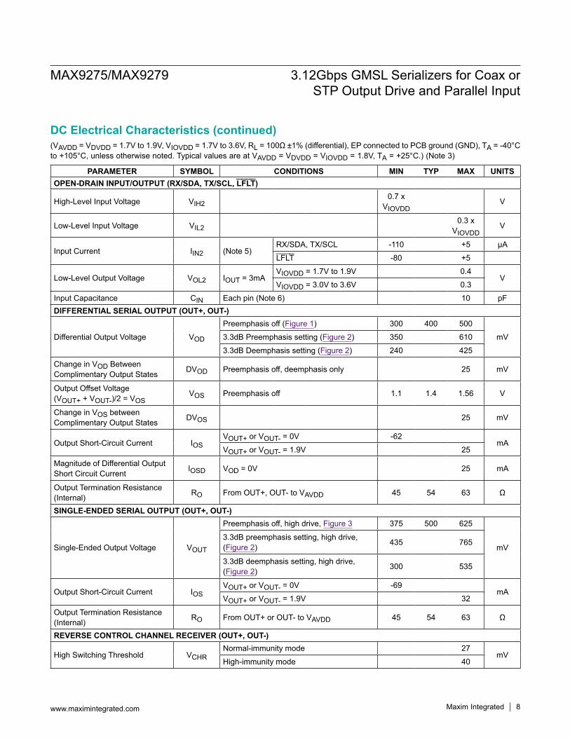
PARAMETER SYMBOL CONDITIONS MIN TYP MAX UNITSOPEN-DRAIN INPUT/OUTPUT (RX/SDA, TX/SCL, LFLT)
High-Level Input Voltage VIH20.7 x
VIOVDDV
Low-Level Input Voltage VIL20.3 x
VIOVDDV
Input Current IIN2 (Note 5)RX/SDA, TX/SCL -110 +5 µALFLT -80 +5
Low-Level Output Voltage VOL2 IOUT = 3mAVIOVDD = 1.7V to 1.9V 0.4
VVIOVDD = 3.0V to 3.6V 0.3
Input Capacitance CIN Each pin (Note 6) 10 pFDIFFERENTIAL SERIAL OUTPUT (OUT+, OUT-)
Differential Output Voltage VOD
Preemphasis off (Figure 1) 300 400 500mV3.3dB Preemphasis setting (Figure 2) 350 610
3.3dB Deemphasis setting (Figure 2) 240 425
Change in VOD Between Complimentary Output States DVOD Preemphasis off, deemphasis only 25 mV
Output Offset Voltage(VOUT+ + VOUT-)/2 = VOS
VOS Preemphasis off 1.1 1.4 1.56 V
Change in VOS between Complimentary Output States DVOS 25 mV
Output Short-Circuit Current IOSVOUT+ or VOUT- = 0V -62
mAVOUT+ or VOUT- = 1.9V 25
Magnitude of Differential Output Short Circuit Current IOSD VOD = 0V 25 mA
Output Termination Resistance (Internal) RO From OUT+, OUT- to VAVDD 45 54 63 Ω
SINGLE-ENDED SERIAL OUTPUT (OUT+, OUT-)
Single-Ended Output Voltage VOUT
Preemphasis off, high drive, Figure 3 375 500 625
mV3.3dB preemphasis setting, high drive, (Figure 2) 435 765
3.3dB deemphasis setting, high drive, (Figure 2) 300 535
Output Short-Circuit Current IOSVOUT+ or VOUT- = 0V -69
mAVOUT+ or VOUT- = 1.9V 32
Output Termination Resistance (Internal) RO From OUT+ or OUT- to VAVDD 45 54 63 Ω
REVERSE CONTROL CHANNEL RECEIVER (OUT+, OUT-)
High Switching Threshold VCHRNormal-immunity mode 27
mVHigh-immunity mode 40
DC Electrical Characteristics (continued)
(VAVDD = VDVDD = 1.7V to 1.9V, VIOVDD = 1.7V to 3.6V, RL = 100Ω ±1% (differential), EP connected to PCB ground (GND), TA = -40°C to +105°C, unless otherwise noted. Typical values are at VAVDD = VDVDD = VIOVDD = 1.8V, TA = +25°C.) (Note 3)
MAX9275/MAX9279 3.12Gbps GMSL Serializers for Coax or STP Output Drive and Parallel Input
www.maximintegrated.com Maxim Integrated 9
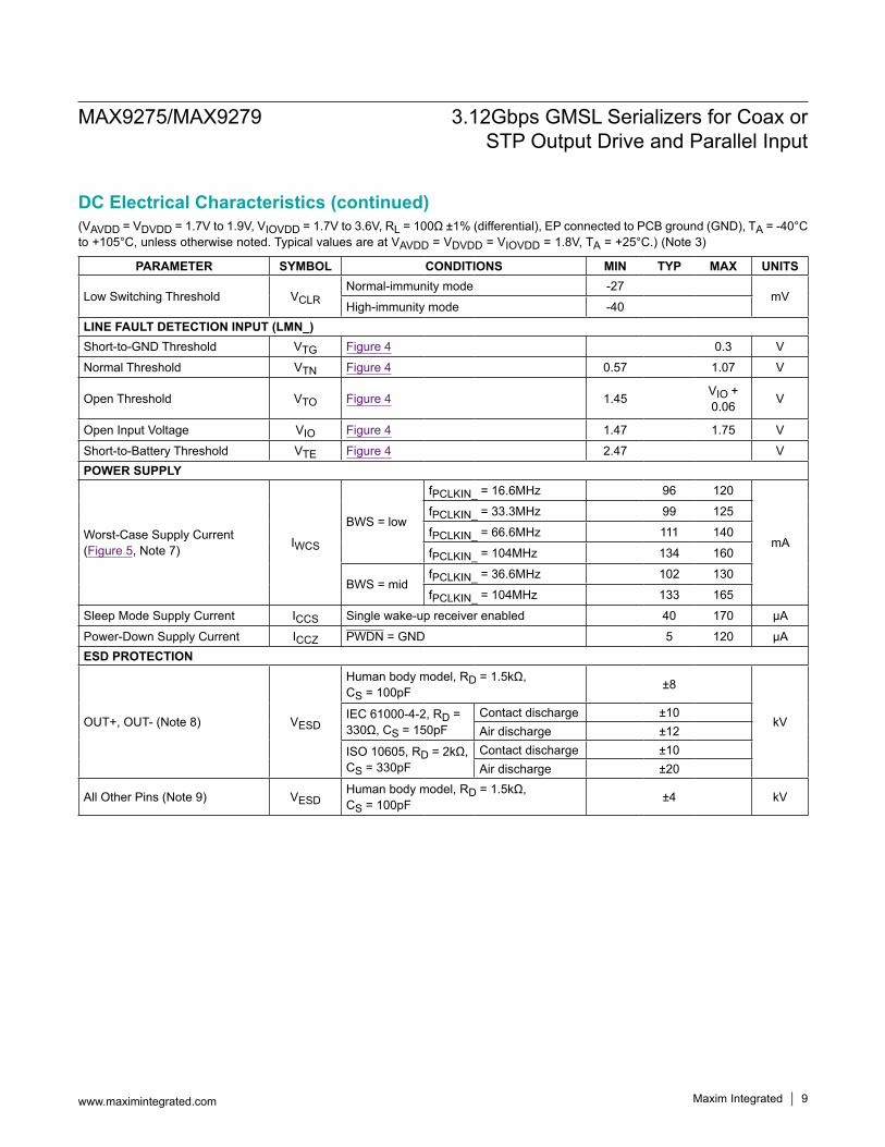
PARAMETER SYMBOL CONDITIONS MIN TYP MAX UNITS
Low Switching Threshold VCLRNormal-immunity mode -27
mVHigh-immunity mode -40
LINE FAULT DETECTION INPUT (LMN_)Short-to-GND Threshold VTG Figure 4 0.3 VNormal Threshold VTN Figure 4 0.57 1.07 V
Open Threshold VTO Figure 4 1.45 VIO + 0.06 V
Open Input Voltage VIO Figure 4 1.47 1.75 VShort-to-Battery Threshold VTE Figure 4 2.47 VPOWER SUPPLY
Worst-Case Supply Current (Figure 5, Note 7) IWCS
BWS = low
fPCLKIN_ = 16.6MHz 96 120
mA
fPCLKIN_ = 33.3MHz 99 125fPCLKIN_ = 66.6MHz 111 140fPCLKIN_ = 104MHz 134 160
BWS = midfPCLKIN_ = 36.6MHz 102 130fPCLKIN_ = 104MHz 133 165
Sleep Mode Supply Current ICCS Single wake-up receiver enabled 40 170 µAPower-Down Supply Current ICCZ PWDN = GND 5 120 µAESD PROTECTION
OUT+, OUT- (Note 8) VESD
Human body model, RD = 1.5kΩ, CS = 100pF ±8
kVIEC 61000-4-2, RD = 330Ω, CS = 150pF
Contact discharge ±10Air discharge ±12
ISO 10605, RD = 2kΩ, CS = 330pF
Contact discharge ±10Air discharge ±20
All Other Pins (Note 9) VESDHuman body model, RD = 1.5kΩ, CS = 100pF ±4 kV
DC Electrical Characteristics (continued)
(VAVDD = VDVDD = 1.7V to 1.9V, VIOVDD = 1.7V to 3.6V, RL = 100Ω ±1% (differential), EP connected to PCB ground (GND), TA = -40°C to +105°C, unless otherwise noted. Typical values are at VAVDD = VDVDD = VIOVDD = 1.8V, TA = +25°C.) (Note 3)
MAX9275/MAX9279 3.12Gbps GMSL Serializers for Coax or STP Output Drive and Parallel Input
www.maximintegrated.com Maxim Integrated 10
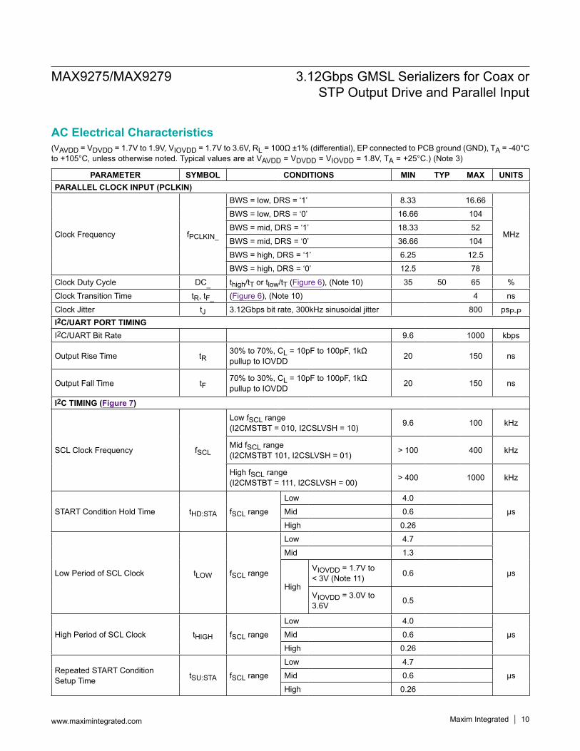
PARAMETER SYMBOL CONDITIONS MIN TYP MAX UNITSPARALLEL CLOCK INPUT (PCLKIN)
Clock Frequency fPCLKIN_
BWS = low, DRS = ‘1’ 8.33 16.66
MHz
BWS = low, DRS = ‘0’ 16.66 104BWS = mid, DRS = ‘1’ 18.33 52BWS = mid, DRS = ‘0’ 36.66 104BWS = high, DRS = ‘1’ 6.25 12.5BWS = high, DRS = ‘0’ 12.5 78
Clock Duty Cycle DC_ thigh/tT or tlow/tT (Figure 6), (Note 10) 35 50 65 %Clock Transition Time tR, tF_ (Figure 6), (Note 10) 4 nsClock Jitter tJ 3.12Gbps bit rate, 300kHz sinusoidal jitter 800 psP-PI2C/UART PORT TIMINGI2C/UART Bit Rate 9.6 1000 kbps
Output Rise Time tR30% to 70%, CL = 10pF to 100pF, 1kΩ pullup to IOVDD 20 150 ns
Output Fall Time tF70% to 30%, CL = 10pF to 100pF, 1kΩ pullup to IOVDD 20 150 ns
I2C TIMING (Figure 7)
SCL Clock Frequency fSCL
Low fSCL range(I2CMSTBT = 010, I2CSLVSH = 10) 9.6 100 kHz
Mid fSCL range (I2CMSTBT 101, I2CSLVSH = 01) > 100 400 kHz
High fSCL range(I2CMSTBT = 111, I2CSLVSH = 00) > 400 1000 kHz
START Condition Hold Time tHD:STA fSCL rangeLow 4.0
µsMid 0.6High 0.26
Low Period of SCL Clock tLOW fSCL range
Low 4.7
µs
Mid 1.3
High
VIOVDD = 1.7V to < 3V (Note 11) 0.6
VIOVDD = 3.0V to 3.6V 0.5
High Period of SCL Clock tHIGH fSCL rangeLow 4.0
µsMid 0.6High 0.26
Repeated START Condition Setup Time tSU:STA fSCL range
Low 4.7µsMid 0.6
High 0.26
AC Electrical Characteristics
(VAVDD = VDVDD = 1.7V to 1.9V, VIOVDD = 1.7V to 3.6V, RL = 100Ω ±1% (differential), EP connected to PCB ground (GND), TA = -40°C to +105°C, unless otherwise noted. Typical values are at VAVDD = VDVDD = VIOVDD = 1.8V, TA = +25°C.) (Note 3)
MAX9275/MAX9279 3.12Gbps GMSL Serializers for Coax or STP Output Drive and Parallel Input
www.maximintegrated.com Maxim Integrated 11
PARAMETER SYMBOL CONDITIONS MIN TYP MAX UNITS
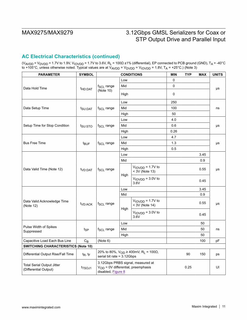
Data Hold Time tHD:DATfSCL range (Note 10)
Low 0
µsMid 0
High 0
Data Setup Time tSU:DAT fSCL rangeLow 250
nsMid 100High 50
Setup Time for Stop Condition tSU:STO fSCL rangeLow 4.0
µsMid 0.6High 0.26
Bus Free Time tBUF fSCL rangeLow 4.7
µsMid 1.3High 0.5
Data Valid Time (Note 12) tVD:DAT fSCL range
Low 3.45
µs
Mid 0.9
High
VIOVDD = 1.7V to < 3V (Note 13) 0.55
VIOVDD = 3.0V to 3.6V 0.45
Data Valid Acknowledge Time (Note 12) tVD:ACK fSCL range
Low 3.45
µs
Mid 0.9
High
VIOVDD = 1.7V to < 3V (Note 14) 0.55
VIOVDD = 3.0V to 3.6V 0.45
Pulse Width of Spikes Suppressed tSP fSCL range
Low 50nsMid 50
High 50Capacitive Load Each Bus Line CB (Note 6) 100 pFSWITCHING CHARACTERISTICS (Note 10)
Differential Output Rise/Fall Time tR, tF20% to 80%, VOD ≥ 400mV, RL = 100Ω, serial bit rate = 3.12Gbps 90 150 ps
Total Serial Output Jitter (Differential Output) tTSOJ1
3.12Gbps PRBS signal, measured at VOD = 0V differential, preemphasis disabled, Figure 8
0.25 UI
AC Electrical Characteristics (continued)
(VAVDD = VDVDD = 1.7V to 1.9V, VIOVDD = 1.7V to 3.6V, RL = 100Ω ±1% (differential), EP connected to PCB ground (GND), TA = -40°C to +105°C, unless otherwise noted. Typical values are at VAVDD = VDVDD = VIOVDD = 1.8V, TA = +25°C.) (Note 3)
Note 3: Limits are 100% production tested at TA = +105°C. Limits over the operating temperature range and are guaranteed by design and characterization, unless otherwise noted.
Note 4: To provide a midlevel, leave the input open, or, if driven, put driver in high impedance. High-impedance leakage current must be less than ±10µA.
Note 5: IIN MIN due to voltage drop across the internal pullup resistor.Note 6: Not production tested. Guaranteed by designNote 7: HDCP not enabled (MAX9279 only). See Table 21 for additional supply current when HDCP is enabled.Note 8: Specified pin to ground.Note 9: Specified pin to all supply/ground.Note 10: Not production tested. Guaranteed by design and characterization. Note 11: The I2C bus standard tLOW min = 0.5µs. Note 12: I2C valid times apply only when the device is operating as a local-side device.Note 13: The I2C bus standard tVD:DAT max = 0.45µs. Note 14: The I2C bus standard tVD:ACK max = 0.45µs.Note 15: Measured in serial link bit times. Bit time = 1/ (30 x fPCLKIN) for BWS = ‘0’ or open. Bit time = 1/ (40 x fPCLKIN) for
BWS = ‘1’.
MAX9275/MAX9279 3.12Gbps GMSL Serializers for Coax or STP Output Drive and Parallel Input
www.maximintegrated.com Maxim Integrated 12
PARAMETER SYMBOL CONDITIONS MIN TYP MAX UNITS
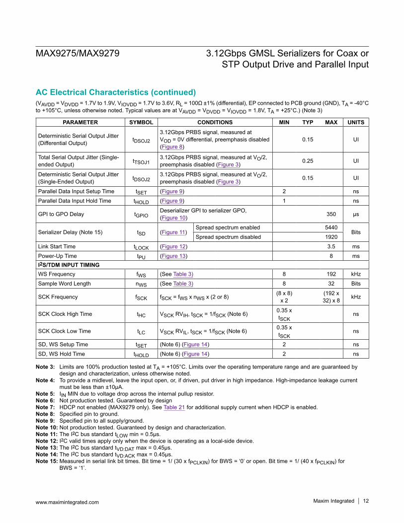
Deterministic Serial Output Jitter (Differential Output) tDSOJ2
3.12Gbps PRBS signal, measured at VOD = 0V differential, preemphasis disabled (Figure 8)
0.15 UI
Total Serial Output Jitter (Single-ended Output) tTSOJ1
3.12Gbps PRBS signal, measured at VO/2, preemphasis disabled (Figure 3) 0.25 UI
Deterministic Serial Output Jitter (Single-Ended Output) tDSOJ2
3.12Gbps PRBS signal, measured at VO/2, preemphasis disabled (Figure 3) 0.15 UI
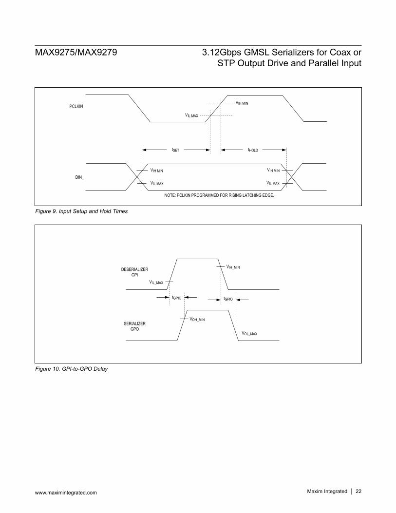
Parallel Data Input Setup Time tSET (Figure 9) 2 nsParallel Data Input Hold Time tHOLD (Figure 9) 1 ns
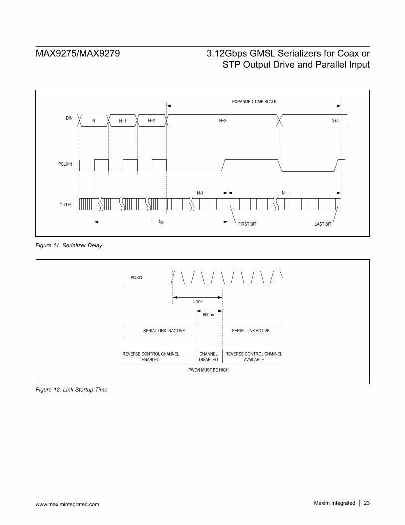
GPI to GPO Delay tGPIODeserializer GPI to serializer GPO, (Figure 10) 350 µs
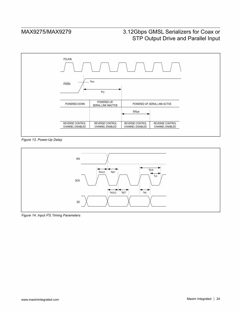
Serializer Delay (Note 15) tSD (Figure 11)Spread spectrum enabled 5440
BitsSpread spectrum disabled 1920
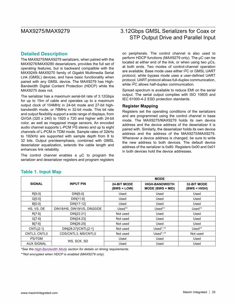
Link Start Time tLOCK (Figure 12) 3.5 msPower-Up Time tPU (Figure 13) 8 msI2S/TDM INPUT TIMINGWS Frequency fWS (See Table 3) 8 192 kHzSample Word Length nWS (See Table 3) 8 32 Bits
SCK Frequency fSCK fSCK = fWS x nWS x (2 or 8) (8 x 8) x 2
(192 x 32) x 8 kHz
SCK Clock High Time tHC VSCK RVIH, tSCK = 1/fSCK (Note 6) 0.35 x tSCK
ns
SCK Clock Low Time tLC VSCK RVIL, tSCK = 1/fSCK (Note 6) 0.35 x tSCK
ns
SD, WS Setup Time tSET (Note 6) (Figure 14) 2 nsSD, WS Hold Time tHOLD (Note 6) (Figure 14) 2 ns
AC Electrical Characteristics (continued)
(VAVDD = VDVDD = VIOVDD = 1.8V, TA = +25°C, unless otherwise noted.)
MAX9275/MAX9279 3.12Gbps GMSL Serializers for Coax or STP Output Drive and Parallel Input
Maxim Integrated 13www.maximintegrated.com
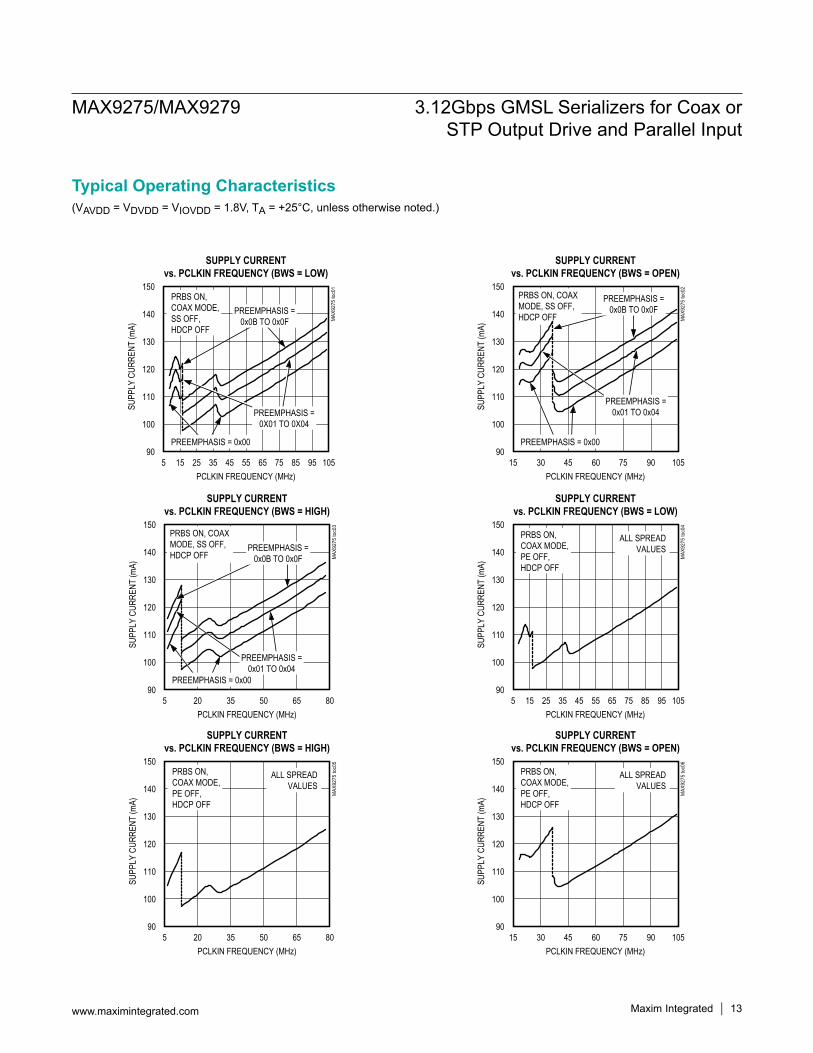
SUPPLY CURRENTvs. PCLKIN FREQUENCY (BWS = LOW)
MAX
9275
toc0
1
PCLKIN FREQUENCY (MHz)
SUPP
LY C
URRE
NT (m
A)
958575655545352515
100
110
120
130
140
150
905 105
PRBS ON,COAX MODE,SS OFF,HDCP OFF
PREEMPHASIS =0x0B TO 0x0F
PREEMPHASIS =0X01 TO 0X04
PREEMPHASIS = 0x00
SUPPLY CURRENTvs. PCLKIN FREQUENCY (BWS = HIGH)
MAX
9275
toc0
3
PCLKIN FREQUENCY (MHz)
SUPP
LY C
URRE
NT (m
A)
65503520
100
110
120
130
140
150
905 80
PRBS ON, COAXMODE, SS OFF,HDCP OFF
PREEMPHASIS = 0x00
PREEMPHASIS =0x01 TO 0x04
PREEMPHASIS =0x0B TO 0x0F
SUPPLY CURRENTvs. PCLKIN FREQUENCY (BWS = HIGH)
MAX
9275
toc0
5
PCLKIN FREQUENCY (MHz)
SUPP
LY C
URRE
NT (m
A)
65503520
100
110
120
130
140
150
905 80
PRBS ON,COAX MODE,PE OFF,HDCP OFF
ALL SPREADVALUES
SUPPLY CURRENTvs. PCLKIN FREQUENCY (BWS = OPEN)
MAX
9275
toc0
2
PCLKIN FREQUENCY (MHz)SU
PPLY
CUR
RENT
(mA)
9075604530
100
110
120
130
140
150
9015 105
PRBS ON, COAXMODE, SS OFF,HDCP OFF
PREEMPHASIS = 0x00
PREEMPHASIS =0x0B TO 0x0F
PREEMPHASIS =0x01 TO 0x04
SUPPLY CURRENTvs. PCLKIN FREQUENCY (BWS = LOW)
MAX
9275
toc0
4
PCLKIN FREQUENCY (MHz)
SUPP
LY C
URRE
NT (m
A)
958575655545352515
100
110
120
130
140
150
905 105
PRBS ON,COAX MODE,PE OFF,HDCP OFF
ALL SPREADVALUES
SUPPLY CURRENTvs. PCLKIN FREQUENCY (BWS = OPEN)
MAX
9275
toc0
6
PCLKIN FREQUENCY (MHz)
SUPP
LY C
URRE
NT (m
A)
9075604530
100
110
120
130
140
150
9015 105
PRBS ON,COAX MODE,PE OFF,HDCP OFF
ALL SPREADVALUES
Typical Operating Characteristics
(VAVDD = VDVDD = VIOVDD = 1.8V, TA = +25°C, unless otherwise noted.)
MAX9275/MAX9279 3.12Gbps GMSL Serializers for Coax or STP Output Drive and Parallel Input
Maxim Integrated 14www.maximintegrated.com
OUTPUT SPECTRUM vs. PCLKINFREQUENCY (VARIOUS SPREAD)
MAX
9275
toc0
7
PCLKIN FREQUENCY (MHz)
OUTP
UT P
OWER
(dBm
)
717068 6964 65 66 6763
-90-80-70-60-50-40-30-20-10
010
-10062
0%SPREAD 0.5%
SPREAD
1% SPREAD2% SPREAD
4% SPREAD
fPCLKIN = 66.6MHz
CABLE LENGTH (m)
PCLK
IN F
REQU
ENCY
(MHz
)
2015105
20
40
60
80
100
120
00 25
MAXIMUM PCLKIN FREQUENCYvs. COAX CABLE LENGTH (BER ≤ 10-10)
MAX
9275
toc0
9
NO PE, 10.7dB EQ
NO PE/EQOPTIMUM PE/EQ
BER CAN BE AS LOW AS 10-12 FORCABLE LENGTHS LESS THAN 15m
OUTPUT SPECTRUM vs. PCLKINFREQUENCY (VARIOUS SPREAD)
MAX
9275
toc0
8
PCLKIN FREQUENCY (MHz)OU
TPUT
POW
ER (d
Bm)
35.535.034.0 34.532.0 32.5 33.0 33.531.5
-80
-70
-60
-50
-40
-30
-20
-10
0
10
-9031.0
fPCLKIN = 33.3MHz0%
SPREAD 0.5%SPREAD
1% SPREAD
2% SPREAD
4% SPREAD
Typical Operating Characteristics (continued)
MAX9275/MAX9279 3.12Gbps GMSL Serializers for Coax or STP Output Drive and Parallel Input
www.maximintegrated.com Maxim Integrated 15
TOP VIEW
MAX9275MAX9279
TQFN(8mm x 8mm x 0.75mm)
25
26
15
16
17
18
19
20
21
22
23
24
CONF3
+
IOVDD
27
28
MS/CNTL0
CDS/CNTL3
DIN23
DVDD
DIN24
DIN25
DIN26
DIN27/CNTL1
DIN28/CNTL2
SD
SCK
WS
54
53
52
51
50
49
48
47
46
45
44
43
1 2 3 4 5 6 7 8 9 10 11 12 13 14
DVDD
DIN9
56
55
DIN11
*CONNECT EP TO GROUND PLANE
DIN10EP*
DIN8
DIN7
DIN6
DIN5
DIN4
DIN3
DIN2
DIN1
IOVDD
DIN0
DIN2
0/DE
DIN1
9/VS
DIN2
2
DIN2
1
DIN1
8/HS
DIN1
7
AVDD
IOVD
D
PCLK
IN
DIN1
6
DIN1
5
DIN1
4
DIN1
3
DIN1
236 35 34 33 32 31 30 2940 39 38 37
LMN0
LFLT
GPO
/HIM
CONF
0
42 41
CONF
2
BWS
PWDN
RX/S
DA
TX/S
CL
CONF
1
LMN1
OUT-
OUT+
AVDD
PIN NAME FUNCTION1–5, 9, 43,
45–53, 55, 56 DIN[17:0] Parallel Data Inputs with Internal Pulldown to EP. Encrypted when HDCP is enabled (MAX9279 only).
6 PCLKIN Parallel Clock Input with Internal Pulldown to EP. Latches parallel data inputs and provides the PLL reference clock.
7, 26, 44 IOVDDI/O Supply Voltage. 1.8V to 3.3V logic I/O power supply. Bypass IOVDD to EP with 0.1µF and 0.001µF capacitors as close as possible to the device with the smallest value capacitor closest to IOVDD.
8, 36 AVDD 1.8V Analog Power Supply. Bypass AVDD to EP with 0.1µF and 0.001µF capacitors as close as possible to the device with the smaller capacitor closest to AVDD.
10 DIN18/HS
Parallel Data Input/Horizontal Sync with Internal Pulldown to EP. Defaults to parallel data input on power-up.Horizontal sync input when HDCP is enabled (MAX9279 only) or when in high-bandwidth mode (BWS = open).
Pin Configuration
Pin Description
MAX9275/MAX9279 3.12Gbps GMSL Serializers for Coax or STP Output Drive and Parallel Input
www.maximintegrated.com Maxim Integrated 16
PIN NAME FUNCTION
11 DIN19/VS
Parallel Data Input/Vertical Sync with Internal Pulldown to EP. Defaults to parallel data input on power-up.Vertical sync input when HDCP is enabled (MAX9279 only) or when in high-bandwidth mode (BWS = open).
12 DIN20/DE
Parallel Data Input/Device Enable with Internal Pulldown to EP. Defaults to parallel data input on power-up.Device enable input when HDCP is enabled (MAX9279 only) or when in high-bandwidth mode (BWS = open).
13–15, 17–19 DIN[26:21] Parallel Data Inputs with Internal Pulldown to EP. Encrypted when HDCP is enabled (MAX9279 only). DIN[26:21] used only in 32-bit and high-bandwidth modes (BWS = high or open).
16, 54 DVDD 1.8V Digital Power Supply. Bypass DVDD to EP with 0.1µF and 0.001µF capacitors as close as possible to the device with the smaller value capacitor closest to DVDD.
20 DIN27/CNTL1
Parallel Data/Auxiliary Control Signal Input with Internal Pulldown to EP.DIN27 used only in 32-bit mode (BWS = high). DIN27 not encrypted when HDCP is enabled (MAX9279 only).CNTL1 used only in high-bandwidth mode (BWS = open). CNTL1 not encrypted when HDCP is enabled (MAX9279 only).
21 DIN28/CNTL2
Parallel Data/Auxiliary Control Signal Input with Internal Pulldown to EP.DIN28 used only in 32-bit mode (BWS = high). DIN28 not encrypted when HDCP is enabled (MAX9279 only).CNTL2 used only in high-bandwidth mode (BWS = open). CNTL2 not encrypted when HDCP is enabled (MAX9279 only).
22 SDI2S/TDM Serial-Data Input with Internal Pulldown to EP. Disable I2S/TDM encoding to use SD as an additional control/data input latched on the selected edge of PCLKIN. Encrypted when HDCP is enabled.
23 SCK I2S/TDM Serial-Clock Input with Internal Pulldown to EP24 WS I2S/TDM Word-Select Input with Internal Pulldown to EP
25 CONF3 Three-Level Configuration Input. See Table 11 for details. Use 6kΩ (max) for pullup to IOVDD/pulldown to GND.
27 MS/CNTL0
Mode Select/Auxiliary Control Signal Input with Internal Pulldown to EP. Function is determined by the MSCNTL0 register bit and defaults to MS on power-up.MS (MSCNTL0 = 0): Set MS = low, to select base mode. Set MS = high to select the bypass mode.CNTL0 (MSCNTL0 = 1): Used only in high-bandwidth mode (BWS = open). CNTL0 not encrypted when HDCP is enabled (MAX9279 only).
28 CDS/CNTL3
Control Direction Selection/Auxiliary Control Signal Input with Internal Pulldown to EP. Function is determined by the CDSCNTL3 register bit and defaults to CDS on power-up.CDS (CDSCNTL3 = 0): Control link direct selection input with internal pulldown to EP. Set CDS = low when the control channel master µC is connected at the serializer. Set CDS = high when the control channel master µC is connected at the deserializer.CNTL3 (CDSCNTL3 = 1): Used only in high-bandwidth mode (BWS = open). CNTL3 not encrypted when HDCP is enabled (MAX9279 only).
Pin Description (continued)
MAX9275/MAX9279 3.12Gbps GMSL Serializers for Coax or STP Output Drive and Parallel Input
www.maximintegrated.com Maxim Integrated 17
PIN NAME FUNCTION
29 PWDN Active-Low, Power-Down Input with Internal Pulldown to EP. Set PWDN low to enter power-down mode to reduce power consumption.
30 RX/SDA
UART Receive/I2C Serial Data Input/Output with Internal 30kΩ Pullup to IOVDD. Function is determined by the state of CONF[1:0] at power-up (Table 10). RX/SDA has an open-drain driver and requires a pullup resistor.RX: Input of the serializer’s UART.SDA: Data input/output of the serializer’s I2C master/slave.
31 TX/SCL
UART Transmit/I2C Serial Clock Input/Output with Internal 30kΩ Pullup to IOVDD. Function is determined by the state of CONF[1:0] at power-up (Table 10). TX/SCL has an open-drain driver and requires a pullup resistor.TX: Output of the serializer’s UART.SCL: Clock input/output of the serializer’s I2C master/slave.
32 CONF1 Three-Level Configuration Input. See Table 10 for details. Use 6kΩ (max) for pullup to IOVDD/pulldown to GND.
33 LMN1 Line-Fault Monitor Input 1 (see Figure 4)34 OUT- Inverting CML Coax/Twisted-Pair Serial Output35 OUT+ Noninverting CML Coax/Twisted-Pair Serial Output37 LMN0 Line-Fault Monitor Input 0 (see Figure 4)
38 LFLT Active-Low Open-Drain Line-Fault Output. LFLT has a 60kΩ internal pullup to IOVDD. LFLT = low indicates a line fault. LFLT is output high when PWDN = low.
39 GPO/HIM
General-Purpose Output/High-Immunity Mode Input.Functions as HIM input with internal pulldown to EP at power-up or when resuming from power-down mode (PWDN = low), and switches to GPO output automatically after power-up.HIM: Default HIGHIMM bit value is latched at power-up or when resuming from power-down mode (PWDN = low) and is active high. Connect HIM to IOVDD with a 30kΩ or less pullup resistor to set high or leave open to set low. HIGHIMM can be programmed to a different value after power-up. HIGHIMM in the deserializer must be set to the same value.GPO: Output follows the state of the GPI (or INT) input on the deserializer. GPO is low after power-up or when PWDN is low.
40 CONF0Three-Level Configuration Input. The state of CONF0 latches at power-up or when resuming from power-down mode (PWDN = low). See Table 10 for details. Use 6kΩ (max) for pullup to IOVDD/pulldown to GND.
41 CONF2Three-Level Configuration Input. The state of CONF2 latches at power-up or when resuming from power-down mode (PWDN = low). See Table 11 for details. Use 6kΩ (max) for pullup to IOVDD/pulldown to GND.
42 BWSThree-Level Bus Width Select Input. Set BWS to the same level on both sides of the serial link. Set BWS = low with 6kΩ (max) pulldown for 24 bit mode. Set BWS = 6kΩ (max) pullup to IOVDD high for 32-bit mode. Set BWS = open for high-bandwidth mode.
— EP Exposed Pad. EP is internally connected to device ground. must connect EP to the PCB ground plane through an array of vias for proper thermal and electrical performance.
Pin Description (continued)
MAX9275/MAX9279 3.12Gbps GMSL Serializers for Coax or STP Output Drive and Parallel Input
www.maximintegrated.com Maxim Integrated 18
SCRAMBLE/PARITY/8b/10b/9b/10b/
ENCODE
PARALLELTO
SERIAL
MAX9275MAX9279
REVERSECONTROLCHANNEL
HDCPENCRYPT
(MAX9279ONLY)
HDCPDECRYPT
CONTROLMS, CDS
UART/I2C
GPO/HIMSD SCK WS TX /SCL RX/SDA BWS CONF[3:0]
HDCPKEYS
RGB
HSVSDE
HSVSDE
ACB
CNTL[3:0](9b10b)
DIN[28:27](30-BIT)
FCC
HDCPCONTROL
I2S/TDMMS, CDS
FIFO
CONTROL(9b10b)
SYNC
VIDEO
CLKDIV
SSPLL
CNTL0, CNTL3(9b10b)
CNTL[2:1](9b10b)
DOUT[28:27](30-BIT)
MS/CNTL0CDS/CNTL3
DIN27/CNTL1DIN28/CNTL2
DIN19/VSDIN18/HS
DIN[26:21]
DIN[17:0]
PCLKIN
DIN20/DE
RGB[23:18](30-BIT OR 9b10b)
RGB[17:0]
CML TX
LMN1
LMN0
LFLT
OUT+
OUT-
RX
PWDN
FILTERPLL LINE
FAULTDETECT
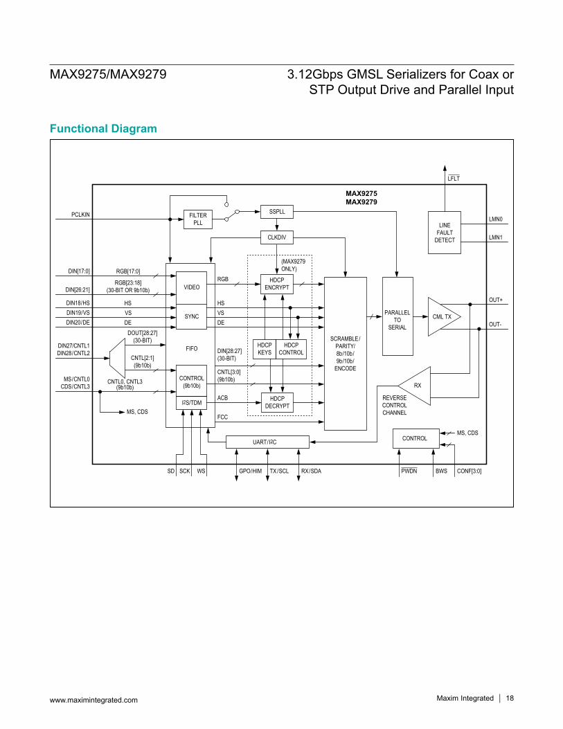
Functional Diagram
MAX9275/MAX9279 3.12Gbps GMSL Serializers for Coax or STP Output Drive and Parallel Input
www.maximintegrated.com Maxim Integrated 19
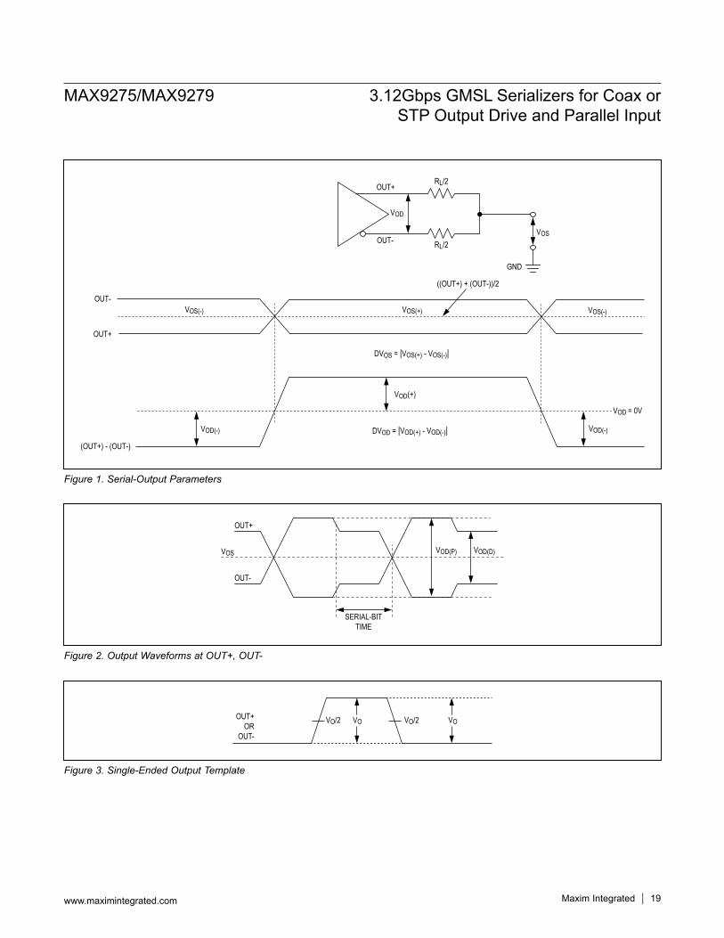
Figure 1. Serial-Output Parameters
Figure 2. Output Waveforms at OUT+, OUT-
Figure 3. Single-Ended Output Template
OUT-
VOD
VOS
GND
RL/2
RL/2
OUT+
OUT-
OUT+
(OUT+) - (OUT-)
VOS(-) VOS(+)
((OUT+) + (OUT-))/2
VOS(-)
VOD(-)VOD(-)
VOD = 0V
DVOS = |VOS(+) - VOS(-)|
DVOD = |VOD(+) - VOD(-)|
VOD(+)
OUT+
OUT-
VOS VOD(P) VOD(D)
SERIAL-BITTIME
OUT+OR
OUT-
VO/2 VO/2VO VO
MAX9275/MAX9279 3.12Gbps GMSL Serializers for Coax or STP Output Drive and Parallel Input
www.maximintegrated.com Maxim Integrated 20
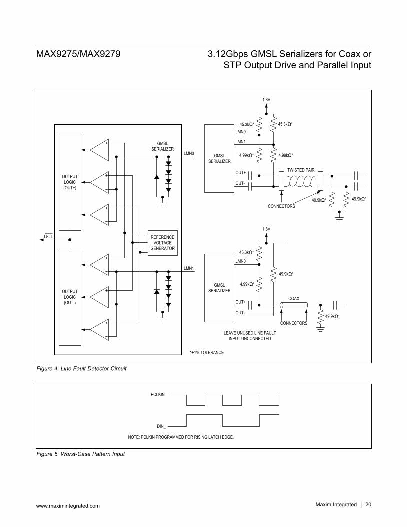
Figure 4. Line Fault Detector Circuit
Figure 5. Worst-Case Pattern Input
OUTPUTLOGIC(OUT+)
LFLT REFERENCEVOLTAGE
GENERATOR
CONNECTORS
*±1% TOLERANCE
LEAVE UNUSED LINE FAULTINPUT UNCONNECTED
OUTPUTLOGIC(OUT-)
GMSLSERIALIZER
GMSLSERIALIZER
45.3kΩ*
45.3kΩ*
49.9kΩ*
49.9kΩ*
4.99kΩ*
49.9kΩ*
4.99kΩ*
4.99kΩ*
49.9kΩ*
45.3kΩ*
LMN1
LMN1
LMN0
LMN0
1.8V
TWISTED PAIR
COAX
OUT+
OUT-
CONNECTORS
GMSLSERIALIZER
LMN0
1.8V
OUT+
OUT-
PCLKIN
NOTE: PCLKIN PROGRAMMED FOR RISING LATCH EDGE.
DIN_
MAX9275/MAX9279 3.12Gbps GMSL Serializers for Coax or STP Output Drive and Parallel Input
www.maximintegrated.com Maxim Integrated 21
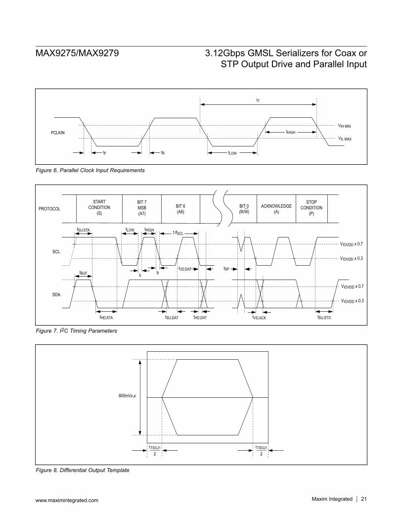
Figure 6. Parallel Clock Input Requirements
Figure 7. I2C Timing Parameters
Figure 8. Differential Output Template
VIL MAX
tHIGH
tLOW
tT
tRtF
VIH MINPCLKIN
PROTOCOL
SCL
SDA
STARTCONDITION
(S)
BIT 7MSB(A7)
BIT 6(A6)
BIT 0(R/W)
ACKNOWLEDGE(A)
STOPCONDITION
(P)
VIOVDD x 0.7
VIOVDD x 0.3
VIOVDD x 0.7
VIOVDD x 0.3
tSU;STA tLOW tHIGH
tBUF
tHD;STA
trtSPtVD;DAT
tf
tSU;DAT tHD;DAT tSU;STO
1/fSCL
tVD;ACK
800mVP-P
tTSOJ12
tTSOJ12
MAX9275/MAX9279 3.12Gbps GMSL Serializers for Coax or STP Output Drive and Parallel Input
www.maximintegrated.com Maxim Integrated 22
Figure 9. Input Setup and Hold Times
Figure 10. GPI-to-GPO Delay
VIH MIN
VIH MINVIH MIN
VIL MAX VIL MAX
VIL MAX
PCLKIN
DIN_
tHOLDtSET
NOTE: PCLKIN PROGRAMMED FOR RISING LATCHING EDGE.
tGPIO tGPIO
VOH_MIN
VOL_MAX
VIH_MIN
VIL_MAX
DESERIALIZERGPI
SERIALIZERGPO
MAX9275/MAX9279 3.12Gbps GMSL Serializers for Coax or STP Output Drive and Parallel Input
www.maximintegrated.com Maxim Integrated 23
Figure 11. Serializer Delay
Figure 12. Link Startup Time
tSD FIRST BIT LAST BIT
N
N+3
EXPANDED TIME SCALE
N+4N N+1 N+2
N-1
DIN_
PCLKIN
OUT+/-
SERIAL LINK INACTIVE SERIAL LINK ACTIVE
CHANNELDISABLED
REVERSE CONTROL CHANNELENABLED
tLOCK
500µs
PCLKIN
REVERSE CONTROL CHANNELAVAILABLE
PWDN MUST BE HIGH
MAX9275/MAX9279 3.12Gbps GMSL Serializers for Coax or STP Output Drive and Parallel Input
www.maximintegrated.com Maxim Integrated 24
Figure 13. Power-Up Delay
Figure 14. Input I2S Timing Parameters
PWDN
POWERED DOWN
VIH1
tPU
REVERSE CONTROLCHANNEL DISABLED
500µs
PCLKIN
POWERED UP,SERIAL LINK INACTIVE POWERED UP, SERIAL LINK ACTIVE
REVERSE CONTROLCHANNEL ENABLED
REVERSE CONTROLCHANNEL ENABLED
REVERSE CONTROLCHANNEL DISABLED
WS
tHOLD tSET
tHOLD tSET tHC
tSCK
tLC
SCK
SD
*See the High-Bandwidth Mode section for details on timing requirements.**Not encrypted when HDCP is enabled (MAX9279 only).
MAX9275/MAX9279 3.12Gbps GMSL Serializers for Coax or STP Output Drive and Parallel Input
www.maximintegrated.com Maxim Integrated 25
Detailed DescriptionThe MAX9275/MAX9279 serializers, when paired with the MAX9276/MAX9280 deserializers, provides the full set of operating features, but is backward compatible with the MAX9249–MAX9270 family of Gigabit Multimedia Serial Link (GMSL) devices, and have basic functionality when paired with any GMSL device. The MAX9279 has High-Bandwidth Digital Content Protection (HDCP) while the MAX9275 does not.The serializer has a maximum serial-bit rate of 3.12Gbps for up to 15m of cable and operates up to a maximum output clock of 104MHz in 24-bit mode and 27-bit high-bandwidth mode, or 78MHz in 32-bit mode. This bit rate and output flexibility support a wide range of displays, from QVGA (320 x 240) to 1920 x 720 and higher with 24-bit color, as well as megapixel image sensors. An encoded audio channel supports L-PCM I2S stereo and up to eight channels of L-PCM in TDM mode. Sample rates of 32kHz to 192kHz are supported with sample depth from 8 to 32 bits. Output pre/deemphasis, combined with GMSL deserializer equalization, extends the cable length and enhances link reliability.The control channel enables a µC to program the serializer and deserializer registers and program registers
on peripherals. The control channel is also used to perform HDCP functions (MAX9279 only). The µC can be located at either end of the link, or when using two µCs, at both ends. Two modes of control-channel operation are available. Base mode uses either I2C or GMSL UART protocol, while bypass mode uses a user-defined UART protocol. UART protocol allows full-duplex communication, while I2C allows half-duplex communication.Spread spectrum is available to reduce EMI on the serial output. The serial output complies with ISO 10605 and IEC 61000-4-2 ESD protection standards.
Register MappingRegisters set the operating conditions of the serializers and are programmed using the control channel in base mode. The MAX9275/MAX9279 holds its own device address and the device address of the deserializer it is paired with. Similarly, the deserializer holds its own device address and the address of the MAX9275/MAX9279. Whenever a device address is changed, be sure to write the new address to both devices. The default device address of the serializer is 0x80. Registers 0x00 and 0x01 in both devices hold the device addresses.
Table 1. Input Map
SIGNAL INPUT PINMODE
24-BIT MODE (BWS = LOW)
HIGH-BANDWIDTH MODE (BWS = MID)
32-BIT MODE (BWS = HIGH)
R[5:0] DIN[5:0] Used Used UsedG[5:0] DIN[11:6] Used Used UsedB[5:0] DIN[17:12] Used Used Used
HS, VS, DE DIN18/HS, DIN19/VS, DIN20/DE Used** Used** Used**R[7:6] DIN[22:21] Not used Used UsedG[7:6] DIN[24:23] Not used Used UsedB[7:6] DIN[26:25] Not used Used Used
CNTL[2:1] DIN[28:27]/CNTL[2:1] Not used Used*,** Used**CNTL3, CNTL0 CDS/CNTL3, MS/CNTL0 Not used Used*,** Not used
I2S/TDMWS, SCK, SD
Used Used UsedAUX SIGNAL Used Used Used
MAX9275/MAX9279 3.12Gbps GMSL Serializers for Coax or STP Output Drive and Parallel Input
www.maximintegrated.com Maxim Integrated 26
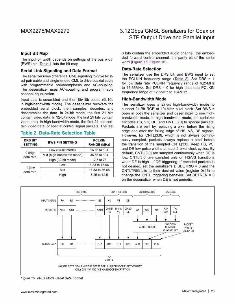
Input Bit MapThe input bit width depends on settings of the bus width (BWS) pin. Table 1 lists the bit map.
Serial Link Signaling and Data FormatThe serializer uses differential CML signaling to drive twist-ed-pair cable and single-ended CML to drive coaxial cable with programmable pre/deemphasis and AC-coupling. The deserializer uses AC-coupling and programmable channel equalization.Input data is scrambled and then 8b/10b coded (9b10b in high-bandwidth mode). The deserializer recovers the embedded serial clock, then samples, decodes, and descrambles the data. In 24-bit mode, the first 21 bits contain video data. In 32-bit mode, the first 29 bits contain video data. In high-bandwidth mode, the first 24 bits con-tain video data, or special control signal packets. The last
3 bits contain the embedded audio channel, the embed-ded forward control channel, the parity bit of the serial word (Figure 15, Figure 16).
Data-Rate SelectionThe serializer use the DRS bit, and BWS input to set the PCLKIN frequency range (Table 2). Set DRS = 1 for low data rate PCLKIN frequency range of 6.25MHz to 16.66MHz. Set DRS = 0 for high data rate PCLKIN frequency range of 12.5MHz to 104MHz.
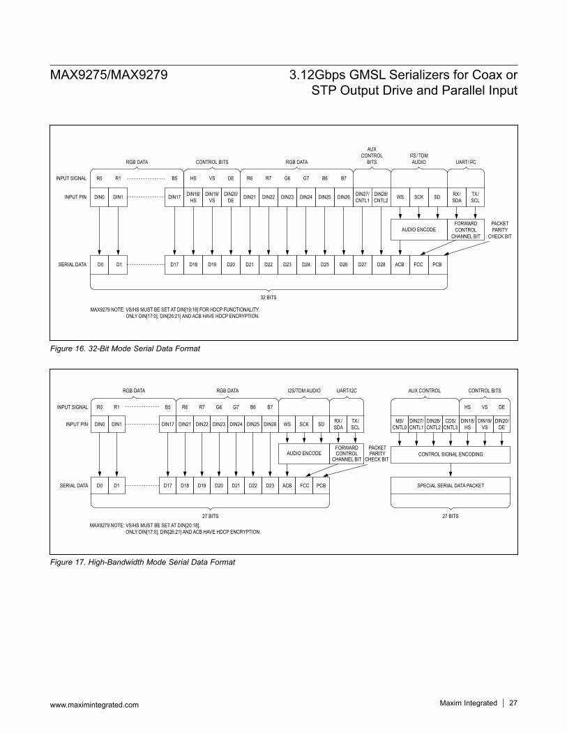
High-Bandwidth ModeThe serializer uses a 27-bit high-bandwidth mode to support 24-Bit RGB at 104MHz pixel clock. Set BWS = open in both the serializer and deserializer to use high-bandwidth mode. In high-bandwidth mode, the serializer encodes HS, VS, DE, and CNTL[3:0] to special packets. Packets are sent by replacing a pixel before the rising edge and after the falling edge of HS, VS, DE signals. However, for CNTL[3:0], which is not always continu-ously sampled, packets always replace a pixel before the transition of the sampled CNTL[3:0]. Keep HS, VS, and DE low pulse widths at least 2 pixel clock cycles. By default, CNTL[3:0] are sampled continuously when DE is low. CNTL[3:0] are sampled only on HS/VS transitions when DE is high . If DE triggering of encoded packets is not desired, set the serializer’s DISDETRIG = 0 and the CNTLTRIG bits to their desired value (register 0x15) to change the CNTL triggering behavior. Set DETREN = 0 on the deserializer when DE is not periodic.
Table 2. Data-Rate Selection Table
Figure 15. 24-Bit Mode Serial Data Format
24 BITS
PACKETPARITY
CHECK BIT
ACB FCC PCBD0 D1
R0 R1 B5 HS VS DE
D20D19D18D17
MAX9279 NOTE: VS/HS MUST BE SET AT DIN[19:18] FOR HDCP FUNCTIONALITY. ONLY DIN[17:0] AND ACB HAVE HDCP ENCRYPTION.
RGB DATA CONTROL BITS
DIN0 DIN1 DIN17 DIN18/HS
DIN19/VS
DIN20/DE
SERIAL DATA
INPUT PIN
INPUT SIGNAL
WS SCK SD RX/SDA
TX/SCL
AUDIO ENCODE
I2S/TDM AUDIO UART/I2C
FORWARDCONTROL
CHANNEL BIT
DRS BIT SETTING BWS PIN SETTING PCLKIN
RANGE (MHz)
0 (high data rate)
Low (24-bit mode) 16.66 to 104Mid (high-bandwidth mode) 36.66 to 104
High (32-bit mode) 12.5 to 78
1 (low data rate)
Low 8.33 to 16.66Mid 18.33 to 36.66High 6.25 to 12.5
MAX9275/MAX9279 3.12Gbps GMSL Serializers for Coax or STP Output Drive and Parallel Input
www.maximintegrated.com Maxim Integrated 27
Figure 16. 32-Bit Mode Serial Data Format
Figure 17. High-Bandwidth Mode Serial Data Format
D23
32 BITS
PACKETPARITY
CHECK BIT
D24 D25 D26 D27 D28 ACB FCC PCB
R6 R7
D0 D1
R0 R1 B5 HS VS DE
D22D21D20D19D18
G6 G7 B6 B7
D17
RGB DATA CONTROL BITS RGB DATA
AUXCONTROL
BITS
DIN0 DIN1 DIN17 DIN18/HS
DIN19/VS
DIN20/DE DIN21 DIN22 DIN23 DIN24 DIN25 DIN26 DIN27/
CNTL1DIN28/CNTL2
SERIAL DATA
INPUT PIN
INPUT SIGNAL
WS SCK SD RX/SDA
TX/SCL
AUDIO ENCODE
I2S/ TDMAUDIO UART/ I2C
FORWARDCONTROL
CHANNEL BIT
MAX9279 NOTE: VS/HS MUST BE SET AT DIN[19:18] FOR HDCP FUNCTIONALITY. ONLY DIN[17:0], DIN[26:21] AND ACB HAVE HDCP ENCRYPTION.
D23
27 BITS
PACKETPARITY
CHECK BIT
ACB FCC PCB
R6 R7
D0 D1
R0 R1 B5 HS VS DE
D22D21D20D19D18
G6 G7 B6 B7
D17
RGB DATA CONTROL BITSRGB DATA AUX CONTROL
DIN0 DIN1 DIN17 DIN18/HS
DIN19/VS
DIN20/DEDIN21 DIN22 DIN23 DIN24 DIN25 DIN26 DIN27/
CNTL1DIN28/CNTL2
SERIAL DATA
INPUT PIN
INPUT SIGNAL
WS SCK SD RX/SDA
TX/SCL
AUDIO ENCODE
I2S/TDM AUDIO UART/I2C
FORWARDCONTROL
CHANNEL BITCONTROL SIGNAL ENCODING
CDS/CNTL3
MS/CNTL0
27 BITS
SPECIAL SERIAL DATA PACKET
MAX9279 NOTE: VS/HS MUST BE SET AT DIN[20:18]. ONLY DIN[17:0], DIN[26:21] AND ACB HAVE HDCP ENCRYPTION.
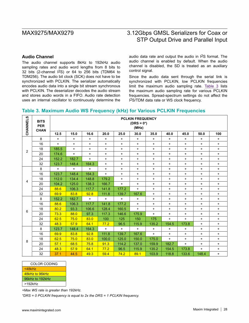
+Max WS rate is greater than 192kHz.*DRS = 0 PCLKIN frequency is equal to 2x the DRS = 1 PCLKIN frequency.
MAX9275/MAX9279 3.12Gbps GMSL Serializers for Coax or STP Output Drive and Parallel Input
www.maximintegrated.com Maxim Integrated 28
Audio ChannelThe audio channel supports 8kHz to 192kHz audio sampling rates and audio word lengths from 8 bits to 32 bits (2-channel I2S) or 64 to 256 bits (TDM64 to TDM256). The audio bit clock (SCK) does not have to be synchronized with PCLKIN. The serializer automatically encodes audio data into a single bit stream synchronous with PCLKIN. The deserializer decodes the audio stream and stores audio words in a FIFO. Audio rate detection uses an internal oscillator to continuously determine the
audio data rate and output the audio in I2S format. The audio channel is enabled by default. When the audio channel is disabled, the SD is treated as an auxiliary control signal.Since the audio data sent through the serial link is synchronized with PCLKIN, low PCLKIN frequencies limit the maximum audio sampling rate. Table 3 lists the maximum audio sampling rate for various PCLKIN frequencies. Spread-spectrum settings do not affect the I2S/TDM data rate or WS clock frequency.
Table 3. Maximum Audio WS Frequency (kHz) for Various PCLKIN Frequencies
CH
AN
NEL
S
BITS PER
CHAN
PCLKIN FREQUENCY(DRS = 0*)
(MHz)12.5 15.0 16.6 20.0 25.0 30.0 35.0 40.0 45.0 50.0 100
2
8 + + + + + + + + + + +16 + + + + + + + + + + +18 185.5 + + + + + + + + + +20 174.6 + + + + + + + + + +24 152.2 182.7 + + + + + + + + +32 123.7 148.4 164.3 + + + + + + + +
4
8 + + + + + + + + + + +16 123.7 148.4 164.3 + + + + + + + +18 112.0 134.4 148.8 179.2 + + + + + + +20 104.2 125.0 138.3 166.7 + + + + + + +24 88.6 106.3 117.7 141.8 177.2 + + + + + +32 69.9 83.8 92.8 111.8 139.7 167.6 + + + + +
6
8 152.2 182.7 + + + + + + + + +16 88.6 106.3 117.7 141.8 177.2 + + + + + +18 80.2 93.3 106.6 128.4 160.5 + + + + + +20 73.3 88.0 97.3 117.3 146.6 175.9 + + + + +24 62.5 75.0 83.0 100 125 150 175 + + + +32 48.3 57.9 64.1 77.2 96.5 115.9 135.2 154.5 173.8 + +
8
8 123.7 148.4 164.3 + + + + + + + +16 69.9 83.8 92.8 111.8 139.7 167.6 + + + + +18 62.5 75.0 83.0 100.0 125.0 150.0 175.0 + + + +20 57.1 68.5 75.8 91.3 114.2 137.0 159.9 182.7 + + +24 48.3 57.9 64.1 77.2 96.5 115.9 135.2 154.5 173.8 + +32 37.1 44.5 49.3 59.4 74.2 89.1 103.9 118.8 133.6 148.4 +
COLOR CODING<48kHz48kHz to 96kHz96kHz to 192kHz>192kHz
MAX9275/MAX9279 3.12Gbps GMSL Serializers for Coax or STP Output Drive and Parallel Input
www.maximintegrated.com Maxim Integrated 29
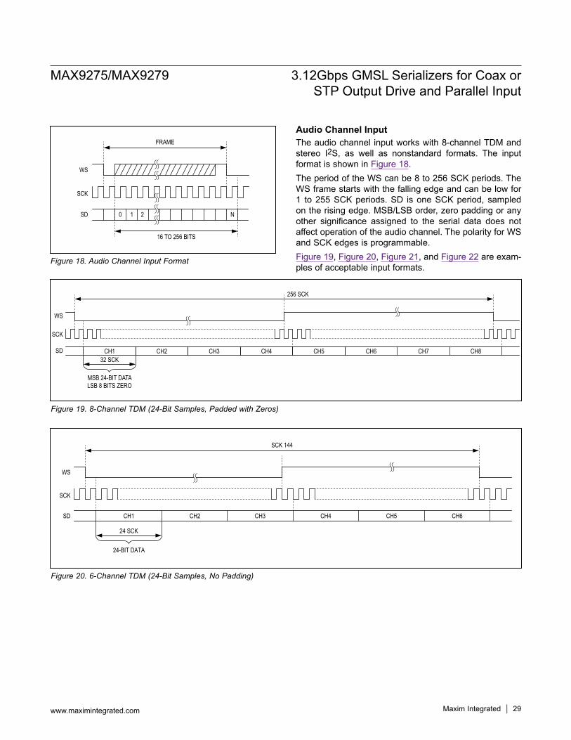
Audio Channel InputThe audio channel input works with 8-channel TDM and stereo I2S, as well as nonstandard formats. The input format is shown in Figure 18.The period of the WS can be 8 to 256 SCK periods. The WS frame starts with the falling edge and can be low for 1 to 255 SCK periods. SD is one SCK period, sampled on the rising edge. MSB/LSB order, zero padding or any other significance assigned to the serial data does not affect operation of the audio channel. The polarity for WS and SCK edges is programmable.Figure 19, Figure 20, Figure 21, and Figure 22 are exam-ples of acceptable input formats.
Figure 18. Audio Channel Input Format
Figure 19. 8-Channel TDM (24-Bit Samples, Padded with Zeros)
Figure 20. 6-Channel TDM (24-Bit Samples, No Padding)
WS
SCK
SD
FRAME
0 1 2 N
16 TO 256 BITS
WS
SCK
SD
256 SCK
CH1 CH2 CH3 CH4 CH5 CH6 CH7 CH8
MSB 24-BIT DATALSB 8 BITS ZERO
32 SCK
WS
SCK
SD
SCK 144
24-BIT DATA
CH1 CH2 CH3 CH4 CH5 CH6
24 SCK
MAX9275/MAX9279 3.12Gbps GMSL Serializers for Coax or STP Output Drive and Parallel Input
www.maximintegrated.com Maxim Integrated 30
Reverse Control ChannelThe serializer uses the reverse control channel to receive I2C/UART, MS, and GPO signals from the deserializer in the opposite direction of the video stream. The reverse control channel and forward video data coexist on the same serial cable forming a bidirectional link. The reverse control channel operates independently from the forward control channel. The reverse control channel is available 2ms after power-up. The serializer temporarily disables the reverse control channel for 500µs after starting/stopping the forward serial link.
Control Channel and Register ProgrammingThe control channel is available for the µC to send and receive control data over the serial link simultaneously with the high-speed data. The µC controls the link from either the serializer or the deserializer side to support video-display or image-sensing applications. The control channel between the µC and serializer or deserializer runs in base mode or bypass mode according to the
mode selection (MS) input of the device connected to the µC. Base mode is a half-duplex control channel and the bypass mode is a full-duplex control channel. The total maximum forward or reverse control channel delay is 2µs (UART) or 2 bit times (I2C) from the input of one device to the output of the other. I2C delay is measured from a start condition to start condition.
UART InterfaceIn base mode, the µC is the host and can access the registers of both the serializer and deserializer from either side of the link using the GMSL UART protocol. The µC can also program the peripherals on the remote side by sending the UART packets to the serializer or deserializer, with the UART packets converted to I2C by the device on the remote side of the link. The µC communicates with a UART peripheral in base mode (through INTTYPE register settings), using the half-duplex default GMSL UART protocol of the serializer/deserializer. The device addresses of the serializer and deserializer in base mode are programmable.
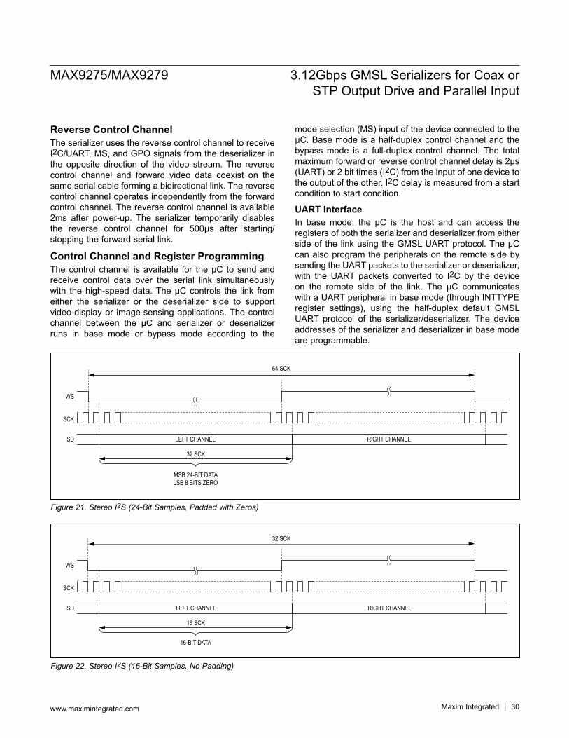
Figure 21. Stereo I2S (24-Bit Samples, Padded with Zeros)
Figure 22. Stereo I2S (16-Bit Samples, No Padding)
32 SCK
WS
SCK
SD
64 SCK
LEFT CHANNEL
MSB 24-BIT DATALSB 8 BITS ZERO
RIGHT CHANNEL
WS
SCK
SD
32 SCK
LEFT CHANNEL
16-BIT DATA
RIGHT CHANNEL
16 SCK
MAX9275/MAX9279 3.12Gbps GMSL Serializers for Coax or STP Output Drive and Parallel Input
www.maximintegrated.com Maxim Integrated 31
When the peripheral interface is I2C, the serializer/deserializer converts UART packets to I2C that have device addresses different from those of the serializer or deserializer. The converted I2C bit rate is the same as the original UART bit rate.The deserializer uses differential line coding to send signals over the reverse channel to the serializer. The bit rate of the control channel is 9.6kbps to 1Mbps in both directions. The serializer and deserializer automatically detect the control-channel bit rate in base mode. Packet bit rate changes can be made in steps of
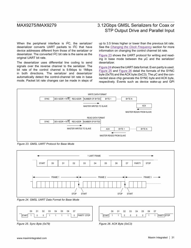
up to 3.5 times higher or lower than the previous bit rate. See the Changing the Clock Frequency section for more information on changing the control channel bit rate.Figure 23 shows the UART protocol for writing and read-ing in base mode between the µC and the serializer/deserializer.Figure 24 shows the UART data format. Even parity is used. Figure 25 and Figure 26 detail the formats of the SYNC byte (0x79) and the ACK byte (0xC3). The µC and the con-nected slave chip generate the SYNC byte and ACK byte, respectively. Events such as device wake-up and GPI
Figure 23. GMSL UART Protocol for Base Mode
Figure 24. GMSL UART Data Format for Base Mode
Figure 25. Sync Byte (0x79) Figure 26. ACK Byte (0xC3)
WRITE DATA FORMAT
SYNC REG ADDR NUMBER OF BYTES
SYNC DEV ADDR + R/W REG ADDR NUMBER OF BYTES BYTE 1 BYTE N
ACK
BYTE NBYTE 1ACK
MASTER READS FROM SLAVE
READ DATA FORMAT
MASTER WRITES TO SLAVE
MASTER WRITES TO SLAVE
MASTER READS FROM SLAVE
DEV ADDR + R/W
START D0 D1 D2 D3 D4 D5 D6 D7 PARITY STOP
1 UART FRAME
FRAME 1 FRAME 2 FRAME 3
STOP START STOP START
START
D0
1 0 0 1 1 1 1 0
D1 D2 D3 D4 D5 D6 D7
PARITY STOP START
D0
1 1 0 0 0 0 1 1
D1 D2 D3 D4 D5 D6 D7
PARITY STOP
MAX9275/MAX9279 3.12Gbps GMSL Serializers for Coax or STP Output Drive and Parallel Input
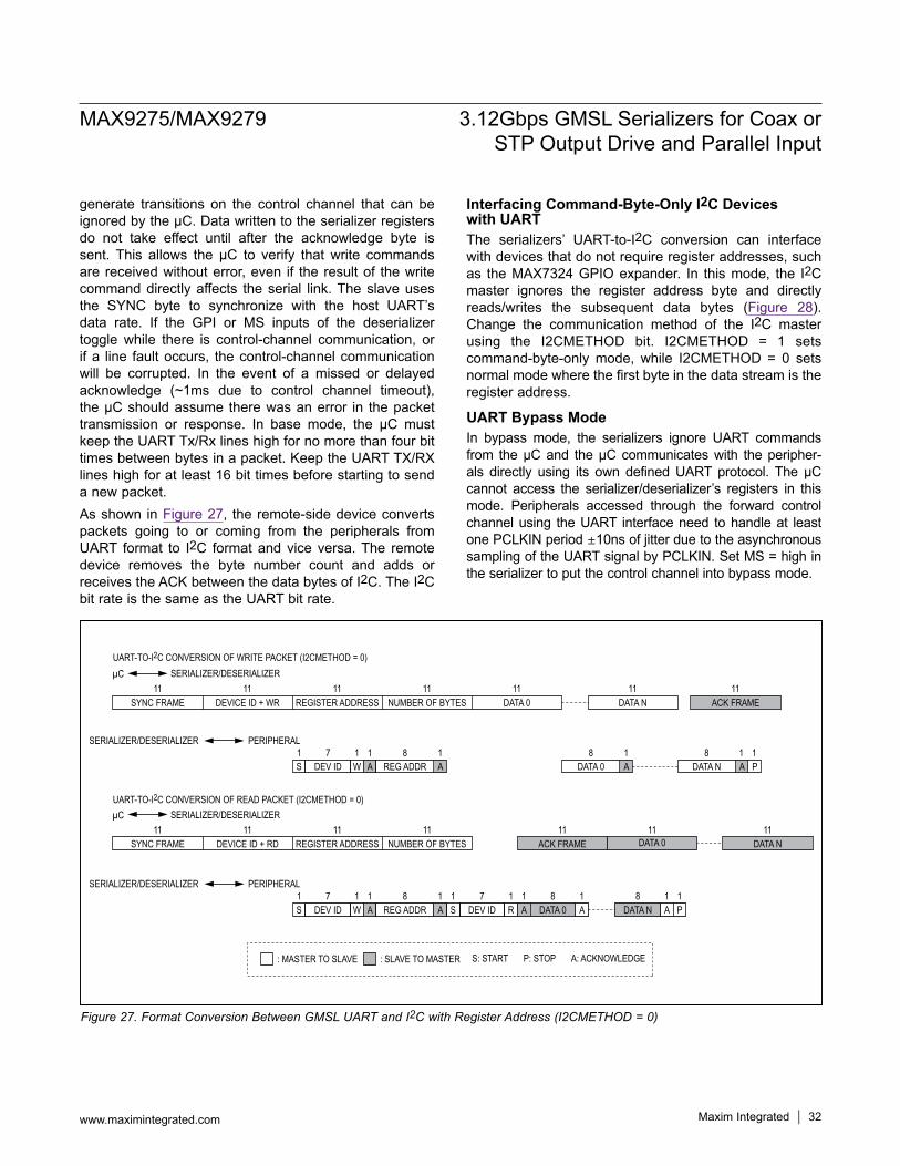
www.maximintegrated.com Maxim Integrated 32
generate transitions on the control channel that can be ignored by the µC. Data written to the serializer registers do not take effect until after the acknowledge byte is sent. This allows the µC to verify that write commands are received without error, even if the result of the write command directly affects the serial link. The slave uses the SYNC byte to synchronize with the host UART’s data rate. If the GPI or MS inputs of the deserializer toggle while there is control-channel communication, or if a line fault occurs, the control-channel communication will be corrupted. In the event of a missed or delayed acknowledge (~1ms due to control channel timeout), the µC should assume there was an error in the packet transmission or response. In base mode, the µC must keep the UART Tx/Rx lines high for no more than four bit times between bytes in a packet. Keep the UART TX/RX lines high for at least 16 bit times before starting to send a new packet.As shown in Figure 27, the remote-side device converts packets going to or coming from the peripherals from UART format to I2C format and vice versa. The remote device removes the byte number count and adds or receives the ACK between the data bytes of I2C. The I2C bit rate is the same as the UART bit rate.
Interfacing Command-Byte-Only I2C Devices with UARTThe serializers’ UART-to-I2C conversion can interface with devices that do not require register addresses, such as the MAX7324 GPIO expander. In this mode, the I2C master ignores the register address byte and directly reads/writes the subsequent data bytes (Figure 28). Change the communication method of the I2C master using the I2CMETHOD bit. I2CMETHOD = 1 sets command-byte-only mode, while I2CMETHOD = 0 sets normal mode where the first byte in the data stream is the register address.
UART Bypass ModeIn bypass mode, the serializers ignore UART commands from the µC and the µC communicates with the peripher-als directly using its own defined UART protocol. The µC cannot access the serializer/deserializer’s registers in this mode. Peripherals accessed through the forward control channel using the UART interface need to handle at least one PCLKIN period ±10ns of jitter due to the asynchronous sampling of the UART signal by PCLKIN. Set MS = high in the serializer to put the control channel into bypass mode.
Figure 27. Format Conversion Between GMSL UART and I2C with Register Address (I2CMETHOD = 0)
11SYNC FRAME REGISTER ADDRESS NUMBER OF BYTESDEVICE ID + WR DATA 0
DEV ID A
11 11 11 11DATA N
11 11
S1 11
ACK FRAME
7
: MASTER TO SLAVE
8
SERIALIZER/DESERIALIZER PERIPHERAL
W1
REG ADDR8
A1 1 8 1
11SYNC FRAME REGISTER ADDRESS NUMBER OF BYTESDEVICE ID + RD
11 11 11 11ACK FRAME DATA 0
11DATA N
11
UART-TO-I2C CONVERSION OF WRITE PACKET (I2CMETHOD = 0)
UART-TO-I2C CONVERSION OF READ PACKET (I2CMETHOD = 0)
S: START P: STOP A: ACKNOWLEDGE: SLAVE TO MASTER
DATA 0 A DATA N A P
DEV ID AS1 17
W1
DEV ID AS1 17
R1
DATA N P18
A1
DATA 08
A1
REG ADDR8
A1
µC SERIALIZER/DESERIALIZER
µC SERIALIZER/DESERIALIZER
SERIALIZER/DESERIALIZER PERIPHERAL
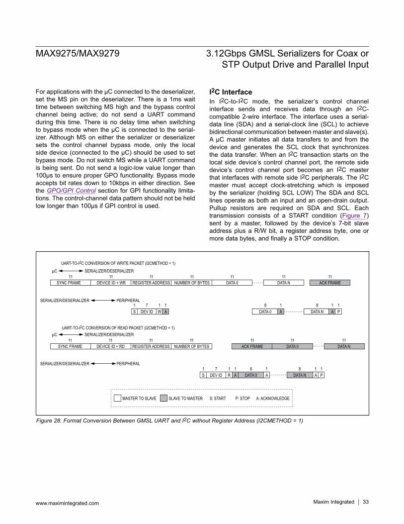
MAX9275/MAX9279 3.12Gbps GMSL Serializers for Coax or STP Output Drive and Parallel Input
www.maximintegrated.com Maxim Integrated 33
For applications with the µC connected to the deserializer, set the MS pin on the deserializer. There is a 1ms wait time between switching MS high and the bypass control channel being active; do not send a UART command during this time. There is no delay time when switching to bypass mode when the µC is connected to the serial-izer. Although MS on either the serializer or deserializer sets the control channel bypass mode, only the local side device (connected to the µC) should be used to set bypass mode. Do not switch MS while a UART command is being sent. Do not send a logic-low value longer than 100µs to ensure proper GPO functionality. Bypass mode accepts bit rates down to 10kbps in either direction. See the GPO/GPI Control section for GPI functionality limita-tions. The control-channel data pattern should not be held low longer than 100µs if GPI control is used.
I2C InterfaceIn I2C-to-I2C mode, the serializer’s control channel interface sends and receives data through an I2C-compatible 2-wire interface. The interface uses a serial-data line (SDA) and a serial-clock line (SCL) to achieve bidirectional communication between master and slave(s). A µC master initiates all data transfers to and from the device and generates the SCL clock that synchronizes the data transfer. When an I2C transaction starts on the local side device’s control channel port, the remote side device’s control channel port becomes an I2C master that interfaces with remote side I2C peripherals. The I2C master must accept clock-stretching which is imposed by the serializer (holding SCL LOW) The SDA and SCL lines operate as both an input and an open-drain output. Pullup resistors are required on SDA and SCL. Each transmission consists of a START condition (Figure 7) sent by a master, followed by the device’s 7-bit slave address plus a R/W bit, a register address byte, one or more data bytes, and finally a STOP condition.
Figure 28. Format Conversion Between GMSL UART and I2C without Register Address (I2CMETHOD = 1)
MASTER TO SLAVE
SERIALIZER/DESERIALIZER
SERIALIZER/DESERIALIZER
SERIALIZER/DESERIALIZERUART-TO-I2C CONVERSION OF READ PACKET (I2CMETHOD = 1)
UART-TO-I2C CONVERSION OF WRITE PACKET (I2CMETHOD = 1)
µC
SERIALIZER/DESERIALIZERµC
SYNC FRAME
11 11 11 11 11 11 11
1111 11 11 11 11 11DEVICE ID + RD REGISTER ADDRESS NUMBER OF BYTES
SYNC FRAME DEVICE ID + WR REGISTER ADDRESS NUMBER OF BYTES DATA 0 DATA N ACK FRAME
ACK FRAME DATA 0 DATA N
DATA NADATA 0W ADEV IDS A P
PERIPHERAL
PERIPHERAL
S1 1 1 8
8 81111 7 1 1
81 1 17DEV ID R A A A PDATA 0 DATA N
SLAVE TO MASTER S: START P: STOP A: ACKNOWLEDGE
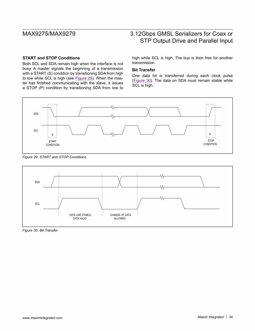
MAX9275/MAX9279 3.12Gbps GMSL Serializers for Coax or STP Output Drive and Parallel Input
www.maximintegrated.com Maxim Integrated 34
START and STOP ConditionsBoth SCL and SDA remain high when the interface is not busy. A master signals the beginning of a transmission with a START (S) condition by transitioning SDA from high to low while SCL is high (see Figure 29). When the mas-ter has finished communicating with the slave, it issues a STOP (P) condition by transitioning SDA from low to
high while SCL is high. The bus is then free for another transmission.
Bit TransferOne data bit is transferred during each clock pulse (Figure 30). The data on SDA must remain stable while SCL is high.
Figure 29. START and STOP Conditions
Figure 30. Bit Transfer
SDA
SCL
DATA LINE STABLE;DATA VALID
CHANGE OF DATAALLOWED
SDA
SCL
START CONDITION
STOPCONDITION
S P
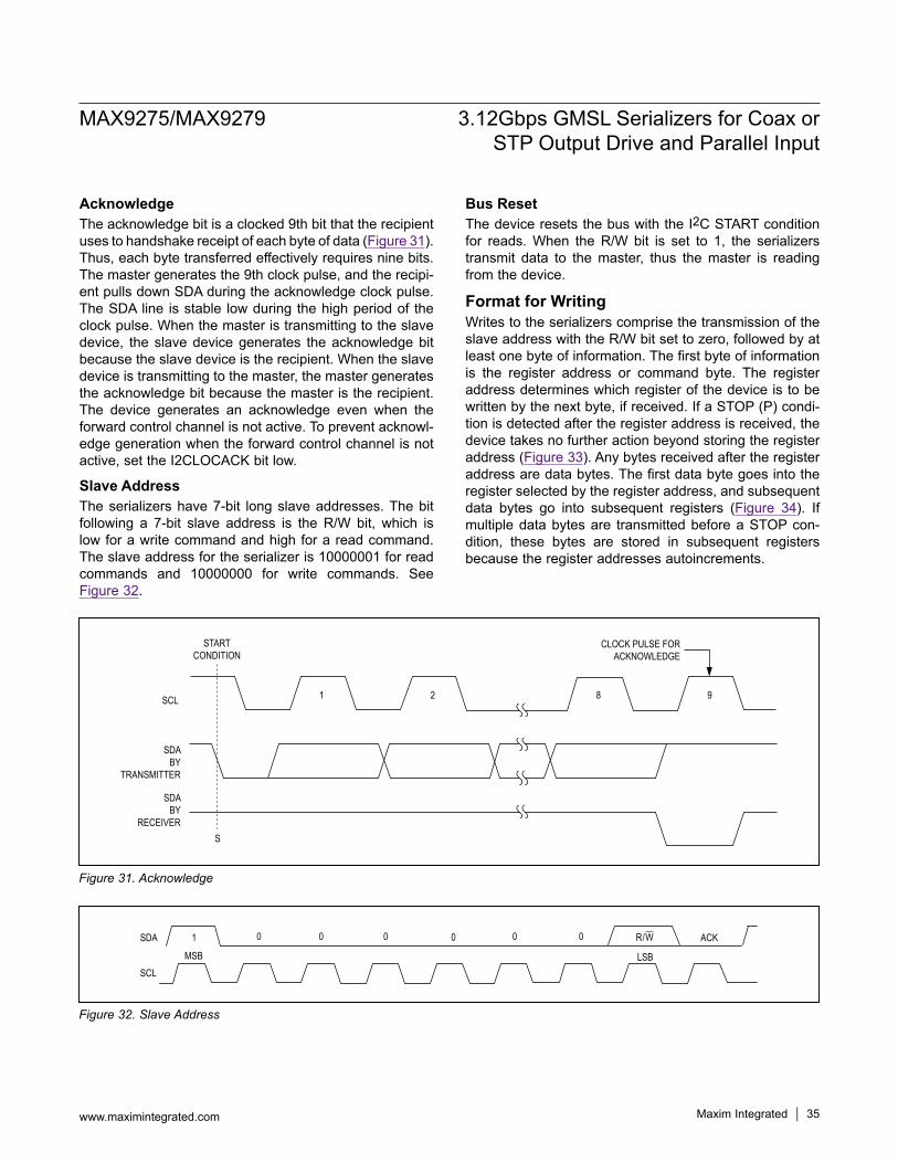
MAX9275/MAX9279 3.12Gbps GMSL Serializers for Coax or STP Output Drive and Parallel Input
www.maximintegrated.com Maxim Integrated 35
AcknowledgeThe acknowledge bit is a clocked 9th bit that the recipient uses to handshake receipt of each byte of data (Figure 31). Thus, each byte transferred effectively requires nine bits. The master generates the 9th clock pulse, and the recipi-ent pulls down SDA during the acknowledge clock pulse. The SDA line is stable low during the high period of the clock pulse. When the master is transmitting to the slave device, the slave device generates the acknowledge bit because the slave device is the recipient. When the slave device is transmitting to the master, the master generates the acknowledge bit because the master is the recipient. The device generates an acknowledge even when the forward control channel is not active. To prevent acknowl-edge generation when the forward control channel is not active, set the I2CLOCACK bit low.
Slave AddressThe serializers have 7-bit long slave addresses. The bit following a 7-bit slave address is the R/W bit, which is low for a write command and high for a read command. The slave address for the serializer is 10000001 for read commands and 10000000 for write commands. See Figure 32.
Bus ResetThe device resets the bus with the I2C START condition for reads. When the R/W bit is set to 1, the serializers transmit data to the master, thus the master is reading from the device.
Format for WritingWrites to the serializers comprise the transmission of the slave address with the R/W bit set to zero, followed by at least one byte of information. The first byte of information is the register address or command byte. The register address determines which register of the device is to be written by the next byte, if received. If a STOP (P) condi-tion is detected after the register address is received, the device takes no further action beyond storing the register address (Figure 33). Any bytes received after the register address are data bytes. The first data byte goes into the register selected by the register address, and subsequent data bytes go into subsequent registers (Figure 34). If multiple data bytes are transmitted before a STOP con-dition, these bytes are stored in subsequent registers because the register addresses autoincrements.
Figure 31. Acknowledge
Figure 32. Slave Address
SCL
SDABY
TRANSMITTER
CLOCK PULSE FORACKNOWLEDGE
START CONDITION
SDABY
RECEIVER
1 2 8 9
S
SDA 0 ACK
SCLMSB LSB
1 0 R/W0 0 0 0
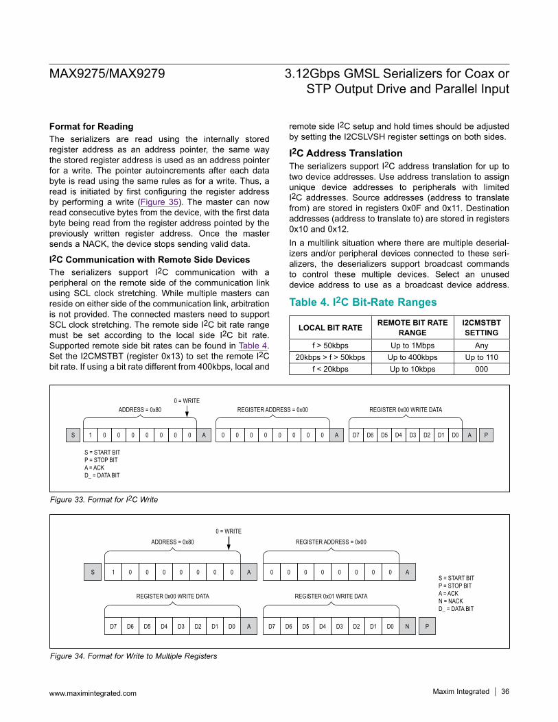
MAX9275/MAX9279 3.12Gbps GMSL Serializers for Coax or STP Output Drive and Parallel Input
www.maximintegrated.com Maxim Integrated 36
Format for ReadingThe serializers are read using the internally stored register address as an address pointer, the same way the stored register address is used as an address pointer for a write. The pointer autoincrements after each data byte is read using the same rules as for a write. Thus, a read is initiated by first configuring the register address by performing a write (Figure 35). The master can now read consecutive bytes from the device, with the first data byte being read from the register address pointed by the previously written register address. Once the master sends a NACK, the device stops sending valid data.
I2C Communication with Remote Side DevicesThe serializers support I2C communication with a peripheral on the remote side of the communication link using SCL clock stretching. While multiple masters can reside on either side of the communication link, arbitration is not provided. The connected masters need to support SCL clock stretching. The remote side I2C bit rate range must be set according to the local side I2C bit rate. Supported remote side bit rates can be found in Table 4. Set the I2CMSTBT (register 0x13) to set the remote I2C bit rate. If using a bit rate different from 400kbps, local and
remote side I2C setup and hold times should be adjusted by setting the I2CSLVSH register settings on both sides.
I2C Address TranslationThe serializers support I2C address translation for up to two device addresses. Use address translation to assign unique device addresses to peripherals with limited I2C addresses. Source addresses (address to translate from) are stored in registers 0x0F and 0x11. Destination addresses (address to translate to) are stored in registers 0x10 and 0x12.In a multilink situation where there are multiple deserial-izers and/or peripheral devices connected to these seri-alizers, the deserializers support broadcast commands to control these multiple devices. Select an unused device address to use as a broadcast device address.
Figure 33. Format for I2C Write
Figure 34. Format for Write to Multiple Registers
Table 4. I2C Bit-Rate Ranges
S 1 0 0 0
ADDRESS = 0x800 = WRITE
0 0 0 0 A 0 0 0 0
REGISTER ADDRESS = 0x00
0 0 0 0 A PD7 D6 D5 D4
REGISTER 0x00 WRITE DATA
D3 D2 D1 D0 A
S = START BITP = STOP BITA = ACKD_ = DATA BIT
S = START BITP = STOP BITA = ACKN = NACKD_ = DATA BIT
S 1 0 0 0
ADDRESS = 0x800 = WRITE
0 0 0 0 A 0 0 0 0
REGISTER ADDRESS = 0x00
0 0 0 0 A
D7 D6 D5 D4
REGISTER 0x00 WRITE DATA
D3 D2 D1 D0 A D7 PD6 D5 D4
REGISTER 0x01 WRITE DATA
D3 D2 D1 D0 N
LOCAL BIT RATE REMOTE BIT RATE RANGE
I2CMSTBT SETTING
f > 50kbps Up to 1Mbps Any20kbps > f > 50kbps Up to 400kbps Up to 110
f < 20kbps Up to 10kbps 000
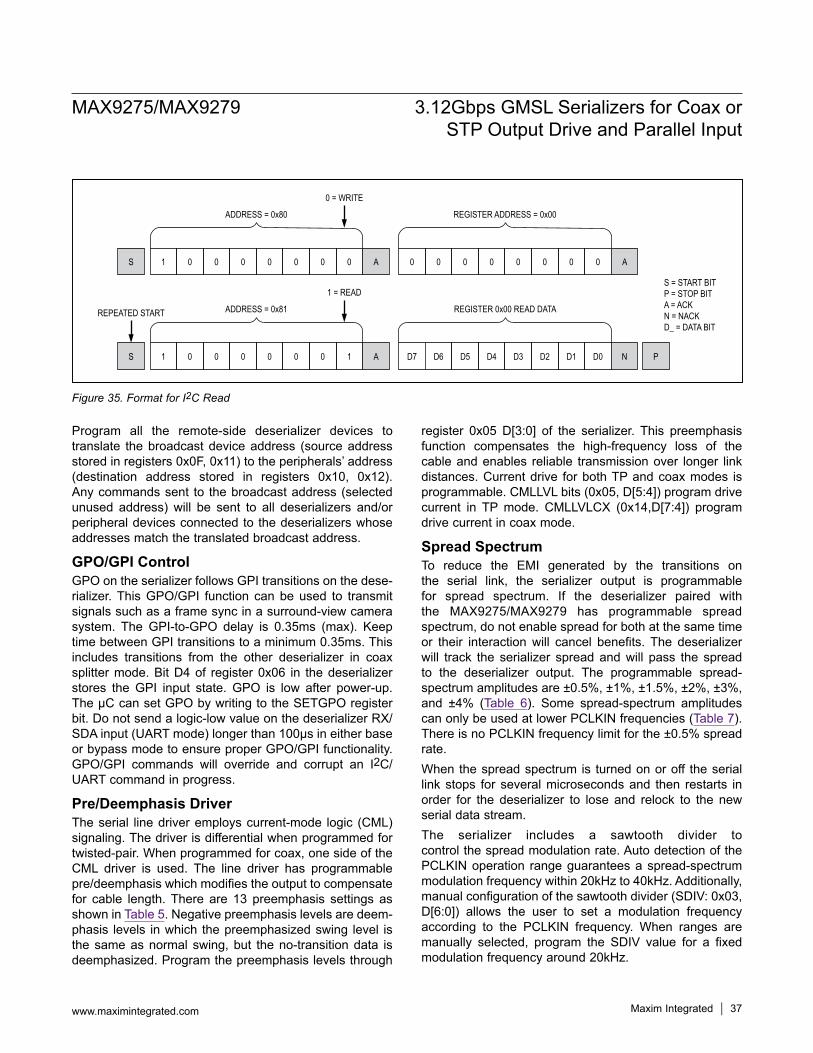
MAX9275/MAX9279 3.12Gbps GMSL Serializers for Coax or STP Output Drive and Parallel Input
www.maximintegrated.com Maxim Integrated 37
Program all the remote-side deserializer devices to translate the broadcast device address (source address stored in registers 0x0F, 0x11) to the peripherals’ address (destination address stored in registers 0x10, 0x12). Any commands sent to the broadcast address (selected unused address) will be sent to all deserializers and/or peripheral devices connected to the deserializers whose addresses match the translated broadcast address.
GPO/GPI ControlGPO on the serializer follows GPI transitions on the dese-rializer. This GPO/GPI function can be used to transmit signals such as a frame sync in a surround-view camera system. The GPI-to-GPO delay is 0.35ms (max). Keep time between GPI transitions to a minimum 0.35ms. This includes transitions from the other deserializer in coax splitter mode. Bit D4 of register 0x06 in the deserializer stores the GPI input state. GPO is low after power-up. The µC can set GPO by writing to the SETGPO register bit. Do not send a logic-low value on the deserializer RX/SDA input (UART mode) longer than 100µs in either base or bypass mode to ensure proper GPO/GPI functionality. GPO/GPI commands will override and corrupt an I2C/UART command in progress.
Pre/Deemphasis DriverThe serial line driver employs current-mode logic (CML) signaling. The driver is differential when programmed for twisted-pair. When programmed for coax, one side of the CML driver is used. The line driver has programmable pre/deemphasis which modifies the output to compensate for cable length. There are 13 preemphasis settings as shown in Table 5. Negative preemphasis levels are deem-phasis levels in which the preemphasized swing level is the same as normal swing, but the no-transition data is deemphasized. Program the preemphasis levels through
register 0x05 D[3:0] of the serializer. This preemphasis function compensates the high-frequency loss of the cable and enables reliable transmission over longer link distances. Current drive for both TP and coax modes is programmable. CMLLVL bits (0x05, D[5:4]) program drive current in TP mode. CMLLVLCX (0x14,D[7:4]) program drive current in coax mode.
Spread SpectrumTo reduce the EMI generated by the transitions on the serial link, the serializer output is programmable for spread spectrum. If the deserializer paired with the MAX9275/MAX9279 has programmable spread spectrum, do not enable spread for both at the same time or their interaction will cancel benefits. The deserializer will track the serializer spread and will pass the spread to the deserializer output. The programmable spread-spectrum amplitudes are ±0.5%, ±1%, ±1.5%, ±2%, ±3%, and ±4% (Table 6). Some spread-spectrum amplitudes can only be used at lower PCLKIN frequencies (Table 7). There is no PCLKIN frequency limit for the ±0.5% spread rate.When the spread spectrum is turned on or off the serial link stops for several microseconds and then restarts in order for the deserializer to lose and relock to the new serial data stream.The serializer includes a sawtooth divider to control the spread modulation rate. Auto detection of the PCLKIN operation range guarantees a spread-spectrum modulation frequency within 20kHz to 40kHz. Additionally, manual configuration of the sawtooth divider (SDIV: 0x03, D[6:0]) allows the user to set a modulation frequency according to the PCLKIN frequency. When ranges are manually selected, program the SDIV value for a fixed modulation frequency around 20kHz.
Figure 35. Format for I2C Read
S = START BITP = STOP BITA = ACKN = NACKD_ = DATA BIT
S
S
1 0 0 0
ADDRESS = 0x80
0 = WRITE
0 0 0 0 A
1 = READ
REPEATED START
0 0 0 0
REGISTER ADDRESS = 0x00
0 0 0 0 A
1 0 0 0
ADDRESS = 0x81
0 0 0 1 A D7 PD6 D5 D4
REGISTER 0x00 READ DATA
D3 D2 D1 D0 N
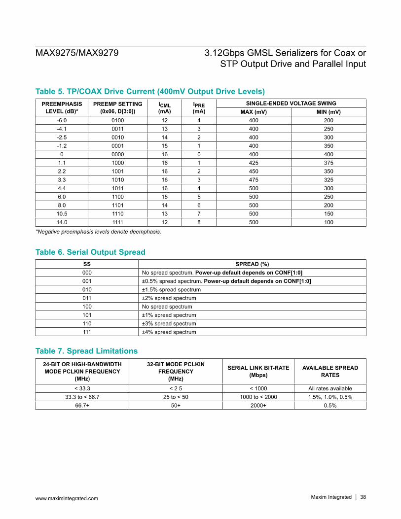
*Negative preemphasis levels denote deemphasis.
MAX9275/MAX9279 3.12Gbps GMSL Serializers for Coax or STP Output Drive and Parallel Input
www.maximintegrated.com Maxim Integrated 38
Table 5. TP/COAX Drive Current (400mV Output Drive Levels)
Table 6. Serial Output Spread
Table 7. Spread Limitations
SS SPREAD (%)000 No spread spectrum. Power-up default depends on CONF[1:0]001 ±0.5% spread spectrum. Power-up default depends on CONF[1:0]010 ±1.5% spread spectrum011 ±2% spread spectrum100 No spread spectrum101 ±1% spread spectrum110 ±3% spread spectrum111 ±4% spread spectrum
24-BIT OR HIGH-BANDWIDTH MODE PCLKIN FREQUENCY
(MHz)
32-BIT MODE PCLKIN FREQUENCY
(MHz)
SERIAL LINK BIT-RATE(Mbps)
AVAILABLE SPREAD RATES
< 33.3 < 2 5 < 1000 All rates available33.3 to < 66.7 25 to < 50 1000 to < 2000 1.5%, 1.0%, 0.5%
66.7+ 50+ 2000+ 0.5%
PREEMPHASIS LEVEL (dB)*
PREEMP SETTING(0x06, D[3:0])
ICML(mA)
IPRE (mA)
SINGLE-ENDED VOLTAGE SWINGMAX (mV) MIN (mV)
-6.0 0100 12 4 400 200-4.1 0011 13 3 400 250-2.5 0010 14 2 400 300-1.2 0001 15 1 400 350
0 0000 16 0 400 4001.1 1000 16 1 425 3752.2 1001 16 2 450 3503.3 1010 16 3 475 3254.4 1011 16 4 500 3006.0 1100 15 5 500 2508.0 1101 14 6 500 200
10.5 1110 13 7 500 15014.0 1111 12 8 500 100
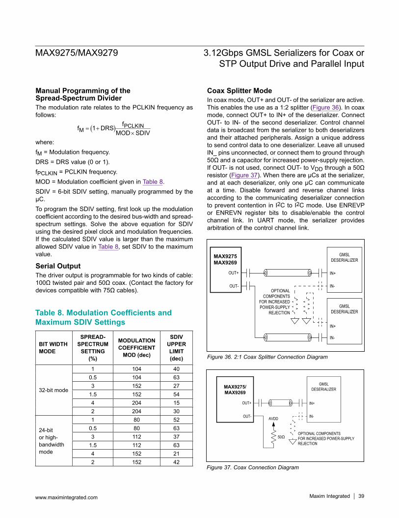
MAX9275/MAX9279 3.12Gbps GMSL Serializers for Coax or STP Output Drive and Parallel Input
www.maximintegrated.com Maxim Integrated 39
Manual Programming of the Spread-Spectrum DividerThe modulation rate relates to the PCLKIN frequency as follows:
( ) PCLKINM
ff 1 DRSMOD SDIV
= +×
where:fM = Modulation frequency.DRS = DRS value (0 or 1).fPCLKIN = PCLKIN frequency.MOD = Modulation coefficient given in Table 8.SDIV = 6-bit SDIV setting, manually programmed by the µC.To program the SDIV setting, first look up the modulation coefficient according to the desired bus-width and spread-spectrum settings. Solve the above equation for SDIV using the desired pixel clock and modulation frequencies. If the calculated SDIV value is larger than the maximum allowed SDIV value in Table 8, set SDIV to the maximum value.
Serial OutputThe driver output is programmable for two kinds of cable: 100Ω twisted pair and 50Ω coax. (Contact the factory for devices compatible with 75Ω cables).
Coax Splitter ModeIn coax mode, OUT+ and OUT- of the serializer are active. This enables the use as a 1:2 splitter (Figure 36). In coax mode, connect OUT+ to IN+ of the deserializer. Connect OUT- to IN- of the second deserializer. Control channel data is broadcast from the serializer to both deserializers and their attached peripherals. Assign a unique address to send control data to one deserializer. Leave all unused IN_ pins unconnected, or connect them to ground through 50Ω and a capacitor for increased power-supply rejection. If OUT- is not used, connect OUT- to VDD through a 50Ω resistor (Figure 37). When there are µCs at the serializer, and at each deserializer, only one µC can communicate at a time. Disable forward and reverse channel links according to the communicating deserializer connection to prevent contention in I2C to I2C mode. Use ENREVP or ENREVN register bits to disable/enable the control channel link. In UART mode, the serializer provides arbitration of the control channel link.
Table 8. Modulation Coefficients and Maximum SDIV Settings
Figure 36. 2:1 Coax Splitter Connection Diagram
Figure 37. Coax Connection Diagram
OUT+
OUT-OPTIONAL
COMPONENTSFOR INCREASEDPOWER-SUPPLY
REJECTION
IN+
IN-
IN+
IN-
MAX9275MAX9269
GMSLDESERIALIZER
GMSLDESERIALIZER
OUT+
OUT-
IN+
OPTIONAL COMPONENTSFOR INCREASED POWER-SUPPLYREJECTION
IN-AVDD
50Ω
MAX9275/MAX9269
GMSLDESERIALIZER
BIT WIDTH MODE
SPREAD-SPECTRUM
SETTING (%)
MODULATION COEFFICIENT
MOD (dec)
SDIV UPPER LIMIT (dec)
32-bit mode
1 104 400.5 104 633 152 27
1.5 152 544 204 152 204 30
24-bit or high-bandwidth mode
1 80 520.5 80 633 112 37
1.5 112 634 152 212 152 42
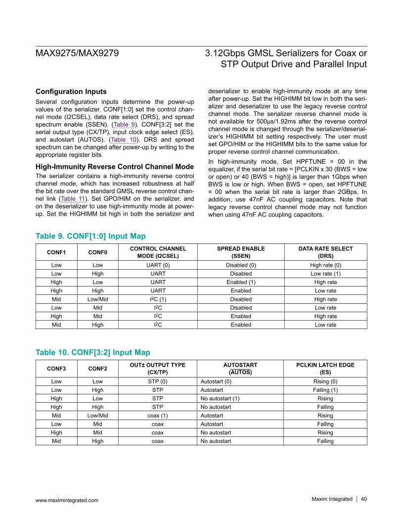
MAX9275/MAX9279 3.12Gbps GMSL Serializers for Coax or STP Output Drive and Parallel Input
www.maximintegrated.com Maxim Integrated 40
Configuration InputsSeveral configuration inputs determine the power-up values of the serializer. CONF[1:0] set the control chan-nel mode (I2CSEL), data rate select (DRS), and spread spectrum enable (SSEN). (Table 9). CONF[3:2] set the serial output type (CX/TP), input clock edge select (ES), and autostart (AUTOS). (Table 10). DRS and spread spectrum can be changed after power-up by writing to the appropriate register bits
High-Immunity Reverse Control Channel ModeThe serializer contains a high-immunity reverse control channel mode, which has increased robustness at half the bit rate over the standard GMSL reverse control chan-nel link (Table 11). Set GPO/HIM on the serializer, and on the deserializer to use high-immunity mode at power-up. Set the HIGHIMM bit high in both the serializer and
deserializer to enable high-immunity mode at any time after power-up. Set the HIGHIMM bit low in both the seri-alizer and deserializer to use the legacy reverse control channel mode. The serializer reverse channel mode is not available for 500µs/1.92ms after the reverse control channel mode is changed through the serializer/deserial-izer’s HIGHIMM bit setting respectively. The user must set GPO/HIM or the HIGHIMM bits to the same value for proper reverse control channel communication.In high-immunity mode, Set HPFTUNE = 00 in the equalizer, if the serial bit rate = [PCLKIN x 30 (BWS = low or open) or 40 (BWS = high)] is larger than 1Gbps when BWS is low or high. When BWS = open, set HPFTUNE = 00 when the serial bit rate is larger than 2GBps. In addition, use 47nF AC coupling capacitors. Note that legacy reverse control channel mode may not function when using 47nF AC coupling capacitors.
Table 9. CONF[1:0] Input Map
Table 10. CONF[3:2] Input Map
CONF1 CONF0 CONTROL CHANNEL MODE (I2CSEL)
SPREAD ENABLE(SSEN)
DATA RATE SELECT(DRS)
Low Low UART (0) Disabled (0) High rate (0)Low High UART Disabled Low rate (1)High Low UART Enabled (1) High rateHigh High UART Enabled Low rateMid Low/Mid I2C (1) Disabled High rateLow Mid I2C Disabled Low rateHigh Mid I2C Enabled High rateMid High I2C Enabled Low rate
CONF3 CONF2 OUT± OUTPUT TYPE(CX/TP)
AUTOSTART(AUTOS)
PCLKIN LATCH EDGE(ES)
Low Low STP (0) Autostart (0) Rising (0)Low High STP Autostart Falling (1)High Low STP No autostart (1) RisingHigh High STP No autostart FallingMid Low/Mid coax (1) Autostart RisingLow Mid coax Autostart FallingHigh Mid coax No autostart RisingMid High coax No autostart Falling
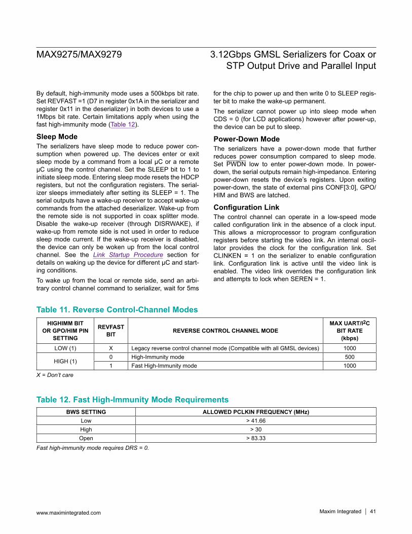
X = Don’t care
Fast high-immunity mode requires DRS = 0.
MAX9275/MAX9279 3.12Gbps GMSL Serializers for Coax or STP Output Drive and Parallel Input
www.maximintegrated.com Maxim Integrated 41
By default, high-immunity mode uses a 500kbps bit rate. Set REVFAST =1 (D7 in register 0x1A in the serializer and register 0x11 in the deserializer) in both devices to use a 1Mbps bit rate. Certain limitations apply when using the fast high-immunity mode (Table 12).
Sleep ModeThe serializers have sleep mode to reduce power con-sumption when powered up. The devices enter or exit sleep mode by a command from a local µC or a remote µC using the control channel. Set the SLEEP bit to 1 to initiate sleep mode. Entering sleep mode resets the HDCP registers, but not the configuration registers. The serial-izer sleeps immediately after setting its SLEEP = 1. The serial outputs have a wake-up receiver to accept wake-up commands from the attached deserializer. Wake-up from the remote side is not supported in coax splitter mode. Disable the wake-up receiver (through DISRWAKE), if wake-up from remote side is not used in order to reduce sleep mode current. If the wake-up receiver is disabled, the device can only be woken up from the local control channel. See the Link Startup Procedure section for details on waking up the device for different µC and start-ing conditions.To wake up from the local or remote side, send an arbi-trary control channel command to serializer, wait for 5ms
for the chip to power up and then write 0 to SLEEP regis-ter bit to make the wake-up permanent.The serializer cannot power up into sleep mode when CDS = 0 (for LCD applications) however after power-up, the device can be put to sleep.
Power-Down ModeThe serializers have a power-down mode that further reduces power consumption compared to sleep mode. Set PWDN low to enter power-down mode. In power-down, the serial outputs remain high-impedance. Entering power-down resets the device’s registers. Upon exiting power-down, the state of external pins CONF[3:0], GPO/HIM and BWS are latched.
Configuration LinkThe control channel can operate in a low-speed mode called configuration link in the absence of a clock input. This allows a microprocessor to program configuration registers before starting the video link. An internal oscil-lator provides the clock for the configuration link. Set CLINKEN = 1 on the serializer to enable configuration link. Configuration link is active until the video link is enabled. The video link overrides the configuration link and attempts to lock when SEREN = 1.
Table 11. Reverse Control-Channel Modes
Table 12. Fast High-Immunity Mode Requirements
HIGHIMM BIT OR GPO/HIM PIN
SETTING
REVFAST BIT REVERSE CONTROL CHANNEL MODE
MAX UART/I2C BIT RATE
(kbps)LOW (1) X Legacy reverse control channel mode (Compatible with all GMSL devices) 1000
HIGH (1)0 High-Immunity mode 5001 Fast High-Immunity mode 1000
BWS SETTING ALLOWED PCLKIN FREQUENCY (MHz)Low > 41.66High > 30Open > 83.33
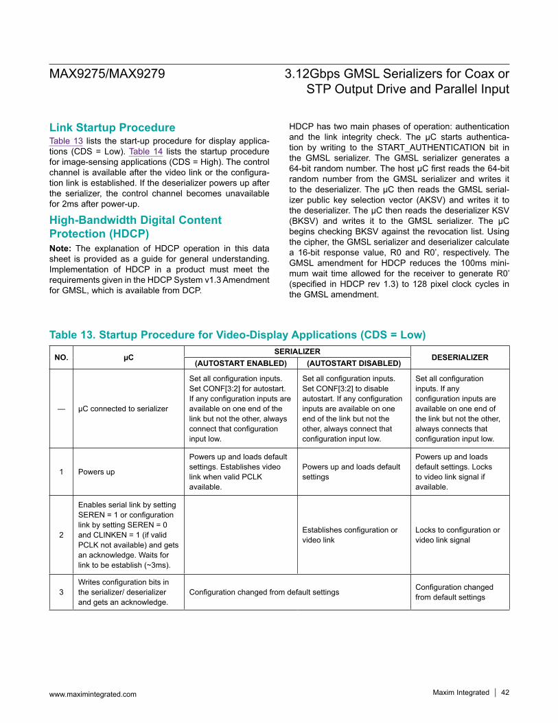
MAX9275/MAX9279 3.12Gbps GMSL Serializers for Coax or STP Output Drive and Parallel Input
www.maximintegrated.com Maxim Integrated 42
Link Startup ProcedureTable 13 lists the start-up procedure for display applica-tions (CDS = Low). Table 14 lists the startup procedure for image-sensing applications (CDS = High). The control channel is available after the video link or the configura-tion link is established. If the deserializer powers up after the serializer, the control channel becomes unavailable for 2ms after power-up.
High-Bandwidth Digital Content Protection (HDCP)Note: The explanation of HDCP operation in this data sheet is provided as a guide for general understanding. Implementation of HDCP in a product must meet the requirements given in the HDCP System v1.3 Amendment for GMSL, which is available from DCP.
HDCP has two main phases of operation: authentication and the link integrity check. The µC starts authentica-tion by writing to the START_AUTHENTICATION bit in the GMSL serializer. The GMSL serializer generates a 64-bit random number. The host µC first reads the 64-bit random number from the GMSL serializer and writes it to the deserializer. The µC then reads the GMSL serial-izer public key selection vector (AKSV) and writes it to the deserializer. The µC then reads the deserializer KSV (BKSV) and writes it to the GMSL serializer. The µC begins checking BKSV against the revocation list. Using the cipher, the GMSL serializer and deserializer calculate a 16-bit response value, R0 and R0’, respectively. The GMSL amendment for HDCP reduces the 100ms mini-mum wait time allowed for the receiver to generate R0’ (specified in HDCP rev 1.3) to 128 pixel clock cycles in the GMSL amendment.
Table 13. Startup Procedure for Video-Display Applications (CDS = Low)
NO. µCSERIALIZER
DESERIALIZER(AUTOSTART ENABLED) (AUTOSTART DISABLED)
— µC connected to serializer
Set all configuration inputs. Set CONF[3:2] for autostart. If any configuration inputs are available on one end of the link but not the other, always connect that configuration input low.
Set all configuration inputs. Set CONF[3:2] to disable autostart. If any configuration inputs are available on one end of the link but not the other, always connect that configuration input low.
Set all configuration inputs. If any configuration inputs are available on one end of the link but not the other, always connects that configuration input low.
1 Powers up
Powers up and loads default settings. Establishes video link when valid PCLK available.
Powers up and loads default settings
Powers up and loads default settings. Locks to video link signal if available.
2
Enables serial link by setting SEREN = 1 or configuration link by setting SEREN = 0 and CLINKEN = 1 (if valid PCLK not available) and gets an acknowledge. Waits for link to be establish (~3ms).
Establishes configuration or video link
Locks to configuration or video link signal
3Writes configuration bits in the serializer/ deserializer and gets an acknowledge.
Configuration changed from default settings Configuration changed from default settings
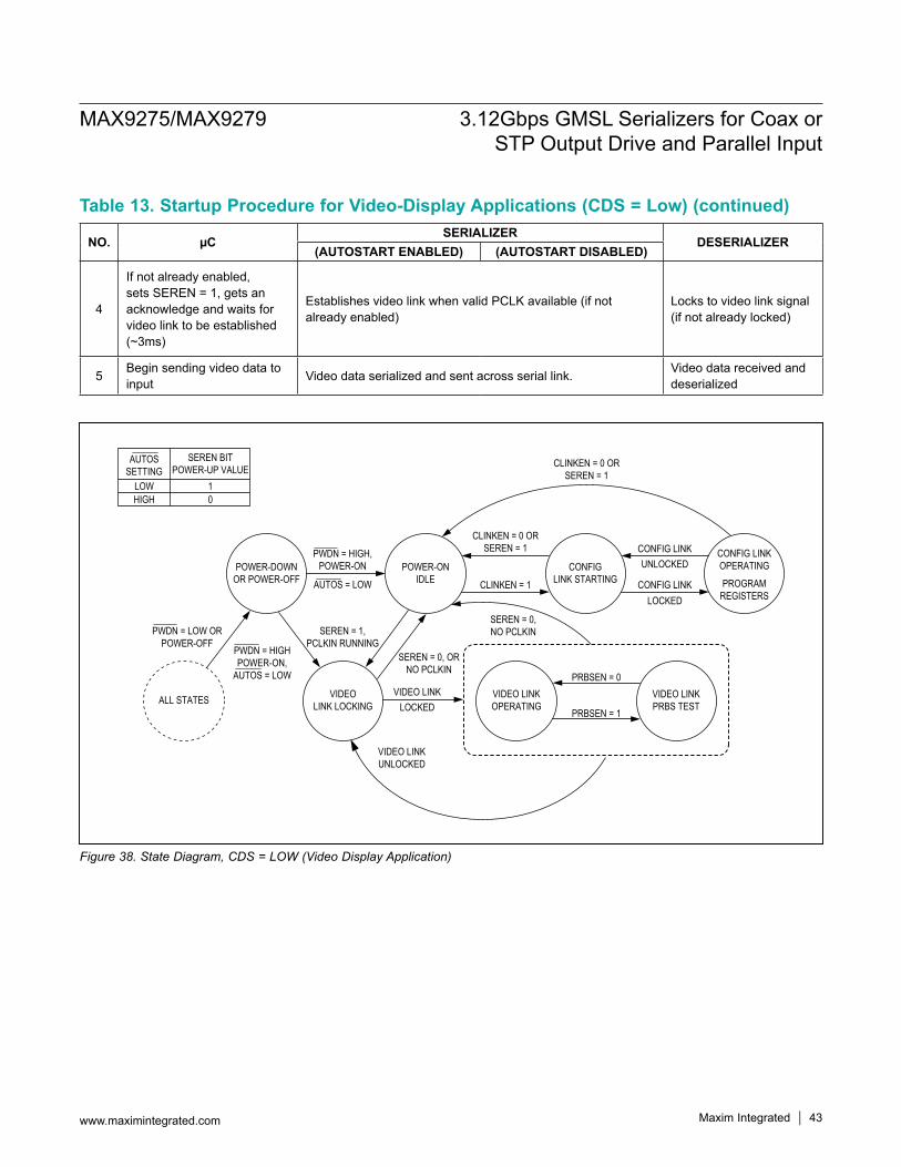
MAX9275/MAX9279 3.12Gbps GMSL Serializers for Coax or STP Output Drive and Parallel Input
www.maximintegrated.com Maxim Integrated 43
Figure 38. State Diagram, CDS = LOW (Video Display Application)
Table 13. Startup Procedure for Video-Display Applications (CDS = Low) (continued)
POWER-DOWNOR POWER-OFF
POWER-ONIDLE
CONFIG LINKOPERATING
ALL STATES VIDEOLINK LOCKING
VIDEO LINKUNLOCKED
AUTOSSETTING
LOWHIGH
10
SEREN BITPOWER-UP VALUE
PWDN = LOW ORPOWER-OFF
SEREN = 1,PCLKIN RUNNING
SEREN = 0, ORNO PCLKIN
SEREN = 0,NO PCLKIN
PWDN = HIGHPOWER-ON,
AUTOS = LOW
CONFIGLINK STARTING PROGRAM
REGISTERS
VIDEO LINKOPERATING
PRBSEN = 0
PRBSEN = 1
VIDEO LINKPRBS TEST
CLINKEN = 0 ORSEREN = 1
CLINKEN = 1
CLINKEN = 0 ORSEREN = 1
CONFIG LINKUNLOCKED
VIDEO LINKLOCKED
LOCKEDCONFIG LINK
PWDN = HIGH,POWER-ON
AUTOS = LOW
NO. µCSERIALIZER
DESERIALIZER(AUTOSTART ENABLED) (AUTOSTART DISABLED)
4
If not already enabled, sets SEREN = 1, gets an acknowledge and waits for video link to be established (~3ms)
Establishes video link when valid PCLK available (if not already enabled)
Locks to video link signal (if not already locked)
5 Begin sending video data to input Video data serialized and sent across serial link. Video data received and
deserialized
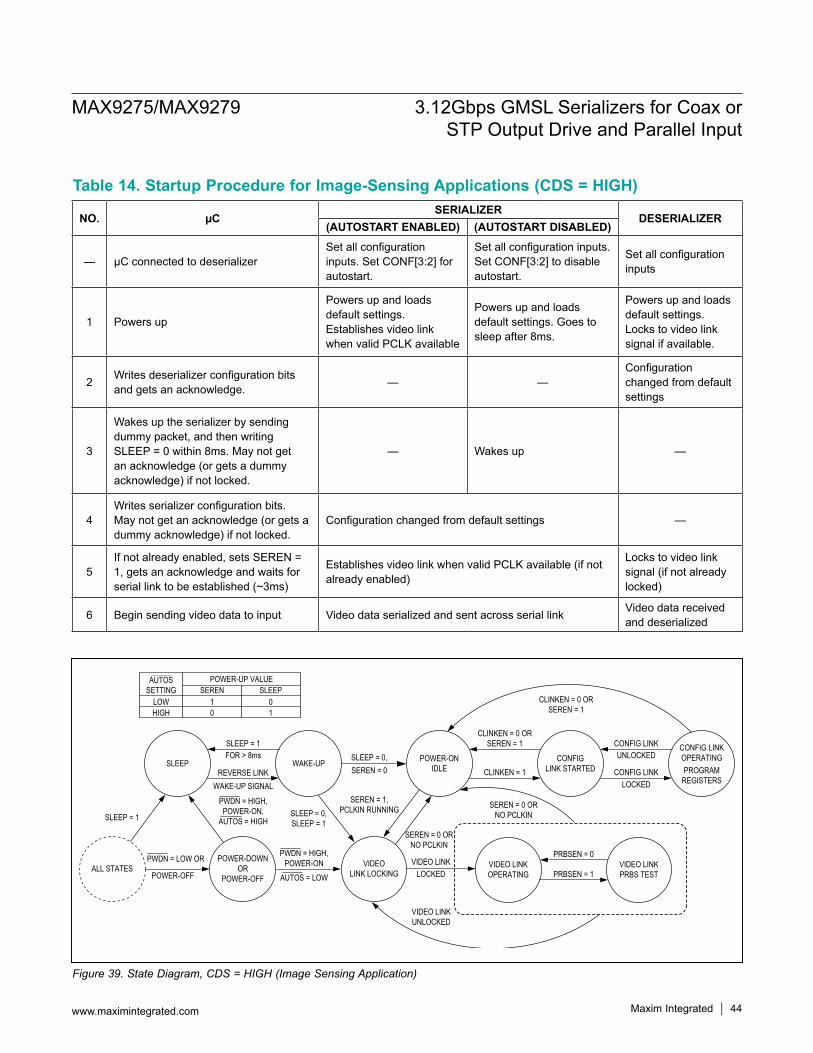
MAX9275/MAX9279 3.12Gbps GMSL Serializers for Coax or STP Output Drive and Parallel Input
www.maximintegrated.com Maxim Integrated 44
Figure 39. State Diagram, CDS = HIGH (Image Sensing Application)
Table 14. Startup Procedure for Image-Sensing Applications (CDS = HIGH)
LOWHIGH
10
0SEREN SLEEP
1
POWER-UP VALUE
SEREN = 0
FOR > 8ms
VIDEO LINKOPERATING
VIDEO LINKPRBS TEST
WAKE-UP
SLEEP = 1
WAKE-UP SIGNALREVERSE LINK
CONFIGLINK STARTED
CLINKEN = 0 ORSEREN = 1
CLINKEN = 1
UNLOCKED
LOCKED
CONFIG LINK
CONFIG LINK
SLEEP = 0,SLEEP POWER-ON
IDLE
POWER-OFFALL STATES
PWDN = LOW OR
SLEEP = 1
POWER-DOWNOR
POWER-OFF AUTOS = LOW
PWDN = HIGH,POWER-ON VIDEO
LINK LOCKING
AUTOSSETTING
CONFIG LINKOPERATINGPROGRAM
REGISTERS
CLINKEN = 0 ORSEREN = 1
VIDEO LINKLOCKED
VIDEO LINKUNLOCKED
PRBSEN = 0
PRBSEN = 1
SEREN = 1,PCLKIN RUNNING
SEREN = 0 ORNO PCLKIN
SEREN = 0 ORNO PCLKIN
PWDN = HIGH,POWER-ON,
AUTOS = HIGHSLEEP = 0,SLEEP = 1
NO. µCSERIALIZER
DESERIALIZER(AUTOSTART ENABLED) (AUTOSTART DISABLED)
— µC connected to deserializerSet all configuration inputs. Set CONF[3:2] for autostart.
Set all configuration inputs. Set CONF[3:2] to disable autostart.
Set all configuration inputs
1 Powers up
Powers up and loads default settings. Establishes video link when valid PCLK available
Powers up and loads default settings. Goes to sleep after 8ms.
Powers up and loads default settings. Locks to video link signal if available.
2 Writes deserializer configuration bits and gets an acknowledge. — —
Configuration changed from default settings
3
Wakes up the serializer by sending dummy packet, and then writing SLEEP = 0 within 8ms. May not get an acknowledge (or gets a dummy acknowledge) if not locked.
— Wakes up —
4Writes serializer configuration bits. May not get an acknowledge (or gets a dummy acknowledge) if not locked.
Configuration changed from default settings —
5If not already enabled, sets SEREN = 1, gets an acknowledge and waits for serial link to be established (~3ms)
Establishes video link when valid PCLK available (if not already enabled)
Locks to video link signal (if not already locked)
6 Begin sending video data to input Video data serialized and sent across serial link Video data received and deserialized
MAX9275/MAX9279 3.12Gbps GMSL Serializers for Coax or STP Output Drive and Parallel Input
www.maximintegrated.com Maxim Integrated 45
There are two response-value comparison modes: internal comparison and µC comparison. Set EN_INT_COMP = 1 to select internal comparison mode. Set EN_INT_COMP = 0 to select µC comparison mode. In internal compari-son mode, the µC reads the deserializer response R0’ and writes it to the GMSL serializer. The GMSL serializer compares R0’ to its internally generated response value R0, and sets R0_RI_MATCHED. In µC comparison mode, the µC reads and compares the R0/R0’ values from the GMSL serializer/deserializer.During response-value generation and comparison, the host µC checks for a valid BKSV (having 20 1s and 20 0s is also reported in BKSV_INVALID) and checks BKSV against the revocation list. If BKSV is not on the list and the response values match, the host authenticates the link. If the response values do not match, the µC resam-ples the response values (as described in HDCP rev 1.3, Appendix C). If resampling fails, the µC restarts authen-tication by setting the RESET_HDCP bit in the GMSL serializer. If BKSV appears on the revocation list, the host cannot transmit data that requires protection. The host knows when the link is authenticated and decides when to output data requiring protection. The µC performs a link integrity check every 128 frames or every 2s ±0.5s. The GMSL serializer/deserializer generate response values every 128 frames. These values are compared internally (internal comparison mode) or can be compared in the host µC.In addition, the GMSL serializer/deserializer provide response values for the enhanced link verification. Enhanced link verification is an optional method of link verification for faster detection of loss-of-synchronization. For this option, the GMSL serializer and deserializer generate 8-bit enhanced link-verification response values (PJ and PJ’) every 16 frames. The host must detect three consecutive PJ/PJ’ mismatches before resampling.
Encryption EnableThe GMSL link transfers either encrypted or nonencrypted data. To encrypt data, the host µC sets the encryption enable (ENCRYPTION_ENABLE) bit in both the GMSL serializer and deserializer. The µC must set ENCRYPTION_ENABLE in the same VSYNC cycle in both the GMSL serializer and deserializer (no internal VSYNC falling edges between the two writes). The same timing applies when clearing ENCRYPTION_ENABLE to disable encryption.Note: ENCRYPTION_ENABLE enables/disables encryption on the GMSL irrespective of the content.
To comply with HDCP, the µC must not allow content requiring encryption to cross the GMSL unencrypted.The µC must complete the authentication process before enabling encryption. In addition, encryption must be disabled before starting a new authentication session.
Synchronization of EncryptionThe video vertical sync (VSYNC) synchronizes the start of encryption. Once encryption has started, the GMSL generates a new encryption key for each frame and each line, with the internal falling edge of VSYNC and HSYNC. Rekeying is transparent to data and does not disrupt the encryption of video or audio data.
Repeater SupportThe GMSL serializer/deserializer include features to build an HDCP repeater. An HDCP repeater receives and decrypts HDCP content and then encrypts and transmits on one or more downstream links. A repeater can also use decrypted HDCP content (e.g., to display on a screen). To support HDCP repeater-authentication protocol, the deserializer has a REPEATER register bit. This register bit must be set to 1 by a µC (most likely on the repeater module). Both the GMSL serializer and deserializer use SHA-1 hash-value calculation over the assembled KSV lists. HDCP GMSL links support a maximum of 15 receiv-ers (total number including the ones in repeater modules). If the total number of downstream receivers exceeds 14, the µC must set the MAX_DEVS_EXCEEDED register bit when it assembles the KSV list.
HDCP Authentication ProceduresThe GMSL serializer generates a 64-bit random num-ber exceeding the HDCP requirement. The GMSL serializer/deserializer internal one-time programmable (OTP) memories contain a unique HDCP keyset pro-grammed at the factory. The host µC initiates and controls the HDCP authentication procedure. The GMSL serializer and deserializer generate HDCP authentication response values for the verification of authentication. Use the following procedures to authenticate the HDCP GMSL encryption (refer to the HDCP 1.3 Amendment for GMSL for details). The µC must perform link integrity checks while encryption is enabled (see Table 16). Any event that indicates that the deserializer has lost link synchronization should retrigger authentication. The µC must first write 1 to the RESET_HDCP bit in the GMSL serializer before starting a new authentication attempt.
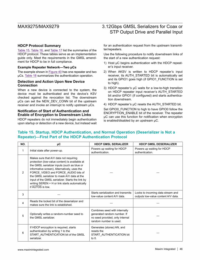
MAX9275/MAX9279 3.12Gbps GMSL Serializers for Coax or STP Output Drive and Parallel Input
www.maximintegrated.com Maxim Integrated 46
HDCP Protocol SummaryTable 15, Table 16, and Table 17 list the summaries of the HDCP protocol. These tables serve as an implementation guide only. Meet the requirements in the GMSL amend-ment for HDCP to be in full compliance.
Example Repeater Network—Two µCsThe example shown in Figure 40 has one repeater and two µCs. Table 18 summarizes the authentication operation.
Detection and Action Upon New Device ConnectionWhen a new device is connected to the system, the device must be authenticated and the device’s KSV checked against the revocation list. The downstream µCs can set the NEW_DEV_CONN bit of the upstream receiver and invoke an interrupt to notify upstream µCs.
Notification of Start of Authentication and Enable of Encryption to Downstream LinksHDCP repeaters do not immediately begin authentication upon startup or detection of a new device, but instead wait
for an authentication request from the upstream transmit-ter/repeaters.Use the following procedure to notify downstream links of the start of a new authentication request:1) Host µC begins authentication with the HDCP repeat-
er’s input receiver.2) When AKSV is written to HDCP repeater’s input
receiver, its AUTH_STARTED bit is automatically set and its GPIO1 goes high (if GPIO1_FUNCTION is set to high).
3) HDCP repeater’s µC waits for a low-to-high transition on HDCP repeater input receiver’s AUTH_STARTED bit and/or GPIO1 (if configured) and starts authentica-tion downstream.
4) HDCP repeater’s µC resets the AUTH_STARTED bit.Set GPIO0_FUNCTION to high to have GPIO0 follow the ENCRYPTION_ENABLE bit of the receiver. The repeater µC can use this function for notification when encryption is enabled/disabled by an upstream µC.
Table 15. Startup, HDCP Authentication, and Normal Operation (Deserializer is Not a Repeater)—First Part of the HDCP Authentication Protocol
NO. µC HDCP GMSL SERIALIZER HDCP GMSL DESERIALIZER
1 Initial state after power-up. Powers up waiting for HDCP authentication.
Powers up waiting for HDCP authentication.
2
Makes sure that A/V data not requiring protection (low-value content) is available at the GMSL serializer inputs (such as blue or informative screen). Alternatively, uses the FORCE_VIDEO and FORCE_AUDIO bits of the GMSL serializer to mask A/V data at the input of the GMSL serializer. Starts the link by writing SEREN = H or link starts automatically if AUTOS is low.
— —
3 — Starts serialization and transmits low-value content A/V data.
Locks to incoming data stream and outputs low-value content A/V data.
4 Reads the locked bit of the deserializer and makes sure the link is established. — —
5 Optionally writes a random-number seed to the GMSL serializer.
Combines seed with internally generated random number. If no seed provided, only internal random number is used.
—
6
If HDCP encryption is required, starts authentication by writing 1 to the START_AUTHENTICATION bit of the GMSL serializer.
Generates (stores) AN, and resets the START_AUTHENTICATION bit to 0.
—
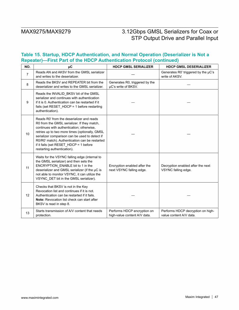
MAX9275/MAX9279 3.12Gbps GMSL Serializers for Coax or STP Output Drive and Parallel Input
www.maximintegrated.com Maxim Integrated 47
Table 15. Startup, HDCP Authentication, and Normal Operation (Deserializer is Not a Repeater)—First Part of the HDCP Authentication Protocol (continued)
NO. µC HDCP GMSL SERIALIZER HDCP GMSL DESERIALIZER
7 Reads AN and AKSV from the GMSL serializer and writes to the deserializer. — Generates R0’ triggered by the µC’s
write of AKSV.
8 Reads the BKSV and REPEATER bit from the deserializer and writes to the GMSL serializer.
Generates R0, triggered by the µC’s write of BKSV. —
9
Reads the INVALID_BKSV bit of the GMSL serializer and continues with authentication if it is 0. Authentication can be restarted if it fails (set RESET_HDCP = 1 before restarting authentication).
— —
10
Reads R0’ from the deserializer and reads R0 from the GMSL serializer. If they match, continues with authentication; otherwise, retries up to two more times (optionally, GMSL serializer comparison can be used to detect if R0/R0’ match). Authentication can be restarted if it fails (set RESET_HDCP = 1 before restarting authentication).
— —
11
Waits for the VSYNC falling edge (internal to the GMSL serializer) and then sets the ENCRYPTION_ENABLE bit to 1 in the deserializer and GMSL serializer (if the µC is not able to monitor VSYNC, it can utilize the VSYNC_DET bit in the GMSL serializer).
Encryption enabled after the next VSYNC falling edge.
Decryption enabled after the next VSYNC falling edge.
12
Checks that BKSV is not in the Key Revocation list and continues if it is not. Authentication can be restarted if it fails.Note: Revocation list check can start after BKSV is read in step 8.
— —
13 Starts transmission of A/V content that needs protection.
Performs HDCP encryption on high-value content A/V data.
Performs HDCP decryption on high-value content A/V data.
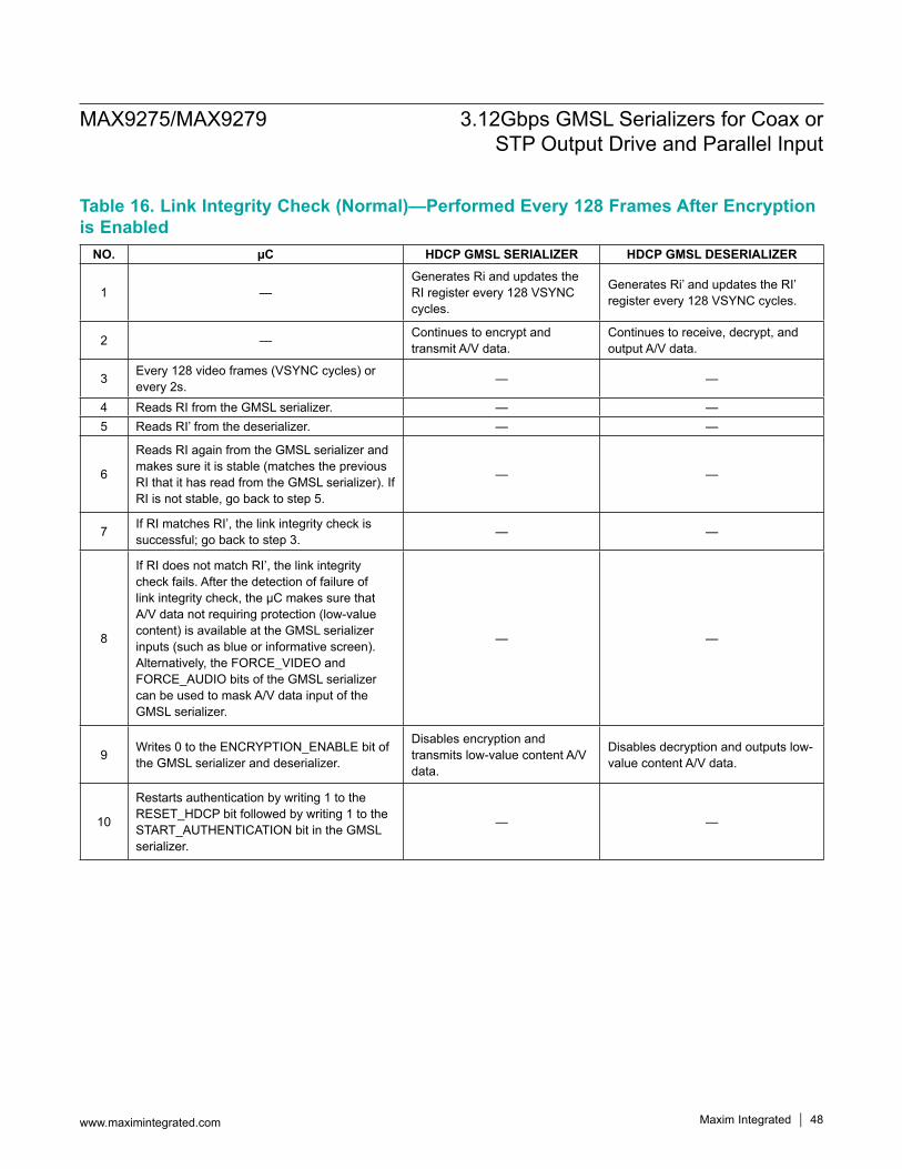
MAX9275/MAX9279 3.12Gbps GMSL Serializers for Coax or STP Output Drive and Parallel Input
www.maximintegrated.com Maxim Integrated 48
Table 16. Link Integrity Check (Normal)—Performed Every 128 Frames After Encryption is Enabled
NO. µC HDCP GMSL SERIALIZER HDCP GMSL DESERIALIZER
1 —Generates Ri and updates the RI register every 128 VSYNC cycles.
Generates Ri’ and updates the RI’ register every 128 VSYNC cycles.
2 — Continues to encrypt and transmit A/V data.
Continues to receive, decrypt, and output A/V data.
3 Every 128 video frames (VSYNC cycles) or every 2s. — —
4 Reads RI from the GMSL serializer. — —5 Reads RI’ from the deserializer. — —
6
Reads RI again from the GMSL serializer and makes sure it is stable (matches the previous RI that it has read from the GMSL serializer). If RI is not stable, go back to step 5.
— —
7 If RI matches RI’, the link integrity check is successful; go back to step 3. — —
8
If RI does not match RI’, the link integrity check fails. After the detection of failure of link integrity check, the µC makes sure that A/V data not requiring protection (low-value content) is available at the GMSL serializer inputs (such as blue or informative screen). Alternatively, the FORCE_VIDEO and FORCE_AUDIO bits of the GMSL serializer can be used to mask A/V data input of the GMSL serializer.
— —
9 Writes 0 to the ENCRYPTION_ENABLE bit of the GMSL serializer and deserializer.
Disables encryption and transmits low-value content A/V data.
Disables decryption and outputs low-value content A/V data.
10
Restarts authentication by writing 1 to the RESET_HDCP bit followed by writing 1 to the START_AUTHENTICATION bit in the GMSL serializer.
— —
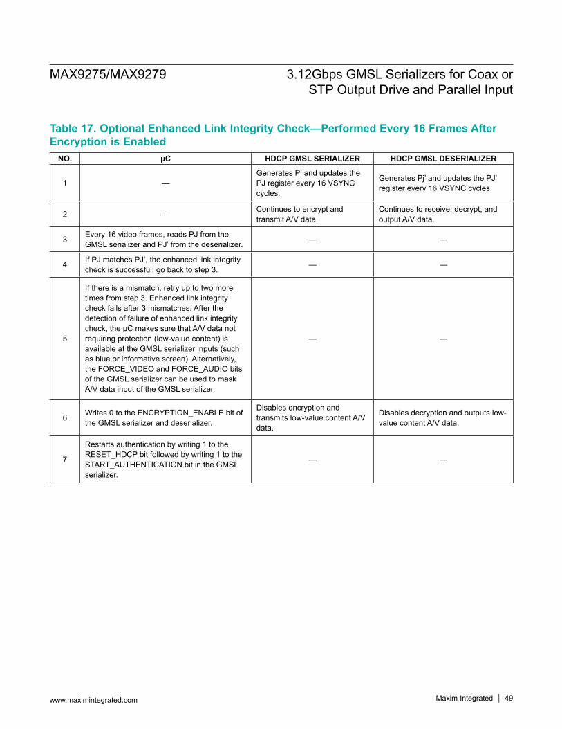
MAX9275/MAX9279 3.12Gbps GMSL Serializers for Coax or STP Output Drive and Parallel Input
www.maximintegrated.com Maxim Integrated 49
Table 17. Optional Enhanced Link Integrity Check—Performed Every 16 Frames After Encryption is Enabled
NO. µC HDCP GMSL SERIALIZER HDCP GMSL DESERIALIZER
1 —Generates Pj and updates the PJ register every 16 VSYNC cycles.
Generates Pj’ and updates the PJ’ register every 16 VSYNC cycles.
2 — Continues to encrypt and transmit A/V data.
Continues to receive, decrypt, and output A/V data.
3 Every 16 video frames, reads PJ from the GMSL serializer and PJ’ from the deserializer. — —
4 If PJ matches PJ’, the enhanced link integrity check is successful; go back to step 3. — —
5
If there is a mismatch, retry up to two more times from step 3. Enhanced link integrity check fails after 3 mismatches. After the detection of failure of enhanced link integrity check, the µC makes sure that A/V data not requiring protection (low-value content) is available at the GMSL serializer inputs (such as blue or informative screen). Alternatively, the FORCE_VIDEO and FORCE_AUDIO bits of the GMSL serializer can be used to mask A/V data input of the GMSL serializer.
— —
6 Writes 0 to the ENCRYPTION_ENABLE bit of the GMSL serializer and deserializer.
Disables encryption and transmits low-value content A/V data.
Disables decryption and outputs low-value content A/V data.
7
Restarts authentication by writing 1 to the RESET_HDCP bit followed by writing 1 to the START_AUTHENTICATION bit in the GMSL serializer.
— —
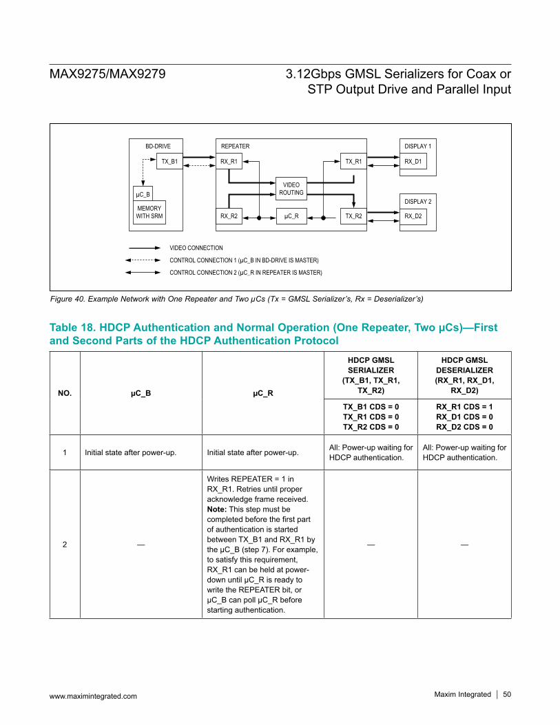
MAX9275/MAX9279 3.12Gbps GMSL Serializers for Coax or STP Output Drive and Parallel Input
www.maximintegrated.com Maxim Integrated 50
Table 18. HDCP Authentication and Normal Operation (One Repeater, Two µCs)—First and Second Parts of the HDCP Authentication Protocol
Figure 40. Example Network with One Repeater and Two µCs (Tx = GMSL Serializer’s, Rx = Deserializer’s)
BD-DRIVE
RX_R1
µC_B
TX_B1
DISPLAY 1
RX_D1
DISPLAY 2
RX_D2
REPEATER
TX_R1
TX_R2RX_R2 µC_R
VIDEOROUTING
MEMORYWITH SRM
VIDEO CONNECTION
CONTROL CONNECTION 1 (µC_B IN BD-DRIVE IS MASTER)
CONTROL CONNECTION 2 (µC_R IN REPEATER IS MASTER)
NO. µC_B µC_R
HDCP GMSL SERIALIZER
(TX_B1, TX_R1, TX_R2)
HDCP GMSL DESERIALIZER(RX_R1, RX_D1,
RX_D2)
TX_B1 CDS = 0TX_R1 CDS = 0TX_R2 CDS = 0
RX_R1 CDS = 1RX_D1 CDS = 0RX_D2 CDS = 0
1 Initial state after power-up. Initial state after power-up. All: Power-up waiting for HDCP authentication.
All: Power-up waiting for HDCP authentication.
2 —
Writes REPEATER = 1 in RX_R1. Retries until proper acknowledge frame received.Note: This step must be completed before the first part of authentication is started between TX_B1 and RX_R1 by the µC_B (step 7). For example, to satisfy this requirement, RX_R1 can be held at power-down until µC_R is ready to write the REPEATER bit, or µC_B can poll µC_R before starting authentication.
— —
MAX9275/MAX9279 3.12Gbps GMSL Serializers for Coax or STP Output Drive and Parallel Input
www.maximintegrated.com Maxim Integrated 51
Table 18. HDCP Authentication and Normal Operation (One Repeater, Two µCs)—First and Second Parts of the HDCP Authentication Protocol (continued)
NO. µC_B µC_R
HDCP GMSL SERIALIZER
(TX_B1, TX_R1, TX_R2)
HDCP GMSL DESERIALIZER(RX_R1, RX_D1,
RX_D2)
TX_B1 CDS = 0TX_R1 CDS = 0TX_R2 CDS = 0
RX_R1 CDS = 1RX_D1 CDS = 0RX_D2 CDS = 0
3
Makes sure that A/V data not requiring protection (low-value content) is available at the TX_B1 inputs (such as blue or informative screen). Alternatively, the FORCE_VIDEO and FORCE_AUDIO bits of TX_B1 can be used to mask A/V data input of TX_B1. Starts the link between TX_B1 and RX_R1 by writing SEREN = H to TX_B1, or link starts automatically if AUTOS is low.
—
TX_B1: Starts serialization and transmits low-value content A/V data.
RX_R1: Locks to incoming data stream and outputs low-value content A/V data.
4 —
Starts all downstream links by writing SEREN = H to TX_R1, TX_R2, or links start automatically if AUTOS of transmitters are low.
TX_R1, TX_R2: Starts serialization and transmits low-value content A/V data.
RX_D1, RX_D2: Locks to incoming data stream and outputs low-value content A/V data.
5
Reads the locked bit of RX_R1 and makes sure the link between TX_B1 and RX_R1 is established.
Reads the locked bit of RX_D1 and makes sure the link between TX_R1 and RX_D1 is established. Reads the locked bit of RX_D2 and makes sure the link between TX_R2 and RX_D2 is established.
— —
6 Optionally, writes a random number seed to TX_B1.
Writes 1 to the GPIO_0_FUNCTION and GPIO_1_FUNCTION bits in RX_R1 to change GPIO functionality used for HDCP purpose. Optionally, writes a random-number seed to TX_R1 and TX_R2.
— —
7
Starts and completes the first part of the authentication protocol between TX_B1, RX_R1 (see steps 6–10 in Table 15).
—
TX_B1: According to commands from µC_B, generates AN, computes R0.
RX_R1: According to commands from µC_B, computes R0’.
MAX9275/MAX9279 3.12Gbps GMSL Serializers for Coax or STP Output Drive and Parallel Input
www.maximintegrated.com Maxim Integrated 52
Table 18. HDCP Authentication and Normal Operation (One Repeater, Two µCs)—First and Second Parts of the HDCP Authentication Protocol (continued)
NO. µC_B µC_R
HDCP GMSL SERIALIZER
(TX_B1, TX_R1, TX_R2)
HDCP GMSL DESERIALIZER(RX_R1, RX_D1,
RX_D2)
TX_B1 CDS = 0TX_R1 CDS = 0TX_R2 CDS = 0
RX_R1 CDS = 1RX_D1 CDS = 0RX_D2 CDS = 0
8 —
When GPIO_1 = 1 is detected, starts and completes the first part of the authentication protocol between the (TX_R1, RX_D1) and (TX_R2, RX_D2) links (see steps 6–10 in Table 15.
TX_R1, TX_R2: According to commands from µC_R, generates AN, computes R0.
RX_D1, RX_D2: According to commands from µC_R, computes R0’.
9
Waits for the VSYNC falling edge and then enables encryption on the (TX_B1, RX_R1) link. Full authentication is not complete yet so it makes sure A/V content that needs protection is not transmitted. Since REPEATER = 1 was read from RX_R1, the second part of authentication is required.
—TX_B1: Encryption enabled after next VSYNC falling edge.
RX_R1: Decryption enabled after next VSYNC falling edge.
10 —
When GPIO_0 = 1 is detected, enables encryption on the (TX_R1, RX_D1) and (TX_R2, RX_D2) links.
TX_R1, TX_R2: Encryption enabled after next VSYNC falling edge.
RX_D1, RX_D2: Decryption enabled after next VSYNC falling edge.
11
Waits for some time to allow µC_R to make the KSV list ready in RX_R1. Then polls (reads) the KSV_LIST_READY bit of RX_R1 regularly until proper acknowledge frame is received and bit is read as 1.
Blocks control channel from µC_B side by setting REVCCEN = FWDCCEN = 0 in RX_R1. Retries until proper acknowledge frame received.
—
RX_R1: Control channel from serializer side (TX_B1) is blocked after FWDCCEN = REVCCEN = 0 is written.
12
Writes BKSVs of RX_D1 and RX_D2 to the KSV list in RX_R1. Then, calculates and writes the BINFO register of RX_R1.
—
RX_R1: Triggered by µC_R’s write of BINFO, calculates hash value (V’) on the KSV list, BINFO and the secret-value M0’.
13
Writes 1 to the KSV_LIST_READY bit of RX_R1 and then unblocks the control channel from the µC_B side by setting REVCCEN = FWDCCEN = 1 in RX_R1.
—
RX_R1: Control channel from the serializer side (TX_B1) is unblocked after FWDCCEN = REVCCEN = 1 is written.
MAX9275/MAX9279 3.12Gbps GMSL Serializers for Coax or STP Output Drive and Parallel Input
www.maximintegrated.com Maxim Integrated 53
Table 18. HDCP Authentication and Normal Operation (One Repeater, Two µCs)—First and Second Parts of the HDCP Authentication Protocol (continued)
NO. µC_B µC_R
HDCP GMSL SERIALIZER
(TX_B1, TX_R1, TX_R2)
HDCP GMSL DESERIALIZER(RX_R1, RX_D1,
RX_D2)
TX_B1 CDS = 0TX_R1 CDS = 0TX_R2 CDS = 0
RX_R1 CDS = 1RX_D1 CDS = 0RX_D2 CDS = 0
14
Reads the KSV list and BINFO from RX_R1 and writes them to TX_B1. If any of the MAX_DEVS_EXCEEDED or MAX_CASCADE_EXCEEDED bits is 1, then authentication fails. Note: BINFO must be written after the KSV list.
—
TX_B1: Triggered by µC_B’s write of BINFO, calculates hash value (V) on the KSV list, BINFO and the secret-value M0.
—
15
Reads V from TX_B1 and V’ from RX_R1. If they match, continues with authentication; otherwise, retries up to two more times.
— — —
16Searches for each KSV in the KSV list and BKSV of RX_R1 in the Key Revocation list.
— — —
17
If keys are not revoked, the second part of the authentication protocol is completed.
— — —
18 Starts transmission of A/V content that needs protection. —
All: Perform HDCP encryption on high-value A/V data.
All: Perform HDCP decryption on high-value A/V data.
MAX9275/MAX9279 3.12Gbps GMSL Serializers for Coax or STP Output Drive and Parallel Input
www.maximintegrated.com Maxim Integrated 54
Applications InformationSelf PRBS TestThe serializers include a PRBS pattern generator which works with bit-error verification in the deserializer. To run the PRBS test, disable encryption (if used), set DISHSFILT, DISVSFILT, and DISDEFILT to ‘1’, to disable glitch filter in the deserializer. Then, set PRBSEN = 1 (0x04, D5) in the serializer and then in the deserializer. To exit the PRBS test, set PRBSEN = 0 (0x04, D5) in the deserializer and then in the serializer.
Dual µC ControlUsually systems have one microcontroller to run the control channel, located on the serializer side for display applications or on the deserializer side for image-sensing applications. However, a µC can reside on each side simultaneously, and trade off running the control channel. In this case, each µC can communicate with the serializer and deserializer and any peripheral devices.Contention will occur if both µCs attempt to use the control channel at the same time. It is up to the user to prevent this contention by implementing a higher level protocol. In addition, the control channel does not provide arbitration between I2C masters on both sides of the link. An acknowledge frame is not generated when communication fails due to contention. If communication across the serial link is not required, the µCs can disable the forward and reverse control channel using the FWDCCEN and REVCCEN bits (0x04, D[1:0]) in the serializer/deserializer. Communication across the serial link is stopped and contention between µCs cannot occur.As an example of dual µC use in an image-sensing application, the serializer can be in sleep mode and waiting for wake-up by µC on the deserializer side. After wake-up, the serializer-side µC assumes master control of the serializer’s registers.Jitter-Filtering PLLIn some applications, the clock input (PCLKIN) includes noise, which reduces link reliability. The clock input has a programmable narrowband jitter-filter PLL that attenuates frequencies higher than 100kHz (typical). Enable the jitter-filter by setting DISJITFILT = 0 (0x05, D6).
PCLKIN Spread TrackingThe serializers can operate with a spread PCLKIN signal. When using a spread PCLKIN, disable the jitter-filter by setting DISJITFILT = 1 (0x05, D6). Do not exceed the spread limitation shown in Table 8. In addition, turn off
spread spectrum in the serializer and deserializer. The serializer and deserializer track the spread on PCLKIN.
Changing the Clock FrequencyIt is recommended that the serial link be enabled after the video clock (fPCLKIN) and the control-channel clock (fUART/fI2C) are stable. When changing the clock frequency, stop the video clock for 5µs, apply the clock at the new frequency, then restart the serial link or toggle SEREN. On-the-fly changes in clock frequency are possible if the new frequency is immediately stable and without glitches. The reverse control channel remains unavailable for 500μs after serial link start or stop. When using the UART interface, limit on-the-fly changes in fUART to factors of less than 3.5 at a time to ensure that the device recognizes the UART sync pattern. For example, when lowering the UART frequency from 1Mbps to 100kbps, first send data at 333kbps then at 100kbps for reduction ratios of 3 and 3.333, respectively.
Providing a Frame Sync (Camera Applications)The GPI/GPO provide a simple solution for camera applications that require a Frame Sync signal from the ECU (e.g., surround view systems). Connect the ECU Frame Sync signal to the GPI input, and connect GPO output to the camera Frame Sync input. GPI/GPO has a typical delay of 275µs. Skew between multiple GPI/GPO channels is typically 115µs. If a lower skew signal is required, connect the camera’s frame sync input one of the deserializer’s GPIOs and use an I2C broadcast write command to change the GPIO output state. This has a maximum skew of 0.5µs, + 1 I2C bit time.
Software Programming of the Device AddressesThe serializers and deserializers have programmable device addresses. This allows multiple GMSL devices, along with I2C peripherals, to coexist on the same control channel. The serializer device address is in register 0x00 of each device, while the deserializer device address is in register 0x01 of each device. To change a device address, first write to the device whose address changes (register 0x00 of the serializer for serializer device address change, or register 0x01 of the deserializer for deserializer device address change). Then write the same address into the corresponding register on the other device (register 0x00 of the deserializer for serializer device address change, or register 0x01 of the serializer for deserializer device address change).
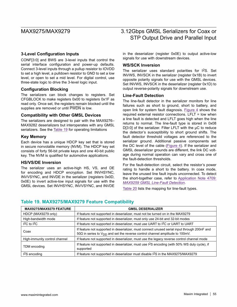
MAX9275/MAX9279 3.12Gbps GMSL Serializers for Coax or STP Output Drive and Parallel Input
www.maximintegrated.com Maxim Integrated 55
3-Level Configuration InputsCONF[3:0] and BWS are 3-level inputs that control the serial interface configuration and power-up defaults. Connect 3-level inputs through a pullup resistor to IOVDD to set a high level, a pulldown resistor to GND to set a low level, or open to set a mid level. For digital control, use three-state logic to drive the 3-level logic input.
Configuration BlockingThe serializers can block changes to registers. Set CFGBLOCK to make registers 0x00 to registers 0x1F as read only. Once set, the registers remain blocked until the supplies are removed or until PWDN is low.
Compatibility with Other GMSL DevicesThe serializers are designed to pair with the MAX9276–MAX9282 deserializers but interoperates with any GMSL serializers. See the Table 19 for operating limitations
Key MemoryEach device has a unique HDCP key set that is stored in secure nonvolatile memory (NVM). The HDCP key set consists of forty 56-bit private keys and one 40-bit public key. The NVM is qualified for automotive applications.
HS/VS/DE InversionThe serializer uses an active-high HS, VS, and DE for encoding and HDCP encryption. Set INVHSYNC, INVVSYNC, and INVDE in the serializer (registers 0x0D, 0x0E) to invert active-low input signals for use with the GMSL devices. Set INVHSYNC, INVVSYNC, and INVDE
in the deserializer (register 0x0E) to output active-low signals for use with downstream devices.
WS/SCK InversionThe serializer uses standard polarities for I2S. Set INVWS, INVSCK in the serializer (register 0x1B) to invert opposite polarity signals for use with the GMSL devices. Set INVWS, INVSCK in the deserializer (register 0x1D) to output reverse-polarity signals for downstream use.
Line-Fault DetectionThe line-fault detector in the serializer monitors for line failures such as short to ground, short to battery, and open link for system fault diagnosis. Figure 4 shows the required external resistor connections. LFLT = low when a line fault is detected and LFLT goes high when the line returns to normal. The line-fault type is stored in 0x08 D[3:0] of the serializer. Filter LFLT with the µC to reduce the detector’s susceptibility to short ground shifts. The fault detector threshold voltages are referenced to the serializer ground. Additional passive components set the DC level of the cable (Figure 4). If the serializer and GMSL deserializer grounds are different, the link DC volt-age during normal operation can vary and cross one of the fault-detection thresholds.For the fault-detection circuit, select the resistor’s power rating to handle a short to the battery. In coax mode, leave the unused line fault inputs unconnected. To detect the short-together case, refer to Application Note 4709: MAX9259 GMSL Line-Fault Detection.Table 20 lists the mapping for line-fault types.
Table 19. MAX9275/MAX9279 Feature CompatibilityMAX9275/MAX9279 FEATURE GMSL DESERIALIZER
HDCP (MAX9279 only) If feature not supported in deserializer, must not be turned on in the MAX9279High-bandwidth mode If feature not supported in deserializer, must only use 24-bit and 32-bit modesI2C to I2C If feature not supported in deserializer, must use UART to I2C or UART to UART
Coax If feature not supported in deserializer, must connect unused serial input through 200nF and 50Ω in series to VDD and set the reverse control channel amplitude to 100mV.
High-immunity control channel If feature not supported in deserializer, must use the legacy reverse control channel mode
TDM encoding If feature not supported in deserializer, must use I2S encoding (with 50% WS duty cycle), if supported
I2S encoding If feature not supported in deserializer must disable I2S in the MAX9275/MAX9279
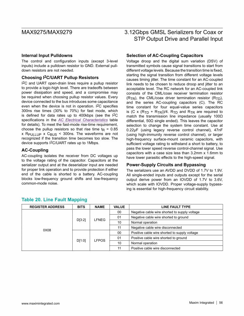
MAX9275/MAX9279 3.12Gbps GMSL Serializers for Coax or STP Output Drive and Parallel Input
www.maximintegrated.com Maxim Integrated 56
Internal Input PulldownsThe control and configuration inputs (except 3-level inputs) include a pulldown resistor to GND. External pull-down resistors are not needed.
Choosing I2C/UART Pullup ResistorsI2C and UART open-drain lines require a pullup resistor to provide a logic-high level. There are tradeoffs between power dissipation and speed, and a compromise may be required when choosing pullup resistor values. Every device connected to the bus introduces some capacitance even when the device is not in operation. I2C specifies 300ns rise times (30% to 70%) for fast mode, which is defined for data rates up to 400kbps (see the I2C specifications in the AC Electrical Characteristics table for details). To meet the fast-mode rise-time requirement, choose the pullup resistors so that rise time tR = 0.85 x RPULLUP x CBUS < 300ns. The waveforms are not recognized if the transition time becomes too slow. The device supports I2C/UART rates up to 1Mbps.
AC-CouplingAC-coupling isolates the receiver from DC voltages up to the voltage rating of the capacitor. Capacitors at the serializer output and at the deserializer input are needed for proper link operation and to provide protection if either end of the cable is shorted to a battery. AC-coupling blocks low-frequency ground shifts and low-frequency common-mode noise.
Selection of AC-Coupling CapacitorsVoltage droop and the digital sum variation (DSV) of transmitted symbols cause signal transitions to start from different voltage levels. Because the transition time is fixed, starting the signal transition from different voltage levels causes timing jitter. The time constant for an AC-coupled link needs to be chosen to reduce droop and jitter to an acceptable level. The RC network for an AC-coupled link consists of the CML/coax receiver termination resistor (RTR), the CML/coax driver termination resistor (RTD), and the series AC-coupling capacitors (C). The RC time constant for four equal-value series capacitors is (C x (RTD + RTR))/4. RTD and RTR are required to match the transmission line impedance (usually 100Ω differential, 50Ω single ended). This leaves the capacitor selection to change the system time constant. Use at 0.22µF (using legacy reverse control channel), 47nF (using high-immunity reverse control channel), or larger high-frequency surface-mount ceramic capacitors, with sufficient voltage rating to withstand a short to battery, to pass the lower speed reverse control-channel signal. Use capacitors with a case size less than 3.2mm x 1.6mm to have lower parasitic effects to the high-speed signal.
Power-Supply Circuits and BypassingThe serializers use an AVDD and DVDD of 1.7V to 1.9V. All single-ended inputs and outputs except for the serial output derive power from an IOVDD of 1.7V to 3.6V, which scale with IOVDD. Proper voltage-supply bypass-ing is essential for high-frequency circuit stability.
Table 20. Line Fault MappingREGISTER ADDRESS BITS NAME VALUE LINE FAULT TYPE
0X08
D[3:2] LFNEG
00 Negative cable wire shorted to supply voltage01 Negative cable wire shorted to ground10 Normal operation11 Negative cable wire disconnected
D[1:0] LFPOS
00 Positive cable wire shorted to supply voltage01 Positive cable wire shorted to ground10 Normal operation11 Positive cable wire disconnected
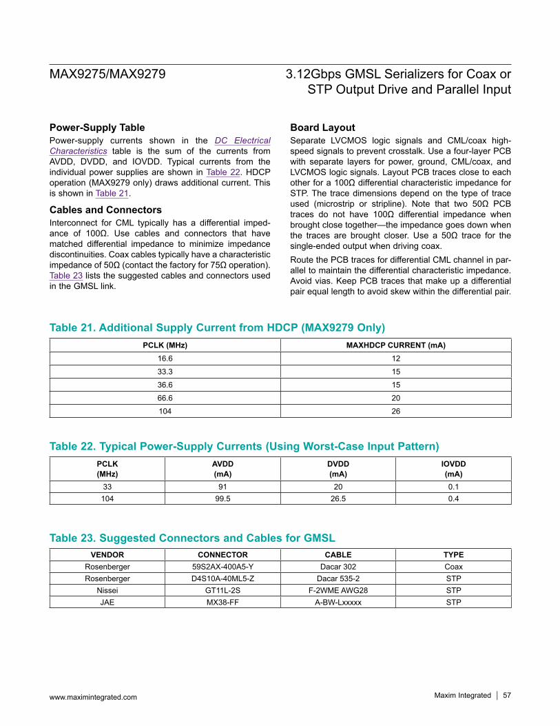
MAX9275/MAX9279 3.12Gbps GMSL Serializers for Coax or STP Output Drive and Parallel Input
www.maximintegrated.com Maxim Integrated 57
Power-Supply TablePower-supply currents shown in the DC Electrical Characteristics table is the sum of the currents from AVDD, DVDD, and IOVDD. Typical currents from the individual power supplies are shown in Table 22. HDCP operation (MAX9279 only) draws additional current. This is shown in Table 21.
Cables and ConnectorsInterconnect for CML typically has a differential imped-ance of 100Ω. Use cables and connectors that have matched differential impedance to minimize impedance discontinuities. Coax cables typically have a characteristic impedance of 50Ω (contact the factory for 75Ω operation). Table 23 lists the suggested cables and connectors used in the GMSL link.
Board LayoutSeparate LVCMOS logic signals and CML/coax high-speed signals to prevent crosstalk. Use a four-layer PCB with separate layers for power, ground, CML/coax, and LVCMOS logic signals. Layout PCB traces close to each other for a 100Ω differential characteristic impedance for STP. The trace dimensions depend on the type of trace used (microstrip or stripline). Note that two 50Ω PCB traces do not have 100Ω differential impedance when brought close together—the impedance goes down when the traces are brought closer. Use a 50Ω trace for the single-ended output when driving coax.Route the PCB traces for differential CML channel in par-allel to maintain the differential characteristic impedance. Avoid vias. Keep PCB traces that make up a differential pair equal length to avoid skew within the differential pair.
Table 23. Suggested Connectors and Cables for GMSL
Table 22. Typical Power-Supply Currents (Using Worst-Case Input Pattern)
Table 21. Additional Supply Current from HDCP (MAX9279 Only)
PCLK(MHz)
AVDD(mA)
DVDD(mA)
IOVDD(mA)
33 91 20 0.1104 99.5 26.5 0.4
VENDOR CONNECTOR CABLE TYPERosenberger 59S2AX-400A5-Y Dacar 302 CoaxRosenberger D4S10A-40ML5-Z Dacar 535-2 STP
Nissei GT11L-2S F-2WME AWG28 STPJAE MX38-FF A-BW-Lxxxxx STP
PCLK (MHz) MAXHDCP CURRENT (mA)16.6 1233.3 1536.6 1566.6 20104 26
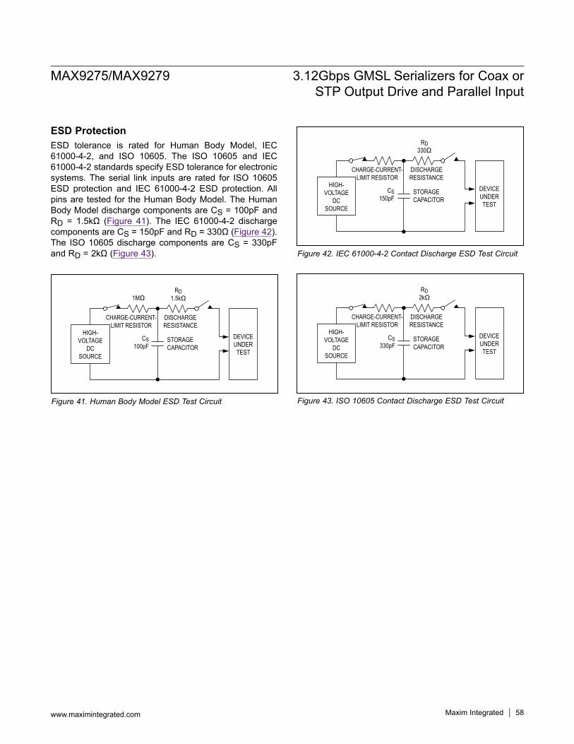
MAX9275/MAX9279 3.12Gbps GMSL Serializers for Coax or STP Output Drive and Parallel Input
www.maximintegrated.com Maxim Integrated 58
ESD ProtectionESD tolerance is rated for Human Body Model, IEC 61000-4-2, and ISO 10605. The ISO 10605 and IEC 61000-4-2 standards specify ESD tolerance for electronic systems. The serial link inputs are rated for ISO 10605 ESD protection and IEC 61000-4-2 ESD protection. All pins are tested for the Human Body Model. The Human Body Model discharge components are CS = 100pF and RD = 1.5kΩ (Figure 41). The IEC 61000-4-2 discharge components are CS = 150pF and RD = 330Ω (Figure 42). The ISO 10605 discharge components are CS = 330pF and RD = 2kΩ (Figure 43).
Figure 41. Human Body Model ESD Test Circuit
Figure 42. IEC 61000-4-2 Contact Discharge ESD Test Circuit
Figure 43. ISO 10605 Contact Discharge ESD Test Circuit
STORAGECAPACITOR
HIGH-VOLTAGE
DCSOURCE
DEVICEUNDERTEST
CHARGE-CURRENT-LIMIT RESISTOR
DISCHARGERESISTANCE
1MΩRD
1.5kΩ
CS100pF
CS150pF
STORAGECAPACITOR
HIGH-VOLTAGE
DCSOURCE
DEVICEUNDERTEST
CHARGE-CURRENT-LIMIT RESISTOR
DISCHARGERESISTANCE
RD330Ω
STORAGECAPACITOR
HIGH-VOLTAGE
DCSOURCE
DEVICEUNDERTEST
CHARGE-CURRENT-LIMIT RESISTOR
DISCHARGERESISTANCE
RD2kΩ
CS330pF
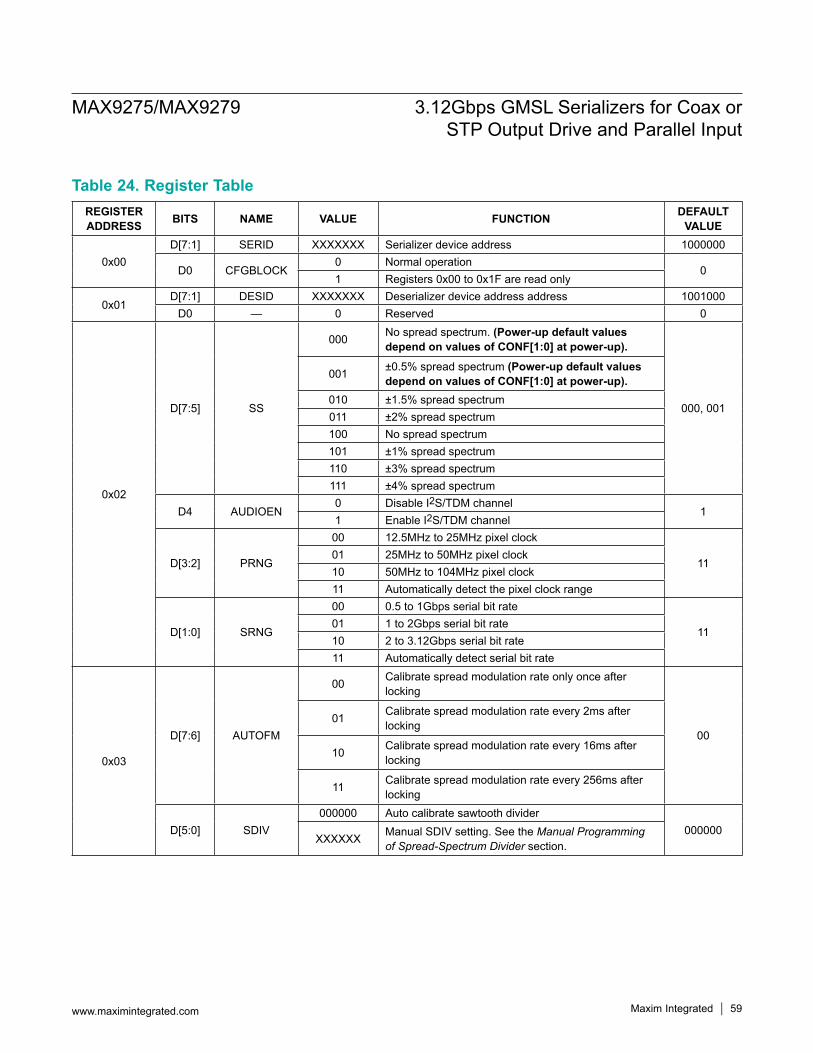
MAX9275/MAX9279 3.12Gbps GMSL Serializers for Coax or STP Output Drive and Parallel Input
www.maximintegrated.com Maxim Integrated 59
Table 24. Register TableREGISTER ADDRESS BITS NAME VALUE FUNCTION DEFAULT
VALUE
0x00D[7:1] SERID XXXXXXX Serializer device address 1000000
D0 CFGBLOCK0 Normal operation
01 Registers 0x00 to 0x1F are read only
0x01D[7:1] DESID XXXXXXX Deserializer device address address 1001000
D0 — 0 Reserved 0
0x02
D[7:5] SS
000 No spread spectrum. (Power-up default values depend on values of CONF[1:0] at power-up).
000, 001
001 ±0.5% spread spectrum (Power-up default values depend on values of CONF[1:0] at power-up).
010 ±1.5% spread spectrum011 ±2% spread spectrum100 No spread spectrum101 ±1% spread spectrum110 ±3% spread spectrum111 ±4% spread spectrum
D4 AUDIOEN0 Disable I2S/TDM channel
11 Enable I2S/TDM channel
D[3:2] PRNG
00 12.5MHz to 25MHz pixel clock
1101 25MHz to 50MHz pixel clock10 50MHz to 104MHz pixel clock11 Automatically detect the pixel clock range
D[1:0] SRNG
00 0.5 to 1Gbps serial bit rate
1101 1 to 2Gbps serial bit rate10 2 to 3.12Gbps serial bit rate11 Automatically detect serial bit rate
0x03
D[7:6] AUTOFM
00 Calibrate spread modulation rate only once after locking
0001 Calibrate spread modulation rate every 2ms after
locking
10 Calibrate spread modulation rate every 16ms after locking
11 Calibrate spread modulation rate every 256ms after locking
D[5:0] SDIV000000 Auto calibrate sawtooth divider
000000XXXXXX Manual SDIV setting. See the Manual Programming
of Spread-Spectrum Divider section.
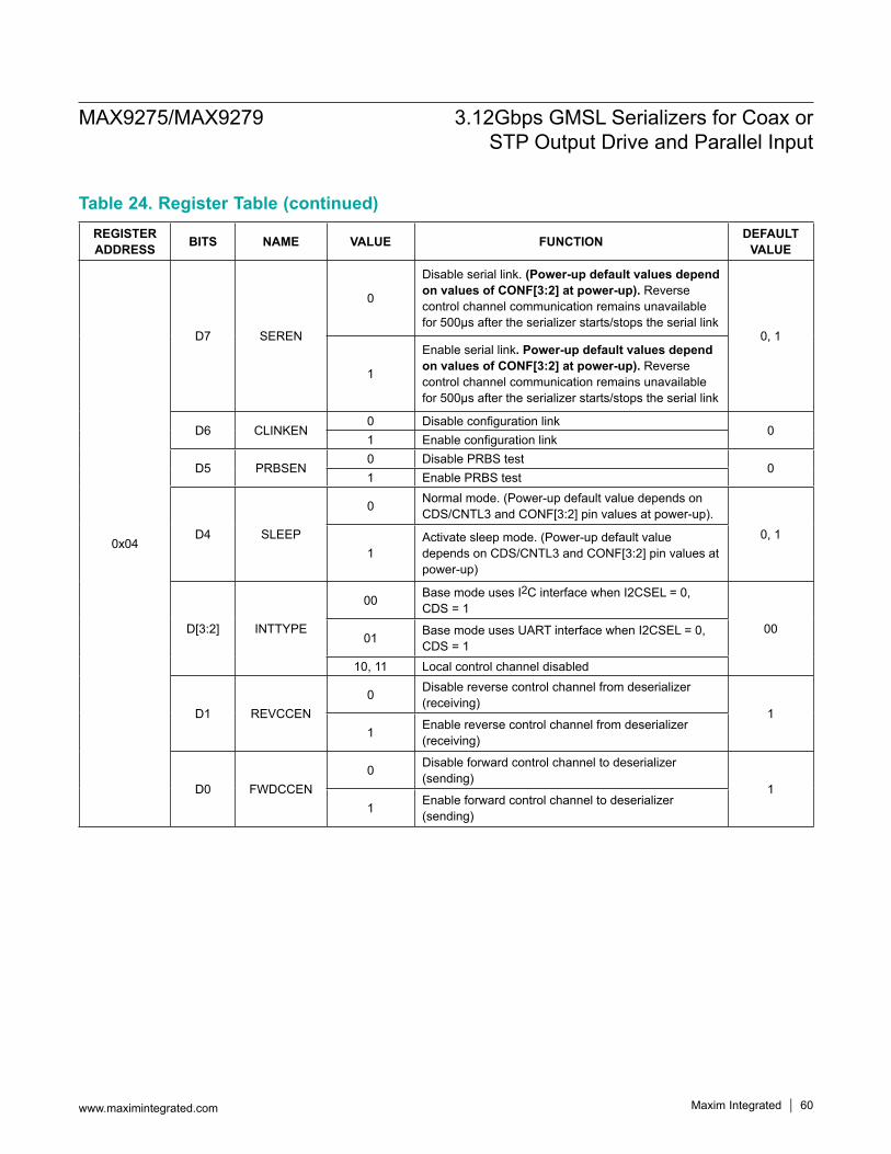
MAX9275/MAX9279 3.12Gbps GMSL Serializers for Coax or STP Output Drive and Parallel Input
www.maximintegrated.com Maxim Integrated 60
Table 24. Register Table (continued)REGISTER ADDRESS BITS NAME VALUE FUNCTION DEFAULT
VALUE
0x04
D7 SEREN
0
Disable serial link. (Power-up default values depend on values of CONF[3:2] at power-up). Reverse control channel communication remains unavailable for 500µs after the serializer starts/stops the serial link
0, 1
1
Enable serial link. Power-up default values depend on values of CONF[3:2] at power-up). Reverse control channel communication remains unavailable for 500µs after the serializer starts/stops the serial link
D6 CLINKEN0 Disable configuration link
01 Enable configuration link
D5 PRBSEN0 Disable PRBS test
01 Enable PRBS test
D4 SLEEP
0 Normal mode. (Power-up default value depends on CDS/CNTL3 and CONF[3:2] pin values at power-up).
0, 11
Activate sleep mode. (Power-up default value depends on CDS/CNTL3 and CONF[3:2] pin values at power-up)
D[3:2] INTTYPE
00 Base mode uses I2C interface when I2CSEL = 0, CDS = 1
0001 Base mode uses UART interface when I2CSEL = 0,
CDS = 110, 11 Local control channel disabled
D1 REVCCEN0 Disable reverse control channel from deserializer
(receiving)1
1 Enable reverse control channel from deserializer (receiving)
D0 FWDCCEN0 Disable forward control channel to deserializer
(sending)1
1 Enable forward control channel to deserializer (sending)
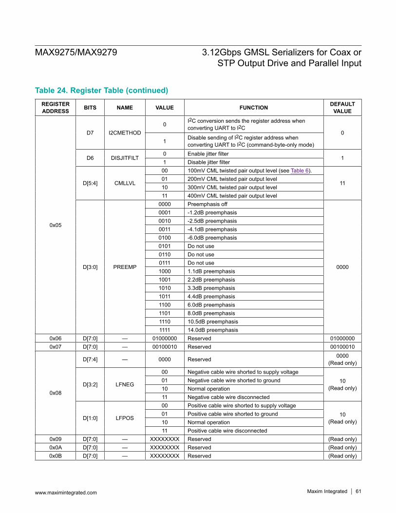
MAX9275/MAX9279 3.12Gbps GMSL Serializers for Coax or STP Output Drive and Parallel Input
www.maximintegrated.com Maxim Integrated 61
Table 24. Register Table (continued)REGISTER ADDRESS BITS NAME VALUE FUNCTION DEFAULT
VALUE
0x05
D7 I2CMETHOD0 I2C conversion sends the register address when
converting UART to I2C0
1 Disable sending of I2C register address when converting UART to I2C (command-byte-only mode)
D6 DISJITFILT0 Enable jitter filter
11 Disable jitter filter
D[5:4] CMLLVL
00 100mV CML twisted pair output level (see Table 6).
1101 200mV CML twisted pair output level10 300mV CML twisted pair output level11 400mV CML twisted pair output level
D[3:0] PREEMP
0000 Preemphasis off
0000
0001 -1.2dB preemphasis0010 -2.5dB preemphasis0011 -4.1dB preemphasis0100 -6.0dB preemphasis0101 Do not use0110 Do not use0111 Do not use1000 1.1dB preemphasis1001 2.2dB preemphasis1010 3.3dB preemphasis1011 4.4dB preemphasis1100 6.0dB preemphasis1101 8.0dB preemphasis1110 10.5dB preemphasis1111 14.0dB preemphasis
0x06 D[7:0] — 01000000 Reserved 010000000x07 D[7:0] — 00100010 Reserved 00100010
0x08
D[7:4] — 0000 Reserved 0000(Read only)
D[3:2] LFNEG
00 Negative cable wire shorted to supply voltage10
(Read only)01 Negative cable wire shorted to ground10 Normal operation11 Negative cable wire disconnected
D[1:0] LFPOS
00 Positive cable wire shorted to supply voltage10
(Read only)01 Positive cable wire shorted to ground10 Normal operation11 Positive cable wire disconnected
0x09 D[7:0] — XXXXXXXX Reserved (Read only)0x0A D[7:0] — XXXXXXXX Reserved (Read only)0x0B D[7:0] — XXXXXXXX Reserved (Read only)
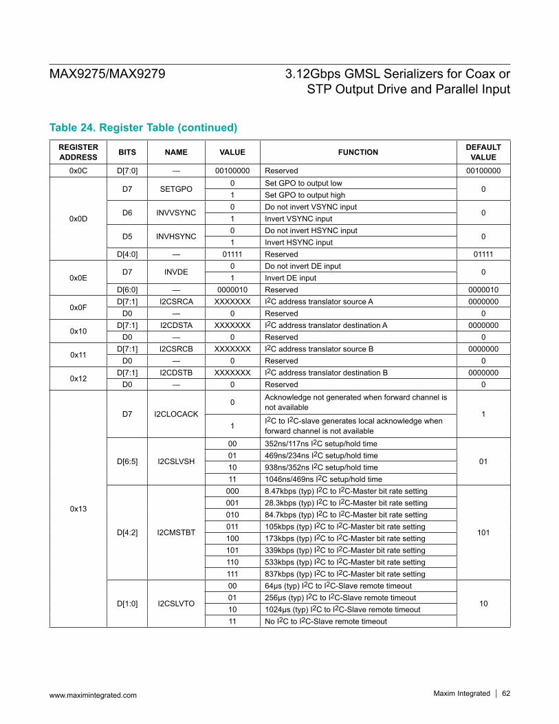
MAX9275/MAX9279 3.12Gbps GMSL Serializers for Coax or STP Output Drive and Parallel Input
www.maximintegrated.com Maxim Integrated 62
Table 24. Register Table (continued)REGISTER ADDRESS BITS NAME VALUE FUNCTION DEFAULT
VALUE0x0C D[7:0] — 00100000 Reserved 00100000
0x0D
D7 SETGPO0 Set GPO to output low
01 Set GPO to output high
D6 INVVSYNC0 Do not invert VSYNC input
01 Invert VSYNC input
D5 INVHSYNC0 Do not invert HSYNC input
01 Invert HSYNC input
D[4:0] — 01111 Reserved 01111
0x0ED7 INVDE
0 Do not invert DE input0
1 Invert DE inputD[6:0] — 0000010 Reserved 0000010
0x0FD[7:1] I2CSRCA XXXXXXX I2C address translator source A 0000000
D0 — 0 Reserved 0
0x10D[7:1] I2CDSTA XXXXXXX I2C address translator destination A 0000000
D0 — 0 Reserved 0
0x11D[7:1] I2CSRCB XXXXXXX I2C address translator source B 0000000
D0 — 0 Reserved 0
0x12D[7:1] I2CDSTB XXXXXXX I2C address translator destination B 0000000
D0 — 0 Reserved 0
0x13
D7 I2CLOCACK0 Acknowledge not generated when forward channel is
not available1
1 I2C to I2C-slave generates local acknowledge when forward channel is not available
D[6:5] I2CSLVSH
00 352ns/117ns I2C setup/hold time
0101 469ns/234ns I2C setup/hold time10 938ns/352ns I2C setup/hold time11 1046ns/469ns I2C setup/hold time
D[4:2] I2CMSTBT
000 8.47kbps (typ) I2C to I2C-Master bit rate setting
101
001 28.3kbps (typ) I2C to I2C-Master bit rate setting010 84.7kbps (typ) I2C to I2C-Master bit rate setting011 105kbps (typ) I2C to I2C-Master bit rate setting100 173kbps (typ) I2C to I2C-Master bit rate setting101 339kbps (typ) I2C to I2C-Master bit rate setting110 533kbps (typ) I2C to I2C-Master bit rate setting111 837kbps (typ) I2C to I2C-Master bit rate setting
D[1:0] I2CSLVTO
00 64µs (typ) I2C to I2C-Slave remote timeout
1001 256µs (typ) I2C to I2C-Slave remote timeout10 1024µs (typ) I2C to I2C-Slave remote timeout11 No I2C to I2C-Slave remote timeout
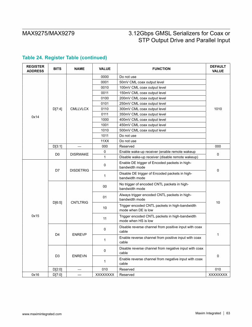
MAX9275/MAX9279 3.12Gbps GMSL Serializers for Coax or STP Output Drive and Parallel Input
www.maximintegrated.com Maxim Integrated 63
Table 24. Register Table (continued)REGISTER ADDRESS BITS NAME VALUE FUNCTION DEFAULT
VALUE
0x14
D[7:4] CMLLVLCX
0000 Do not use
1010
0001 50mV CML coax output level0010 100mV CML coax output level0011 150mV CML coax output level0100 200mV CML coax output level0101 250mV CML coax output level0110 300mV CML coax output level0111 350mV CML coax output level1000 400mV CML coax output level1001 450mV CML coax output level1010 500mV CML coax output level1011 Do not use11XX Do not use
D[3:1] — 000 Reserved 000
D0 DISRWAKE0 Enable wake-up receiver (enable remote wakeup
01 Disable wake-up receiver (disable remote wakeup)
0x15
D7 DISDETRIG0 Enable DE trigger of Encoded packets in high-
bandwidth mode0
1 Disable DE trigger of Encoded packets in high-bandwidth mode
D[6:5] CNTLTRIG
00 No trigger of encoded CNTL packets in high-bandwidth mode
1001 Always trigger encoded CNTL packets in high-
bandwidth mode
10 Trigger encoded CNTL packets in high-bandwidth mode when DE is low
11 Trigger encoded CNTL packets in high-bandwidth mode when HS is low
D4 ENREVP0 Disable reverse channel from positive input with coax
cable1
1 Enable reverse channel from positive input with coax cable
D3 ENREVN0 Disable reverse channel from negative input with coax
cable0
1 Enable reverse channel from negative input with coax cable
D[2:0] — 010 Reserved 0100x16 D[7:0] — XXXXXXXX Reserved XXXXXXXX
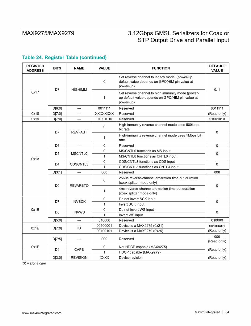
MAX9275/MAX9279 3.12Gbps GMSL Serializers for Coax or STP Output Drive and Parallel Input
www.maximintegrated.com Maxim Integrated 64
*X = Don’t care
Table 24. Register Table (continued)REGISTER ADDRESS BITS NAME VALUE FUNCTION DEFAULT
VALUE
0x17D7 HIGHIMM
0Set reverse channel to legacy mode. (power-up default value depends on GPO/HIM pin value at power-up)
0, 1
1Set reverse channel to high immunity mode (power-up default value depends on GPO/HIM pin value at power-up)
D[6:0] — 0011111 Reserved 00111110x18 D[7:0] — XXXXXXXX Reserved (Read only)0x19 D[7:0] — 01001010 Reserved 01001010
0x1A
D7 REVFAST0 High-immunity reverse channel mode uses 500kbps
bit rate0
1 High-immunity reverse channel mode uses 1Mbps bit rate
D6 — 0 Reserved 0
D5 MSCNTL00 MS/CNTL0 functions as MS input
01 MS/CNTL0 functions as CNTL0 input
D4 CDSCNTL30 CDS/CNTL3 functions as CDS input
01 CDS/CNTL3 functions as CNTL3 input
D[3:1] — 000 Reserved 000
D0 REVARBTO0 256µs reverse-channel arbitration time out duration
(coax splitter mode only)0
1 4ms reverse-channel arbitration time out duration (coax splitter mode only)
0x1B
D7 INVSCK0 Do not invert SCK input
01 Invert SCK input
D6 INVWS0 Do not invert WS input
01 Invert WS input
D[5:0] — 010000 Reserved 010000
0x1E D[7:0] ID00100001 Device is a MAX9275 (0x21) 00100X01
(Read only)00100101 Device is a MAX9279 (0x25)
0x1F
D[7:5] — 000 Reserved 000(Read only)
D4 CAPS0 Not HDCP capable (MAX9275)
(Read only)1 HDCP capable (MAX9279)
D[3:0] REVISION XXXX Device revision (Read only)
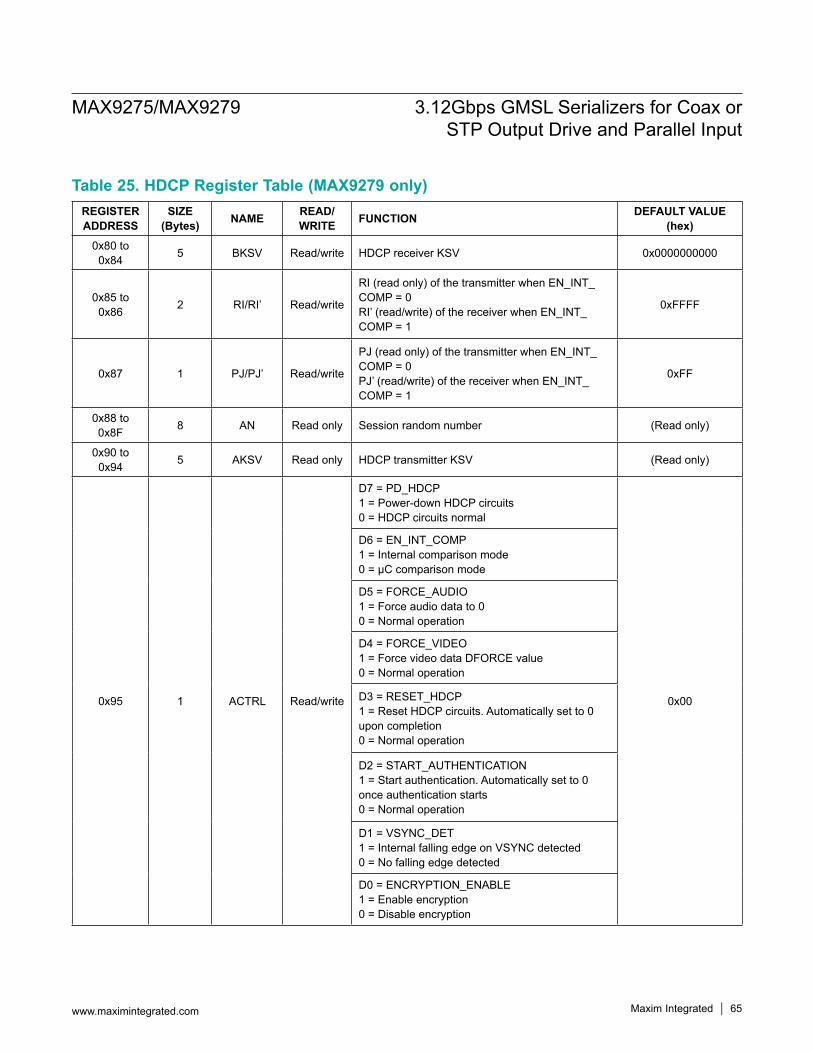
MAX9275/MAX9279 3.12Gbps GMSL Serializers for Coax or STP Output Drive and Parallel Input
www.maximintegrated.com Maxim Integrated 65
Table 25. HDCP Register Table (MAX9279 only)REGISTER ADDRESS
SIZE(Bytes) NAME READ/
WRITE FUNCTION DEFAULT VALUE(hex)
0x80 to 0x84 5 BKSV Read/write HDCP receiver KSV 0x0000000000
0x85 to 0x86 2 RI/RI’ Read/write
RI (read only) of the transmitter when EN_INT_COMP = 0RI’ (read/write) of the receiver when EN_INT_COMP = 1
0xFFFF
0x87 1 PJ/PJ’ Read/write
PJ (read only) of the transmitter when EN_INT_COMP = 0PJ’ (read/write) of the receiver when EN_INT_COMP = 1
0xFF
0x88 to 0x8F 8 AN Read only Session random number (Read only)
0x90 to 0x94 5 AKSV Read only HDCP transmitter KSV (Read only)
0x95 1 ACTRL Read/write
D7 = PD_HDCP1 = Power-down HDCP circuits0 = HDCP circuits normal
0x00
D6 = EN_INT_COMP1 = Internal comparison mode0 = µC comparison mode
D5 = FORCE_AUDIO1 = Force audio data to 00 = Normal operation
D4 = FORCE_VIDEO1 = Force video data DFORCE value0 = Normal operation
D3 = RESET_HDCP1 = Reset HDCP circuits. Automatically set to 0 upon completion0 = Normal operation
D2 = START_AUTHENTICATION1 = Start authentication. Automatically set to 0 once authentication starts0 = Normal operation
D1 = VSYNC_DET1 = Internal falling edge on VSYNC detected0 = No falling edge detected
D0 = ENCRYPTION_ENABLE1 = Enable encryption0 = Disable encryption
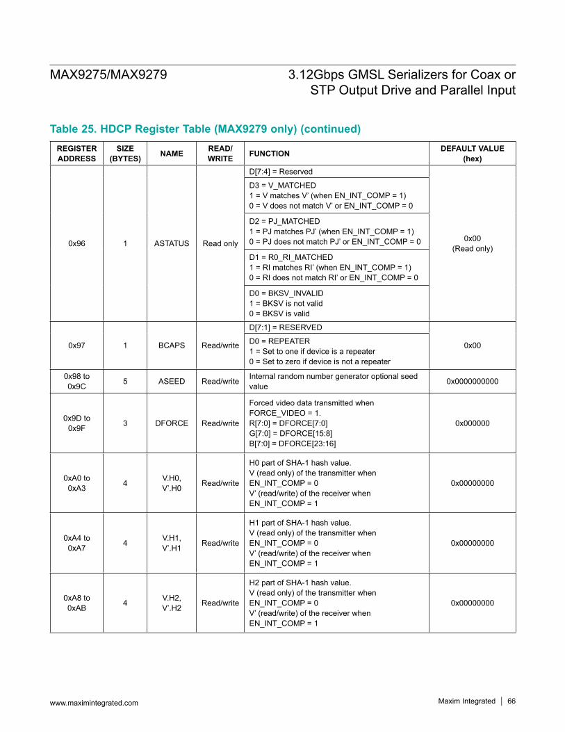
MAX9275/MAX9279 3.12Gbps GMSL Serializers for Coax or STP Output Drive and Parallel Input
www.maximintegrated.com Maxim Integrated 66
Table 25. HDCP Register Table (MAX9279 only) (continued)REGISTER ADDRESS
SIZE(BYTES) NAME READ/
WRITE FUNCTION DEFAULT VALUE(hex)
0x96 1 ASTATUS Read only
D[7:4] = Reserved
0x00(Read only)
D3 = V_MATCHED1 = V matches V’ (when EN_INT_COMP = 1)0 = V does not match V’ or EN_INT_COMP = 0
D2 = PJ_MATCHED1 = PJ matches PJ’ (when EN_INT_COMP = 1)0 = PJ does not match PJ’ or EN_INT_COMP = 0
D1 = R0_RI_MATCHED1 = RI matches RI’ (when EN_INT_COMP = 1)0 = RI does not match RI’ or EN_INT_COMP = 0
D0 = BKSV_INVALID1 = BKSV is not valid0 = BKSV is valid
0x97 1 BCAPS Read/write
D[7:1] = RESERVED
0x00D0 = REPEATER1 = Set to one if device is a repeater0 = Set to zero if device is not a repeater
0x98 to 0x9C 5 ASEED Read/write Internal random number generator optional seed
value 0x0000000000
0x9D to 0x9F 3 DFORCE Read/write
Forced video data transmitted when FORCE_VIDEO = 1.R[7:0] = DFORCE[7:0]G[7:0] = DFORCE[15:8]B[7:0] = DFORCE[23:16]
0x000000
0xA0 to 0xA3 4 V.H0,
V’.H0 Read/write
H0 part of SHA-1 hash value.V (read only) of the transmitter when EN_INT_COMP = 0V’ (read/write) of the receiver when EN_INT_COMP = 1
0x00000000
0xA4 to 0xA7 4 V.H1,
V’.H1 Read/write
H1 part of SHA-1 hash value.V (read only) of the transmitter when EN_INT_COMP = 0V’ (read/write) of the receiver when EN_INT_COMP = 1
0x00000000
0xA8 to 0xAB 4 V.H2,
V’.H2 Read/write
H2 part of SHA-1 hash value.V (read only) of the transmitter when EN_INT_COMP = 0V’ (read/write) of the receiver when EN_INT_COMP = 1
0x00000000
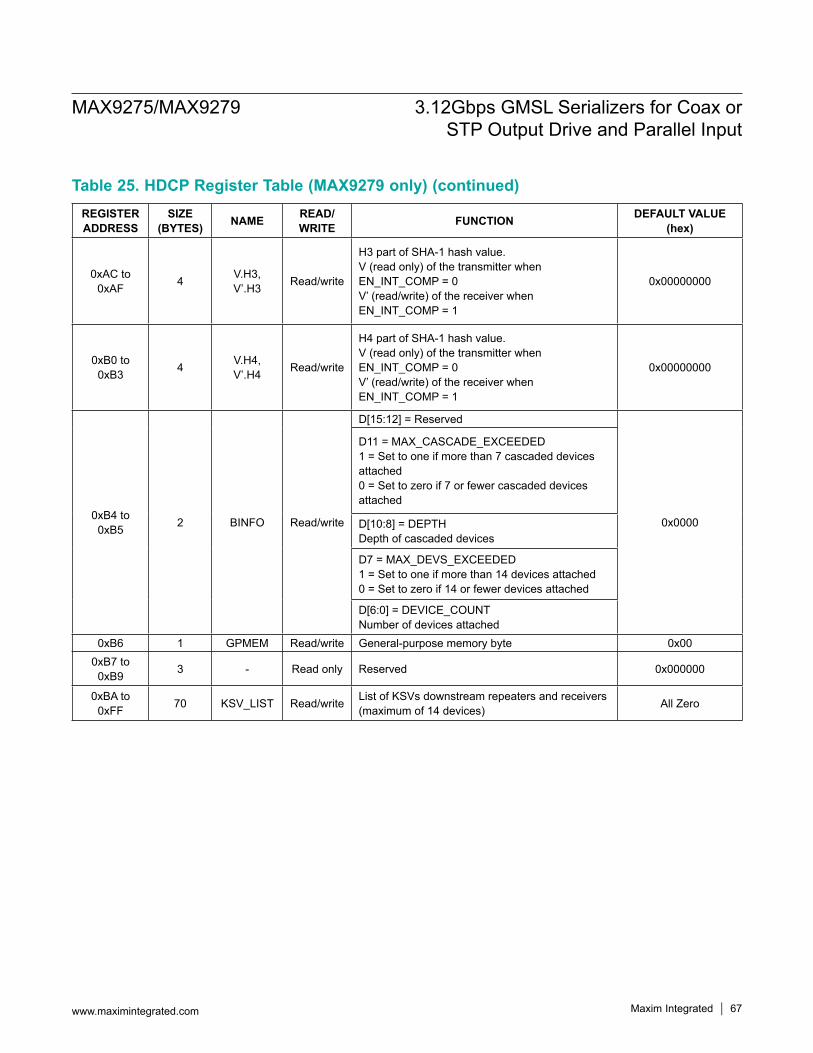
MAX9275/MAX9279 3.12Gbps GMSL Serializers for Coax or STP Output Drive and Parallel Input
www.maximintegrated.com Maxim Integrated 67
Table 25. HDCP Register Table (MAX9279 only) (continued)REGISTER ADDRESS
SIZE(BYTES) NAME READ/
WRITE FUNCTION DEFAULT VALUE(hex)
0xAC to 0xAF 4 V.H3,
V’.H3 Read/write
H3 part of SHA-1 hash value.V (read only) of the transmitter when EN_INT_COMP = 0V’ (read/write) of the receiver when EN_INT_COMP = 1
0x00000000
0xB0 to 0xB3 4 V.H4,
V’.H4 Read/write
H4 part of SHA-1 hash value.V (read only) of the transmitter when EN_INT_COMP = 0V’ (read/write) of the receiver when EN_INT_COMP = 1
0x00000000
0xB4 to 0xB5 2 BINFO Read/write
D[15:12] = Reserved
0x0000
D11 = MAX_CASCADE_EXCEEDED1 = Set to one if more than 7 cascaded devices attached0 = Set to zero if 7 or fewer cascaded devices attached
D[10:8] = DEPTHDepth of cascaded devices
D7 = MAX_DEVS_EXCEEDED1 = Set to one if more than 14 devices attached0 = Set to zero if 14 or fewer devices attached
D[6:0] = DEVICE_COUNTNumber of devices attached
0xB6 1 GPMEM Read/write General-purpose memory byte 0x000xB7 to 0xB9 3 - Read only Reserved 0x000000
0xBA to 0xFF 70 KSV_LIST Read/write List of KSVs downstream repeaters and receivers
(maximum of 14 devices) All Zero
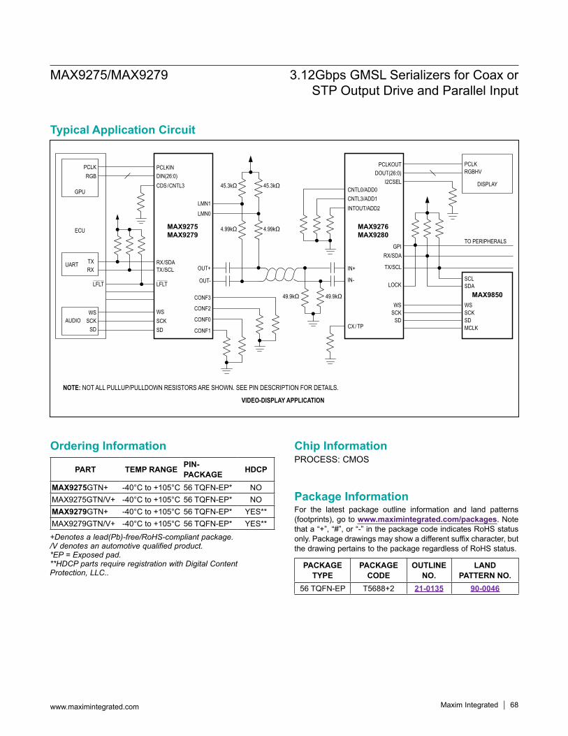
+Denotes a lead(Pb)-free/RoHS-compliant package. /V denotes an automotive qualified product. *EP = Exposed pad. **HDCP parts require registration with Digital Content Protection, LLC..
MAX9275/MAX9279 3.12Gbps GMSL Serializers for Coax or STP Output Drive and Parallel Input
www.maximintegrated.com Maxim Integrated 68
PACKAGE TYPE
PACKAGE CODE
OUTLINE NO.
LAND PATTERN NO.
56 TQFN-EP T5688+2 21-0135 90-0046
PCLKRGB
GPU
ECU
UART TXRX
AUDIOWS
SCKSD
PCLKINDIN(26:0)CDS /CNTL3
LMN0LMN1
OUT-
CONF3
CONF2
CONF0
CONF1
OUT+RX/SDATX/SCL
WS
SDSCK
SCLSDA
PCLKOUTDOUT(26:0)
I2CSEL
GPIRX/SDA
TX/SCL
LOCK
IN+
INTOUT/ADD2CNTL3/ADD1CNTL0/ADD0
IN-
CX / TP
WS
SDSCK
4.99kΩ4.99kΩ
45.3kΩ45.3kΩ
49.9kΩ49.9kΩWS
SDSCK
MCLK
PCLKRGBHV
TO PERIPHERALS
DISPLAY
MAX9850
MAX9276MAX9280
MAX9275MAX9279
NOTE: NOT ALL PULLUP/PULLDOWN RESISTORS ARE SHOWN. SEE PIN DESCRIPTION FOR DETAILS.
VIDEO-DISPLAY APPLICATION
LFLT LFLT
PART TEMP RANGE PIN-PACKAGE HDCP
MAX9275GTN+ -40°C to +105°C 56 TQFN-EP* NOMAX9275GTN/V+ -40°C to +105°C 56 TQFN-EP* NOMAX9279GTN+ -40°C to +105°C 56 TQFN-EP* YES**MAX9279GTN/V+ -40°C to +105°C 56 TQFN-EP* YES**
Typical Application Circuit
Ordering Information Chip InformationPROCESS: CMOS
Package InformationFor the latest package outline information and land patterns (footprints), go to www.maximintegrated.com/packages. Note that a “+”, “#”, or “-” in the package code indicates RoHS status only. Package drawings may show a different suffix character, but the drawing pertains to the package regardless of RoHS status.
Maxim Integrated cannot assume responsibility for use of any circuitry other than circuitry entirely embodied in a Maxim Integrated product. No circuit patent licenses are implied. Maxim Integrated reserves the right to change the circuitry and specifications without notice at any time. The parametric values (min and max limits) shown in the Electrical Characteristics table are guaranteed. Other parametric values quoted in this data sheet are provided for guidance.
Maxim Integrated and the Maxim Integrated logo are trademarks of Maxim Integrated Products, Inc.
MAX9275/MAX9279 3.12Gbps GMSL Serializers for Coax or STP Output Drive and Parallel Input
© 2017 Maxim Integrated Products, Inc. 69
REVISIONNUMBER
REVISIONDATE DESCRIPTION PAGES
CHANGED0 8/13 Initial release —1 7/15 Removed future product designations from Ordering Information 71
2 10/17 Fixed typos, clarified feature descriptions, removed old/unnecessary content (including Table 1)
2, 16–18, 20, 23, 25–29, 31, 33–36, 39, 40, 41–60, 62–71
3 12/17 Added a new Note 12 in the AC Electrical Characteristics table and renumbered the remaining three notes; replaced Figure 7 11, 12, 21
Revision History