Click here for production status of specific part …...or Coa or STP Inpt an MIPI CSI-2 Otpt Click...
103
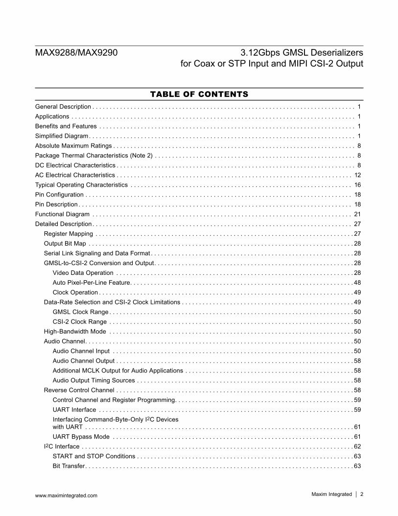
General Description The MAX9288/MAX9290 gigabit multimedia serial link (GMSL) deserializers receive data from a GMSL serializer over 50Ω coax or 100Ω shielded twisted-pair (STP) cable and output deserialized data on the CSI-2 outputs. The MAX9290 has HDCP content protection but other- wise is the same as the MAX9288. The deserializers pair with any GMSL serializer capable of coax output. When programmed for STP input, they are backward compatible with any GMSL serializer. The audio channel supports L-PCM I 2 S stereo and up to eight channels of L-PCM in TDM mode. Sample rates of 32kHz to 192kHz are supported with sample depth up to 32 bits. The embedded control channel operates at 9.6kbps to 1Mbps in UART-to-UART and UART-to-I 2 C modes, and up to 1Mbps in I 2 C-to-I 2 C mode. Using the control channel, a µC can program serializer, deserializer, and peripheral device registers at any time, independent of video timing, and manage HDCP operation (MAX9290). Two GPIO ports are included, allowing display power- up and switching of the backlight, among other uses. A continuously sampled GPI input supports touch-screen controller interrupt requests in display applications. For use with longer cables, the deserializers have a pro- grammable cable equalizer. The serial input meets ISO 10605 and IEC 61000-4-2 ESD standards. The GMSL supply is 3.0V to 3.6V, the MIPI CSI-2 supply is 1.7V to 1.9V, and the I/O supply is 1.7V to 3.6V. The devices are available in lead(Pb)-free, 48-pin, 7mm x 7mm TQFN and SWTQFN packages with exposed pad and 0.5mm lead pitch. Applications ● High-Resolution Automotive Navigation ● Rear-Seat Infotainment ● Megapixel Camera Systems Benefits and Features ● Ideal for High-Definition Video Applications • 4-Lane CSI-2 Output with Up to 1Gbps Per Lane • Works with Low-Cost 50Ω Coax Cable and FAKRA Connectors or 100Ω STP • 104MHz High-Bandwidth Mode Supports 1920 x 720p/60Hz Display with 24-Bit Color • Equalization Allows 15m Cable at Full Speed • Up to 192kHz Sample Rate and 32-Bit Sample Depth For 7.1 Channel HD Audio • Audio Clock from Audio Source or Audio Sink • Color Lookup Table for Gamma Correction • CNTL0–CNTL3 Control Outputs for HDMI/MHL ● Multiple Data Rates for System Flexibility • Up to 3.12Gbps Serial-Bit Rate • 6.25MHz to 104MHz Pixel Clock • 9.6kbps to 1Mbps Control Channel in UART, Mixed UART/I 2 C, or I 2 C Mode with Clock-Stretch Capability ● Reduces EMI and Shielding Requirements • Tracks Spread Spectrum on Input • High-Immunity Mode for Maximum Control- Channel Noise Rejection ● Peripheral Features for System Power-Up and Verification • Built-In PRBS Tester for BER Testing of the Serial Link • Programmable Choice of 8 Default Device Addresses • Two Dedicated GPIO Ports • Dedicated “Up/Down” GPI for Touch-Screen Interrupt and Other Uses • Remote/Local Wake-Up from Sleep Mode ● Meets Rigorous Automotive and Industrial Requirements • -40°C to +105°C Operating Temperature • ±8kV Contact and ±12kV Air ISO 10605 and IEC 61000-4-2 ESD Protection Ordering Information appears at end of data sheet. 19-6916; Rev 4; 3/18 MAX9288/MAX9290 3.12Gbps GMSL Deserializers for Coax or STP Input and MIPI CSI-2 Output Click here for production status of specific part numbers. Simplified Diagram µC GMSL SERIALIZER MAX9288 MAX9290 VIDEO/AUDIO I 2 C 720p DISPLAY CSI-2 VIDEO/ AUDIO I 2 C EVALUATION KIT AVAILABLE
Transcript of Click here for production status of specific part …...or Coa or STP Inpt an MIPI CSI-2 Otpt Click...
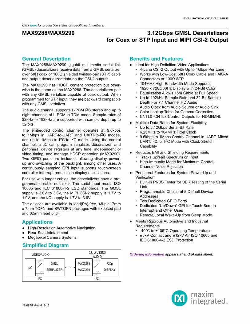
General DescriptionThe MAX9288/MAX9290 gigabit multimedia serial link (GMSL) deserializers receive data from a GMSL serializer over 50Ω coax or 100Ω shielded twisted-pair (STP) cable and output deserialized data on the CSI-2 outputs.The MAX9290 has HDCP content protection but other-wise is the same as the MAX9288. The deserializers pair with any GMSL serializer capable of coax output. When programmed for STP input, they are backward compatible with any GMSL serializer.The audio channel supports L-PCM I2S stereo and up to eight channels of L-PCM in TDM mode. Sample rates of 32kHz to 192kHz are supported with sample depth up to 32 bits.The embedded control channel operates at 9.6kbps to 1Mbps in UART-to-UART and UART-to-I2C modes, and up to 1Mbps in I2C-to-I2C mode. Using the control channel, a µC can program serializer, deserializer, and peripheral device registers at any time, independent of video timing, and manage HDCP operation (MAX9290). Two GPIO ports are included, allowing display power-up and switching of the backlight, among other uses. A continuously sampled GPI input supports touch-screen controller interrupt requests in display applications.For use with longer cables, the deserializers have a pro-grammable cable equalizer. The serial input meets ISO 10605 and IEC 61000-4-2 ESD standards. The GMSL supply is 3.0V to 3.6V, the MIPI CSI-2 supply is 1.7V to 1.9V, and the I/O supply is 1.7V to 3.6V.The devices are available in lead(Pb)-free, 48-pin, 7mm x 7mm TQFN and SWTQFN packages with exposed pad and 0.5mm lead pitch.
Applications High-Resolution Automotive Navigation Rear-Seat Infotainment Megapixel Camera Systems
Benefits and Features Ideal for High-Definition Video Applications
• 4-Lane CSI-2 Output with Up to 1Gbps Per Lane • Works with Low-Cost 50Ω Coax Cable and FAKRA Connectors or 100Ω STP • 104MHz High-Bandwidth Mode Supports 1920 x 720p/60Hz Display with 24-Bit Color • Equalization Allows 15m Cable at Full Speed • Up to 192kHz Sample Rate and 32-Bit Sample Depth For 7.1 Channel HD Audio • Audio Clock from Audio Source or Audio Sink • Color Lookup Table for Gamma Correction • CNTL0–CNTL3 Control Outputs for HDMI/MHL
Multiple Data Rates for System Flexibility • Up to 3.12Gbps Serial-Bit Rate • 6.25MHz to 104MHz Pixel Clock • 9.6kbps to 1Mbps Control Channel in UART, Mixed UART/I2C, or I2C Mode with Clock-Stretch Capability
Reduces EMI and Shielding Requirements • Tracks Spread Spectrum on Input • High-Immunity Mode for Maximum Control- Channel Noise Rejection
Peripheral Features for System Power-Up and Verification • Built-In PRBS Tester for BER Testing of the Serial Link • Programmable Choice of 8 Default Device Addresses • Two Dedicated GPIO Ports • Dedicated “Up/Down” GPI for Touch-Screen Interrupt and Other Uses • Remote/Local Wake-Up from Sleep Mode
Meets Rigorous Automotive and Industrial Requirements • -40°C to +105°C Operating Temperature • ±8kV Contact and ±12kV Air ISO 10605 and IEC 61000-4-2 ESD Protection
Ordering Information appears at end of data sheet.
19-6916; Rev 4; 3/18
MAX9288/MAX9290 3.12Gbps GMSL Deserializers for Coax or STP Input and MIPI CSI-2 Output
Click here for production status of specific part numbers.
Simplified Diagram
µCGMSL
SERIALIZER
MAX9288
MAX9290
VIDEO/AUDIO
I2C
720p
DISPLAY
CSI-2 VIDEO/AUDIO
I2C
EVALUATION KIT AVAILABLE
MAX9288/MAX9290 3.12Gbps GMSL Deserializers for Coax or STP Input and MIPI CSI-2 Output
www.maximintegrated.com Maxim Integrated 2
TABLE OF CONTENTSGeneral Description . . . . . . . . . . . . . . . . . . . . . . . . . . . . . . . . . . . . . . . . . . . . . . . . . . . . . . . . . . . . . . . . . . . . . . . . . . . . 1Applications . . . . . . . . . . . . . . . . . . . . . . . . . . . . . . . . . . . . . . . . . . . . . . . . . . . . . . . . . . . . . . . . . . . . . . . . . . . . . . . . . . 1Benefits and Features . . . . . . . . . . . . . . . . . . . . . . . . . . . . . . . . . . . . . . . . . . . . . . . . . . . . . . . . . . . . . . . . . . . . . . . . . . 1Simplified Diagram. . . . . . . . . . . . . . . . . . . . . . . . . . . . . . . . . . . . . . . . . . . . . . . . . . . . . . . . . . . . . . . . . . . . . . . . . . . . . 1Absolute Maximum Ratings . . . . . . . . . . . . . . . . . . . . . . . . . . . . . . . . . . . . . . . . . . . . . . . . . . . . . . . . . . . . . . . . . . . . . . 8Package Thermal Characteristics (Note 2) . . . . . . . . . . . . . . . . . . . . . . . . . . . . . . . . . . . . . . . . . . . . . . . . . . . . . . . . . . 8DC Electrical Characteristics . . . . . . . . . . . . . . . . . . . . . . . . . . . . . . . . . . . . . . . . . . . . . . . . . . . . . . . . . . . . . . . . . . . . . 8AC Electrical Characteristics . . . . . . . . . . . . . . . . . . . . . . . . . . . . . . . . . . . . . . . . . . . . . . . . . . . . . . . . . . . . . . . . . . . . 12Typical Operating Characteristics . . . . . . . . . . . . . . . . . . . . . . . . . . . . . . . . . . . . . . . . . . . . . . . . . . . . . . . . . . . . . . . . 16Pin Configuration . . . . . . . . . . . . . . . . . . . . . . . . . . . . . . . . . . . . . . . . . . . . . . . . . . . . . . . . . . . . . . . . . . . . . . . . . . . . . 18Pin Description . . . . . . . . . . . . . . . . . . . . . . . . . . . . . . . . . . . . . . . . . . . . . . . . . . . . . . . . . . . . . . . . . . . . . . . . . . . . . . . 18Functional Diagram . . . . . . . . . . . . . . . . . . . . . . . . . . . . . . . . . . . . . . . . . . . . . . . . . . . . . . . . . . . . . . . . . . . . . . . . . . . 21Detailed Description. . . . . . . . . . . . . . . . . . . . . . . . . . . . . . . . . . . . . . . . . . . . . . . . . . . . . . . . . . . . . . . . . . . . . . . . . . . 27
Register Mapping . . . . . . . . . . . . . . . . . . . . . . . . . . . . . . . . . . . . . . . . . . . . . . . . . . . . . . . . . . . . . . . . . . . . . . . . . . . 27Output Bit Map . . . . . . . . . . . . . . . . . . . . . . . . . . . . . . . . . . . . . . . . . . . . . . . . . . . . . . . . . . . . . . . . . . . . . . . . . . . . . 28Serial Link Signaling and Data Format . . . . . . . . . . . . . . . . . . . . . . . . . . . . . . . . . . . . . . . . . . . . . . . . . . . . . . . . . . . 28GMSL-to-CSI-2 Conversion and Output. . . . . . . . . . . . . . . . . . . . . . . . . . . . . . . . . . . . . . . . . . . . . . . . . . . . . . . . . . 28
Video Data Operation . . . . . . . . . . . . . . . . . . . . . . . . . . . . . . . . . . . . . . . . . . . . . . . . . . . . . . . . . . . . . . . . . . . . . 28Auto Pixel-Per-Line Feature. . . . . . . . . . . . . . . . . . . . . . . . . . . . . . . . . . . . . . . . . . . . . . . . . . . . . . . . . . . . . . . . . 48Clock Operation . . . . . . . . . . . . . . . . . . . . . . . . . . . . . . . . . . . . . . . . . . . . . . . . . . . . . . . . . . . . . . . . . . . . . . . . . . 49
Data-Rate Selection and CSI-2 Clock Limitations . . . . . . . . . . . . . . . . . . . . . . . . . . . . . . . . . . . . . . . . . . . . . . . . . . 49GMSL Clock Range . . . . . . . . . . . . . . . . . . . . . . . . . . . . . . . . . . . . . . . . . . . . . . . . . . . . . . . . . . . . . . . . . . . . . . . 50CSI-2 Clock Range . . . . . . . . . . . . . . . . . . . . . . . . . . . . . . . . . . . . . . . . . . . . . . . . . . . . . . . . . . . . . . . . . . . . . . . 50
High-Bandwidth Mode . . . . . . . . . . . . . . . . . . . . . . . . . . . . . . . . . . . . . . . . . . . . . . . . . . . . . . . . . . . . . . . . . . . . . . . 50Audio Channel. . . . . . . . . . . . . . . . . . . . . . . . . . . . . . . . . . . . . . . . . . . . . . . . . . . . . . . . . . . . . . . . . . . . . . . . . . . . . . 50
Audio Channel Input . . . . . . . . . . . . . . . . . . . . . . . . . . . . . . . . . . . . . . . . . . . . . . . . . . . . . . . . . . . . . . . . . . . . . . 50Audio Channel Output . . . . . . . . . . . . . . . . . . . . . . . . . . . . . . . . . . . . . . . . . . . . . . . . . . . . . . . . . . . . . . . . . . . . . 58Additional MCLK Output for Audio Applications . . . . . . . . . . . . . . . . . . . . . . . . . . . . . . . . . . . . . . . . . . . . . . . . . 58Audio Output Timing Sources . . . . . . . . . . . . . . . . . . . . . . . . . . . . . . . . . . . . . . . . . . . . . . . . . . . . . . . . . . . . . . . 58
Reverse Control Channel . . . . . . . . . . . . . . . . . . . . . . . . . . . . . . . . . . . . . . . . . . . . . . . . . . . . . . . . . . . . . . . . . . . . . 58Control Channel and Register Programming. . . . . . . . . . . . . . . . . . . . . . . . . . . . . . . . . . . . . . . . . . . . . . . . . . . . 59UART Interface . . . . . . . . . . . . . . . . . . . . . . . . . . . . . . . . . . . . . . . . . . . . . . . . . . . . . . . . . . . . . . . . . . . . . . . . . . 59Interfacing Command-Byte-Only I2C Devices with UART . . . . . . . . . . . . . . . . . . . . . . . . . . . . . . . . . . . . . . . . . . . . . . . . . . . . . . . . . . . . . . . . . . . . . . . . . . . . . . 61UART Bypass Mode . . . . . . . . . . . . . . . . . . . . . . . . . . . . . . . . . . . . . . . . . . . . . . . . . . . . . . . . . . . . . . . . . . . . . . 61
I2C Interface . . . . . . . . . . . . . . . . . . . . . . . . . . . . . . . . . . . . . . . . . . . . . . . . . . . . . . . . . . . . . . . . . . . . . . . . . . . . . . . 62START and STOP Conditions . . . . . . . . . . . . . . . . . . . . . . . . . . . . . . . . . . . . . . . . . . . . . . . . . . . . . . . . . . . . . . . 63Bit Transfer. . . . . . . . . . . . . . . . . . . . . . . . . . . . . . . . . . . . . . . . . . . . . . . . . . . . . . . . . . . . . . . . . . . . . . . . . . . . . . 63
MAX9288/MAX9290 3.12Gbps GMSL Deserializers for Coax or STP Input and MIPI CSI-2 Output
www.maximintegrated.com Maxim Integrated 3
TABLE OF CONTENTS (continued)Acknowledge . . . . . . . . . . . . . . . . . . . . . . . . . . . . . . . . . . . . . . . . . . . . . . . . . . . . . . . . . . . . . . . . . . . . . . . . . . . . 63Slave Address . . . . . . . . . . . . . . . . . . . . . . . . . . . . . . . . . . . . . . . . . . . . . . . . . . . . . . . . . . . . . . . . . . . . . . . . . . . 64Bus Reset. . . . . . . . . . . . . . . . . . . . . . . . . . . . . . . . . . . . . . . . . . . . . . . . . . . . . . . . . . . . . . . . . . . . . . . . . . . . . . . 65Format for Reading . . . . . . . . . . . . . . . . . . . . . . . . . . . . . . . . . . . . . . . . . . . . . . . . . . . . . . . . . . . . . . . . . . . . . . . 66I2C Communication with Remote-Side Devices . . . . . . . . . . . . . . . . . . . . . . . . . . . . . . . . . . . . . . . . . . . . . . . . . 66
I2C Address Translation . . . . . . . . . . . . . . . . . . . . . . . . . . . . . . . . . . . . . . . . . . . . . . . . . . . . . . . . . . . . . . . . . . . . . . 67GPO/GPI Control . . . . . . . . . . . . . . . . . . . . . . . . . . . . . . . . . . . . . . . . . . . . . . . . . . . . . . . . . . . . . . . . . . . . . . . . . . . 67Line Equalizer . . . . . . . . . . . . . . . . . . . . . . . . . . . . . . . . . . . . . . . . . . . . . . . . . . . . . . . . . . . . . . . . . . . . . . . . . . . . . . 67HS/VS/DE Tracking. . . . . . . . . . . . . . . . . . . . . . . . . . . . . . . . . . . . . . . . . . . . . . . . . . . . . . . . . . . . . . . . . . . . . . . . . . 67Serial Input . . . . . . . . . . . . . . . . . . . . . . . . . . . . . . . . . . . . . . . . . . . . . . . . . . . . . . . . . . . . . . . . . . . . . . . . . . . . . . . . 67Coax Splitter Mode . . . . . . . . . . . . . . . . . . . . . . . . . . . . . . . . . . . . . . . . . . . . . . . . . . . . . . . . . . . . . . . . . . . . . . . . . . 68Cable Type Configuration Input . . . . . . . . . . . . . . . . . . . . . . . . . . . . . . . . . . . . . . . . . . . . . . . . . . . . . . . . . . . . . . . . 69Color Lookup Tables . . . . . . . . . . . . . . . . . . . . . . . . . . . . . . . . . . . . . . . . . . . . . . . . . . . . . . . . . . . . . . . . . . . . . . . . . 69
Programming and Verifying LUT Data. . . . . . . . . . . . . . . . . . . . . . . . . . . . . . . . . . . . . . . . . . . . . . . . . . . . . . . . . 69LUT Color Translation . . . . . . . . . . . . . . . . . . . . . . . . . . . . . . . . . . . . . . . . . . . . . . . . . . . . . . . . . . . . . . . . . . . . . 69LUT Bit Width. . . . . . . . . . . . . . . . . . . . . . . . . . . . . . . . . . . . . . . . . . . . . . . . . . . . . . . . . . . . . . . . . . . . . . . . . . . . 70Recommended LUT Program Procedure . . . . . . . . . . . . . . . . . . . . . . . . . . . . . . . . . . . . . . . . . . . . . . . . . . . . . . 70
High-Immunity Reverse Control-Channel Mode. . . . . . . . . . . . . . . . . . . . . . . . . . . . . . . . . . . . . . . . . . . . . . . . . . . . 71Sleep Mode . . . . . . . . . . . . . . . . . . . . . . . . . . . . . . . . . . . . . . . . . . . . . . . . . . . . . . . . . . . . . . . . . . . . . . . . . . . . . . . . 71Power-Down Mode . . . . . . . . . . . . . . . . . . . . . . . . . . . . . . . . . . . . . . . . . . . . . . . . . . . . . . . . . . . . . . . . . . . . . . . . . . 71Configuration Link . . . . . . . . . . . . . . . . . . . . . . . . . . . . . . . . . . . . . . . . . . . . . . . . . . . . . . . . . . . . . . . . . . . . . . . . . . . 72Link Startup Procedure . . . . . . . . . . . . . . . . . . . . . . . . . . . . . . . . . . . . . . . . . . . . . . . . . . . . . . . . . . . . . . . . . . . . . . . 72
High-Bandwidth Digital Content Protection (HDCP) . . . . . . . . . . . . . . . . . . . . . . . . . . . . . . . . . . . . . . . . . . . . . . . . . . 73Encryption Enable. . . . . . . . . . . . . . . . . . . . . . . . . . . . . . . . . . . . . . . . . . . . . . . . . . . . . . . . . . . . . . . . . . . . . . . . . . . 73Synchronization of Encryption . . . . . . . . . . . . . . . . . . . . . . . . . . . . . . . . . . . . . . . . . . . . . . . . . . . . . . . . . . . . . . . . . 73Repeater Support . . . . . . . . . . . . . . . . . . . . . . . . . . . . . . . . . . . . . . . . . . . . . . . . . . . . . . . . . . . . . . . . . . . . . . . . . . . 73
HDCP Authentication Procedures . . . . . . . . . . . . . . . . . . . . . . . . . . . . . . . . . . . . . . . . . . . . . . . . . . . . . . . . . . . . . . . . .74HDCP Protocol Summary . . . . . . . . . . . . . . . . . . . . . . . . . . . . . . . . . . . . . . . . . . . . . . . . . . . . . . . . . . . . . . . . . . . . . 74
Example Repeater Network—Two µCs . . . . . . . . . . . . . . . . . . . . . . . . . . . . . . . . . . . . . . . . . . . . . . . . . . . . . . . . 78Detection and Action Upon New Device Connection . . . . . . . . . . . . . . . . . . . . . . . . . . . . . . . . . . . . . . . . . . . . . . . . 78Notification of Start of Authentication and Enable of Encryption to Downstream Links . . . . . . . . . . . . . . . . . . . . . 82
Applications Information. . . . . . . . . . . . . . . . . . . . . . . . . . . . . . . . . . . . . . . . . . . . . . . . . . . . . . . . . . . . . . . . . . . . . . . . 82Self PRBS Test . . . . . . . . . . . . . . . . . . . . . . . . . . . . . . . . . . . . . . . . . . . . . . . . . . . . . . . . . . . . . . . . . . . . . . . . . . . . . 82Error Checking . . . . . . . . . . . . . . . . . . . . . . . . . . . . . . . . . . . . . . . . . . . . . . . . . . . . . . . . . . . . . . . . . . . . . . . . . . . . . 82ERR Output. . . . . . . . . . . . . . . . . . . . . . . . . . . . . . . . . . . . . . . . . . . . . . . . . . . . . . . . . . . . . . . . . . . . . . . . . . . . . . . . 82Auto Error Reset . . . . . . . . . . . . . . . . . . . . . . . . . . . . . . . . . . . . . . . . . . . . . . . . . . . . . . . . . . . . . . . . . . . . . . . . . . . . 83Dual µC Control . . . . . . . . . . . . . . . . . . . . . . . . . . . . . . . . . . . . . . . . . . . . . . . . . . . . . . . . . . . . . . . . . . . . . . . . . . . . 83Changing the Clock Frequency. . . . . . . . . . . . . . . . . . . . . . . . . . . . . . . . . . . . . . . . . . . . . . . . . . . . . . . . . . . . . . . . . 83
MAX9288/MAX9290 3.12Gbps GMSL Deserializers for Coax or STP Input and MIPI CSI-2 Output
www.maximintegrated.com Maxim Integrated 4
TABLE OF CONTENTS (continued)
Spread-Spectrum Clock Tracking. . . . . . . . . . . . . . . . . . . . . . . . . . . . . . . . . . . . . . . . . . . . . . . . . . . . . . . . . . . . . . . 83Fast Detection of Loss-of-Synchronization. . . . . . . . . . . . . . . . . . . . . . . . . . . . . . . . . . . . . . . . . . . . . . . . . . . . . . . . 83Providing a Frame Sync (Camera Applications). . . . . . . . . . . . . . . . . . . . . . . . . . . . . . . . . . . . . . . . . . . . . . . . . . . . 83Software Programming of the Device Addresses. . . . . . . . . . . . . . . . . . . . . . . . . . . . . . . . . . . . . . . . . . . . . . . . . . . 83Three-Level Configuration Inputs . . . . . . . . . . . . . . . . . . . . . . . . . . . . . . . . . . . . . . . . . . . . . . . . . . . . . . . . . . . . . . . 84Configuration Blocking . . . . . . . . . . . . . . . . . . . . . . . . . . . . . . . . . . . . . . . . . . . . . . . . . . . . . . . . . . . . . . . . . . . . . . . 84Compatibility with Other GMSL Devices . . . . . . . . . . . . . . . . . . . . . . . . . . . . . . . . . . . . . . . . . . . . . . . . . . . . . . . . . 84Key Memory . . . . . . . . . . . . . . . . . . . . . . . . . . . . . . . . . . . . . . . . . . . . . . . . . . . . . . . . . . . . . . . . . . . . . . . . . . . . . . . 84HS/VS/DE Inversion . . . . . . . . . . . . . . . . . . . . . . . . . . . . . . . . . . . . . . . . . . . . . . . . . . . . . . . . . . . . . . . . . . . . . . . . . 84WS/SCK Inversion . . . . . . . . . . . . . . . . . . . . . . . . . . . . . . . . . . . . . . . . . . . . . . . . . . . . . . . . . . . . . . . . . . . . . . . . . . 84GPIOs . . . . . . . . . . . . . . . . . . . . . . . . . . . . . . . . . . . . . . . . . . . . . . . . . . . . . . . . . . . . . . . . . . . . . . . . . . . . . . . . . . . . 84Line-Fault Detection . . . . . . . . . . . . . . . . . . . . . . . . . . . . . . . . . . . . . . . . . . . . . . . . . . . . . . . . . . . . . . . . . . . . . . . . . 84Internal Input Pulldowns . . . . . . . . . . . . . . . . . . . . . . . . . . . . . . . . . . . . . . . . . . . . . . . . . . . . . . . . . . . . . . . . . . . . . . 85Choosing I2C/UART Pullup Resistors. . . . . . . . . . . . . . . . . . . . . . . . . . . . . . . . . . . . . . . . . . . . . . . . . . . . . . . . . . . . 85AC-Coupling . . . . . . . . . . . . . . . . . . . . . . . . . . . . . . . . . . . . . . . . . . . . . . . . . . . . . . . . . . . . . . . . . . . . . . . . . . . . . . . 85Selection of AC-Coupling Capacitors . . . . . . . . . . . . . . . . . . . . . . . . . . . . . . . . . . . . . . . . . . . . . . . . . . . . . . . . . . . . 85Power-Supply Circuits and Bypassing . . . . . . . . . . . . . . . . . . . . . . . . . . . . . . . . . . . . . . . . . . . . . . . . . . . . . . . . . . . 85Power-Supply Table . . . . . . . . . . . . . . . . . . . . . . . . . . . . . . . . . . . . . . . . . . . . . . . . . . . . . . . . . . . . . . . . . . . . . . . . . 85Cables and Connectors . . . . . . . . . . . . . . . . . . . . . . . . . . . . . . . . . . . . . . . . . . . . . . . . . . . . . . . . . . . . . . . . . . . . . . 85Board Layout. . . . . . . . . . . . . . . . . . . . . . . . . . . . . . . . . . . . . . . . . . . . . . . . . . . . . . . . . . . . . . . . . . . . . . . . . . . . . . . 85ESD Protection . . . . . . . . . . . . . . . . . . . . . . . . . . . . . . . . . . . . . . . . . . . . . . . . . . . . . . . . . . . . . . . . . . . . . . . . . . . . . 87
Typical Application Circuit . . . . . . . . . . . . . . . . . . . . . . . . . . . . . . . . . . . . . . . . . . . . . . . . . . . . . . . . . . . . . . . . . . . . . 102Ordering Information . . . . . . . . . . . . . . . . . . . . . . . . . . . . . . . . . . . . . . . . . . . . . . . . . . . . . . . . . . . . . . . . . . . . . . . . . 102Chip Information. . . . . . . . . . . . . . . . . . . . . . . . . . . . . . . . . . . . . . . . . . . . . . . . . . . . . . . . . . . . . . . . . . . . . . . . . . . . . 102Package Information . . . . . . . . . . . . . . . . . . . . . . . . . . . . . . . . . . . . . . . . . . . . . . . . . . . . . . . . . . . . . . . . . . . . . . . . . 102Revision History . . . . . . . . . . . . . . . . . . . . . . . . . . . . . . . . . . . . . . . . . . . . . . . . . . . . . . . . . . . . . . . . . . . . . . . . . . . . . 103
MAX9288/MAX9290 3.12Gbps GMSL Deserializers for Coax or STP Input and MIPI CSI-2 Output
www.maximintegrated.com Maxim Integrated 5
LIST OF FIGURES
Figure 1. Line Fault . . . . . . . . . . . . . . . . . . . . . . . . . . . . . . . . . . . . . . . . . . . . . . . . . . . . . . . . . . . . . . . . . . . . . . . . . . . 22Figure 2. Reverse Control-Channel Output Parameters . . . . . . . . . . . . . . . . . . . . . . . . . . . . . . . . . . . . . . . . . . . . . . . 23Figure 3. Test Circuit for Differential Input Measurement . . . . . . . . . . . . . . . . . . . . . . . . . . . . . . . . . . . . . . . . . . . . . . 23Figure 4. Test Circuit for Single-Ended Input Measurement . . . . . . . . . . . . . . . . . . . . . . . . . . . . . . . . . . . . . . . . . . . . 23Figure 5. Worst-Case Pattern Output . . . . . . . . . . . . . . . . . . . . . . . . . . . . . . . . . . . . . . . . . . . . . . . . . . . . . . . . . . . . . 24Figure 6. I2C Timing Parameters . . . . . . . . . . . . . . . . . . . . . . . . . . . . . . . . . . . . . . . . . . . . . . . . . . . . . . . . . . . . . . . . . 24Figure 7. Output Rise-and-Fall Times . . . . . . . . . . . . . . . . . . . . . . . . . . . . . . . . . . . . . . . . . . . . . . . . . . . . . . . . . . . . . 25Figure 8. Deserializer Delay. . . . . . . . . . . . . . . . . . . . . . . . . . . . . . . . . . . . . . . . . . . . . . . . . . . . . . . . . . . . . . . . . . . . . 25Figure 9. GPI-to-GPO Delay . . . . . . . . . . . . . . . . . . . . . . . . . . . . . . . . . . . . . . . . . . . . . . . . . . . . . . . . . . . . . . . . . . . . 26Figure 10. Lock Time . . . . . . . . . . . . . . . . . . . . . . . . . . . . . . . . . . . . . . . . . . . . . . . . . . . . . . . . . . . . . . . . . . . . . . . . . . 26Figure 11. Power-Up Delay . . . . . . . . . . . . . . . . . . . . . . . . . . . . . . . . . . . . . . . . . . . . . . . . . . . . . . . . . . . . . . . . . . . . . 26Figure 12. Output I2S Timing Parameters . . . . . . . . . . . . . . . . . . . . . . . . . . . . . . . . . . . . . . . . . . . . . . . . . . . . . . . . . . 26Figure 13. MIPI Output Timing Parameters . . . . . . . . . . . . . . . . . . . . . . . . . . . . . . . . . . . . . . . . . . . . . . . . . . . . . . . . . 27Figure 14. 24-Bit Mode Serial Data Format. . . . . . . . . . . . . . . . . . . . . . . . . . . . . . . . . . . . . . . . . . . . . . . . . . . . . . . . . 29Figure 15. 32-Bit Mode Serial Data Format . . . . . . . . . . . . . . . . . . . . . . . . . . . . . . . . . . . . . . . . . . . . . . . . . . . . . . . . . 29Figure 16. High-Bandwidth Mode Serial-Data Format . . . . . . . . . . . . . . . . . . . . . . . . . . . . . . . . . . . . . . . . . . . . . . . . 30Figure 17. Transmitting a Frame from GMSL to MIPI . . . . . . . . . . . . . . . . . . . . . . . . . . . . . . . . . . . . . . . . . . . . . . . . . 30Figure 18. RGB565 Output . . . . . . . . . . . . . . . . . . . . . . . . . . . . . . . . . . . . . . . . . . . . . . . . . . . . . . . . . . . . . . . . . . . . . 31Figure 19. RGB666 Output . . . . . . . . . . . . . . . . . . . . . . . . . . . . . . . . . . . . . . . . . . . . . . . . . . . . . . . . . . . . . . . . . . . . . 32Figure 20. RGB888 Output . . . . . . . . . . . . . . . . . . . . . . . . . . . . . . . . . . . . . . . . . . . . . . . . . . . . . . . . . . . . . . . . . . . . . 33Figure 21. YUV422 8-Bit (Muxed) Output . . . . . . . . . . . . . . . . . . . . . . . . . . . . . . . . . . . . . . . . . . . . . . . . . . . . . . . . . . 34Figure 22. YUV422 10-Bit (Muxed) Output . . . . . . . . . . . . . . . . . . . . . . . . . . . . . . . . . . . . . . . . . . . . . . . . . . . . . . . . . 35Figure 23. YUV422 8-Bit Output . . . . . . . . . . . . . . . . . . . . . . . . . . . . . . . . . . . . . . . . . . . . . . . . . . . . . . . . . . . . . . . . . 36Figure 24. YUV422 10-Bit Output . . . . . . . . . . . . . . . . . . . . . . . . . . . . . . . . . . . . . . . . . . . . . . . . . . . . . . . . . . . . . . . . 37Figure 25. YUV422 12-Bit Output . . . . . . . . . . . . . . . . . . . . . . . . . . . . . . . . . . . . . . . . . . . . . . . . . . . . . . . . . . . . . . . . 38Figure 26. RAW 8-Bit (Double Load) Output . . . . . . . . . . . . . . . . . . . . . . . . . . . . . . . . . . . . . . . . . . . . . . . . . . . . . . . . 39Figure 27. RAW 10-Bit (Double Load) Output . . . . . . . . . . . . . . . . . . . . . . . . . . . . . . . . . . . . . . . . . . . . . . . . . . . . . . . 40Figure 28. RAW 12-Bit (Double Load) Output . . . . . . . . . . . . . . . . . . . . . . . . . . . . . . . . . . . . . . . . . . . . . . . . . . . . . . . .41Figure 29. RAW 8-Bit Output . . . . . . . . . . . . . . . . . . . . . . . . . . . . . . . . . . . . . . . . . . . . . . . . . . . . . . . . . . . . . . . . . . . . 42Figure 30. RAW 10-Bit Output . . . . . . . . . . . . . . . . . . . . . . . . . . . . . . . . . . . . . . . . . . . . . . . . . . . . . . . . . . . . . . . . . . . 43Figure 31. RAW 12-Bit Output . . . . . . . . . . . . . . . . . . . . . . . . . . . . . . . . . . . . . . . . . . . . . . . . . . . . . . . . . . . . . . . . . . . 44
MAX9288/MAX9290 3.12Gbps GMSL Deserializers for Coax or STP Input and MIPI CSI-2 Output
www.maximintegrated.com Maxim Integrated 6
LIST OF FIGURES (continued)
Figure 32. RAW 14-Bit Output . . . . . . . . . . . . . . . . . . . . . . . . . . . . . . . . . . . . . . . . . . . . . . . . . . . . . . . . . . . . . . . . . . . 45Figure 33. User-Defined 24-Bit Output . . . . . . . . . . . . . . . . . . . . . . . . . . . . . . . . . . . . . . . . . . . . . . . . . . . . . . . . . . . . 46Figure 34. User-Defined 24-Bit Output . . . . . . . . . . . . . . . . . . . . . . . . . . . . . . . . . . . . . . . . . . . . . . . . . . . . . . . . . . . . 47Figure 35. Audio Channel Input Format. . . . . . . . . . . . . . . . . . . . . . . . . . . . . . . . . . . . . . . . . . . . . . . . . . . . . . . . . . . . 50Figure 36. 8-Channel TDM (24-Bit Samples, Padded with Zeros) . . . . . . . . . . . . . . . . . . . . . . . . . . . . . . . . . . . . . . . 57Figure 37. 6-Channel TDM (24-Bit Samples, No Padding) . . . . . . . . . . . . . . . . . . . . . . . . . . . . . . . . . . . . . . . . . . . . . 57Figure 38. Stereo I2S (24-Bit Samples, Padded with Zeros). . . . . . . . . . . . . . . . . . . . . . . . . . . . . . . . . . . . . . . . . . . . 57Figure 39. Stereo I2S (16-Bit Samples, No Padding) . . . . . . . . . . . . . . . . . . . . . . . . . . . . . . . . . . . . . . . . . . . . . . . . . 58Figure 40. Audio Channel Output Format . . . . . . . . . . . . . . . . . . . . . . . . . . . . . . . . . . . . . . . . . . . . . . . . . . . . . . . . . . 59Figure 41. GMSL UART Protocol for Base Mode . . . . . . . . . . . . . . . . . . . . . . . . . . . . . . . . . . . . . . . . . . . . . . . . . . . . 60Figure 42. GMSL UART Data Format for Base Mode . . . . . . . . . . . . . . . . . . . . . . . . . . . . . . . . . . . . . . . . . . . . . . . . . 60Figure 43. SYNC Byte (0x79). . . . . . . . . . . . . . . . . . . . . . . . . . . . . . . . . . . . . . . . . . . . . . . . . . . . . . . . . . . . . . . . . . . . 60Figure 44. ACK Byte (0xC3). . . . . . . . . . . . . . . . . . . . . . . . . . . . . . . . . . . . . . . . . . . . . . . . . . . . . . . . . . . . . . . . . . . . . 60Figure 45. Format Conversion Between GMSL UART and I2C with Register Address (I2CMETHOD = 0) . . . . . . . . 61Figure 46. Format Conversion Between GMSL UART and I2C without Register Address (I2CMETHOD = 1) . . . . . 62Figure 47. START and STOP Conditions. . . . . . . . . . . . . . . . . . . . . . . . . . . . . . . . . . . . . . . . . . . . . . . . . . . . . . . . . . . 63Figure 48. Bit Transfer . . . . . . . . . . . . . . . . . . . . . . . . . . . . . . . . . . . . . . . . . . . . . . . . . . . . . . . . . . . . . . . . . . . . . . . . . 63Figure 49. Acknowledge. . . . . . . . . . . . . . . . . . . . . . . . . . . . . . . . . . . . . . . . . . . . . . . . . . . . . . . . . . . . . . . . . . . . . . . . 64Figure 50. Slave Address. . . . . . . . . . . . . . . . . . . . . . . . . . . . . . . . . . . . . . . . . . . . . . . . . . . . . . . . . . . . . . . . . . . . . . . 64Figure 51. Format for I2C Write . . . . . . . . . . . . . . . . . . . . . . . . . . . . . . . . . . . . . . . . . . . . . . . . . . . . . . . . . . . . . . . . . . 65Figure 52. Format for Write to Multiple Registers . . . . . . . . . . . . . . . . . . . . . . . . . . . . . . . . . . . . . . . . . . . . . . . . . . . . 65Figure 53. Format for I2C Read . . . . . . . . . . . . . . . . . . . . . . . . . . . . . . . . . . . . . . . . . . . . . . . . . . . . . . . . . . . . . . . . . . 66Figure 54. 2:1 Coax Splitter Connection Diagram. . . . . . . . . . . . . . . . . . . . . . . . . . . . . . . . . . . . . . . . . . . . . . . . . . . . 68Figure 55. Coax Connection Diagram . . . . . . . . . . . . . . . . . . . . . . . . . . . . . . . . . . . . . . . . . . . . . . . . . . . . . . . . . . . . . 68Figure 56. LUT Dataflow . . . . . . . . . . . . . . . . . . . . . . . . . . . . . . . . . . . . . . . . . . . . . . . . . . . . . . . . . . . . . . . . . . . . . . . 70Figure 57. State Diagram (CDS = High). . . . . . . . . . . . . . . . . . . . . . . . . . . . . . . . . . . . . . . . . . . . . . . . . . . . . . . . . . . . 78Figure 58. Example Network with One Repeater and Two µCs (Tx = GMSL Serializer’s, Rx = Deserializer’s). . . . . 78Figure 59. Human Body Model ESD Test Circuit. . . . . . . . . . . . . . . . . . . . . . . . . . . . . . . . . . . . . . . . . . . . . . . . . . . . . 87Figure 60. IEC 61000-4-2 Contact Discharge ESD Test Circuit . . . . . . . . . . . . . . . . . . . . . . . . . . . . . . . . . . . . . . . . . 87Figure 61. ISO 10605 Contact Discharge ESD Test Circuit . . . . . . . . . . . . . . . . . . . . . . . . . . . . . . . . . . . . . . . . . . . . 87
MAX9288/MAX9290 3.12Gbps GMSL Deserializers for Coax or STP Input and MIPI CSI-2 Output
www.maximintegrated.com Maxim Integrated 7
LIST OF TABLESTable 1. Device Address Defaults (Register 0x00, 0x01) . . . . . . . . . . . . . . . . . . . . . . . . . . . . . . . . . . . . . . . . . . . . . . 28Table 2 Video Output Map (RGB and YUV) . . . . . . . . . . . . . . . . . . . . . . . . . . . . . . . . . . . . . . . . . . . . . . . . . . . . . . . . 48Table 3. Video Output Map (RAW and User Defined) . . . . . . . . . . . . . . . . . . . . . . . . . . . . . . . . . . . . . . . . . . . . . . . . 49Table 4. Control Output Map . . . . . . . . . . . . . . . . . . . . . . . . . . . . . . . . . . . . . . . . . . . . . . . . . . . . . . . . . . . . . . . . . . . . 51Table 5. GMSL Data-Rate Selection Table . . . . . . . . . . . . . . . . . . . . . . . . . . . . . . . . . . . . . . . . . . . . . . . . . . . . . . . . . 51Table 6. Input Pixel Clock Range (MHz) . . . . . . . . . . . . . . . . . . . . . . . . . . . . . . . . . . . . . . . . . . . . . . . . . . . . . . . . . . . 51Table 7. Output CSI-2 Data Rate Range (Mbps) . . . . . . . . . . . . . . . . . . . . . . . . . . . . . . . . . . . . . . . . . . . . . . . . . . . . . 54Table 8. Maximum Audio WS Frequency (kHz) for Various Pixel Clock Frequencies. . . . . . . . . . . . . . . . . . . . . . . . . 56Table 9. fSRC Settings . . . . . . . . . . . . . . . . . . . . . . . . . . . . . . . . . . . . . . . . . . . . . . . . . . . . . . . . . . . . . . . . . . . . . . . . 59Table 10. I2C Bit-Rate Ranges. . . . . . . . . . . . . . . . . . . . . . . . . . . . . . . . . . . . . . . . . . . . . . . . . . . . . . . . . . . . . . . . . . . 66Table 11. Cable Equalizer Boost Levels. . . . . . . . . . . . . . . . . . . . . . . . . . . . . . . . . . . . . . . . . . . . . . . . . . . . . . . . . . . . 67Table 12. Configuration Input Map. . . . . . . . . . . . . . . . . . . . . . . . . . . . . . . . . . . . . . . . . . . . . . . . . . . . . . . . . . . . . . . . 69Table 13. Pixel Data Format. . . . . . . . . . . . . . . . . . . . . . . . . . . . . . . . . . . . . . . . . . . . . . . . . . . . . . . . . . . . . . . . . . . . . 69Table 14. Reverse Control-Channel Modes. . . . . . . . . . . . . . . . . . . . . . . . . . . . . . . . . . . . . . . . . . . . . . . . . . . . . . . . . 71Table 15. Fast High-Immunity Mode Requirements. . . . . . . . . . . . . . . . . . . . . . . . . . . . . . . . . . . . . . . . . . . . . . . . . . . 71Table 16. Startup Procedure for Image-Sensing Applications (CDS = High, Figure 58) . . . . . . . . . . . . . . . . . . . . . . 72Table 17. Startup, HDCP Authentication, and Normal Operation (Deserializer is Not a Repeater)—First Part of the HDCP Authentication Protocol . . . . . . . . . . . . . . . . . . . . . . . . . . . . . . . . . . . . . . . . . . . . . . . . . . . . . . . .74Table 18. Link Integrity Check (Normal)—Performed Every 128 Frames After Encryption is Enabled . . . . . . . . . . . 76Table 19. Optional Enhanced Link Integrity Check—Performed Every 16 Frames After Encryption is Enabled . . . . 77Table 20. HDCP Authentication and Normal Operation (One Repeater, Two µCs)—First and Second Parts of the HDCP Authentication Protocol . . . . . . . . . . . . . . . . . . . . . . . . . . . . . . . . . . . . . . . . . . . . . . . . . . . . . . 79Table 21. MAX9288/MAX9290 Feature Compatibility . . . . . . . . . . . . . . . . . . . . . . . . . . . . . . . . . . . . . . . . . . . . . . . . . 84Table 22. Line-Fault Mapping . . . . . . . . . . . . . . . . . . . . . . . . . . . . . . . . . . . . . . . . . . . . . . . . . . . . . . . . . . . . . . . . . . . 86Table 23. Additional Supply Current from HDCP (MAX9290 Only). . . . . . . . . . . . . . . . . . . . . . . . . . . . . . . . . . . . . . . 86Table 24. Suggested Connectors and Cables for GMSL. . . . . . . . . . . . . . . . . . . . . . . . . . . . . . . . . . . . . . . . . . . . . . . 86Table 25. Register Table . . . . . . . . . . . . . . . . . . . . . . . . . . . . . . . . . . . . . . . . . . . . . . . . . . . . . . . . . . . . . . . . . . . . . . . 88Table 26. HDCP Register Table (MAX9290 Only) . . . . . . . . . . . . . . . . . . . . . . . . . . . . . . . . . . . . . . . . . . . . . . . . . . . 100Table 26. HDCP Register Table (MAX9290 Only) . . . . . . . . . . . . . . . . . . . . . . . . . . . . . . . . . . . . . . . . . . . . . . . . . . . 101
(Note 1)AVDD3 to EP ........................................................-0.5V to +3.9VAVDD18, DVDD18 to EP ......................................-0.5V to +1.9VIOVDD to EP ........................................................-0.5V to +3.9VIN+, IN- to EP .......................................................-0.5V to +1.9VLMN_ to EP (15mA current limit)..........................-0.5V to +3.9VCLK_, DOUT_ to EP ............................................-0.5V to +1.9VAll Other Pins to EP ............................-0.5V to (VIOVDD + 0.5V)IN+, IN- Short Circuit to Ground or Supply ...............Continuous
Continuous Power Dissipation (TA = +70°C) TQFN/SWTQFN (derate 40mW/°C above +70°C) ....3200mW
Junction Temperature ......................................................+150°CStorage Temperature ........................................ -65°C to +150°CLead Temperature (soldering, 10s) .................................+300°CSoldering Temperature (reflow) .......................................+260°C
TQFN/SWTQFN Junction-to-Ambient Thermal Resistance (θJA) ..........25°C/W Junction-to-Case Thermal Resistance (θJC) ..................... 1°C
(VAVDD18 = VDVDD18 = 1.7V to 1.9V, VAVDD3 = 3.0V to 3.6V, VIOVDD = 1.7V to 3.6V, RL = 100Ω ±1% (differential), EP connected to PCB ground (GND), TA = -40°C to +105°C, unless otherwise noted. Typical values are at VAVDD18 = VDVDD18 = VIOVDD = 1.8V, VAVDD3 = 3.3V, TA = +25°C.) (Note 3)
Note 1: EP connected to PCB ground.
MAX9288/MAX9290 3.12Gbps GMSL Deserializers for Coax or STP Input and MIPI CSI-2 Output
www.maximintegrated.com Maxim Integrated 8
PARAMETER SYMBOL CONDITIONS MIN TYP MAX UNITSSINGLE-ENDED INPUTS (ADD_, I2CSEL, PWDN, MS, GPI, DRS, EQS, CDS, HIM, SCK, WS)
High-Level Input Voltage VIH10.65 x
VIOVDDV
Low-Level Input Voltage VIL10.35 x
VIOVDDV
Input Current IIN1 VIN = 0V to VIOVDD -20 +20 µATHREE-LEVEL LOGIC INPUTS (BWS, CX/TP)
High-Level Input Voltage VIH0.7 x
VIOVDDV
Low-Level Input Voltage VIL0.3 x
VIOVDDV
Mid-Level Input Current IINM (Note 4) -10 +10 µAInput Current IIN -150 +150 µASINGLE-ENDED OUTPUTS (WS, SCK, SD, CNTL_, INTOUT)
High-Level Output Voltage VOH1 IOUT = -2mADCS = 0 VIOVDD
- 0.3V
DCS = 1 VIOVDD- 0.2
Low-Level Output Voltage VOL1 IOUT = 2mADCS = 0 0.3
VDCS = 1 0.2
DC Electrical Characteristics
Stresses beyond those listed under “Absolute Maximum Ratings” may cause permanent damage to the device. These are stress ratings only, and functional operation of the device at these or any other conditions beyond those indicated in the operational sections of the specifications is not implied. Exposure to absolute maximum rating conditions for extended periods may affect device reliability.
Package Thermal Characteristics (Note 2)
Absolute Maximum Ratings
Note 2: Package thermal resistances were obtained using the method described in JEDEC specification JESD51-7, using a four-layer board. For detailed information on package thermal considerations, refer to www.maximintegrated.com/thermal-tutorial.
(VAVDD18 = VDVDD18 = 1.7V to 1.9V, VAVDD3 = 3.0V to 3.6V, VIOVDD = 1.7V to 3.6V, RL = 100Ω ±1% (differential), EP connected to PCB ground (GND), TA = -40°C to +105°C, unless otherwise noted. Typical values are at VAVDD18 = VDVDD18 = VIOVDD = 1.8V, VAVDD3 = VIOVDD = 3.3V, TA = +25°C.)
MAX9288/MAX9290 3.12Gbps GMSL Deserializers for Coax or STP Input and MIPI CSI-2 Output
www.maximintegrated.com Maxim Integrated 9
PARAMETER SYMBOL CONDITIONS MIN TYP MAX UNITS
Output Short-Circuit Current IOS
VO = 0V, DCS = 0
VIOVDD = 3.0V to 3.6V 15 25 39
mAVIOVDD = 1.7V to 1.9V 3 7 15
VO = 0V, DCS = 1
VIOVDD = 3.0V to 3.6V 20 35 63VIOVDD = 1.7V to 1.9V 5 10 21
MIPI HIGH-SPEED DIFFERENTIAL OUTPUT PORTS (DOUT0–DOUT3_, CLK_) (Note 3)Transmit Static Common-Mode Voltage VCMTX 150 200 250 mV
VCMTX Mismatch When Output is Differential 1 or 0 |ΔVCMT(1,0)| 5 mV
Transmit Differential Voltage |VOD| 140 200 270 mV
VOD Mismatch When Output is Differential 1 or 0 |ΔVOD| 14 mV
Output High Voltage VOHHS 360 mVSingle-Ended Output Impedance ZOS 40 50 62.5 Ω
Single-Ended Output Impedance Mismatch ΔZOS
Mismatch of the single-ended output impedance at both DOUT_+ and DOUT_- pins for both differential 1 and 0
10 %
MIPI LOW-SPEED SINGLE-ENDED OUTPUT PORTS (DOUT0–DOUT3_, CLK_)Thevenin Output High Level VOH 1.05 1.2 1.3 VThevenin Output Low Level VOL -50 +50 mVOutput Impedance of Low Power Transmitter ZOLP 110 Ω
OPEN-DRAIN INPUT/OUTPUT (GPIO0, GPIO1, RX/SDA, TX/SCL, ERR, LOCK, LFLT)
High-Level Input Voltage VIH20.7 x
VIOVDDV
Low-Level Input Voltage VIL20.3 x
VIOVDDV
Input Current IIN2 (Note 5)RX/SDA, TX/SCL -100 +5
µALOCK, ERR, GPIO_, LFLT -80 +5
Low-Level Output Voltage VOL2IOUT = 3mA VIOVDD = 1.7V to 1.9V 0.4
VVIOVDD = 3.0V to 3.6V 0.3
Input Capacitance CIN Each pin (Note 6) 10 pFLINE-FAULT DETECTION INPUT (LMN0, LMN1)Short-to-GND Threshold VTG Figure 1 0.3 VNormal Threshold VTN Figure 1 0.57 1.07 VOpen Threshold VTO Figure 1 1.45 VIO + 0.06 VOpen Input Voltage VIO Figure 1 1.49 1.75 V
DC Electrical Characteristics (continued)
(VAVDD18 = VDVDD18 = 1.7V to 1.9V, VAVDD3 = 3.0V to 3.6V, VIOVDD = 1.7V to 3.6V, RL = 100Ω ±1% (differential), EP connected to PCB ground (GND), TA = -40°C to +105°C, unless otherwise noted. Typical values are at VAVDD18 = VDVDD18 = VIOVDD = 1.8V, VAVDD3 = 3.3V, TA = +25°C.)
MAX9288/MAX9290 3.12Gbps GMSL Deserializers for Coax or STP Input and MIPI CSI-2 Output
www.maximintegrated.com Maxim Integrated 10
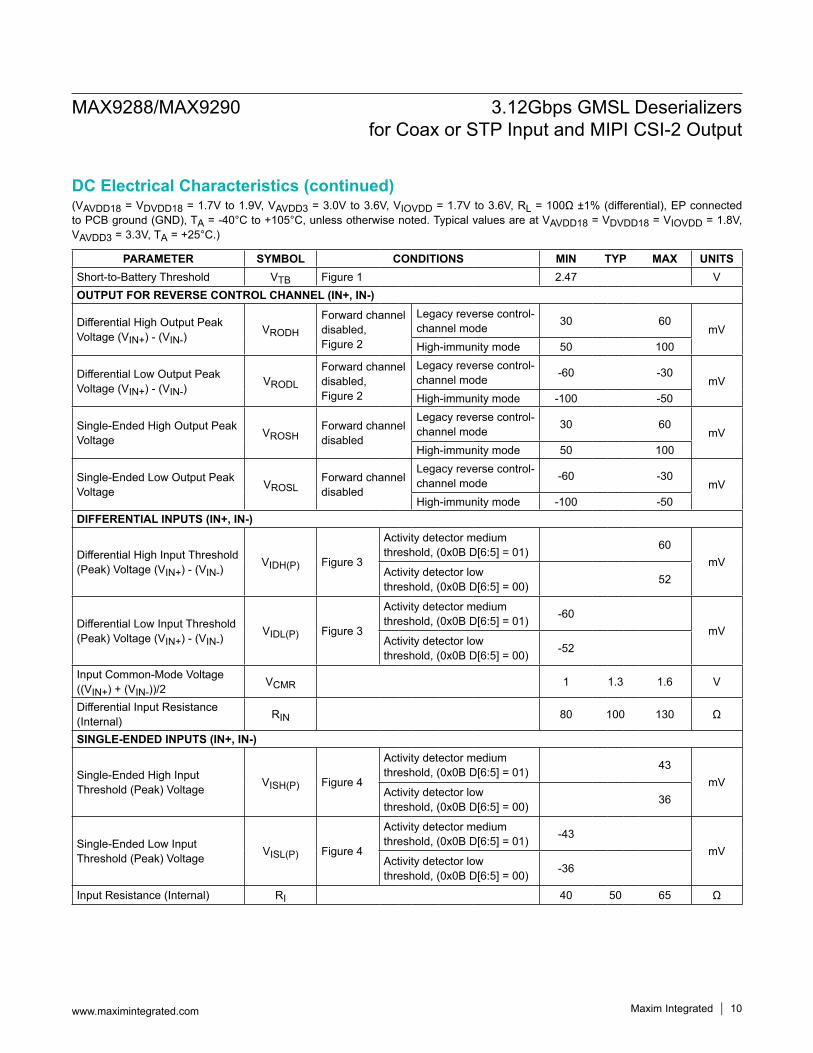
PARAMETER SYMBOL CONDITIONS MIN TYP MAX UNITSShort-to-Battery Threshold VTB Figure 1 2.47 VOUTPUT FOR REVERSE CONTROL CHANNEL (IN+, IN-)
Differential High Output Peak Voltage (VIN+) - (VIN-)
VRODH
Forward channel disabled, Figure 2
Legacy reverse control-channel mode 30 60
mVHigh-immunity mode 50 100
Differential Low Output Peak Voltage (VIN+) - (VIN-)
VRODL
Forward channel disabled, Figure 2
Legacy reverse control-channel mode -60 -30
mVHigh-immunity mode -100 -50
Single-Ended High Output Peak Voltage VROSH
Forward channel disabled
Legacy reverse control-channel mode 30 60
mVHigh-immunity mode 50 100
Single-Ended Low Output Peak Voltage VROSL
Forward channel disabled
Legacy reverse control-channel mode -60 -30
mVHigh-immunity mode -100 -50
DIFFERENTIAL INPUTS (IN+, IN-)
Differential High Input Threshold (Peak) Voltage (VIN+) - (VIN-)
VIDH(P) Figure 3
Activity detector medium threshold, (0x0B D[6:5] = 01) 60
mVActivity detector low threshold, (0x0B D[6:5] = 00) 52
Differential Low Input Threshold (Peak) Voltage (VIN+) - (VIN-)
VIDL(P) Figure 3
Activity detector medium threshold, (0x0B D[6:5] = 01) -60
mVActivity detector low threshold, (0x0B D[6:5] = 00) -52
Input Common-Mode Voltage ((VIN+) + (VIN-))/2
VCMR 1 1.3 1.6 V
Differential Input Resistance (Internal) RIN 80 100 130 Ω
SINGLE-ENDED INPUTS (IN+, IN-)
Single-Ended High Input Threshold (Peak) Voltage VISH(P) Figure 4
Activity detector medium threshold, (0x0B D[6:5] = 01) 43
mVActivity detector low threshold, (0x0B D[6:5] = 00) 36
Single-Ended Low Input Threshold (Peak) Voltage VISL(P) Figure 4
Activity detector medium threshold, (0x0B D[6:5] = 01) -43
mVActivity detector low threshold, (0x0B D[6:5] = 00) -36
Input Resistance (Internal) RI 40 50 65 Ω
DC Electrical Characteristics (continued)
(VAVDD18 = VDVDD18 = 1.7V to 1.9V, VAVDD3 = 3.0V to 3.6V, VIOVDD = 1.7V to 3.6V, RL = 100Ω ±1% (differential), EP connected to PCB ground (GND), TA = -40°C to +105°C, unless otherwise noted. Typical values are at VAVDD18 = VDVDD18 = VIOVDD = 1.8V, VAVDD3 = 3.3V, TA = +25°C.) (Note 3)
MAX9288/MAX9290 3.12Gbps GMSL Deserializers for Coax or STP Input and MIPI CSI-2 Output
www.maximintegrated.com Maxim Integrated 11
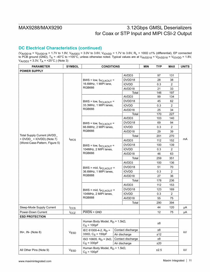
PARAMETER SYMBOL CONDITIONS MIN TYP MAX UNITSPOWER SUPPLY
Total Supply Current (AVDD_ + DVDD_ + IOVDD) (Note 7) (Worst-Case-Pattern, Figure 5)
IWCS
BWS = low, fPCLKOUT = 16.6MHz, 1 MIPI lane, RGB666
AVDD3 97 131
mA
DVDD18 28 38IOVDD 0.3 2AVDD18 21 33
Total 146 197
BWS = low, fPCLKOUT = 33.3MHz, 1 MIPI lanes, RGB666
AVDD3 99 134DVDD18 45 62IOVDD 0.3 2AVDD18 25 34
Total 170 227
BWS = low, fPCLKOUT = 66.6MHz, 2 MIPI lanes, RGB666
AVDD3 103 140DVDD18 69 94IOVDD 0.3 2AVDD18 29 39
Total 201 270
BWS = low, fPCLKOUT = 104MHz, 2 MIPI lanes, RGB666
AVDD3 112 152DVDD18 100 139IOVDD 0.3 2AVDD18 46 63
Total 259 351
BWS = mid, fPCLKOUT = 36.6MHz, 1 MIPI lanes, RGB888
AVDD3 100 136DVDD18 51 70IOVDD 0.3 2AVDD18 27 36
Total 178 236
BWS = mid, fPCLKOUT = 104MHz, 2 MIPI lanes, RGB888
AVDD3 112 153DVDD18 123 169IOVDD 0.3 2AVDD18 55 75
Total 290 394Sleep-Mode Supply Current ICCS 44 120 µAPower-Down Current ICCZ PWDN = GND 12 75 µAESD PROTECTION
IN+, IN- (Note 8) VESD
Human Body Model, RD = 1.5kΩ, CS = 100pF ±8
kVIEC 61000-4-2, RD = 330Ω, CS = 150pF
Contact discharge ±8Air discharge ±12
ISO 10605, RD = 2kΩ, CS = 330pF
Contact discharge ±8Air discharge ±20
All Other Pins (Note 9) VESDHuman Body Model, RD = 1.5kΩ, CS = 100pF ±2.5 kV
DC Electrical Characteristics (continued)
(VAVDD18 = VDVDD18 = 1.7V to 1.9V, VAVDD3 = 3.0V to 3.6V, VIOVDD = 1.7V to 3.6V, RL = 100Ω ±1% (differential), EP connected to PCB ground (GND), TA = -40°C to +105°C, unless otherwise noted. Typical values are at VAVDD18 = VDVDD18 = VIOVDD = 1.8V, VAVDD3 = 3.3V, TA = +25°C.)
MAX9288/MAX9290 3.12Gbps GMSL Deserializers for Coax or STP Input and MIPI CSI-2 Output
www.maximintegrated.com Maxim Integrated 12
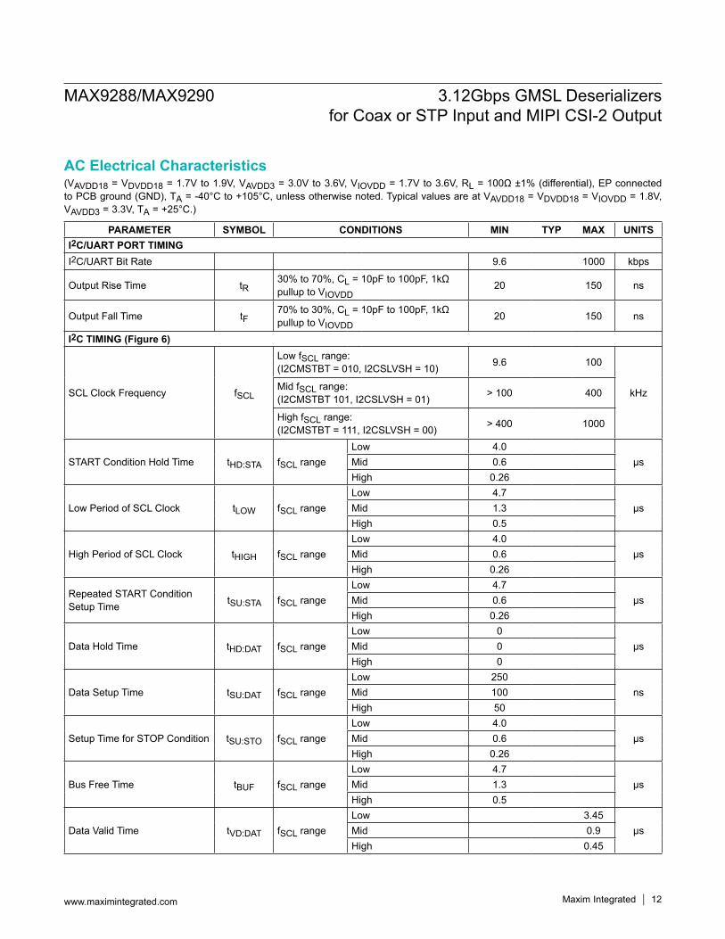
PARAMETER SYMBOL CONDITIONS MIN TYP MAX UNITSI2C/UART PORT TIMINGI2C/UART Bit Rate 9.6 1000 kbps
Output Rise Time tR30% to 70%, CL = 10pF to 100pF, 1kΩ pullup to VIOVDD
20 150 ns
Output Fall Time tF70% to 30%, CL = 10pF to 100pF, 1kΩ pullup to VIOVDD
20 150 ns
I2C TIMING (Figure 6)
SCL Clock Frequency fSCL
Low fSCL range:(I2CMSTBT = 010, I2CSLVSH = 10) 9.6 100
kHzMid fSCL range:(I2CMSTBT 101, I2CSLVSH = 01) > 100 400
High fSCL range:(I2CMSTBT = 111, I2CSLVSH = 00) > 400 1000
START Condition Hold Time tHD:STA fSCL rangeLow 4.0
µsMid 0.6High 0.26
Low Period of SCL Clock tLOW fSCL range Low 4.7
µsMid 1.3High 0.5
High Period of SCL Clock tHIGH fSCL rangeLow 4.0
µsMid 0.6High 0.26
Repeated START Condition Setup Time tSU:STA fSCL range
Low 4.7µsMid 0.6
High 0.26
Data Hold Time tHD:DAT fSCL rangeLow 0
µsMid 0High 0
Data Setup Time tSU:DAT fSCL rangeLow 250
nsMid 100High 50
Setup Time for STOP Condition tSU:STO fSCL rangeLow 4.0
µsMid 0.6High 0.26
Bus Free Time tBUF fSCL rangeLow 4.7
µsMid 1.3High 0.5
Data Valid Time tVD:DAT fSCL rangeLow 3.45
µsMid 0.9High 0.45
AC Electrical Characteristics
(VAVDD18 = VDVDD18 = 1.7V to 1.9V, VAVDD3 = 3.0V to 3.6V, VIOVDD = 1.7V to 3.6V, RL = 100Ω ±1% (differential), EP connected to PCB ground (GND), TA = -40°C to +105°C, unless otherwise noted. Typical values are at VAVDD18 = VDVDD18 = VIOVDD = 1.8V, VAVDD3 = 3.3V, TA = +25°C.)
MAX9288/MAX9290 3.12Gbps GMSL Deserializers for Coax or STP Input and MIPI CSI-2 Output
www.maximintegrated.com Maxim Integrated 13
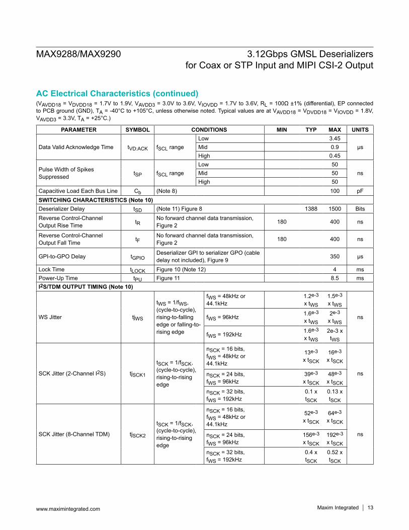
PARAMETER SYMBOL CONDITIONS MIN TYP MAX UNITS
Data Valid Acknowledge Time tVD:ACK fSCL rangeLow 3.45
µsMid 0.9High 0.45
Pulse Width of Spikes Suppressed tSP fSCL range
Low 50nsMid 50
High 50Capacitive Load Each Bus Line Cb (Note 8) 100 pFSWITCHING CHARACTERISTICS (Note 10)Deserializer Delay tSD (Note 11) Figure 8 1388 1500 BitsReverse Control-Channel Output Rise Time tR
No forward channel data transmission, Figure 2 180 400 ns
Reverse Control-Channel Output Fall Time tF
No forward channel data transmission, Figure 2 180 400 ns
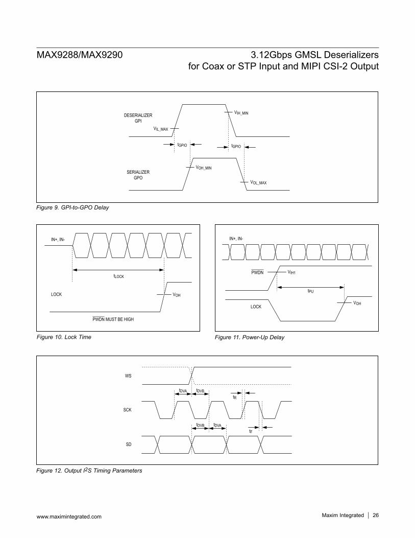
GPI-to-GPO Delay tGPIODeserializer GPI to serializer GPO (cable delay not included), Figure 9 350 µs
Lock Time tLOCK Figure 10 (Note 12) 4 msPower-Up Time tPU Figure 11 8.5 msI2S/TDM OUTPUT TIMING (Note 10)
WS Jitter tjWS
tWS = 1/fWS, (cycle-to-cycle), rising-to-falling edge or falling-to-rising edge
fWS = 48kHz or 44.1kHz
1.2e-3 x tWS
1.5e-3 x tWS
nsfWS = 96kHz 1.6e-3
x tWS
2e-3
x tWS
fWS = 192kHz 1.6e-3
x tWS
2e-3 x tWS
SCK Jitter (2-Channel I2S) tjSCK1
tSCK = 1/fSCK, (cycle-to-cycle), rising-to-rising edge
nSCK = 16 bits,fWS = 48kHz or 44.1kHz
13e-3
x tSCK
16e-3
x tSCK
nsnSCK = 24 bits,fWS = 96kHz
39e-3
x tSCK
48e-3
x tSCK
nSCK = 32 bits,fWS = 192kHz
0.1 x tSCK
0.13 x tSCK
SCK Jitter (8-Channel TDM) tjSCK2
tSCK = 1/fSCK, (cycle-to-cycle), rising-to-rising edge
nSCK = 16 bits,fWS = 48kHz or 44.1kHz
52e-3
x tSCK
64e-3
x tSCK
nsnSCK = 24 bits,fWS = 96kHz
156e-3
x tSCK
192e-3
x tSCK
nSCK = 32 bits,fWS = 192kHz
0.4 x tSCK
0.52 x tSCK
AC Electrical Characteristics (continued)
(VAVDD18 = VDVDD18 = 1.7V to 1.9V, VAVDD3 = 3.0V to 3.6V, VIOVDD = 1.7V to 3.6V, RL = 100Ω ±1% (differential), EP connected to PCB ground (GND), TA = -40°C to +105°C, unless otherwise noted. Typical values are at VAVDD18 = VDVDD18 = VIOVDD = 1.8V, VAVDD3 = 3.3V, TA = +25°C.)
MAX9288/MAX9290 3.12Gbps GMSL Deserializers for Coax or STP Input and MIPI CSI-2 Output
www.maximintegrated.com Maxim Integrated 14
PARAMETER SYMBOL CONDITIONS MIN TYP MAX UNITS
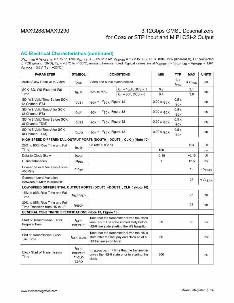
Audio Skew Relative to Video tASK Video and audio synchronized 3 x tWS
4 x tWS µs
SCK, SD, WS Rise-and-Fall Time tR, tF 20% to 80%
CL = 10pF, DCS = 1 0.3 3.1ns
CL = 5pF, DCS = 0 0.4 3.8SD, WS Valid Time Before SCK (2-Channel I2S) tDVB1 tSCK = 1/fSCK, Figure 12 0.20 x tSCK
0.5 x tSCK
ns
SD, WS Valid Time After SCK (2-Channel I2S) tDVA1 tSCK = 1/fSCK, Figure 12 0.20 x tSCK
0.5 x tSCK
ns
SD, WS Valid Time Before SCK (8-Channel TDM) tDVB2 tSCK = 1/fSCK, Figure 12 0.20 x tSCK
0.5 x tSCK
ns
SD, WS Valid Time After SCK (8-Channel TDM) tDVA2 tSCK = 1/fSCK, Figure 12 0.20 x tSCK
0.5 x tSCK
ns
HIGH-SPEED DIFFERENTAIL OUTPUT PORTS (DOUT0_–DOUT3_, CLK_) (Note 10)20% to 80% Rise Time and Fall Time tR, tF
Bit rate ≤ 1Gbps 0.3 UI100 ps
Data-to-Clock Skew tSKW -0.15 +0.15 UIUI Instantaneous UIINS 1 12.5 ns
Common-Level Variation Above 450MHz ΔVCM 15 mVRMS
Common-Level Variation Between 50MHz to 450MHz 25 mVPEAK
LOW-SPEED DIFFERENTIAL OUTPUT PORTS (DOUT0_–DOUT3_, CLK_) (Note 10)15% to 85% Rise Time and Fall Time tRLP/tFLP 25 ns
30% to 85% Rise Time and Fall Time Transition from HS to LP tREOP 35 ns
GENERAL CSI-2 TIMING SPECIFICATIONS (Note 10, Figure 13)
Start of Transmission: Clock Prepare Time
tCLK-PREPARE
Time that the transmitter drives the clock lane LP-00 line state immediately before HS-0 line state starting the HS transition
38 95 ns
End of Transmission: Clock Trail Time tCLK-TRAIL
Time that the transmitter drives the HS-0 state after the last payload clock bit of a HS transmission burst
60 ns
Clock Start of Transmission Time
tCLK-PREPARE + tCLK-ZERO
tCLK-PREPARE + time that the transmitter drives the HS-0 state prior to starting the clock
300 ns
AC Electrical Characteristics (continued)
(VAVDD18 = VDVDD18 = 1.7V to 1.9V, VAVDD3 = 3.0V to 3.6V, VIOVDD = 1.7V to 3.6V, RL = 100Ω ±1% (differential), EP connected to PCB ground (GND), TA = -40°C to +105°C, unless otherwise noted. Typical values are at VAVDD18 = VDVDD18 = VIOVDD = 1.8V, VAVDD3 = 3.3V, TA = +25°C.)
Note 3: Limits are 100% production tested at TA = +105°C. Limits over the operating temperature range are guaranteed by design and characterization, unless otherwise noted.
Note 4: To provide a mid level, leave the input open, or, if driven, put driver in high impedance. High-impedance leakage current must be less than ±10µA.
Note 5: IIN_ min due to voltage drop across the internal pullup resistor.Note 6: Not production tested. Guaranteed by design.Note 7: HDCP enabled (MAX9290 only). IOVDD current is not production tested. For the MAX9288 (or when HDCP is disabled on
the MAX9290), subtract the HDCP supply current, as shown in Table 25.Note 8: Specified pin to ground.Note 9: Specified pin to all supply/ground.Note 10: Not production tested, guaranteed by characterization.Note 11: Measured in serial link bit times. Bit time = 1/(30 x fPIXEL) for BWS = 0 or open. Bit time = 1/(40 x fPIXEL)
for BWS = 1.
MAX9288/MAX9290 3.12Gbps GMSL Deserializers for Coax or STP Input and MIPI CSI-2 Output
www.maximintegrated.com Maxim Integrated 15
PARAMETER SYMBOL CONDITIONS MIN TYP MAX UNITS
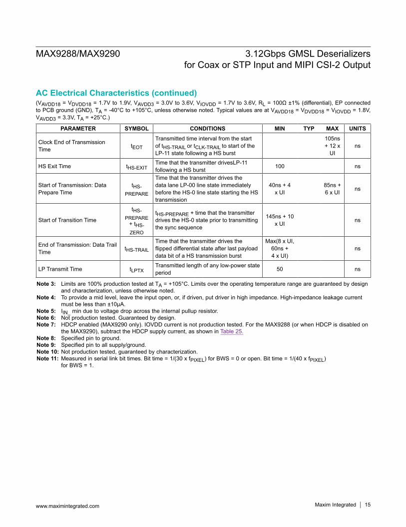
Clock End of Transmission Time tEOT
Transmitted time interval from the start of tHS-TRAIL or tCLK-TRAIL to start of the LP-11 state following a HS burst
105ns + 12 x
UIns
HS Exit Time tHS-EXITTime that the transmitter drivesLP-11 following a HS burst 100 ns
Start of Transmission: Data Prepare Time
tHS-PREPARE
Time that the transmitter drives the data lane LP-00 line state immediately before the HS-0 line state starting the HS transmission
40ns + 4 x UI
85ns + 6 x UI ns
Start of Transition Time
tHS-PREPARE
+ tHS-ZERO
tHS-PREPARE + time that the transmitter drives the HS-0 state prior to transmitting the sync sequence
145ns + 10 x UI ns
End of Transmission: Data Trail Time tHS-TRAIL
Time that the transmitter drives the flipped differential state after last payload data bit of a HS transmission burst
Max(8 x UI, 60ns + 4 x UI)
ns
LP Transmit Time tLPTXTransmitted length of any low-power state period 50 ns
AC Electrical Characteristics (continued)
(VAVDD18 = VDVDD18 = VIOVDD = 1.8V, VAVDD3 = 3.3V, TA = +25°C, unless otherwise noted.)
MAX9288/MAX9290 3.12Gbps GMSL Deserializers for Coax or STP Input and MIPI CSI-2 Output
Maxim Integrated 16www.maximintegrated.com
100
120
140
160
180
200
220
240
260
15 30 45 60 75 90 105
SUPP
LY C
URRE
NT (m
A)
PCLK FREQUENCY (MHz)
SUPPLY CURRENTvs. PIXEL CLOCK FREQUENCY (BWS = OPEN)
toc02
PRBS ON, COAX MODE,
RGB888, HDCP ON
2 CHANNELS
EQ OFF
EQ ON
100
120
140
160
180
200
220
240
260
5 20 35 50 65 80
SUPP
LY C
URRE
NT (m
A)
PCLK FREQUENCY (MHz)
SUPPLY CURRENTvs. PIXEL CLOCK FREQUENCY (BWS = HIGH)
toc03
PRBS ON,COAX MODE,
RGB888,HDCP ON
2 CHANNELS
EQ OFF
EQ ON
100
120
140
160
180
200
220
240
260
5 15 25 35 45 55 65 75 85 95 105
SUPP
LY C
URRE
NT (m
A)
PCLK FREQUENCY (MHz)
SUPPLY CURRENTvs. PIXEL CLOCK FREQUENCY (BWS = LOW)
toc01
PRBS ON,COAX MODE,
RGB666,HDCP ON
2 CHANNELS
EQ OFF
EQ ON
100
120
140
160
180
200
220
240
260
5 15 25 35 45 55 65 75 85 95 105
SUPP
LY C
URRE
NT (m
A)
PCLK FREQUENCY (MHz)
SUPPLY CURRENTvs. PIXEL CLOCK FREQUENCY (BWS = LOW)
toc04
PRBS ON,COAX MODE,
RGB666,HDCP ON
4 CHANNELS
EQ OFF
EQ ON
100
120
140
160
180
200
220
240
260
5 20 35 50 65 80
SUPP
LY C
URRE
NT (m
A)
PCLK FREQUENCY (MHz)
SUPPLY CURRENTvs. PIXEL CLOCK FREQUENCY (BWS = HIGH)
toc06
PRBS ON,COAX MODE,
RGB888,HDCP ON
4 CHANNELS
EQ OFF
EQ ON
100
120
140
160
180
200
220
240
260
15 30 45 60 75 90 105
SUPP
LY C
URRE
NT (m
A)
PCLK FREQUENCY (MHz)
SUPPLY CURRENTvs. PIXEL CLOCK FREQUENCY (BWS = OPEN)
toc05
PRBS ON, COAX MODE,
RGB888, HDCP ON
4 CHANNELS
EQ OFF
EQ ON
0
20
40
60
80
100
120
0 5 10 15 20 25
PIXE
L CLO
CK F
REQU
ENCY
(MHz
)
CABLE LENGTH (m)
MAXIMUM PIXEL CLOCK FREQUENCYvs. COAX CABLE LENGTH (BER ≤ 10-10)
toc07
BER CAN BE AS LOW AS 10-12 FOR CABLE LENGTHS LESS THAN 15m
OPTIMUM PE/EQ
NO PE, 10.7dB EQ
NO PE/EQ
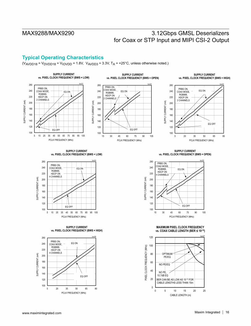
Typical Operating Characteristics
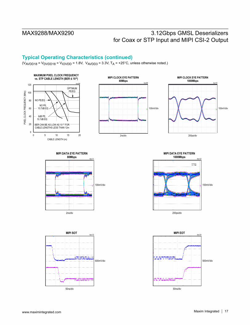
(VAVDD18 = VDVDD18 = VIOVDD = 1.8V, VAVDD3 = 3.3V, TA = +25°C, unless otherwise noted.)
MAX9288/MAX9290 3.12Gbps GMSL Deserializers for Coax or STP Input and MIPI CSI-2 Output
Maxim Integrated 17www.maximintegrated.com
100mV/div
toc09
2ns/div
MIPI CLOCK EYE PATTERN80Mbps
100mV/div
toc10
200ps/div
MIPI CLOCK EYE PATTERN1000Mbps
0
20
40
60
80
100
120
0 5 10 15 20
PIXE
L CLO
CK F
REQU
ENCY
(MHz
)
CABLE LENGTH (m)
MAXIMUM PIXEL CLOCK FREQUENCYvs. STP CABLE LENGTH (BER ≤ 10-9)
toc08
BER CAN BE AS LOW AS 10-12 FOR CABLE LENGTHS LESS THAN 12m
OPTIMUM PE/EQ
NO PE, 10.7dB EQ
NO PE/EQ
6dB PE, 10.7dB EQ
100mV/div
toc11
2ns/div
MIPI DATA EYE PATTERN80Mbps
500mV/div
toc13
50ns/div
MIPI SOT
100mV/div
toc12
200ps/div
MIPI DATA EYE PATTERN1000Mbps
500mV/div
toc14
50ns/div
MIPI EOT
Typical Operating Characteristics (continued)
MAX9288/MAX9290 3.12Gbps GMSL Deserializers for Coax or STP Input and MIPI CSI-2 Output
www.maximintegrated.com Maxim Integrated 18
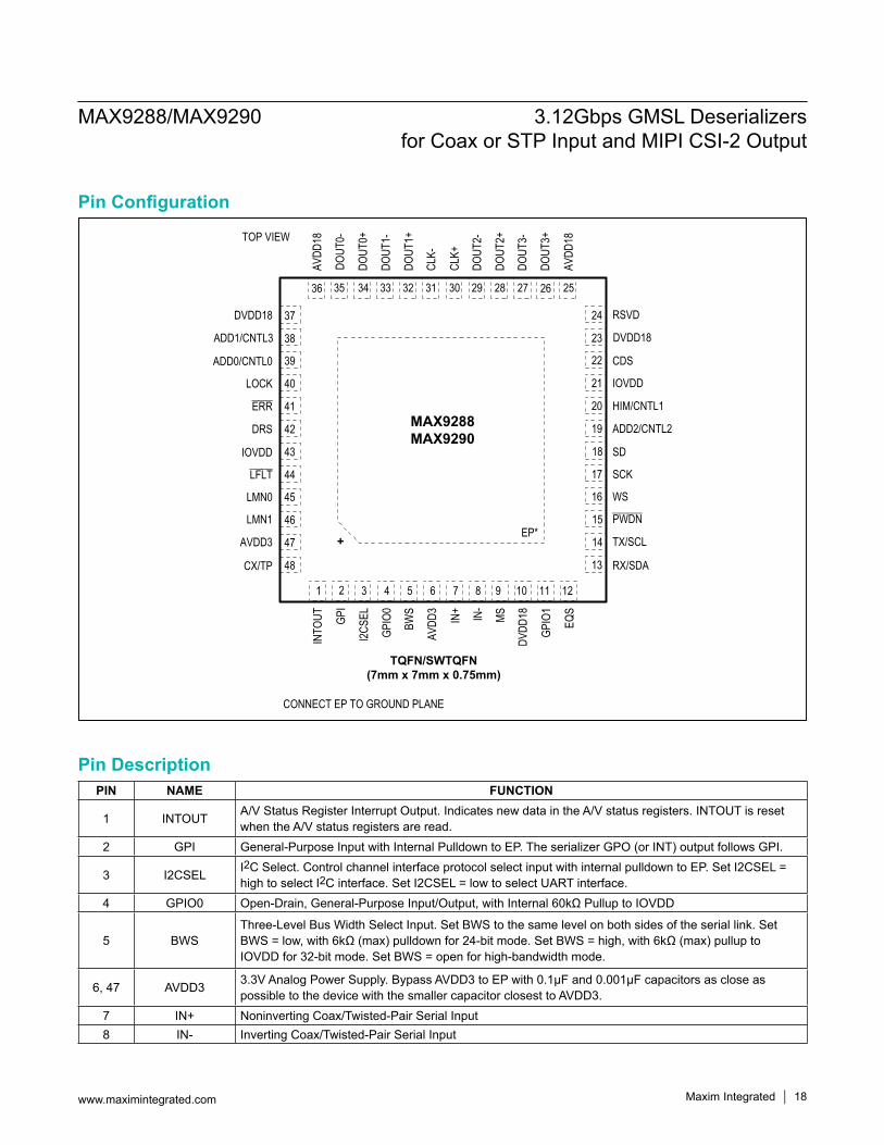
PIN NAME FUNCTION
1 INTOUT A/V Status Register Interrupt Output. Indicates new data in the A/V status registers. INTOUT is reset when the A/V status registers are read.
2 GPI General-Purpose Input with Internal Pulldown to EP. The serializer GPO (or INT) output follows GPI.
3 I2CSEL I2C Select. Control channel interface protocol select input with internal pulldown to EP. Set I2CSEL = high to select I2C interface. Set I2CSEL = low to select UART interface.
4 GPIO0 Open-Drain, General-Purpose Input/Output, with Internal 60kΩ Pullup to IOVDD
5 BWSThree-Level Bus Width Select Input. Set BWS to the same level on both sides of the serial link. Set BWS = low, with 6kΩ (max) pulldown for 24-bit mode. Set BWS = high, with 6kΩ (max) pullup to IOVDD for 32-bit mode. Set BWS = open for high-bandwidth mode.
6, 47 AVDD3 3.3V Analog Power Supply. Bypass AVDD3 to EP with 0.1µF and 0.001µF capacitors as close as possible to the device with the smaller capacitor closest to AVDD3.
7 IN+ Noninverting Coax/Twisted-Pair Serial Input8 IN- Inverting Coax/Twisted-Pair Serial Input
TQFN/SWTQFN (7mm x 7mm x 0.75mm)
CONNECT EP TO GROUND PLANE
EP*
MAX9288MAX9290
TOP VIEW
13
14
15
16
17
18
19
20
21
22
23
24
RX/SDA
+ TX/SCL
PWDN
WS
SCK
SD
ADD2/CNTL2
HIM/CNTL1
IOVDD
CDS
DVDD18
RSVD
48
47
46
45
44
43
42
41
40
39
38
37
1 2 3 4 5 6 7 8 9 10 11 12
CX/TP
AVDD3
LMN1
LMN0
LFLT
IOVDD
DRS
ERR
LOCK
ADD0/CNTL0
ADD1/CNTL3
DVDD18
EQS
GPIO
1
DVDD
18MSIN-
IN+
AVDD
3
BWS
GPIO
0
I2CSE
L
GPI
INTO
UT
36 35 34 33 32 31 30 29 28 27 26 25
AVDD
18
DOUT
3+
DOUT
3-
DOUT
2+
DOUT
2-
CLK+
CLK-
DOUT
1+
DOUT
1-
DOUT
0+
DOUT
0-
AVDD
18
Pin Description
Pin Configuration
MAX9288/MAX9290 3.12Gbps GMSL Deserializers for Coax or STP Input and MIPI CSI-2 Output
www.maximintegrated.com Maxim Integrated 19
PIN NAME FUNCTION
9 MSMode Select with Internal Pulldown to EP. MS sets the control-link mode when CDS = high. Set MS = low, to select base mode. Set MS = high to select the bypass mode. MS sets autostart mode when CDS = low.
10, 23, 37 DVDD18 1.8V Digital Power Supply. Bypass DVDD18 to EP with 0.1µF and 0.001µF capacitors as close as
possible to the device with the smaller value capacitor closest to DVDD18.11 GPIO1 Open-Drain, General-Purpose Input/Output, with Internal 60kΩ Pullup to IOVDD
12 EQS
Equalizer Select Input, with Internal Pulldown to EP. The state of EQS latches upon power-up or when resuming from power-down mode (PWDN = low). Leave EQS open for 10.7dB equalizer boost (EQTUNE = 1001). Connect EQS to IOVDD with a 30kΩ resistor for 5.2dB equalizer boost (EQTUNE = 0100).
13 RX/SDA
UART Receive/I2C Serial Data Input/Output, with Internal 30kΩ Pullup to IOVDD. Function is determined by the state of I2CSEL at power-up. RX/SDA has an open-drain driver and requires a pullup resistor.RX: Input of the deserializer’s UART.SDA: Data input/output of the deserializer’s I2C Master/Slave.
14 TX/SCL
UART Transmit/I2C Serial Clock Input/Output, with Internal 30kΩ Pullup to IOVDD. Function is determined by the state of I2CSEL at power-up. TX/SCL has an open-drain driver and requires a pullup resistor.TX: Output of the deserializer’s UART.SCL: Clock input/output of the deserializer’s I2C Master/Slave.
15 PWDN Active-Low, Power-Down Input, with Internal Pulldown to EP. Set PWDN low to enter power-down mode to reduce power consumption.
16 WSI2S/TDM Word-Select Input/Output. Powers up as an I2S output (deserializer provided clock). Set AUDIOMODE bit = ‘1’ to change WS to an input with internal pulldown to GND and supply WS externally (system provided clock).
17 SCKI2S/TDM Serial-Clock Input/Output. Powers up as an I2S output (deserializer provided clock). Set AUDIOMODE bit = ‘1’ to change SCK to an input with internal pulldown to GND and supply SCK externally (system provided clock).
18 SD I2S/TDM Serial-Data Output. Disable I2S/TDM encoding to serial data to use SD as an additional control/data output. Encrypted when HDCP is enabled.
19 ADD2/CNTL2
Address Selection Input/Auxiliary Control Signal Output, with Internal Pulldown to EP. Functions as ADD2 input at power-up or when resuming from power-down mode (PWDN = low), and switches to CNTL2 output automatically after power-up.
ADD2: Bit value is latched at power-up or when resuming from power-down mode (PWDN = low). See Table 1. Connect ADD2/CNTL2 to IOVDD with a 30kΩ resistor to set high or leave open to set low.
CNTL2: Used only in 32-bit and high-bandwidth mode (BWS = high, open). CNTL2 is mapped from the GMSL serializer’s CNTL2 or DIN28 input.
Pin Description (continued)
MAX9288/MAX9290 3.12Gbps GMSL Deserializers for Coax or STP Input and MIPI CSI-2 Output
www.maximintegrated.com Maxim Integrated 20
PIN NAME FUNCTION
20 HIM/CNTL1
High-Immunity Mode Input/Auxiliary Control Signal Output With Internal Pulldown to EP. Functions as HIM input at power-up or when resuming from power-down mode (PWDN = low), and switches to CNTL2 output automatically after power-up.
HIM: Default HIGHIMM bit value is latched at power-up or when resuming from power-down mode (PWDN = low) and is active-high. Connect HIM/CNTL1 to IOVDD with a 30kΩ resistor to set high or leave open to set low. HIGHIMM can be programmed to a different value after power-up. HIGHIMM in the serializer must be set to the same value.
CNTL1: Used only in 32-bit and high-bandwidth mode (BWS = high, open). CNTL1 is mapped from the GMSL serializer’s CNTL1, DIN27, or RES input.
21, 43 IOVDD I/O Supply Voltage. 1.8V to 3.3V logic I/O power supply. Bypass IOVDD to EP with 0.1µF and 0.001µF capacitors as close as possible to the device with the smallest value capacitor closest to IOVDD.
22 CDSControl Direction Selection Input, with Internal Pulldown to EP. Control link direct selection input with internal pulldown to EP. Set CDS = low when the control channel master µC is connected at the serializer. Set CDS = high when the control channel master µC is connected at the deserializer.
24 RES Reserved. Leave unconnected
25, 36 AVDD18 1.8V Analog Power Supply. Bypass AVDD18 to EP with 0.1µF and 0.001µF capacitors as close as possible to the device with the smaller capacitor closest to AVDD18.
26–29, 32–35
DOUT_+, DOUT_- CSI-2 Data Outputs
30, 31 CLK+, CLK- CSI-2 Clock Output
38 ADD1/CNTL3
Auxiliary Control Signal Output/Address Selection Input, with Internal Pulldown to EP. Functions as ADD1 input at power-up or when resuming from power-down mode (PWDN = low), and switches to CNTL3 output automatically after power-up.
ADD1: Bit value is latched at power-up or when resuming from power-down mode (PWDN = low). See Table 1. Connect ADD1/CNTL3 to IOVDD with a 30kΩ resistor to set high or leave open to set low.
CNTL3: Used only in high-bandwidth mode (BWS = open.
39 ADD0/CNTL0
Auxiliary Control Signal Output/Address Selection Input, with Internal Pulldown to EP. Functions as ADD0 input at power-up or when resuming from power-down mode (PWDN = low), and switches to CNTL0 output automatically after power-up.
ADD0: Bit value is latched at power-up or when resuming from power-down mode (PWDN = low). See Table 1. Connect ADD0/CNTL0 to IOVDD with a 30kΩ resistor to set high or leave open to set low.
CNTL0: Used only in high-bandwidth mode (BWS = open).
40 LOCKOpen-Drain Lock Output, with Internal 60kΩ Pullup to IOVDD. LOCK = high indicates that PLLs are locked with correct serial-word-boundary alignment. LOCK = low indicates that PLLs are not locked or an incorrect serial-word-boundary alignment. LOCK is high when PWDN = low.
41 ERR Error Output. Open-drain data error detection and/or correction indication output with internal 60kΩ pullup to IOVDD. ERR is high when PWDN is low.
Pin Description (continued)
MAX9288/MAX9290 3.12Gbps GMSL Deserializers for Coax or STP Input and MIPI CSI-2 Output
www.maximintegrated.com Maxim Integrated 21
PIN NAME FUNCTION
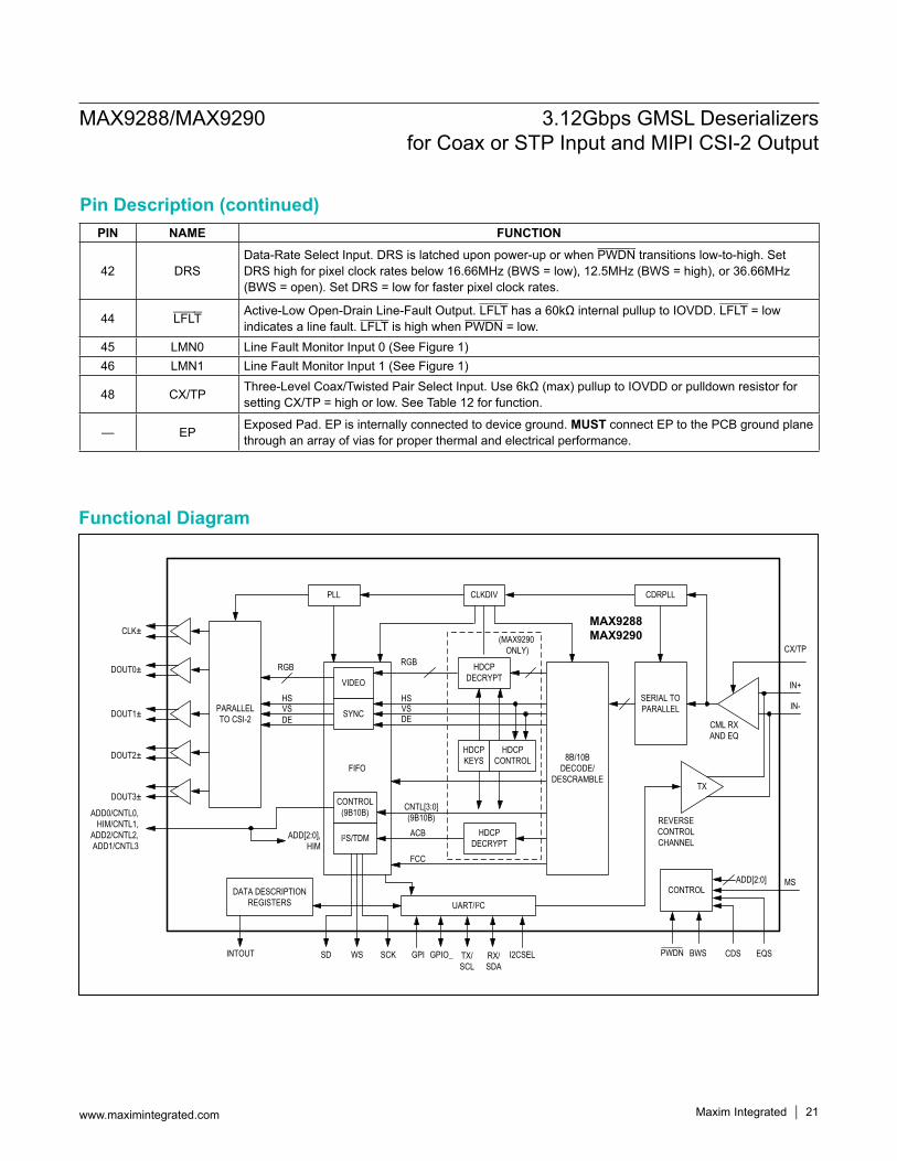
42 DRSData-Rate Select Input. DRS is latched upon power-up or when PWDN transitions low-to-high. Set DRS high for pixel clock rates below 16.66MHz (BWS = low), 12.5MHz (BWS = high), or 36.66MHz (BWS = open). Set DRS = low for faster pixel clock rates.
44 LFLT Active-Low Open-Drain Line-Fault Output. LFLT has a 60kΩ internal pullup to IOVDD. LFLT = low indicates a line fault. LFLT is high when PWDN = low.
45 LMN0 Line Fault Monitor Input 0 (See Figure 1)46 LMN1 Line Fault Monitor Input 1 (See Figure 1)
48 CX/TP Three-Level Coax/Twisted Pair Select Input. Use 6kΩ (max) pullup to IOVDD or pulldown resistor for setting CX/TP = high or low. See Table 12 for function.
— EP Exposed Pad. EP is internally connected to device ground. MUST connect EP to the PCB ground plane through an array of vias for proper thermal and electrical performance.
SERIAL TO PARALLEL
FIFO
PARALLEL TO CSI-2
I2S/TDM
TX
RGB
VSDE
HS
RGB
CNTL[3:0] (9B10B)
CLK±
DOUT0±
DOUT1±
DOUT2±
DOUT3±
PWDN BWS
REVERSE CONTROL CHANNEL
VIDEO
MAX9288MAX9290
IN+
IN-
CLKDIV
HDCP DECRYPT
VSDE
HS
HDCP DECRYPT
HDCP KEYS
CDRPLL
HDCP CONTROL
FCC
ACB
SD WS SCK
CML RX AND EQ
ADD[2:0]
8B/10B DECODE/
DESCRAMBLE
(MAX9290 ONLY)
CONTROL (9B10B)
SYNC
UART/I2C
TX/SCL
RX/SDA
GPIO_GPI I2CSEL
ADD0/CNTL0,HIM/CNTL1,
ADD2/CNTL2, ADD1/CNTL3
DATA DESCRIPTION REGISTERS
INTOUT
CONTROL
CX/TP
ADD[2:0], HIM
CDS EQS
MS
PLL
Pin Description (continued)
Functional Diagram
MAX9288/MAX9290 3.12Gbps GMSL Deserializers for Coax or STP Input and MIPI CSI-2 Output
www.maximintegrated.com Maxim Integrated 22
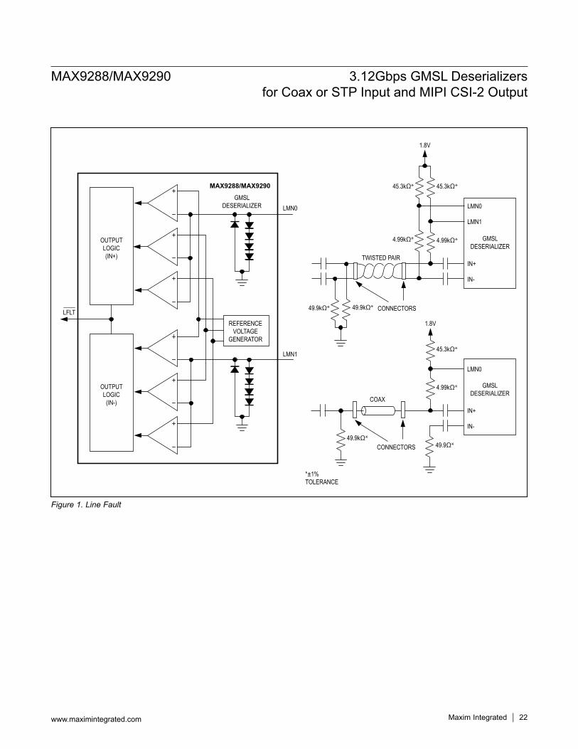
Figure 1. Line Fault
OUTPUTLOGIC(IN+)
OUTPUTLOGIC
(IN-)
REFERENCEVOLTAGE
GENERATOR
GMSLDESERIALIZER
MAX9288/MAX9290
GMSLDESERIALIZER
TWISTED PAIR
CONNECTORS
*±1%TOLERANCE
LFLT
LMN0
1.8V
LMN1
49.9kΩ*49.9kΩ*
LMN1
IN+
IN-
4.99kΩ*
45.3kΩ*45.3kΩ*
4.99kΩ*
LMN0
GMSLDESERIALIZER
COAX
CONNECTORS
1.8V
49.9kΩ*
IN+
IN-
45.3kΩ*
LMN0
4.99kΩ*
49.9Ω*
MAX9288/MAX9290 3.12Gbps GMSL Deserializers for Coax or STP Input and MIPI CSI-2 Output
www.maximintegrated.com Maxim Integrated 23
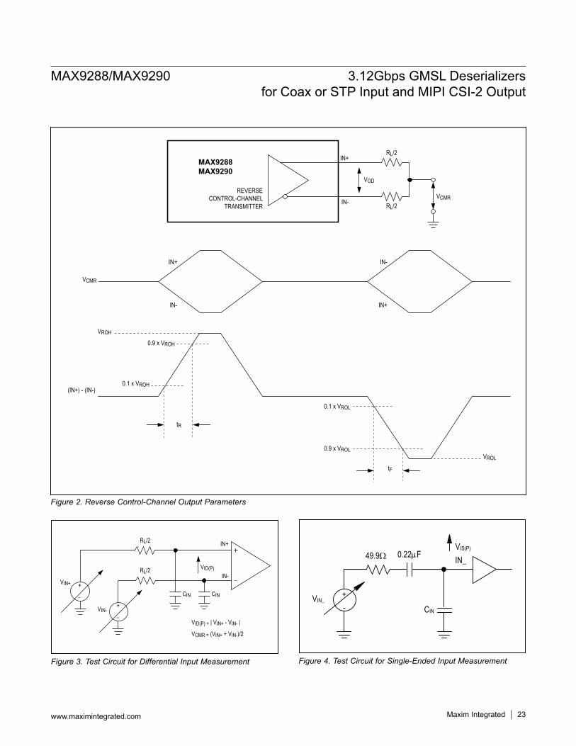
Figure 2. Reverse Control-Channel Output Parameters
Figure 3. Test Circuit for Differential Input Measurement
VIN+
RL/2
RL/2
CINCIN
VID(P)
IN+
IN-
VID(P) = | VIN+ - VIN- |
VCMR = (VIN+ + VIN-)/2
VIN-
_+
_
_+ CIN
0.22µF49.9Ω
+
-VIN_
IN_VIS(P)
MAX9288MAX9290
REVERSECONTROL-CHANNEL
TRANSMITTER
IN+
IN-
IN-
IN+
IN+
IN-
VOD
RL/2
RL/2
VCMR
VCMR
VROH
(IN+) - (IN-)
tR
0.1 x VROL
0.9 x VROL
tF
VROL
0.9 x VROH
0.1 x VROH
Figure 4. Test Circuit for Single-Ended Input Measurement
MAX9288/MAX9290 3.12Gbps GMSL Deserializers for Coax or STP Input and MIPI CSI-2 Output
www.maximintegrated.com Maxim Integrated 24
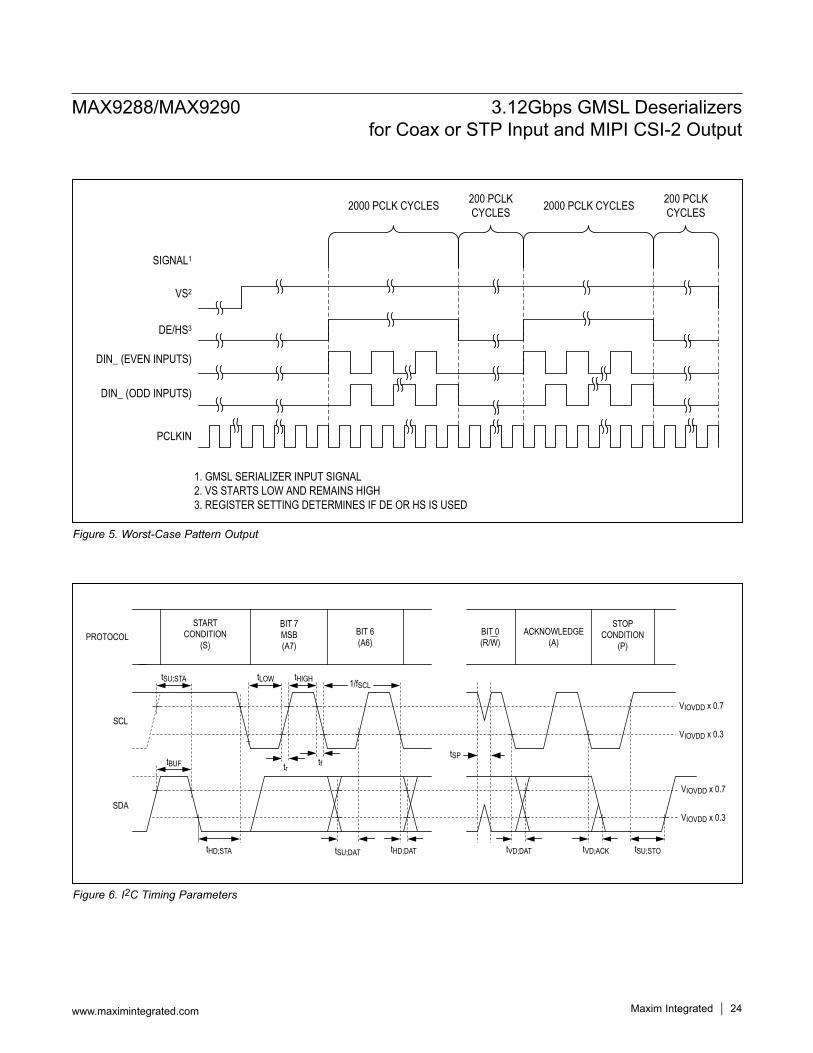
Figure 5. Worst-Case Pattern Output
Figure 6. I2C Timing Parameters
VS2
DE/HS3
DIN_ (EVEN INPUTS)
1. GMSL SERIALIZER INPUT SIGNAL2. VS STARTS LOW AND REMAINS HIGH3. REGISTER SETTING DETERMINES IF DE OR HS IS USED
DIN_ (ODD INPUTS)
SIGNAL1
2000 PCLK CYCLES
PCLKIN
200 PCLK CYCLES
200 PCLK CYCLES2000 PCLK CYCLES
PROTOCOL
SCL
SDA
STARTCONDITION
(S)
BIT 7MSB(A7)
BIT 6(A6)
BIT 0(R/W)
ACKNOWLEDGE(A)
STOPCONDITION
(P)
VIOVDD x 0.7
VIOVDD x 0.3
VIOVDD x 0.7
VIOVDD x 0.3
tSU;STA tLOW tHIGH
tBUF
tHD;STA
trtSP
tf
tSU;DAT tHD;DAT tVD;DAT tVD;ACK tSU;STO
1/fSCL
MAX9288/MAX9290 3.12Gbps GMSL Deserializers for Coax or STP Input and MIPI CSI-2 Output
www.maximintegrated.com Maxim Integrated 25
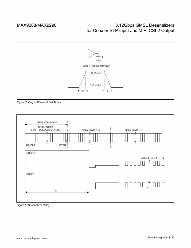
Figure 7. Output Rise-and-Fall Times
Figure 8. Deserializer Delay
0.8 x VI0VDD
0.2 x VI0VDD
tFtR
CL
SINGLE-ENDED OUTPUT LOAD
SERIAL WORD N(FIRST PIXEL WORD OF A LINE)
SERIAL BYTE N, N+1, N+2
LAST BITFIRST BIT
SERIAL WORD N+2SERIAL WORD N +1
SERIAL WORD LENGTH
tSD
TxDOUT+
TxDOUT-
MAX9288/MAX9290 3.12Gbps GMSL Deserializers for Coax or STP Input and MIPI CSI-2 Output
www.maximintegrated.com Maxim Integrated 26
Figure 10. Lock Time Figure 11. Power-Up Delay
Figure 12. Output I2S Timing Parameters
Figure 9. GPI-to-GPO Delay
WS
tDVA
tDVB tDVAtF
tDVBtR
SCK
SD
IN+, IN-
LOCK
tLOCK
PWDN MUST BE HIGH
VOH
IN+, IN-
LOCK
tPU
PWDN
VOH
VIH1
tGPIO tGPIO
VOH_MIN
VOL_MAX
VIH_MIN
VIL_MAX
DESERIALIZERGPI
SERIALIZERGPO
MAX9288/MAX9290 3.12Gbps GMSL Deserializers for Coax or STP Input and MIPI CSI-2 Output
www.maximintegrated.com Maxim Integrated 27
Detailed DescriptionThe MAX9288/MAX9290 deserializers, when paired with the MAX9275/MAX9277/MAX9279/MAX9281 serializ-ers, provide the full set of operating features, but are backward-compatible with the MAX9249–MAX9270 fam-ily of gigabit multimedia serial link (GMSL) devices, and have basic functionality when paired with any GMSL device. The MAX9290 has high-bandwidth digital content protection (HDCP), while the MAX9288 does not.Each deserializer has a maximum serial-bit rate of 3.12Gbps for up to 15m of cable and operates up to a maximum output clock of 104MHz in 24-bit mode and 27-bit high-bandwidth mode, or 78MHz in 32-bit mode. This bit rate and output flexibility support a wide range of displays, from QVGA (320 x 240) to 1920 x 720 and higher with 24-bit color, as well as megapixel image sen-sors. An encoded audio channel supports L-PCM I2S stereo and up to eight channels of L-PCM in TDM mode. Sample rates of 32kHz to 192kHz are supported with sample depth from 8 to 32 bits. Input equalization, com-bined with GMSL serializer pre/deemphasis, extends the cable length and enhances link reliability.
The control channel enables a µC to program the serial-izer and deserializer registers and program registers on peripherals. The control channel is also used to perform HDCP functions (MAX9290 only). The µC can be located at either end of the link, or when using two µCs, at both ends. Two modes of control-channel operation are avail-able. Base mode uses either I2C or GMSL UART protocol, while bypass mode uses a user-defined UART protocol. UART protocol allows full-duplex communication, while I2C allows half-duplex communication.The serial input complies with ISO 10605 and IEC 61000-4-2 ESD protection standards.
Register MappingRegisters set the operating conditions of the deserial-izers and are programmed using the control channel in base mode. The MAX9288/MAX9290 holds its own device address and the device address of the serial-izer it is paired with. Similarly, the serializer holds its own device address and the address of the MAX9288/MAX9290. Whenever a device address is changed, be sure to write the new address to both devices. The default device address of the deserializer is set by the ADD_ and CX/TP inputs (Table 1). Registers 0x00 and 0x01 in both devices hold the device addresses.
Figure 13. MIPI Output Timing Parameters
CLK+/-
DOUT_+/-VIL(max)VIH(min)
VIDTH(max)
CAPTURE 1ST DATA BIT
tLPTX tHS-PREPARE tHS-ZERO tHS-SYNC
LP-11 LP-01 LP-00
tD-TERM-EN
tHS-SETTLE
LP-11tHS-SKIP
tREOT
tEOTtHS-TRAIL tHS-EXIT
DISCONNECT TERMINATOR
VTERM-EN(max)
CLK+/-
VIL(max)
VIDTH(max)
tLPTX tCLK-PREPARE tCLK-ZERO
LP-11 LP-01 LP-00
TD-TERM-EN
tHS-SETTLE
VTERM-EN(max)
NOTE: THE CSI CLOCK RUNS IN CONTINUOUS MODE ONLY.
MAX9288/MAX9290 3.12Gbps GMSL Deserializers for Coax or STP Input and MIPI CSI-2 Output
www.maximintegrated.com Maxim Integrated 28
Output Bit MapThe input/output bit width depends on settings of the bus width pin (BWS) and the CSI-2 output mode. Table 4 and Table 3 list the bit map for video signals. Table 4 lists the bit map for control signals. Unused control output bits are pulled low.
Serial Link Signaling and Data FormatThe serializer uses differential CML signaling to drive twisted-pair cable and single-ended CML to drive coaxial cable with programmable pre/deemphasis and AC-coupling. The deserializer uses AC-coupling and programmable channel equalization.Input data is scrambled and then 8b/10b coded (9b/10b in high-bandwidth mode). The deserializer recovers the embedded serial clock, then samples, decodes, and descrambles the data. In 24-bit mode, the first 21 bits contain 18 bits of video data and 3 bits of control data (HS/VS/DE). In 32-bit mode, the first 29 bits contain 24 bits of video data, 3 bits of control data (HS/VS/DE) and two bits of control data (CNTL1/CNTL2). In high-bandwidth mode, the first 24 bits contain video data, or
special control-signal packets. In all modes, the last 3 bits contain the embedded audio channel, the embedded for-ward control channel, and the parity bit of the serial word (Figure 14, Figure 15, Figure 16).
GMSL-to-CSI-2 Conversion and OutputThe GMSL deserializer recovers the clock from the serialized input signals and extracts the video, audio, and control. Video data are packetized to according to MIPI CSI-2 packet formats and sent out through the MIPI DPHY serial lanes.
Video Data OperationThe device converts the video control signal VS to the CSI-2 Frame Start or Frame End short packet (Figure 17). The converter also assembles the pixel color data into the CSI-2 long packets based on the formats and/or pixel count programmed by the user (Figure 18, Figure 19, Figure 20, Figure 21, Figure 22, Figure 23, Figure 24, Figure 25, Figure 26, Figure 27, Figure 28, Figure 29, Figure 30, and Figure 31). DE low period needs to be a minimum 200 PCLK cycles to accommodate SOT and EOT during the DE blanking period.
Table 1. Device Address Defaults (Register 0x00, 0x01)
*X = 0 for the serializer address, X = 1 for the deserializer address.**CX/TP determine the serial-cable type CX/TP = open addresses only for coax mode.
PIN DEVICE ADDRESS(BIN)
SERIALIZERDEVICE
ADDRESS(hex)
DESERIALIZERDEVICE
ADDRESS(hex)CX/TP ADD2 ADD1 ADD0 D7 D6 D5 D4 D3 D2 D1 D0
High/Low Low Low Low 1 0 0 X* 0 0 0 R/W 80 90High/Low Low Low High 1 0 0 X* 0 1 0 R/W 84 94High/Low Low High Low 1 0 0 X* 1 0 0 R/W 88 98High/Low Low High High 0 1 0 X* 0 1 0 R/W 44 54High/Low High Low Low 1 1 0 X* 0 0 0 R/W C0 D0High/Low High Low High 1 1 0 X* 0 1 0 R/W C4 D4High/Low High High Low 1 1 0 X* 1 0 0 R/W C8 D8High/Low High High High 0 1 0 X* 1 0 0 R/W 48 58Open** Low Low Low 1 0 0 X* 0 0 X* R/W 80 92Open** Low Low High 1 0 0 X* 0 1 X* R/W 84 96Open** Low High Low 1 0 0 X* 1 0 X* R/W 88 9AOpen** Low High High 0 1 0 X* 0 1 X* R/W 44 56Open** High Low Low 1 1 0 X* 0 0 X* R/W C0 D2Open** High Low High 1 1 0 X* 0 1 X* R/W C4 D6Open** High High Low 1 1 0 X* 1 0 X* R/W C8 DAOpen** High High High 0 1 0 X* 1 0 X* R/W 48 5A
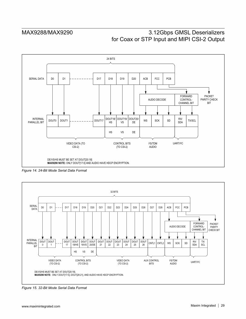
MAX9288/MAX9290 3.12Gbps GMSL Deserializers for Coax or STP Input and MIPI CSI-2 Output
www.maximintegrated.com Maxim Integrated 29
Figure 14. 24-Bit Mode Serial Data Format
Figure 15. 32-Bit Mode Serial Data Format
PACKET PARITY CHECK
BIT
ACB FCC PCBD0 D1
HS VS DE
D20D19D18D17
DE/VS/HS MUST BE SET AT DOUT[20:18]MAX9290 NOTE: ONLY DOUT[17:0] AND AUDIO HAVE HDCP ENCRYPTION.
VIDEO DATA (TO CSI-2)
CONTROL BITS (TO CSI-2)
DOUT0 DOUT1 DOUT17 DOUT18/HS
DOUT19/VS
DOUT20/DE
SERIAL DATA
INTERNAL PARALLEL BIT WS SCK SD RX/
SDA TX/SCL
AUDIO DECODE
I2S/TDM AUDIO
UART/I2C
FORWARD CONTROL-
CHANNEL BIT
24 BITS
DE/VS/HS MUST BE SET AT DOUT[20:18].MAX9290 NOTE: ONLY DOUT[17:0], DOUT[26:21], AND AUDIO HAVE HDCP ENCRYPTION.
D23
32 BITS
PACKET PARITY
CHECK BIT
D24 D25 D26 D27 D28 ACB FCC PCBD0 D1
HS VS DE
D22D21D20D19D18D17
VIDEO DATA (TO CSI-2)
CONTROL BITS (TO CSI-2)
VIDEO DATA (TO CSI-2)
AUX CONTROL BITS
DOUT0
DOUT1
DOUT17
DOUT18/HS
DOUT19/VS
DOUT20/DE
DOUT21
DOUT22
DOUT23
DOUT24
DOUT25
DOUT26 CNTL1 CNTL2
SERIALDATA
INTERNAL PARALLEL
BITWS SCK SD RX/
SDATX/SCL
AUDIO DECODE
I2S/TDM AUDIO UART/I2C
FORWARD CONTROL-
CHANNEL BIT
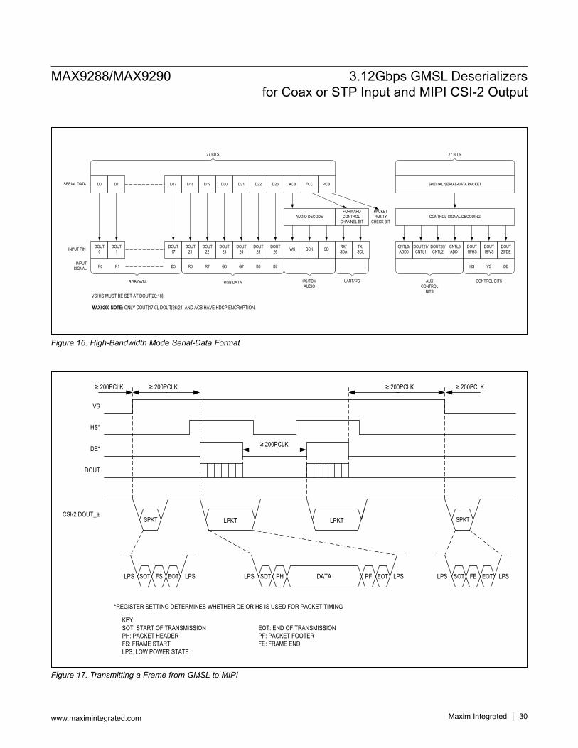
MAX9288/MAX9290 3.12Gbps GMSL Deserializers for Coax or STP Input and MIPI CSI-2 Output
www.maximintegrated.com Maxim Integrated 30
Figure 16. High-Bandwidth Mode Serial-Data Format
Figure 17. Transmitting a Frame from GMSL to MIPI
D0SERIAL DATA D1
27 BITS
INPUT PIN DOUT0
DOUT1
D17 D18 D19 D20 D21 D22 D23 ACB FCC PCB
DOUT17
DOUT21
DOUT22
DOUT23
DOUT24
DOUT25
DOUT26 WS SCK SD RX/
SDATX/SCL
INPUTSIGNAL R0 R1 B5 R6 R7 G6 G7 B6 B7 HS VS DE
RGB DATA RGB DATA I2S/TDMAUDIO
UART/I2C
VS/HS MUST BE SET AT DOUT[20:18].
MAX9290 NOTE: ONLY DOUT[17:0], DOUT[26:21] AND ACB HAVE HDCP ENCRYPTION.
AUDIO DECODEFORWARDCONTROL-
CHANNEL BIT
PACKETPARITY
CHECK BIT
SPECIAL SERIAL-DATA PACKET
CNTL0/ADD0
DOUT27/CNTL1
DOUT28/CNTL2
CNTL3ADD1
DOUT18/HS
DOUT19/VS
DOUT20/DE
AUXCONTROL
BITS
CONTROL BITS
CONTROL-SIGNAL DECODING
27 BITS
VS
DE*
DOUT
CSI-2 DOUT_±
HS*
KEY:SOT: START OF TRANSMISSION EOT: END OF TRANSMISSIONPH: PACKET HEADER PF: PACKET FOOTERFS: FRAME START FE: FRAME ENDLPS: LOW POWER STATE
SOT FS EOTLPS LPS SOT FE EOTLPS LPS
LPKTSPKT LPKT SPKT
SOT PH EOTLPS LPSDATA PF
*REGISTER SETTING DETERMINES WHETHER DE OR HS IS USED FOR PACKET TIMING
≥ 200PCLK ≥ 200PCLK
≥ 200PCLK
≥ 200PCLK≥ 200PCLK
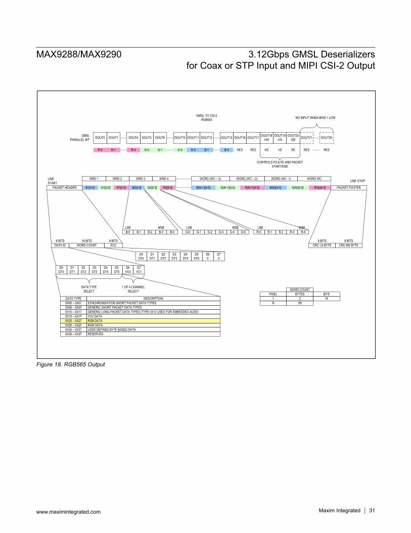
MAX9288/MAX9290 3.12Gbps GMSL Deserializers for Coax or STP Input and MIPI CSI-2 Output
www.maximintegrated.com Maxim Integrated 31
Figure 18. RGB565 Output
VS DE
DOUT0 DOUT1 DOUT18/HS
DOUT19/VS
DOUT20/DE DOUT21 DOUT26GMSL
PARALLEL BIT
R-0 R-1 R-4
DOUT4 DOUT5 DOUT6 DOUT10 DOUT11 DOUT12 DOUT15
G-0 G-1 G-5 B-0 B-1 B-4
GMSL TO CSI-2RGB565
B2[4:0]PACKET HEADER R2[4:0] B(N-1)[4:0] R(N-1)[4:0] B(N)[4:0] R(N)[4:0]G(N)[5:0] PACKET FOOTER
DATA ID WORD COUNT ECC
B-0 B-1 B-2 B-3 B-4 G-0 G-1 G-2 R-0 R-1 R-2 R-3 R-4G-3 G-4 G-5
8 BITS 16 BITS 8 BITS
D70
D60
D5DT5
D4DT4
D3DT3
D2DT2
D1DT1
D0DT0
D7VC1
D6VC0
D5DT5
D4DT4
D3DT3
D2DT2
D1DT1
D0DT0
CRC LS BYTE CRC MS BYTE
DATA TYPE0X00 – 0X070X08 – 0X0F0X10 – 0X170X18 – 0X1F
0X30 – 0X370X38 – 0X3F
0X20 – 0X270X28 – 0X2F
DESCRIPTIONSYNCHRONIZATION SHORT PACKET DATA TYPESGENERIC SHORT PACKET DATA TYPESGENERIC LONG PACKET DATA TYPES (TYPE 0X12 USED FOR EMBEDDED AUDIOYUV DATA
USER DEFINED BYTE BASED DATARESERVED
RGB DATARAW DATA
1 OF 4 CHANNEL SELECT
DATA TYPE SELECT
8 BITS 8 BITS
WORD COUNTPIXEL BYTES BITS
1 2 16
LINE START LINE STOP
RES RES
DOUT16 DOUT17
RES RES
NO INPUT WHEN BWS = LOW
B1[4:0] R1[4:0]
N 2N
CONTROLS FS & FE AND PACKET START/END
G(N-1)[5:0]G2[5:0]G1[5:0]
WRD 1 WRD 2 WRD 3 WRD 4 WORD (WC – 2) WORD (WC -1) WORD WCWORD (WC – 3)
MSBLSB MSBLSB MSBLSB
HS
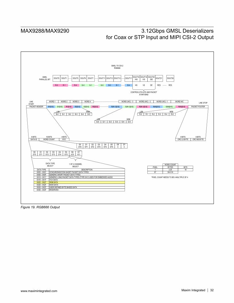
MAX9288/MAX9290 3.12Gbps GMSL Deserializers for Coax or STP Input and MIPI CSI-2 Output
www.maximintegrated.com Maxim Integrated 32
Figure 19. RGB666 Output
CONTROLS FS & FE AND PACKET START/END
DOUT0 DOUT1 DOUT18/HS
DOUT19/VS
DOUT20/DE DOUT21 DOUT26GMSL
PARALLEL BIT DOUT5 DOUT6 DOUT7 DOUT11 DOUT12 DOUT13 DOUT17
GMSL TO CSI-2RGB666
B2[5:0]PACKET HEADER R2[5:0]G2[5:0]B1[5:0] R1[5:0]G1[5:0] B(N-1)[5:0] R(N-1)[5:0]G(N-1)[5:0] B(N)[5:0] R(N)[5:0]G(N)[5:0] PACKET FOOTER
DATA ID WORD COUNT ECC
B-0 B-1 B-2 B-3 B-4 B-5
G-0 G-1 G-2 G-3 G-4 G-5
R-0 R-1 R-2 R-3 R-4 R-5
8 BITS 16 BITS 8 BITS
D70
D60
D5DT5
D4DT4
D3DT3
D2DT2
D1DT1
D0DT0
D7VC1
D6VC0
D5DT5
D4DT4
D3DT3
D2DT2
D1DT1
D0DT0
CRC LS BYTE CRC MS BYTE
DATA TYPE0X00 – 0X070X08 – 0X0F0X10 – 0X170X18 – 0X1F
0X30 – 0X370X38 – 0X3F
0X20 – 0X270X28 – 0X2F
DESCRIPTIONSYNCHRONIZATION SHORT PACKET DATA TYPESGENERIC SHORT PACKET DATA TYPESGENERIC LONG PACKET DATA TYPES (TYPE 0X12 USED FOR EMBEDDED AUDIOYUV DATA
USER DEFINED BYTE BASED DATARESERVED
RGB DATARAW DATA
1 OF 4 CHANNEL SELECT
DATA TYPE SELECT
8 BITS 8 BITS
WORD COUNTPIXEL BYTES BITS
1 2.25 18
LINE START LINE STOP
HS VS DER-0 R-1 R-4 G-0 G-1 G-5 B-0 B-1 B-4 RES RES
*PIXEL COUNT NEEDS TO BE A MULTIPLE OF 4
WORD 1 WORD 2 WORD 3 WORD 4 WORD (WC) - 2 WORD (WC) -1 WORD WCWORD (WC) - 3
N* 9/4 X N
MSBLSB
MSBLSB
MSBLSB
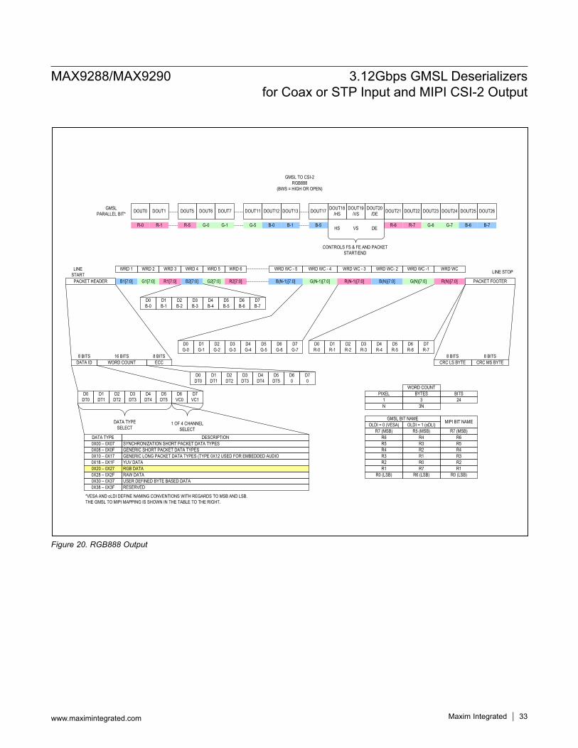
MAX9288/MAX9290 3.12Gbps GMSL Deserializers for Coax or STP Input and MIPI CSI-2 Output
www.maximintegrated.com Maxim Integrated 33
Figure 20. RGB888 Output
HS VS DE
CONTROLS FS & FE AND PACKET START/END
DOUT0 DOUT1 DOUT18/HS
DOUT19/VS
DOUT20/DE DOUT21 DOUT22 DOUT23 DOUT24 DOUT25 DOUT26GMSL
PARALLEL BIT*
R-0 R-1 R-5
DOUT5 DOUT6 DOUT7 DOUT11 DOUT12 DOUT13 DOUT17
G-0 G-1 G-5 B-0 B-1 B-5 R-6 R-7 G-6 G-7 B-6 B-7
GMSL TO CSI-2RGB888
(BWS = HIGH OR OPEN)
B1[7:0]PACKET HEADER R1[7:0]G1[7:0] B2[7:0] R2[7:0]G2[7:0] B(N-1)[7:0] R(N-1)[7:0]G(N-1)[7:0] B(N)[7:0] R(N)[7:0]G(N)[7:0] PACKET FOOTER
DATA ID WORD COUNT ECC
D0 B-0
D1 B-1
D2 B-2
D3 B-3
D4 B-4
D5 B-5
D6 B-6
D7 B-7
8 BITS 16 BITS 8 BITS
D70
D60
D5DT5
D4DT4
D3DT3
D2DT2
D1DT1
D0DT0
D7VC1
D6VC0
D5DT5
D4DT4
D3DT3
D2DT2
D1DT1
D0DT0
CRC LS BYTE CRC MS BYTE
DATA TYPE0X00 – 0X070X08 – 0X0F0X10 – 0X170X18 – 0X1F
0X30 – 0X370X38 – 0X3F
0X20 – 0X270X28 – 0X2F
DESCRIPTIONSYNCHRONIZATION SHORT PACKET DATA TYPESGENERIC SHORT PACKET DATA TYPESGENERIC LONG PACKET DATA TYPES (TYPE 0X12 USED FOR EMBEDDED AUDIOYUV DATA
USER DEFINED BYTE BASED DATARESERVED
RGB DATARAW DATA
1 OF 4 CHANNEL SELECT
DATA TYPE SELECT
8 BITS 8 BITS
LINE START LINE STOPWRD 1 WRD 2 WRD 3 WRD 4 WRD WC- 2 WRD WC -1 WRD WCWRD WC - 4WRD 5 WRD 6 WRD WC - 5 WRD WC - 3
D0 G-0
D1 G-1
D2 G-2
D3 G-3
D4 G-4
D5 G-5
D6G-6
D7 G-7
D0 R-0
D1 R-1
D2 R-2
D3 R-3
D4 R-4
D5 R-5
D6 R-6
D7 R-7
*VESA AND oLDI DEFINE NAMING CONVENTIONS WITH REGARDS TO MSB AND LSB.THE GMSL TO MIPI MAPPING IS SHOWN IN THE TABLE TO THE RIGHT.
WORD COUNTPIXEL BYTES BITS
1 3 24N 3N
OLDI = 0 (VESA)R7 (MSB)
R6R5
OLDI = 1 (oDLI)
R4R3R2R1
R0 (LSB)R7
R4R5 (MSB)
R3R2R1
R6 (LSB)
R0
GMSL BIT NAME MIPI BIT NAME
R1
R7 (MSB)
R5R4R3
R0 (LSB)
R2
R6
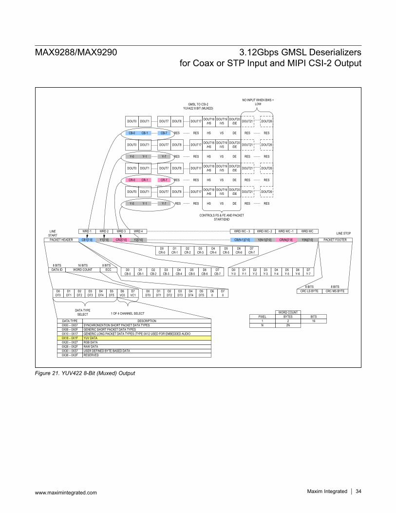
MAX9288/MAX9290 3.12Gbps GMSL Deserializers for Coax or STP Input and MIPI CSI-2 Output
www.maximintegrated.com Maxim Integrated 34
Figure 21. YUV422 8-Bit (Muxed) Output
DOUT0 DOUT1
CB-0 CB-1 CB-7
DOUT7 DOUT8
GMSL TO CSI-2YUV422 8 BIT (MUXED)
Y2[7:0]PACKET HEADER CB1[7:0] CR2[7:0]Y1[7:0] CB(N-1)[7:0] Y(N-1)[7:0] Y(N)[7:0]CR(N)[7:0] PACKET FOOTER
DATA ID WORD COUNT ECC8 BITS 16 BITS 8 BITS
D70
D60
D5DT5
D4DT4
D3DT3
D2DT2
D1DT1
D0DT0
D7VC1
D6VC0
D5DT5
D4DT4
D3DT3
D2DT2
D1DT1
D0DT0
CRC LS BYTE CRC MS BYTE
DATA TYPE0X00 – 0X070X08 – 0X0F0X10 – 0X170X18 – 0X1F
0X30 – 0X370X38 – 0X3F
0X20 – 0X270X28 – 0X2F
DESCRIPTIONSYNCHRONIZATION SHORT PACKET DATA TYPESGENERIC SHORT PACKET DATA TYPESGENERIC LONG PACKET DATA TYPES (TYPE 0X12 USED FOR EMBEDDED AUDIOYUV DATA
USER DEFINED BYTE BASED DATARESERVED
RGB DATARAW DATA
1 OF 4 CHANNEL SELECTDATA TYPE
SELECT
8 BITS 8 BITS
WORD COUNTPIXEL BYTES BITS
1 2 16
LINE START LINE STOP
N 2N
WRD WC- 2 WRD WC -1 WRD WCWRD WC - 3
HS VS DE
DOUT18/HS
DOUT19/VS
DOUT20/DE DOUT21 DOUT26
RES RES
DOUT17
RES
NO INPUT WHEN BWS = LOW
DOUT0 DOUT1
CR-0 CR-1 CR-7
DOUT7 DOUT8
HS VS DE
DOUT18/HS
DOUT19/VS
DOUT20/DE DOUT21 DOUT26
RES RES
DOUT17
RES
CONTROLS FS & FE AND PACKET START/END
DOUT0 DOUT1 DOUT7 DOUT8
HS VS DE
DOUT18/HS
DOUT19/VS
DOUT20/DE DOUT21 DOUT26
RES RES
DOUT17
RES
DOUT0 DOUT1 DOUT7 DOUT8
Y-0 Y-1 Y-7
HS VS DE
DOUT18/HS
DOUT19/VS
DOUT20/DE DOUT21 DOUT26
RES RES
DOUT17
RES
Y-0 Y-1 Y-7
RES
RES
RES
RES
D7 CB-7
D6 CB-6
D5 CB-5
D4 CB-4
D3 CB-3
D2 CB-2
D1 CB-1
D0 CB-0
D7 Y-7
D6 Y-6
D5 Y-5
D4 Y-4
D3 Y-3
D2 Y-2
D1 Y-1
D0 Y-0
D7 CR-7
D6 CR-6
D5 CR-5
D4 CR-4
D3 CR-3
D2 CR-2
D1 CR-1
D0 CR-0
WRD 1 WRD 2 WRD 3 WRD 4
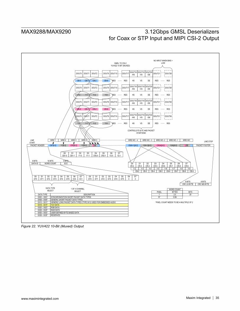
MAX9288/MAX9290 3.12Gbps GMSL Deserializers for Coax or STP Input and MIPI CSI-2 Output
www.maximintegrated.com Maxim Integrated 35
Figure 22. YUV422 10-Bit (Muxed) Output
DOUT0 DOUT1
CB-0 CB-1 CB-2
DOUT2 DOUT10
GMSL TO CSI-2YUV422 10 BIT (MUXED)
Y2[9:2]PACKET HEADER CB1[9:2] CR2[9:2]Y1[9:2] CB(N-1)[9:2] Y(N-1)[9:2] Y(N)[9:2]CR(N)[9:2] PACKET FOOTER
DATA ID WORD COUNT ECC8 BITS 16 BITS 8 BITS
D70
D60
D5DT5
D4DT4
D3DT3
D2DT2
D1DT1
D0DT0
D7VC1
D6VC0
D5DT5
D4DT4
D3DT3
D2DT2
D1DT1
D0DT0
CRC LS BYTE CRC MS BYTE
DATA TYPE0X00 – 0X070X08 – 0X0F0X10 – 0X170X18 – 0X1F
0X30 – 0X370X38 – 0X3F
0X20 – 0X270X28 – 0X2F
DESCRIPTIONSYNCHRONIZATION SHORT PACKET DATA TYPESGENERIC SHORT PACKET DATA TYPESGENERIC LONG PACKET DATA TYPES (TYPE 0X12 USED FOR EMBEDDED AUDIOYUV DATA
USER DEFINED BYTE BASED DATARESERVED
RGB DATARAW DATA
1 OF 4 CHANNEL SELECT
DATA TYPE SELECT
8 BITS 8 BITS
WORD COUNTPIXEL BYTES BITS
1 2.5 20
LINE START LINE STOP
N* 2.5N
WRD WC- 2 WRD WC -1 WRD WCWRD WC - 3
HS VS DE
DOUT18/HS
DOUT19/VS
DOUT20/DE DOUT21 DOUT26
RES RES
DOUT17
RES
NO INPUT WHEN BWS = LOW
DOUT0 DOUT1
CR-0 CR-1 CR-2
DOUT2 DOUT10
HS VS DE
DOUT18/HS
DOUT19/VS
DOUT20/DE DOUT21 DOUT26
RES RES
DOUT17
RES
CONTROLS FS & FE AND PACKET START/END
DOUT2 DOUT10
HS VS DE
DOUT18/HS
DOUT19/VS
DOUT20/DE DOUT21 DOUT26
RES RES
DOUT17
RES
DOUT2 DOUT10
Y-0 Y-1 Y-2
HS VS DE
DOUT18/HS
DOUT19/VS
DOUT20/DE DOUT21 DOUT26
RES RES
DOUT17
RES
Y-2
RES
RES
RES
RES
DOUT9
CB-9
DOUT9
CR-9
DOUT9
DOUT9
Y-9
Y-9
LSB LSB
WRD WC - 4
*PIXEL COUNT NEEDS TO BE A MULTIPLE OF 2
Y-8 Y-9Y-2 Y-3 Y-4 Y-5 Y-6 Y-7
D6 CR-8
D7 CR-9
D0 CR-2
D1 CR-3
D2 CR-4
D3 CR-5
D4 CR-6
D5 CR-7
CB-8 CB-9CB-2 CB-3 CB-4 CB-5 CB-6 CB-7
D6 Y2-0
D7 Y2-1
D4 CR2-0
D5 CR2-1
D2 Y1-0
D3 Y1-1
D0 CB1-0
D1 CB1-1
Y-0 Y-1
WRD 1 WRD 2 WRD 3 WRD 4 WRD 5
DOUT0 DOUT1
DOUT0 DOUT1
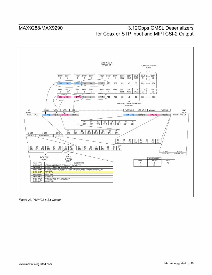
MAX9288/MAX9290 3.12Gbps GMSL Deserializers for Coax or STP Input and MIPI CSI-2 Output
www.maximintegrated.com Maxim Integrated 36
Figure 23. YUV422 8-Bit Output
DOUT0
DOUT1
CB-0 CB-1 CB-7
DOUT7
DOUT8
DOUT9
DOUT15
Y-0 Y-1 Y-7
GMSL TO CSI-2YUV422 8 BIT
Y2[7:0]PACKET HEADER CB1[7:0] CR2[7:0]Y1[7:0] CB(N-1)[7:0] Y(N-1)[7:0] Y(N)[7:0]CR(N)[7:0] PACKET FOOTER
DATA ID WORD COUNT ECC8 BITS 16 BITS 8 BITS
D70
D60
D5DT5
D4DT4
D3DT3
D2DT2
D1DT1
D0DT0
D7VC1
D6VC0
D5DT5
D4DT4
D3DT3
D2DT2
D1DT1
D0DT0
CRC LS BYTE CRC MS BYTE
DATA TYPE0X00 – 0X070X08 – 0X0F0X10 – 0X170X18 – 0X1F
0X30 – 0X370X38 – 0X3F
0X20 – 0X270X28 – 0X2F
DESCRIPTIONSYNCHRONIZATION SHORT PACKET DATA TYPESGENERIC SHORT PACKET DATA TYPESGENERIC LONG PACKET DATA TYPES (TYPE 0X12 USED FOR EMBEDDED AUDIOYUV DATA
USER DEFINED BYTE BASED DATARESERVED
RGB DATARAW DATA
1 OF 4 CHANNEL SELECT
DATA TYPE SELECT
8 BITS 8 BITS
WORD COUNTPIXEL BYTES BITS
1 2 16
LINE START
LINE STOP
N 2N
WRD WC- 2 WRD WC -1 WRD WCWRD WC - 3
HS VS DE
DOUT18/HS
DOUT19/VS
DOUT20/DE
DOUT21
DOUT26
RES RES
DOUT16
DOUT17
RES RES
NO INPUT WHEN BWS = LOW
DOUT0
DOUT1
CR-0 CR-1 CR-7
DOUT7
DOUT8
DOUT9
DOUT15
Y-0 Y-1 Y-7 HS VS DE
DOUT18/HS
DOUT19/VS
DOUT20/DE
DOUT21
DOUT26
RES RES
DOUT16
DOUT17
RES RES
CONTROLS FS & FE AND PACKET START/END
D7 CB-7
D6 CB-6
D5 CB-5
D4 CB-4
D3 CB-3
D2 CB-2
D1 CB-1
D0 CB-0
D7 CR-7
D6 CR-6
D5 CR-5
D4 CR-4
D3 CR-3
D2 CR-2
D1 CR-1
D0 CR-0
D7 Y-7
D6 Y-6
D5 Y-5
D4 Y-4
D3 Y-3
D2 Y-2
D1 Y-1
D0 Y-0
WRD 1 WRD 2 WRD 3 WRD 4
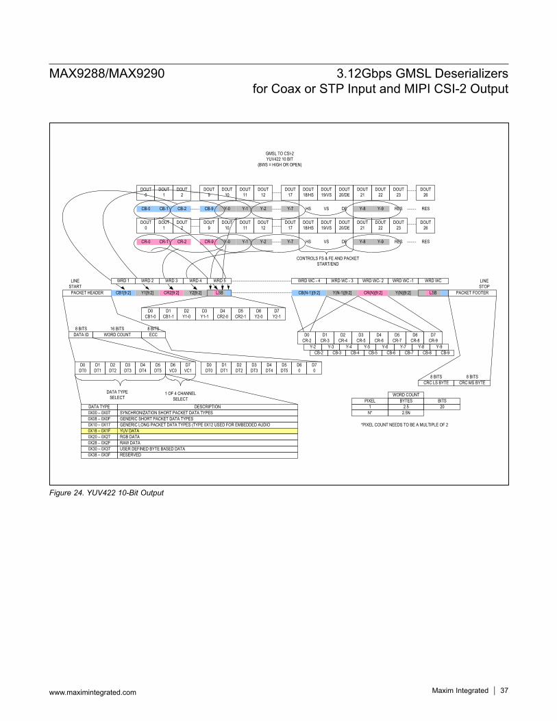
MAX9288/MAX9290 3.12Gbps GMSL Deserializers for Coax or STP Input and MIPI CSI-2 Output
www.maximintegrated.com Maxim Integrated 37
Figure 24. YUV422 10-Bit Output
DOUT0
DOUT1
CB-0 CB-1 CB-2
DOUT2
GMSL TO CSI-2YUV422 10 BIT
(BWS = HIGH OR OPEN)
Y2[9:2]PACKET HEADER CB1[9:2] CR2[9:2]Y1[9:2] CB(N-1)[9:2] Y(N-1)[9:2] Y(N)[9:2]CR(N)[9:2] PACKET FOOTER
DATA ID WORD COUNT ECC
D6 Y2-0
D7 Y2-1
D4 CR2-0
D5 CR2-1
D2 Y1-0
D3 Y1-1
D0 CB1-0
D1 CB1-1
8 BITS 16 BITS 8 BITS
D70
D60
D5DT5
D4DT4
D3DT3
D2DT2
D1DT1
D0DT0
D7VC1
D6VC0
D5DT5
D4DT4
D3DT3
D2DT2
D1DT1
D0DT0
CRC LS BYTE CRC MS BYTE
DATA TYPE0X00 – 0X070X08 – 0X0F0X10 – 0X170X18 – 0X1F
0X30 – 0X370X38 – 0X3F
0X20 – 0X270X28 – 0X2F
DESCRIPTIONSYNCHRONIZATION SHORT PACKET DATA TYPESGENERIC SHORT PACKET DATA TYPESGENERIC LONG PACKET DATA TYPES (TYPE 0X12 USED FOR EMBEDDED AUDIOYUV DATA
USER DEFINED BYTE BASED DATARESERVED
RGB DATARAW DATA
1 OF 4 CHANNEL SELECT
DATA TYPE SELECT
8 BITS 8 BITS
WORD COUNTPIXEL BYTES BITS
1 2.5 20
LINE START
LINE STOP
N* 2.5N
WRD WC- 2 WRD WC -1 WRD WCWRD WC - 3
HS VS DE
DOUT18/HS
DOUT19/VS
DOUT20/DE
DOUT23
DOUT26
RES RES
CR-0 CR-1 CR-2
CONTROLS FS & FE AND PACKET START/END
DOUT10
DOUT11
DOUT12
HS VS DE
DOUT18/HS
DOUT19/VS
DOUT20/DE
DOUT0
DOUT1
DOUT2
Y-0 Y-1 Y-2
DOUT9
CB-9
CR-9
DOUT17
DOUT9
Y-7
LSB LSB
WRD WC - 4
*PIXEL COUNT NEEDS TO BE A MULTIPLE OF 2
DOUT21
Y-8
DOUT22
Y-9
Y-0 Y-1 Y-2 Y-7
DOUT10
DOUT11
DOUT12
DOUT17
DOUT23
DOUT26
RES RES
DOUT21
Y-8
DOUT22
Y-9
Y-8 Y-9Y-2 Y-3 Y-4 Y-5 Y-6 Y-7
D6 CR-8
D7 CR-9
D0 CR-2
D1 CR-3
D2 CR-4
D3 CR-5
D4 CR-6
D5 CR-7
CB-8 CB-9CB-2 CB-3 CB-4 CB-5 CB-6 CB-7
WRD 1 WRD 2 WRD 3 WRD 4 WRD 5
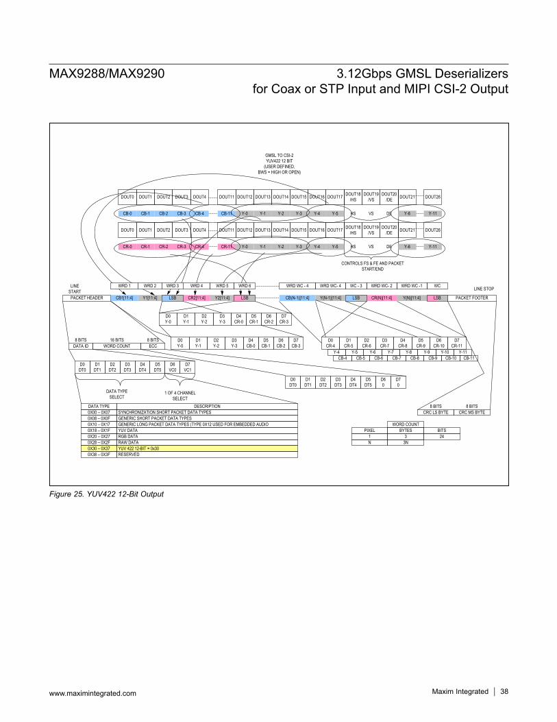
MAX9288/MAX9290 3.12Gbps GMSL Deserializers for Coax or STP Input and MIPI CSI-2 Output
www.maximintegrated.com Maxim Integrated 38
Figure 25. YUV422 12-Bit Output
DOUT0 DOUT1
CB-0 CB-1 CB-2
DOUT2
GMSL TO CSI-2YUV422 12 BIT
(USER DEFINED, BWS = HIGH OR OPEN)
Y2[11:4]PACKET HEADER CB1[11:4] CR2[11:4]Y1[11:4] CB(N-1)[11:4] Y(N-1)[11:4] Y(N)[11:4]CR(N)[11:4] PACKET FOOTER
DATA ID WORD COUNT ECCD7
CB-3D6
CB-2D3 Y-3
D2 Y-2
8 BITS 16 BITS 8 BITS
D70
D60
D5DT5
D4DT4
D3DT3
D2DT2
D1DT1
D0DT0
D7VC1
D6VC0
D5DT5
D4DT4
D3DT3
D2DT2
D1DT1
D0DT0
CRC LS BYTE CRC MS BYTEDATA TYPE0X00 – 0X070X08 – 0X0F0X10 – 0X170X18 – 0X1F
0X30 – 0X370X38 – 0X3F
0X20 – 0X270X28 – 0X2F
DESCRIPTIONSYNCHRONIZATION SHORT PACKET DATA TYPESGENERIC SHORT PACKET DATA TYPESGENERIC LONG PACKET DATA TYPES (TYPE 0X12 USED FOR EMBEDDED AUDIOYUV DATA
YUV 422 12-BIT = 0x30RESERVED
RGB DATARAW DATA
1 OF 4 CHANNEL SELECT
DATA TYPE SELECT
8 BITS 8 BITS
WORD COUNTPIXEL BYTES BITS
1 3 24
LINE START LINE STOP
N 3N
WRD WC- 2 WRD WC -1 WCWC - 3
CB-8 CB-9 CB-10 CB-11CB-4 CB-5 CB-6 CB-7
HS VS DE
DOUT18/HS
DOUT19/VS
DOUT20/DE DOUT26
CONTROLS FS & FE AND PACKET START/END
DOUT12 DOUT13 DOUT14
Y-0 Y-1 Y-2
DOUT11
CB-11
DOUT17
Y-5
LSB
WRD WC- 4
DOUT21
Y-6
DOUT3
CB-3 CB-4
DOUT4 DOUT15 DOUT16
Y-3 Y-4 Y-11
DOUT0 DOUT1
CR-0 CR-1 CR-2
DOUT2
HS VS DE
DOUT18/HS
DOUT19/VS
DOUT20/DE DOUT26DOUT12 DOUT13 DOUT14
Y-0 Y-1 Y-2
DOUT11
CR-11
DOUT17
Y-5
DOUT21
Y-6
DOUT3
CR-3 CR-4
DOUT4 DOUT15 DOUT16
Y-3 Y-4 Y-11
LSB LSB LSB
WRD WC - 4
D5 CB-1
D4 CB-0
D1 Y-1
D0 Y-0
Y-8 Y-9 Y-10 Y-11Y-4 Y-5 Y-6 Y-7
D4 CR-8
D5 CR-9
D6 CR-10
D7 CR-11
D0 CR-4
D1 CR-5
D2 CR-6
D3 CR-7
D7 CR-3
D6 CR-2
D3 Y-3
D2 Y-2
D5 CR-1
D4 CR-0
D1 Y-1
D0 Y-0
WRD 1 WRD 2 WRD 3 WRD 4 WRD 5 WRD 6
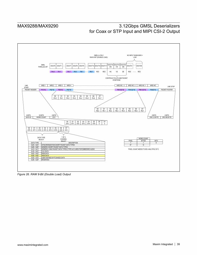
MAX9288/MAX9290 3.12Gbps GMSL Deserializers for Coax or STP Input and MIPI CSI-2 Output
www.maximintegrated.com Maxim Integrated 39
Figure 26. RAW 8-Bit (Double Load) Output
HS VS DE
CONTROLS FS & FE AND PACKET START/END
DOUT0 DOUT1 DOUT18/HS
DOUT19/VS
DOUT20/DE
GMSLPARALLEL BIT
PA-0 PA-1 PA-7
DOUT7 DOUT8 DOUT9 DOUT15 DOUT16 DOUT17
PB-0 PB-1 PB-7
GMSL to CSI-2RAW 8 BIT (DOUBLE LOAD)
PACKET HEADER P1[7:0] P2[7:0] P(N-3)[7:0] P(N-2)[7:0] P(N)[7:0]P(N-1)[7:0] PACKET FOOTER
DATA ID WORD COUNT ECC8 BITS 16 BITS 8 BITS
D70
D60
D5DT5
D4DT4
D3DT3
D2DT2
D1DT1
D0DT0
D7VC1
D6VC0
D5DT5
D4DT4
D3DT3
D2DT2
D1DT1
D0DT0
CRC LS BYTE CRC MS BYTE
DATA TYPE0x00 – 0x070x08 – 0x0F0x10 – 0x170x18 – 0x1F
0x30 – 0x370x38 – 0x3F
0x20 – 0x270x28 – 0x2F
DESCRIPTIONSYNCHRONIZATION SHORT PACKET DATA TYPESGENERIC SHORT PACKET DATA TYPESGENERIC LONG PACKET DATA TYPES (TYPE 0x12 USED FOR EMBEDDED AUDIOYUV DATA
USER DEFINED BYTE BASED DATARESERVED
RGB DATARAW DATA
1 OF 4 CHANNEL SELECT
DATA TYPE SELECT
8 BITS 8 BITS
WORD COUNTPIXEL BYTES BITS
1 1 8
LINE START LINE STOP
N* N
WRD 1 WRD 2 WRD 3 WRD 4 WRD WC- 2 WRD WC -1 WRD WCWRD WC - 3
DOUT21 DOUT26
RES RES
NO INPUT WHEN BWS = LOW
RESRES
P3[7:0] P4[7:0]
*PIXEL COUNT NEEDS TO BE A MULTIPLE OF 2
D7 PA-7
D6 PA-6
D5 PA-5
D4 PA-4
D3 PA-3
D2 PA-2
D1 PA-1
D0 PA-0
D7 PB-7
D6 PB-6
D5 PB-5
D4 PB-4
D3 PB-3
D2 PB-2
D1 PB-1
D0 PB-0
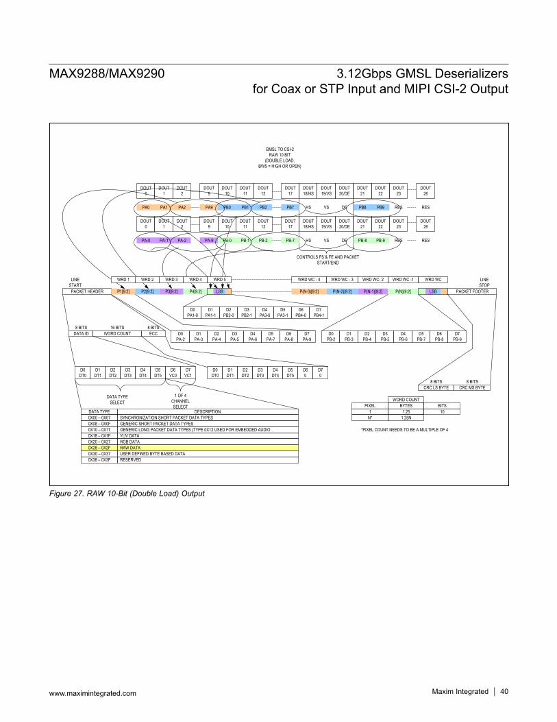
MAX9288/MAX9290 3.12Gbps GMSL Deserializers for Coax or STP Input and MIPI CSI-2 Output
www.maximintegrated.com Maxim Integrated 40
Figure 27. RAW 10-Bit (Double Load) Output
DOUT0
DOUT1
PA0 PA1 PA2
DOUT2
GMSL TO CSI-2RAW 10 BIT
(DOUBLE LOAD,BWS = HIGH OR OPEN)
P4[9:2]PACKET HEADER P1[9:2] P3[9:2]P2[9:2] P(N-3)[9:2] P(N-2)[9:2] P(N)[9:2]P(N-1)[9:2] PACKET FOOTER
DATA ID WORD COUNT ECC
D6 PB4-0
D7 PB4-1
D4 PA3-0
D5 PA3-1
D2 PB2-0
D3 PB2-1
D0 PA1-0
D1 PA1-1
8 BITS 16 BITS 8 BITS
D70
D60
D5DT5
D4DT4
D3DT3
D2DT2
D1DT1
D0DT0
D7VC1
D6VC0
D5DT5
D4DT4
D3DT3
D2DT2
D1DT1
D0DT0
CRC LS BYTE CRC MS BYTE1 OF 4
CHANNEL SELECT
DATA TYPE SELECT
8 BITS 8 BITS
LINE START
LINE STOP
WRD WC- 2 WRD WC -1 WRD WCWRD WC - 3
HS VS DE
DOUT18/HS
DOUT19/VS
DOUT20/DE
DOUT23
DOUT26
RES RES
PA-0 PA-1 PA-2
CONTROLS FS & FE AND PACKET START/END
DOUT10
DOUT11
DOUT12
HS VS DE
DOUT18/HS
DOUT19/VS
DOUT20/DE
DOUT0
DOUT1
DOUT2
PB0 PB1 PB2
DOUT9
PA9
PA-9
DOUT17
DOUT9
PB7
LSB LSB
WRD WC - 4
DOUT21
PB8
DOUT22
PB9
PB-0 PB-1 PB-2 PB-7
DOUT10
DOUT11
DOUT12
DOUT17
DOUT23
DOUT26
RES RES
DOUT21
PB-8
DOUT22
PB-9
DATA TYPE0X00 – 0X070X08 – 0X0F0X10 – 0X170X18 – 0X1F
0X30 – 0X370X38 – 0X3F
0X20 – 0X270X28 – 0X2F
DESCRIPTIONSYNCHRONIZATION SHORT PACKET DATA TYPESGENERIC SHORT PACKET DATA TYPESGENERIC LONG PACKET DATA TYPES (TYPE 0X12 USED FOR EMBEDDED AUDIOYUV DATA
USER DEFINED BYTE BASED DATARESERVED
RGB DATARAW DATA
WORD COUNTPIXEL BYTES BITS
1 1.25 10N* 1.25N
*PIXEL COUNT NEEDS TO BE A MULTIPLE OF 4
D6 PB-8
D7PB-9
D0 PB-2
D1 PB-3
D2 PB-4
D3 PB-5
D4 PB-6
D5 PB-7
D6 PA-8
D7 PA-9
D0 PA-2
D1 PA-3
D2 PA-4
D3 PA-5
D4 PA-6
D5 PA-7
WRD 1 WRD 2 WRD 3 WRD 4 WRD 5
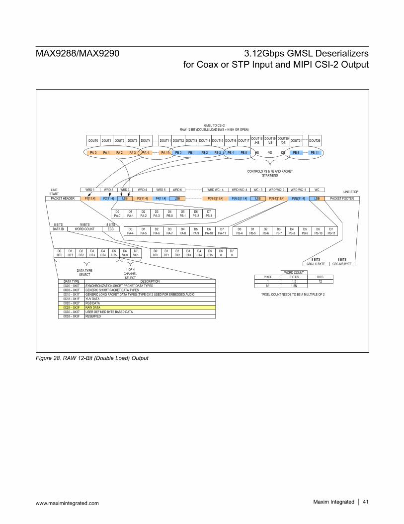
MAX9288/MAX9290 3.12Gbps GMSL Deserializers for Coax or STP Input and MIPI CSI-2 Output
www.maximintegrated.com Maxim Integrated 41
Figure 28. RAW 12-Bit (Double Load) Output
DOUT0 DOUT1
PA-0 PA-1 PA-2
DOUT2
GMSL TO CSI-2RAW 12 BIT (DOUBLE LOAD BWS = HIGH OR OPEN)
P4[11:4]PACKET HEADER P1[11:4] P3[11:4]P2[11:4] P(N-3)[11:4] P(N-2)[11:4] P(N)[11:4]P(N-1)[11:4] PACKET FOOTER
DATA ID WORD COUNT ECC8 BITS 16 BITS 8 BITS
D70
D60
D5DT5
D4DT4
D3DT3
D2DT2
D1DT1
D0DT0
D7VC1
D6VC0
D5DT5
D4DT4
D3DT3
D2DT2
D1DT1
D0DT0
CRC LS BYTE CRC MS BYTE
DATA TYPE0X00 – 0X070X08 – 0X0F0X10 – 0X170X18 – 0X1F
0X30 – 0X370X38 – 0X3F
0X20 – 0X270X28 – 0X2F
DESCRIPTIONSYNCHRONIZATION SHORT PACKET DATA TYPESGENERIC SHORT PACKET DATA TYPESGENERIC LONG PACKET DATA TYPES (TYPE 0X12 USED FOR EMBEDDED AUDIOYUV DATA
USER DEFINED BYTE BASED DATARESERVED
RGB DATARAW DATA
1 OF 4 CHANNEL SELECT
DATA TYPE SELECT
8 BITS 8 BITS
WORD COUNTPIXEL BYTES BITS
1 1.5 12
LINE START LINE STOP
N* 1.5N
WRD 4 WRD WC- 2 WRD WC -1 WCWC - 3
CONTROLS FS & FE AND PACKET START/END
DOUT11
PA-11
WRD 5
LSB
WRD WC- 4
*PIXEL COUNT NEEDS TO BE A MULTIPLE OF 2
DOUT3
PA-3 PA-4
DOUT4
LSB LSB LSB
WRD 6 WRD WC - 4
HS VS DE
DOUT18/HS
DOUT19/VS
DOUT20/DE DOUT26DOUT12 DOUT13 DOUT14
PB-0 PB-1 PB-2
DOUT17
PB-5
DOUT21
PB-6
DOUT15 DOUT16
PB-3 PB-4 PB-11
D3 PA-7
D2 PA-6
D1 PA-5
D0 PA-4
D7 PA-11
D6 PA-10
D5 PA-9
D4 PA-8
D7 PB-3
D6 PB-2
D3 PA-3
D2 PA-2
D5 PB-1
D4 PB-0
D1 PA-1
D0 PA-0
D3 PB-7
D2 PB-6
D1 PB-5
D0 PB-4
D7 PB-11
D6 PB-10
D5 PB-9
D4 PB-8
WRD 1 WRD 2 WRD 3
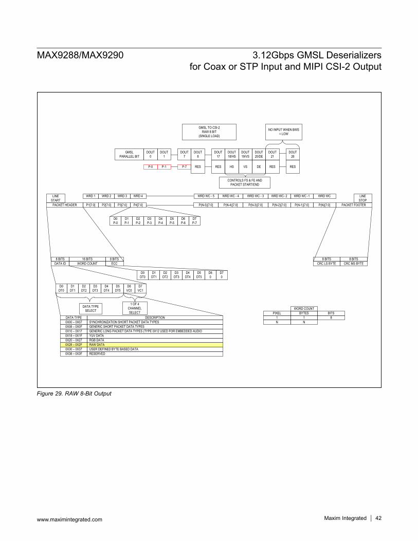
MAX9288/MAX9290 3.12Gbps GMSL Deserializers for Coax or STP Input and MIPI CSI-2 Output
www.maximintegrated.com Maxim Integrated 42
Figure 29. RAW 8-Bit Output
DOUT0
DOUT1
GMSLPARALLEL BIT
P-0 P-1 P-7
DOUT7
DOUT8
GMSL TO CSI-2RAW 8 BIT
(SINGLE LOAD)
P4[7:0]PACKET HEADER P1[7:0] P3[7:0]P2[7:0] P(N-5)[7:0] P(N-3)[7:0]P(N-4)[7:0] P(N-2)[7:0] P(N)[7:0]P(N-1)[7:0] PACKET FOOTER
DATA ID WORD COUNT ECC8 BITS 16 BITS 8 BITS
D70
D60
D5DT5
D4DT4
D3DT3
D2DT2
D1DT1
D0DT0
D7VC1
D6VC0
D5DT5
D4DT4
D3DT3
D2DT2
D1DT1
D0DT0
CRC LS BYTE CRC MS BYTE
DATA TYPE0X00 – 0X070X08 – 0X0F0X10 – 0X170X18 – 0X1F
0X30 – 0X370X38 – 0X3F
0X20 – 0X270X28 – 0X2F
DESCRIPTIONSYNCHRONIZATION SHORT PACKET DATA TYPESGENERIC SHORT PACKET DATA TYPESGENERIC LONG PACKET DATA TYPES (TYPE 0X12 USED FOR EMBEDDED AUDIOYUV DATA
USER DEFINED BYTE BASED DATARESERVED
RGB DATARAW DATA
1 OF 4 CHANNEL SELECT
DATA TYPE SELECT
8 BITS 8 BITS
WORD COUNTPIXEL BYTES BITS
1 1 8
LINE START
LINE STOP
N N
WRD 1 WRD 2 WRD 3 WRD 4 WRD WC- 2 WRD WC -1 WRD WCWRD WC - 4WRD WC - 5 WRD WC - 3
D7 P-7
D6 P-6
D5 P-5
D4 P-4
D3 P-3
D2 P-2
D1 P-1
D0 P-0
HS VS DE
CONTROLS FS & FE AND PACKET START/END
DOUT18/HS
DOUT19/VS
DOUT20/DE
DOUT17
DOUT21
DOUT26
RES RES
NO INPUT WHEN BWS = LOW
RESRES
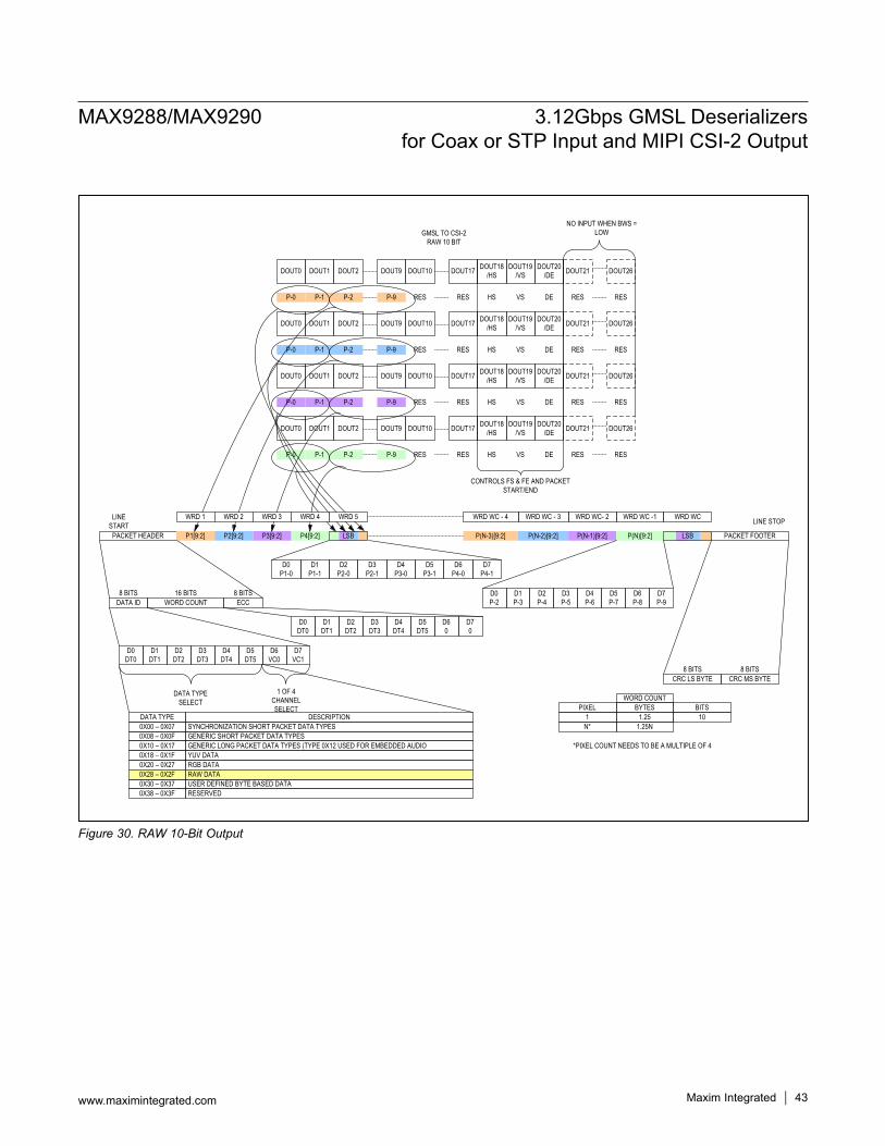
MAX9288/MAX9290 3.12Gbps GMSL Deserializers for Coax or STP Input and MIPI CSI-2 Output
www.maximintegrated.com Maxim Integrated 43
Figure 30. RAW 10-Bit Output
DOUT0 DOUT1
P-0 P-1 P-2
DOUT2 DOUT10
GMSL TO CSI-2RAW 10 BIT
HS VS DE
DOUT18/HS
DOUT19/VS
DOUT20/DE DOUT21 DOUT26
RES RES
DOUT17
RES
NO INPUT WHEN BWS = LOW
DOUT0 DOUT1
P-0 P-1 P-2
DOUT2 DOUT10
HS VS DE
DOUT18/HS
DOUT19/VS
DOUT20/DE DOUT21 DOUT26
RES RES
DOUT17
RES
CONTROLS FS & FE AND PACKET START/END
DOUT0 DOUT1 DOUT2 DOUT10
HS VS DE
DOUT18/HS
DOUT19/VS
DOUT20/DE DOUT21 DOUT26
RES RES
DOUT17
RES
DOUT0 DOUT1 DOUT2 DOUT10
P-0 P-1 P-2
HS VS DE
DOUT18/HS
DOUT19/VS
DOUT20/DE DOUT21 DOUT26
RES RES
DOUT17
RES
P-0 P-1 P-2
RES
RES
RES
RES
DOUT9
P-9
DOUT9
P-9
DOUT9
DOUT9
P-9
P-9
P4[9:2]PACKET HEADER P1[9:2] P3[9:2]P2[9:2] P(N-3)[9:2] P(N-2)[9:2] P(N)[9:2]P(N-1)[9:2] PACKET FOOTER
DATA ID WORD COUNT ECC
D5 P3-1
D4 P3-0
D3 P2-1
D2 P2-0
D1 P1-1
D0 P1-0
D7 P4-1
D6 P4-0
8 BITS 16 BITS 8 BITS
D70
D60
D5DT5
D4DT4
D3DT3
D2DT2
D1DT1
D0DT0
D7VC1
D6VC0
D5DT5
D4DT4
D3DT3
D2DT2
D1DT1
D0DT0
CRC LS BYTE CRC MS BYTE
DATA TYPE0X00 – 0X070X08 – 0X0F0X10 – 0X170X18 – 0X1F
0X30 – 0X370X38 – 0X3F
0X20 – 0X270X28 – 0X2F
DESCRIPTIONSYNCHRONIZATION SHORT PACKET DATA TYPESGENERIC SHORT PACKET DATA TYPESGENERIC LONG PACKET DATA TYPES (TYPE 0X12 USED FOR EMBEDDED AUDIOYUV DATA
USER DEFINED BYTE BASED DATARESERVED
RGB DATARAW DATA
1 OF 4 CHANNEL SELECT
DATA TYPE SELECT
8 BITS 8 BITS
WORD COUNTPIXEL BYTES BITS
1 1.25 10
LINE START LINE STOP
N* 1.25N
WRD 1 WRD 2 WRD 3 WRD 4 WRD WC- 2 WRD WC -1 WRD WCWRD WC - 3WRD 5
LSB LSB
WRD WC - 4
D6 P-8
D7 P-9
D0 P-2
D1 P-3
D2 P-4
D3 P-5
D4 P-6
D5 P-7
*PIXEL COUNT NEEDS TO BE A MULTIPLE OF 4
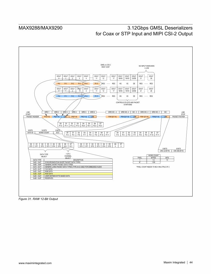
MAX9288/MAX9290 3.12Gbps GMSL Deserializers for Coax or STP Input and MIPI CSI-2 Output
www.maximintegrated.com Maxim Integrated 44
Figure 31. RAW 12-Bit Output
DOUT0
DOUT1
P-0 P-1 P-2
DOUT2
GMSL to CSI-2RAW 12 BIT
P4[11:4]PACKET HEADER P1[11:4] P3[11:4]P2[11:4] P(N-3)[11:4] P(N-2)[11:4] P(N)[11:4]P(N-1)[11:4] PACKET FOOTER
DATA ID WORD COUNT ECC8 BITS 16 BITS 8 BITS
D70
D60
D5DT5
D4DT4
D3DT3
D2DT2
D1DT1
D0DT0
D7VC1
D6VC0
D5DT5
D4DT4
D3DT3
D2DT2
D1DT1
D0DT0
CRC LS BYTE CRC MS BYTE
DATA TYPE0x00 – 0x070x08 – 0x0F0x10 – 0x170x18 – 0x1F
0x30 – 0x370x38 – 0x3F
0x20 – 0x270x28 – 0x2F
DESCRIPTIONSYNCHRONIZATION SHORT PACKET DATA TYPESGENERIC SHORT PACKET DATA TYPESGENERIC LONG PACKET DATA TYPES (TYPE 0x12 USED FOR EMBEDDED AUDIOYUV DATA
USER DEFINED BYTE BASED DATARESERVED
RGB DATARAW DATA
1 OF 4 CHANNEL SELECT
DATA TYPE SELECT
8 BITS 8 BITS
WORD COUNTPIXEL BYTES BITS
1 1.5 12
LINE START
LINE STOP
N* 1.5N
WRD WC- 2 WRD WC -1 WCWC - 3
D3 P-7
D2 P-6
D1 P-5
D0 P-4
D7 P-11
D6 P-10
D5 P-9
D4 P-8
HS VS DE
DOUT18/HS
DOUT19/VS
DOUT20/DE
CONTROLS FS & FE AND PACKET START/END
DOUT11
P-11
WRD 5
LSB
WRD WC- 4
*PIXEL COUNT NEEDS TO BE A MULTIPLE OF 2
DOUT3
P-3 P-4
DOUT4
DOUT0
DOUT1
P-0 P-1 P-2
DOUT2
HS VS DE
DOUT18/HS
DOUT19/VS
DOUT20/DE
DOUT11
P-11
DOUT3
P-3 P-4
DOUT4
LSB LSB LSB
WRD 6 WRD WC - 4
DOUT21
DOUT26
RES RES
NO INPUT WHEN BWS = LOW
DOUT12
DOUT17
RES RES
DOUT12
DOUT17
RES RES
DOUT21
DOUT26
RES RES
D3 P-7
D2 P-6
D1 P-5
D0 P-4
D7 P-11
D6 P-10
D5 P-9
D4 P-8
D7 P2-3
D6 P2-2
D3 P1-3
D2 P1-2
D5 P2-1
D4 P2-0
D1 P1-1
D0 P1-0
WRD 1 WRD 2 WRD 3 WRD 4
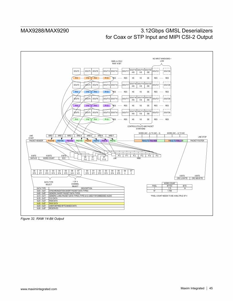
MAX9288/MAX9290 3.12Gbps GMSL Deserializers for Coax or STP Input and MIPI CSI-2 Output
www.maximintegrated.com Maxim Integrated 45
Figure 32. RAW 14-Bit Output
DOUT0
P-0
DOUT14
GMSL to CSI-2RAW 14 BIT
HS VS DE
DOUT18/HS
DOUT19/VS
DOUT20/DE DOUT21 DOUT26
RES RES
DOUT17
RES
NO INPUT WHEN BWS = LOW
DOUT0
P-0
DOUT14
HS VS DE
DOUT18/HS
DOUT19/VS
DOUT20/DE DOUT21 DOUT26
RES RES
DOUT17
RES
CONTROLS FS & FE AND PACKET START/END
DOUT0 DOUT14
HS VS DE
DOUT18/HS
DOUT19/VS
DOUT20/DE DOUT21 DOUT26
RES RES
DOUT17
RES
DOUT0 DOUT14
P-0
HS VS DE
DOUT18/HS
DOUT19/VS
DOUT20/DE DOUT21 DOUT26
RES RES
DOUT17
RES
P-0 RES
DOUT5
P-5
DOUT5
P-5
DOUT5
DOUT5
P-5
P-5
P4[13:6]PACKET HEADER P1[13:6] P3[13:6]P2[13:6] PACKET FOOTER
DATA ID WORD COUNT ECCP-2 P-3 P-4 P-5P-0 P-18 BITS 16 BITS 8 BITS
D70
D60
D5DT5
D4DT4
D3DT3
D2DT2
D1DT1
D0DT0
D7VC1
D6VC0
D5DT5
D4DT4
D3DT3
D2DT2
D1DT1
D0DT0
CRC LS BYTE CRC MS BYTE
DATA TYPE0x00 – 0x070x08 – 0x0F0x10 – 0x170x18 – 0x1F
0x30 – 0x370x38 – 0x3F
0x20 – 0x270x28 – 0x2F
DESCRIPTIONSYNCHRONIZATION SHORT PACKET DATA TYPESGENERIC SHORT PACKET DATA TYPESGENERIC LONG PACKET DATA TYPES (TYPE 0x12 USED FOR EMBEDDED AUDIOYUV DATA
USER DEFINED BYTE BASED DATARESERVED
RGB DATARAW DATA
1 OF 4 CHANNEL SELECT
DATA TYPE SELECT
8 BITS 8 BITS
WORD COUNTPIXEL BYTES BITS
1 1.75 14
LINE START LINE STOP
N* 1.75N
WRD 1 WRD 2 WRD 3 WRD 4 WRD 5WORD (WC – 6) TO (WC – 3)
D7 P-13
D0 P-6
D1 P-7
*PIXEL COUNT NEEDS TO BE A MULTIPLE OF 4
MSBLSB
P4[5:0]P1[5:0] P3[5:0]P2[5:0] P(N-3) TO P(N) LSBP(N-3) TO P(N) MSB
WORD (WC – 2) TO WCWRD 6 WRD 7
DOUT6
P-6
DOUT6
P-6
DOUT6
DOUT6
P-6
P-6
DOUT13
P-13
DOUT13
P-13
DOUT13
DOUT13
P-13
P-13
RES
RES
RES
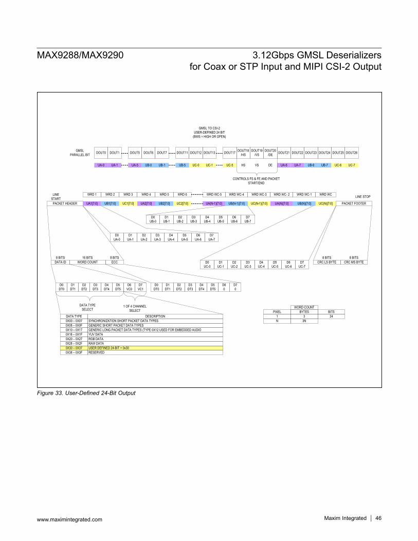
MAX9288/MAX9290 3.12Gbps GMSL Deserializers for Coax or STP Input and MIPI CSI-2 Output
www.maximintegrated.com Maxim Integrated 46
Figure 33. User-Defined 24-Bit Output
HS VS DE
CONTROLS FS & FE AND PACKET START/END
DOUT0 DOUT1 DOUT18/HS
DOUT19/VS
DOUT20/DE DOUT21 DOUT22 DOUT23 DOUT24 DOUT25 DOUT26GMSL
PARALLEL BIT
UA-0 UA-1 UA-5
DOUT5 DOUT6 DOUT7 DOUT11 DOUT12 DOUT13 DOUT17
UB-0 UB-1 UB-5 UC-0 UC-1 UC-5 UA-6 UA-7 UB-6 UB-7 UC-6 UC-7
GMSL TO CSI-2USER-DEFINED 24 BIT
(BWS = HIGH OR OPEN)
UA2[7:0]PACKET HEADER UC2[7:0]UB2[7:0]UA1[7:0] UC1[7:0]UB1[7:0] UA(N-1)[7:0] UC(N-1)[7:0]UB(N-1)[7:0] UA(N)[7:0] UC(N)[7:0]UB(N)[7:0] PACKET FOOTER
DATA ID WORD COUNT ECC8 BITS 16 BITS 8 BITS
D70
D60
D5DT5
D4DT4
D3DT3
D2DT2
D1DT1
D0DT0
D7VC1
D6VC0
D5DT5
D4DT4
D3DT3
D2DT2
D1DT1
D0DT0
CRC LS BYTE CRC MS BYTE
DATA TYPE0X00 – 0X070X08 – 0X0F0X10 – 0X170X18 – 0X1F
0X30 – 0X370X38 – 0X3F
0X20 – 0X270X28 – 0X2F
DESCRIPTIONSYNCHRONIZATION SHORT PACKET DATA TYPESGENERIC SHORT PACKET DATA TYPESGENERIC LONG PACKET DATA TYPES (TYPE 0X12 USED FOR EMBEDDED AUDIOYUV DATA
USER DEFINED 24-BIT = 0x30RESERVED
RGB DATARAW DATA
1 OF 4 CHANNEL SELECT
DATA TYPE SELECT
8 BITS 8 BITS
WORD COUNTPIXEL BYTES BITS
1 3 24
LINE START LINE STOP
N 3N
WRD 1 WRD 2 WRD 3 WRD 4 WRD WC- 2 WRD WC-1 WRD WCWRD WC-4WRD 5 WRD 6 WRD WC-5 WRD WC-3
D0 UB-0
D1 UB-1
D2 UB-2
D3 UB-3
D4 UB-4
D5 UB-5
D6 UB-6
D7 UB-7
D0 UA-0
D1 UA-1
D2 UA-2
D3 UA-3
D4 UA-4
D5 UA-5
D6 UA-6
D7 UA-7
D0 UC-0
D1 UC-1
D2 UC-2
D3 UC-3
D4 UC-4
D5 UC-5
D6 UC-6
D7 UC-7
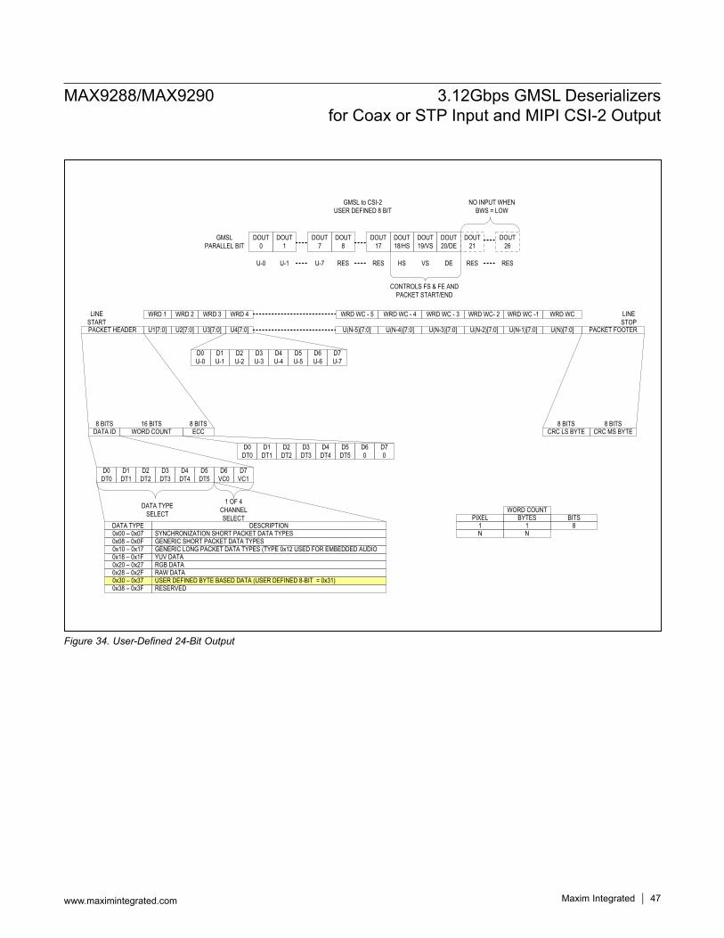
MAX9288/MAX9290 3.12Gbps GMSL Deserializers for Coax or STP Input and MIPI CSI-2 Output
www.maximintegrated.com Maxim Integrated 47
Figure 34. User-Defined 24-Bit Output
DOUT0
DOUT1
GMSLPARALLEL BIT
U-0 U-1 U-7
DOUT7
DOUT8
GMSL to CSI-2USER DEFINED 8 BIT
U4[7:0]PACKET HEADER U1[7:0] U3[7:0]U2[7:0] U(N-5)[7:0] U(N-3)[7:0]U(N-4)[7:0] U(N-2)[7:0] U(N)[7:0]U(N-1)[7:0] PACKET FOOTER
DATA ID WORD COUNT ECC8 BITS 16 BITS 8 BITS
D70
D60
D5DT5
D4DT4
D3DT3
D2DT2
D1DT1
D0DT0
D7VC1
D6VC0
D5DT5
D4DT4
D3DT3
D2DT2
D1DT1
D0DT0
CRC LS BYTE CRC MS BYTE
DATA TYPE0x00 – 0x070x08 – 0x0F0x10 – 0x170x18 – 0x1F
0x30 – 0x370x38 – 0x3F
0x20 – 0x270x28 – 0x2F
DESCRIPTIONSYNCHRONIZATION SHORT PACKET DATA TYPESGENERIC SHORT PACKET DATA TYPESGENERIC LONG PACKET DATA TYPES (TYPE 0x12 USED FOR EMBEDDED AUDIOYUV DATA
USER DEFINED BYTE BASED DATA (USER DEFINED 8-BIT = 0x31)RESERVED
RGB DATARAW DATA
1 OF 4 CHANNEL SELECT
DATA TYPE SELECT
8 BITS 8 BITS
WORD COUNTPIXEL BYTES BITS
1 1 8
LINE START
LINE STOP
N N
WRD 1 WRD 2 WRD 3 WRD 4 WRD WC- 2 WRD WC -1 WRD WCWRD WC - 4WRD WC - 5 WRD WC - 3
D7U-7
D6U-6
D5U-5
D4U-4
D3U-3
D2U-2
D1U-1
D0U-0
HS VS DE
CONTROLS FS & FE AND PACKET START/END
DOUT18/HS
DOUT19/VS
DOUT20/DE
DOUT17
DOUT21
DOUT26
RES RES
NO INPUT WHEN BWS = LOW
RESRES
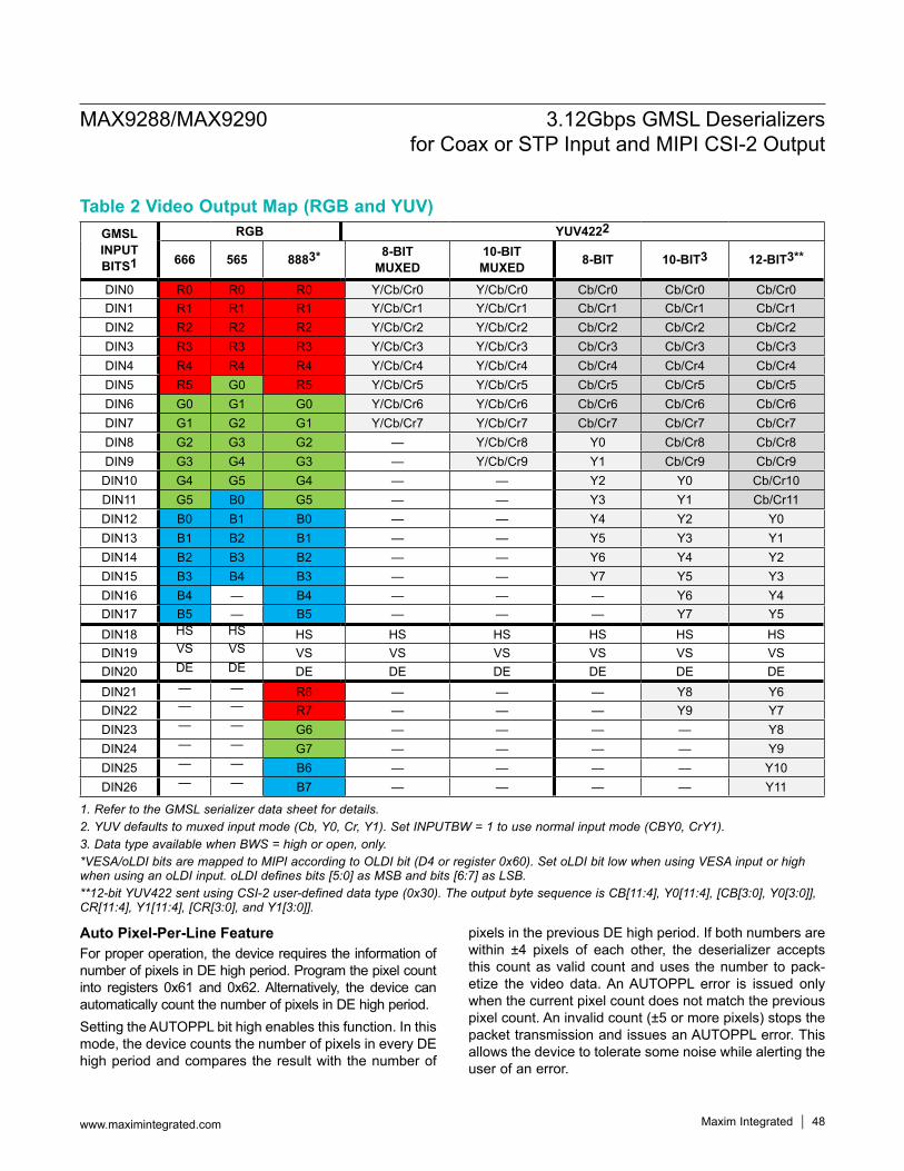
MAX9288/MAX9290 3.12Gbps GMSL Deserializers for Coax or STP Input and MIPI CSI-2 Output
www.maximintegrated.com Maxim Integrated 48
Auto Pixel-Per-Line FeatureFor proper operation, the device requires the information of number of pixels in DE high period. Program the pixel count into registers 0x61 and 0x62. Alternatively, the device can automatically count the number of pixels in DE high period.Setting the AUTOPPL bit high enables this function. In this mode, the device counts the number of pixels in every DE high period and compares the result with the number of
pixels in the previous DE high period. If both numbers are within ±4 pixels of each other, the deserializer accepts this count as valid count and uses the number to pack-etize the video data. An AUTOPPL error is issued only when the current pixel count does not match the previous pixel count. An invalid count (±5 or more pixels) stops the packet transmission and issues an AUTOPPL error. This allows the device to tolerate some noise while alerting the user of an error.
Table 2 Video Output Map (RGB and YUV)
1. Refer to the GMSL serializer data sheet for details.2. YUV defaults to muxed input mode (Cb, Y0, Cr, Y1). Set INPUTBW = 1 to use normal input mode (CBY0, CrY1).3. Data type available when BWS = high or open, only.*VESA/oLDI bits are mapped to MIPI according to OLDI bit (D4 or register 0x60). Set oLDI bit low when using VESA input or high when using an oLDI input. oLDI defines bits [5:0] as MSB and bits [6:7] as LSB.**12-bit YUV422 sent using CSI-2 user-defined data type (0x30). The output byte sequence is CB[11:4], Y0[11:4], [CB[3:0], Y0[3:0]], CR[11:4], Y1[11:4], [CR[3:0], and Y1[3:0]].
GMSL INPUT BITS1
RGB YUV4222
666 565 8883* 8-BITMUXED
10-BITMUXED 8-BIT 10-BIT3 12-BIT3**
DIN0 R0 R0 R0 Y/Cb/Cr0 Y/Cb/Cr0 Cb/Cr0 Cb/Cr0 Cb/Cr0DIN1 R1 R1 R1 Y/Cb/Cr1 Y/Cb/Cr1 Cb/Cr1 Cb/Cr1 Cb/Cr1DIN2 R2 R2 R2 Y/Cb/Cr2 Y/Cb/Cr2 Cb/Cr2 Cb/Cr2 Cb/Cr2DIN3 R3 R3 R3 Y/Cb/Cr3 Y/Cb/Cr3 Cb/Cr3 Cb/Cr3 Cb/Cr3DIN4 R4 R4 R4 Y/Cb/Cr4 Y/Cb/Cr4 Cb/Cr4 Cb/Cr4 Cb/Cr4DIN5 R5 G0 R5 Y/Cb/Cr5 Y/Cb/Cr5 Cb/Cr5 Cb/Cr5 Cb/Cr5DIN6 G0 G1 G0 Y/Cb/Cr6 Y/Cb/Cr6 Cb/Cr6 Cb/Cr6 Cb/Cr6DIN7 G1 G2 G1 Y/Cb/Cr7 Y/Cb/Cr7 Cb/Cr7 Cb/Cr7 Cb/Cr7DIN8 G2 G3 G2 — Y/Cb/Cr8 Y0 Cb/Cr8 Cb/Cr8DIN9 G3 G4 G3 — Y/Cb/Cr9 Y1 Cb/Cr9 Cb/Cr9
DIN10 G4 G5 G4 — — Y2 Y0 Cb/Cr10DIN11 G5 B0 G5 — — Y3 Y1 Cb/Cr11DIN12 B0 B1 B0 — — Y4 Y2 Y0DIN13 B1 B2 B1 — — Y5 Y3 Y1DIN14 B2 B3 B2 — — Y6 Y4 Y2DIN15 B3 B4 B3 — — Y7 Y5 Y3DIN16 B4 — B4 — — — Y6 Y4DIN17 B5 — B5 — — — Y7 Y5DIN18 HS HS HS HS HS HS HS HSDIN19 VS VS VS VS VS VS VS VSDIN20 DE DE DE DE DE DE DE DEDIN21 — — R6 — — — Y8 Y6DIN22 — — R7 — — — Y9 Y7DIN23 — — G6 — — — — Y8DIN24 — — G7 — — — — Y9DIN25 — — B6 — — — — Y10DIN26 — — B7 — — — — Y11
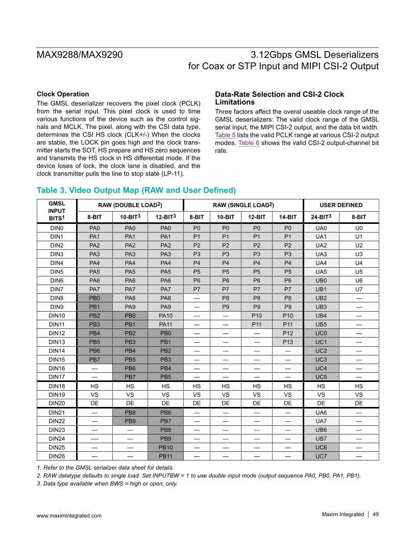
MAX9288/MAX9290 3.12Gbps GMSL Deserializers for Coax or STP Input and MIPI CSI-2 Output
www.maximintegrated.com Maxim Integrated 49
Clock OperationThe GMSL deserializer recovers the pixel clock (PCLK) from the serial input. This pixel clock is used to time various functions of the device such as the control sig-nals and MCLK. The pixel, along with the CSI data type, determines the CSI HS clock (CLK+/-) When the clocks are stable, the LOCK pin goes high and the clock trans-mitter starts the SOT, HS prepare and HS zero sequences and transmits the HS clock in HS differential mode. If the device loses of lock, the clock lane is disabled, and the clock transmitter pulls the line to stop state (LP-11).
Data-Rate Selection and CSI-2 Clock LimitationsThree factors affect the overal useable clock range of the GMSL deserializers: The valid clock range of the GMSL serial input, the MIPI CSI-2 output, and the data bit width. Table 5 lists the valid PCLK range at various CSI-2 output modes. Table 6 shows the valid CSI-2 output-channel bit rate.
Table 3. Video Output Map (RAW and User Defined)
1. Refer to the GMSL serializer data sheet for details.2. RAW datatype defaults to single load. Set INPUTBW = 1 to use double input mode (output sequence PA0, PB0, PA1, PB1).3. Data type available when BWS = high or open, only.
GMSL INPUT BITS1
RAW (DOUBLE LOAD2) RAW (SINGLE LOAD2) USER DEFINED
8-BIT 10-BIT3 12-BIT3 8-BIT 10-BIT 12-BIT 14-BIT 24-BIT3 8-BIT
DIN0 PA0 PA0 PA0 P0 P0 P0 P0 UA0 U0DIN1 PA1 PA1 PA1 P1 P1 P1 P1 UA1 U1DIN2 PA2 PA2 PA2 P2 P2 P2 P2 UA2 U2DIN3 PA3 PA3 PA3 P3 P3 P3 P3 UA3 U3DIN4 PA4 PA4 PA4 P4 P4 P4 P4 UA4 U4DIN5 PA5 PA5 PA5 P5 P5 P5 P5 UA5 U5DIN6 PA6 PA6 PA6 P6 P6 P6 P6 UB0 U6DIN7 PA7 PA7 PA7 P7 P7 P7 P7 UB1 U7DIN8 PB0 PA8 PA8 — P8 P8 P8 UB2 —DIN9 PB1 PA9 PA9 — P9 P9 P9 UB3 —
DIN10 PB2 PB0 PA10 — — P10 P10 UB4 —DIN11 PB3 PB1 PA11 — — P11 P11 UB5 —DIN12 PB4 PB2 PB0 — — — P12 UC0 —DIN13 PB5 PB3 PB1 — — — P13 UC1 —DIN14 PB6 PB4 PB2 — — — — UC2 —DIN15 PB7 PB5 PB3 — — — — UC3 —DIN16 — PB6 PB4 — — — — UC4 —DIN17 — PB7 PB5 — — — — UC5 —DIN18 HS HS HS HS HS HS HS HS HSDIN19 VS VS VS VS VS VS VS VS VSDIN20 DE DE DE DE DE DE DE DE DEDIN21 — PB8 PB6 — — — — UA6 —DIN22 — PB9 PB7 — — — — UA7 —DIN23 — — PB8 — — — — UB6 —DIN24 —- — PB9 — — — — UB7 —DIN25 — — PB10 — — — — UC6 —DIN26 — — PB11 — — — — UC7 —
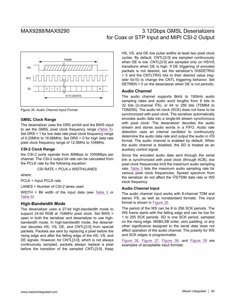
MAX9288/MAX9290 3.12Gbps GMSL Deserializers for Coax or STP Input and MIPI CSI-2 Output
www.maximintegrated.com Maxim Integrated 50
GMSL Clock RangeThe deserializer uses the DRS pin/bit and the BWS input to set the GMSL pixel clock frequency range (Table 5). Set DRS = 1 for low data rate pixel clock frequency range of 6.25MHz to 16.66MHz. Set DRS = 0 for high data rate pixel clock frequency range of 12.5MHz to 104MHz.
CSI-2 Clock Rangethe CSI-2 ports operate from 80Mbps to 1000Mbps per channel. The CSI-2 output bit rate can be calculated from the PCLK rate by the following equation:
CSI RATE = PCLK x WIDTH/LANESwhere:PCLK = Input PCLK rateLANES = Number of CSI-2 lanes usedWIDTH = Bit width of the input data (see Table 5 or Table 6)
High-Bandwidth ModeThe deserializer uses a 27-bit high-bandwidth mode to support 24-bit RGB at 104MHz pixel clock. Set BWS = open in both the serializer and deserializer to use high-bandwidth mode. In high-bandwidth mode, the deserial-izer decodes HS, VS, DE, and CNTL[3:0] from special packets. Packets are sent by replacing a pixel before the rising edge and after the falling edge of the HS, VS, and DE signals. However, for CNTL[3:0], which is not always continuously sampled, packets always replace a pixel before the transition of the sampled CNTL[3:0]. Keep
HS, VS, and DE low pulse widths at least two pixel clock cycles. By default, CNTL[3:0] are sampled continuously when DE is low. CNTL[3:0] are sampled only on HS/VS transitions when DE is high. If DE triggering of encoded packets is not desired, set the serializer’s DISDETRIG = 0 and the CNTLTRIG bits to their desired value (reg-ister 0x15) to change the CNTL triggering behavior. Set DETREN = 0 on the deserializer when DE is not periodic.
Audio ChannelThe audio channel supports 8kHz to 192kHz audio sampling rates and audio word lengths from 8 bits to 32 bits (2-channel I2S), or 64 to 256 bits (TDM64 to TDM256). The audio bit clock (SCK) does not have to be synchronized with pixel clock. The serializer automatically encodes audio data into a single-bit stream synchronous with pixel clock. The deserializer decodes the audio stream and stores audio words in a FIFO. Audio rate detection uses an internal oscillator to continuously determine the audio data rate and output the audio in I2S format. The audio channel is enabled by default. When the audio channel is disabled, the SD is treated as an auxiliary control signal.Since the encoded audio data sent through the serial link is synchronized with pixel clock (through ACB), low pixel clock frequencies limit the maximum audio sampling rate. Table 5 lists the maximum audio sampling rate for various pixel clock frequencies. Spread spectrum from the serializer do not affect the I2S/TDM data rate or WS clock frequency.
Audio Channel InputThe audio channel input works with 8-channel TDM and stereo I2S, as well as nonstandard formats. The input format is shown in Figure 35.The period of the WS can be 8 to 256 SCK periods. The WS frame starts with the falling edge and can be low for 1 to 255 SCK periods. SD is one SCK period, sampled on the rising edge. MSB/LSB order, zero padding, or any other significance assigned to the serial data does not affect operation of the audio channel. The polarity for WS and SCK edges is programmable.Figure 36, Figure 37, Figure 38, and Figure 39 are examples of acceptable input formats.
Figure 35. Audio Channel Input Format
FRAME
16 TO 256 BITS
0 1 2
SCK
SD
WS
N
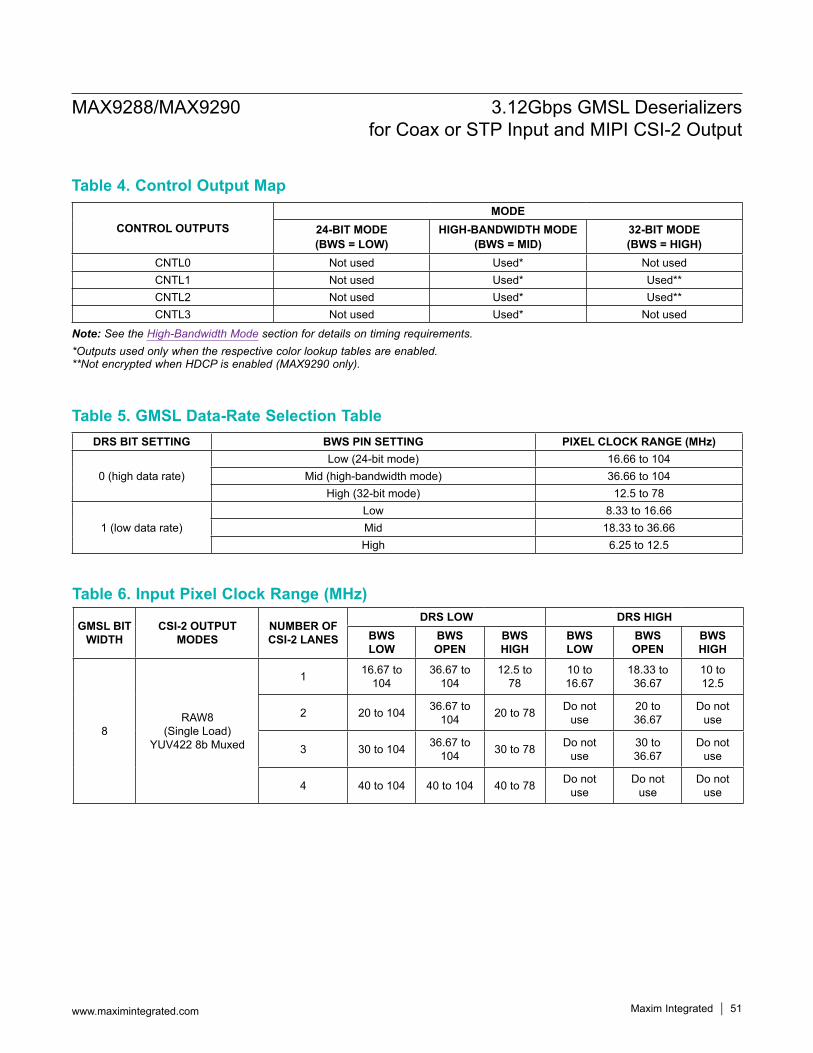
MAX9288/MAX9290 3.12Gbps GMSL Deserializers for Coax or STP Input and MIPI CSI-2 Output
www.maximintegrated.com Maxim Integrated 51
Table 5. GMSL Data-Rate Selection Table
Table 4. Control Output Map
Note: See the High-Bandwidth Mode section for details on timing requirements.*Outputs used only when the respective color lookup tables are enabled. **Not encrypted when HDCP is enabled (MAX9290 only).
Table 6. Input Pixel Clock Range (MHz)
CONTROL OUTPUTSMODE
24-BIT MODE (BWS = LOW)
HIGH-BANDWIDTH MODE (BWS = MID)
32-BIT MODE (BWS = HIGH)
CNTL0 Not used Used* Not usedCNTL1 Not used Used* Used**CNTL2 Not used Used* Used**CNTL3 Not used Used* Not used
DRS BIT SETTING BWS PIN SETTING PIXEL CLOCK RANGE (MHz)
0 (high data rate)Low (24-bit mode) 16.66 to 104
Mid (high-bandwidth mode) 36.66 to 104High (32-bit mode) 12.5 to 78
1 (low data rate)Low 8.33 to 16.66Mid 18.33 to 36.66High 6.25 to 12.5
GMSL BIT WIDTH
CSI-2 OUTPUT MODES
NUMBER OF CSI-2 LANES
DRS LOW DRS HIGHBWS LOW
BWS OPEN
BWS HIGH
BWS LOW
BWS OPEN
BWS HIGH
8RAW8
(Single Load) YUV422 8b Muxed
1 16.67 to 104
36.67 to 104
12.5 to 78
10 to 16.67
18.33 to 36.67
10 to 12.5
2 20 to 104 36.67 to 104 20 to 78 Do not
use20 to 36.67
Do not use
3 30 to 104 36.67 to 104 30 to 78 Do not
use30 to 36.67
Do not use
4 40 to 104 40 to 104 40 to 78 Do not use
Do not use
Do not use
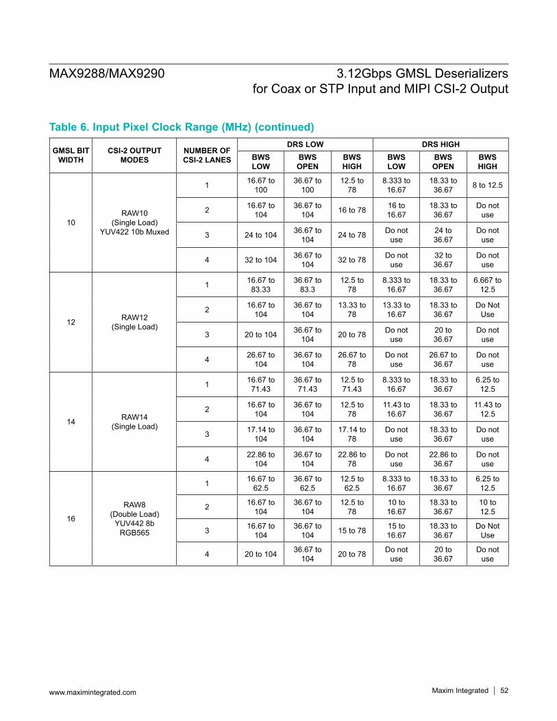
MAX9288/MAX9290 3.12Gbps GMSL Deserializers for Coax or STP Input and MIPI CSI-2 Output
www.maximintegrated.com Maxim Integrated 52
Table 6. Input Pixel Clock Range (MHz) (continued)
GMSL BIT WIDTH
CSI-2 OUTPUT MODES
NUMBER OF CSI-2 LANES
DRS LOW DRS HIGHBWS LOW
BWS OPEN
BWS HIGH
BWS LOW
BWS OPEN
BWS HIGH
10RAW10
(Single Load) YUV422 10b Muxed
1 16.67 to 100
36.67 to 100
12.5 to 78
8.333 to 16.67
18.33 to 36.67 8 to 12.5
2 16.67 to 104
36.67 to 104 16 to 78 16 to
16.6718.33 to 36.67
Do not use
3 24 to 104 36.67 to 104 24 to 78 Do not
use24 to 36.67
Do not use
4 32 to 104 36.67 to 104 32 to 78 Do not
use32 to 36.67
Do not use
12 RAW12 (Single Load)
1 16.67 to 83.33
36.67 to 83.3
12.5 to 78
8.333 to 16.67
18.33 to 36.67
6.667 to 12.5
2 16.67 to 104
36.67 to 104
13.33 to 78
13.33 to 16.67
18.33 to 36.67
Do Not Use
3 20 to 104 36.67 to 104 20 to 78 Do not
use20 to 36.67
Do not use
4 26.67 to 104
36.67 to 104
26.67 to 78
Do not use
26.67 to 36.67
Do not use
14 RAW14 (Single Load)
1 16.67 to 71.43
36.67 to 71.43
12.5 to 71.43
8.333 to 16.67
18.33 to 36.67
6.25 to 12.5
2 16.67 to 104
36.67 to 104
12.5 to 78
11.43 to 16.67
18.33 to 36.67
11.43 to 12.5
3 17.14 to 104
36.67 to 104
17.14 to 78
Do not use
18.33 to 36.67
Do not use
4 22.86 to 104
36.67 to 104
22.86 to 78
Do not use
22.86 to 36.67
Do not use
16
RAW8 (Double Load)
YUV442 8b RGB565
1 16.67 to 62.5
36.67 to 62.5
12.5 to 62.5
8.333 to 16.67
18.33 to 36.67
6.25 to 12.5
2 16.67 to 104
36.67 to 104
12.5 to 78
10 to 16.67
18.33 to 36.67
10 to 12.5
3 16.67 to 104
36.67 to 104 15 to 78 15 to
16.6718.33 to 36.67
Do Not Use
4 20 to 104 36.67 to 104 20 to 78 Do not
use20 to 36.67
Do not use
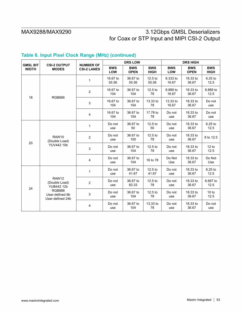
MAX9288/MAX9290 3.12Gbps GMSL Deserializers for Coax or STP Input and MIPI CSI-2 Output
www.maximintegrated.com Maxim Integrated 53
Table 6. Input Pixel Clock Range (MHz) (continued)
GMSL BIT WIDTH
CSI-2 OUTPUT MODES
NUMBER OF CSI-2 LANES
DRS LOW DRS HIGHBWS LOW
BWS OPEN
BWS HIGH
BWS LOW
BWS OPEN
BWS HIGH
18 RGB666
1 16.67 to 55.56
36.67 to 55.56
12.5 to 55.56
8.333 to 16.67
18.33 to 36.67
6.25 to 12.5
2 16.67 to 104
36.67 to 104
12.5 to 78
8.889 to 16.67
18.33 to 36.67
8.889 to 12.5
3 16.67 to 104
36.67 to 104
13.33 to 78
13.33 to 16.67
18.33 to 36.67
Do not use
4 16.67 to 104
36.67 to 104
17.78 to 78
Do not use
18.33 to 36.67
Do not use
20
RAW10 (Double Load) YUV442 10b
1 Do not use
36.67 to 50
12.5 to 50
Do not use
18.33 to 36.67
6.25 to 12.5
2 Do not use
36.67 to 100
12.5 to 78
Do not use
18.33 to 36.67 8 to 12.5
3 Do not use
36.67 to 104
12.5 to 78
Do not use
18.33 to 36.67
12 to 12.5
4 Do not use
36.67 to 104 16 to 78 Do Not
Use18.33 to 36.67
Do Not Use
24
RAW12 (Double Load) YUB442 12b
RGB888 User-defined 8b
User-defined 24b
1 Do not use
36.67 to 41.67
12.5 to 41.67
Do not use
18.33 to 36.67
6.25 to 12.5
2 Do not use
36.67 to 83.33
12.5 to 78
Do not use
18.33 to 36.67
6.667 to 12.5
3 Do not use
36.67 to 104
12.5 to 78
Do not use
18.33 to 36.67
10 to 12.5
4 Do not use
36.67 to 104
13,33 to 78
Do not use
18.33 to 36.67
Do not use
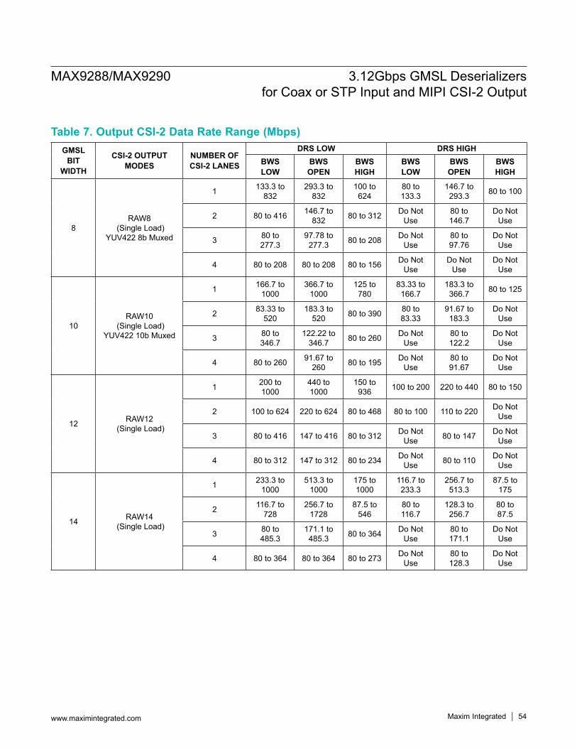
MAX9288/MAX9290 3.12Gbps GMSL Deserializers for Coax or STP Input and MIPI CSI-2 Output
www.maximintegrated.com Maxim Integrated 54
Table 7. Output CSI-2 Data Rate Range (Mbps)GMSL
BIT WIDTH
CSI-2 OUTPUT MODES
NUMBER OF CSI-2 LANES
DRS LOW DRS HIGHBWS LOW
BWS OPEN
BWS HIGH
BWS LOW
BWS OPEN
BWS HIGH
8RAW8
(Single Load) YUV422 8b Muxed
1 133.3 to 832
293.3 to 832
100 to 624
80 to 133.3
146.7 to 293.3 80 to 100
2 80 to 416 146.7 to 832 80 to 312 Do Not
Use80 to 146.7
Do Not Use
3 80 to 277.3
97.78 to 277.3 80 to 208 Do Not
Use80 to 97.76
Do Not Use
4 80 to 208 80 to 208 80 to 156 Do Not Use
Do Not Use
Do Not Use
10RAW10
(Single Load) YUV422 10b Muxed
1 166.7 to 1000
366.7 to 1000
125 to 780
83.33 to 166.7
183.3 to 366.7 80 to 125
2 83.33 to 520
183.3 to 520 80 to 390 80 to
83.3391.67 to 183.3
Do Not Use
3 80 to 346.7
122.22 to 346.7 80 to 260 Do Not
Use80 to 122.2
Do Not Use
4 80 to 260 91.67 to 260 80 to 195 Do Not
Use80 to 91.67
Do Not Use
12 RAW12 (Single Load)
1 200 to 1000
440 to 1000
150 to 936 100 to 200 220 to 440 80 to 150
2 100 to 624 220 to 624 80 to 468 80 to 100 110 to 220 Do Not Use
3 80 to 416 147 to 416 80 to 312 Do Not Use 80 to 147 Do Not
Use
4 80 to 312 147 to 312 80 to 234 Do Not Use 80 to 110 Do Not
Use
14 RAW14 (Single Load)
1 233.3 to 1000
513.3 to 1000
175 to 1000
116.7 to 233.3
256.7 to 513.3
87.5 to 175
2 116.7 to 728
256.7 to 1728
87.5 to 546
80 to 116.7
128.3 to 256.7
80 to 87.5
3 80 to 485.3
171.1 to 485.3 80 to 364 Do Not
Use80 to 171.1
Do Not Use
4 80 to 364 80 to 364 80 to 273 Do Not Use
80 to 128.3
Do Not Use
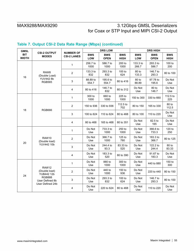
MAX9288/MAX9290 3.12Gbps GMSL Deserializers for Coax or STP Input and MIPI CSI-2 Output
www.maximintegrated.com Maxim Integrated 55
Table 7. Output CSI-2 Data Rate Range (Mbps) (continued) GMSL
BIT WIDTH
CSI-2 OUTPUT MODES
NUMBER OF CSI-2 LANES
DRS LOW DRS HIGHBWS LOW
BWS OPEN
BWS HIGH
BWS LOW
BWS OPEN
BWS HIGH
16
RAW8 (Double Load)
YUV442 8b RGB565
1 256.7 to 1000
586.7 to 1000
200 to 1000
133.3 to 266.7
293.3 to 586.7
100 to 200
2 133.3 to 832
293.3 to 832
100 to 624
80 to 133.3
146.7 to 293.3 80 to 100
3 88.89 to 554.7
195.6 to 554.7 80 to 416 80 to
88.8997.78 to 195.6
Do Not Use
4 80 to 416 146.7 to 832 80 to 312 Do Not
Use80 to 146.7
Do Not Use
18 RGB666
1 300 to 1000
660 to 1000
225 to 1000 150 to 300 330 to 660 112.5 to
225
2 150 to 936 330 to 936 112.5 to 702 80 to 150 165 to 330 80 to
112.5
3 100 to 624 110 to 624 80 to 468 80 to 100 110 to 220 Do Not Use
4 80 to 468 165 to 468 80 to 351 Do Not Use
82.5 to 165
Do Not Use
20
RAW10 (Double load) YUV442 10b
1 Do Not Use
733.3 to 1000
250 to 1000
Do Not Use
366.6 to 733.3
120 to 250
2 Do Not Use
366.7 to 1000
125 to 780
Do Not Use
183.3 to 366.7 80 to 125
3 Do Not Use
244.4 to 93.3
83.33 to 520
Do Not Use
122.2 to 244.4
80 to 83.33
4 Do Not Use
183.3 to 520 80 to 390 Do Not
Use91.67 to 183.3
Do Not Use
24
RAW12 (Double load) YUB442 12b
RGB888 User Defined 8b
User Defined 24b
1 Do Not Use
880 to 1000
300 to 1000
Do Not Use 440 to 880 150 to
300
2 Do Not Use
440 to 1000
150 to 936
Do Not Use 220 to 440 80 to 150
3 Do Not Use
293.3 to 832
100 to 624
Do Not Use
146.7 to 293.3 80 to 100
4 Do Not Use 220 to 624 80 to 468 Do Not
Use 110 to 220 Do Not Use
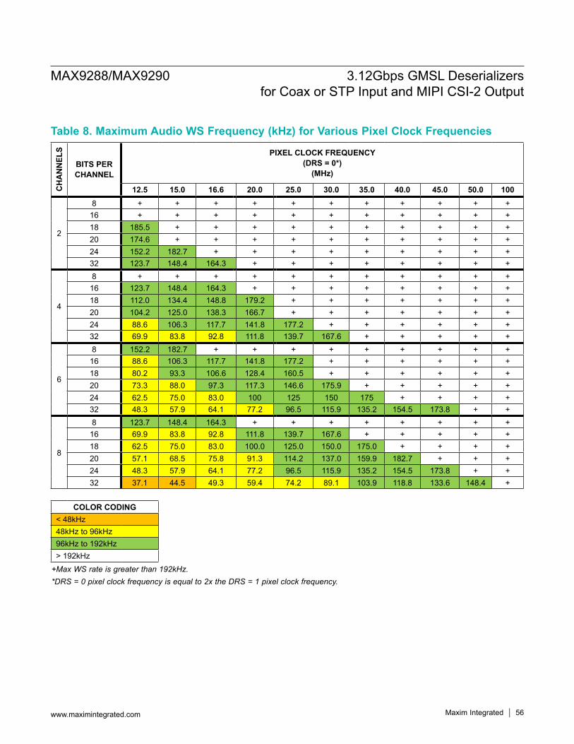
MAX9288/MAX9290 3.12Gbps GMSL Deserializers for Coax or STP Input and MIPI CSI-2 Output
www.maximintegrated.com Maxim Integrated 56
Table 8. Maximum Audio WS Frequency (kHz) for Various Pixel Clock Frequencies
+Max WS rate is greater than 192kHz.*DRS = 0 pixel clock frequency is equal to 2x the DRS = 1 pixel clock frequency.
CH
AN
NEL
S
BITS PER CHANNEL
PIXEL CLOCK FREQUENCY(DRS = 0*)
(MHz)
12.5 15.0 16.6 20.0 25.0 30.0 35.0 40.0 45.0 50.0 100
2
8 + + + + + + + + + + +16 + + + + + + + + + + +18 185.5 + + + + + + + + + +20 174.6 + + + + + + + + + +24 152.2 182.7 + + + + + + + + +32 123.7 148.4 164.3 + + + + + + + +
4
8 + + + + + + + + + + +16 123.7 148.4 164.3 + + + + + + + +18 112.0 134.4 148.8 179.2 + + + + + + +20 104.2 125.0 138.3 166.7 + + + + + + +24 88.6 106.3 117.7 141.8 177.2 + + + + + +32 69.9 83.8 92.8 111.8 139.7 167.6 + + + + +
6
8 152.2 182.7 + + + + + + + + +16 88.6 106.3 117.7 141.8 177.2 + + + + + +18 80.2 93.3 106.6 128.4 160.5 + + + + + +20 73.3 88.0 97.3 117.3 146.6 175.9 + + + + +24 62.5 75.0 83.0 100 125 150 175 + + + +32 48.3 57.9 64.1 77.2 96.5 115.9 135.2 154.5 173.8 + +
8
8 123.7 148.4 164.3 + + + + + + + +16 69.9 83.8 92.8 111.8 139.7 167.6 + + + + +18 62.5 75.0 83.0 100.0 125.0 150.0 175.0 + + + +20 57.1 68.5 75.8 91.3 114.2 137.0 159.9 182.7 + + +24 48.3 57.9 64.1 77.2 96.5 115.9 135.2 154.5 173.8 + +32 37.1 44.5 49.3 59.4 74.2 89.1 103.9 118.8 133.6 148.4 +
COLOR CODING< 48kHz48kHz to 96kHz96kHz to 192kHz> 192kHz
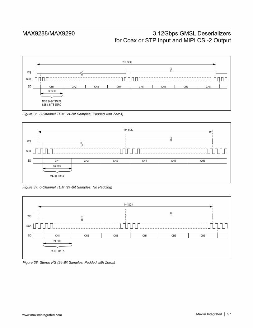
MAX9288/MAX9290 3.12Gbps GMSL Deserializers for Coax or STP Input and MIPI CSI-2 Output
www.maximintegrated.com Maxim Integrated 57
Figure 36. 8-Channel TDM (24-Bit Samples, Padded with Zeros)
Figure 37. 6-Channel TDM (24-Bit Samples, No Padding)
Figure 38. Stereo I2S (24-Bit Samples, Padded with Zeros)
WS
SCK
SD CH132 SCK
CH2 CH3 CH4 CH5
256 SCK
CH6 CH7 CH8
MSB 24-BIT DATALSB 8 BITS ZERO
WS
SCK
SD CH1 CH2 CH3 CH4 CH5 CH6
24 SCK
24-BIT DATA
144 SCK
WS
SCK
SD CH1 CH2 CH3 CH4 CH5 CH6
24 SCK
24-BIT DATA
144 SCK
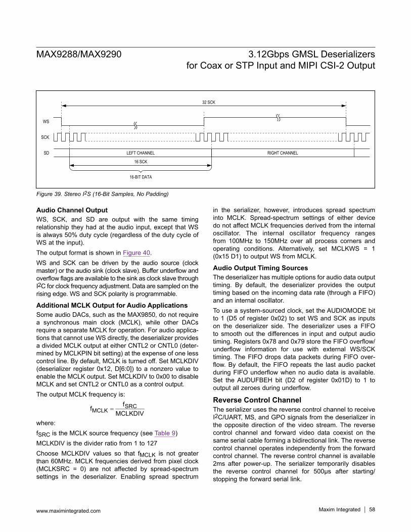
MAX9288/MAX9290 3.12Gbps GMSL Deserializers for Coax or STP Input and MIPI CSI-2 Output
www.maximintegrated.com Maxim Integrated 58
Audio Channel OutputWS, SCK, and SD are output with the same timing relationship they had at the audio input, except that WS is always 50% duty cycle (regardless of the duty cycle of WS at the input).The output format is shown in Figure 40.WS and SCK can be driven by the audio source (clock master) or the audio sink (clock slave). Buffer underflow and overflow flags are available to the sink as clock slave through I2C for clock frequency adjustment. Data are sampled on the rising edge. WS and SCK polarity is programmable.
Additional MCLK Output for Audio ApplicationsSome audio DACs, such as the MAX9850, do not require a synchronous main clock (MCLK), while other DACs require a separate MCLK for operation. For audio applica-tions that cannot use WS directly, the deserializer provides a divided MCLK output at either CNTL2 or CNTL0 (deter-mined by MCLKPIN bit setting) at the expense of one less control line. By default, MCLK is turned off. Set MCLKDIV (deserializer register 0x12, D[6:0]) to a nonzero value to enable the MCLK output. Set MCLKDIV to 0x00 to disable MCLK and set CNTL2 or CNTL0 as a control output.The output MCLK frequency is:
SRCMCLK
ffMCLKDIV
=
where:fSRC is the MCLK source frequency (see Table 9)MCLKDIV is the divider ratio from 1 to 127Choose MCLKDIV values so that fMCLK is not greater than 60MHz. MCLK frequencies derived from pixel clock (MCLKSRC = 0) are not affected by spread-spectrum settings in the deserializer. Enabling spread spectrum
in the serializer, however, introduces spread spectrum into MCLK. Spread-spectrum settings of either device do not affect MCLK frequencies derived from the internal oscillator. The internal oscillator frequency ranges from 100MHz to 150MHz over all process corners and operating conditions. Alternatively, set MCLKWS = 1 (0x15 D1) to output WS from MCLK.
Audio Output Timing SourcesThe deserializer has multiple options for audio data output timing. By default, the deserializer provides the output timing based on the incoming data rate (through a FIFO) and an internal oscillator.To use a system-sourced clock, set the AUDIOMODE bit to 1 (D5 of register 0x02) to set WS and SCK as inputs on the deserializer side. The deserializer uses a FIFO to smooth out the differences in input and output audio timing. Registers 0x78 and 0x79 store the FIFO overflow/underflow information for use with external WS/SCK timing. The FIFO drops data packets during FIFO over-flow. By default, the FIFO repeats the last audio packet during FIFO underflow when no audio data is available. Set the AUDUFBEH bit (D2 of register 0x01D) to 1 to output all zeroes during underflow.
Reverse Control ChannelThe serializer uses the reverse control channel to receive I2C/UART, MS, and GPO signals from the deserializer in the opposite direction of the video stream. The reverse control channel and forward video data coexist on the same serial cable forming a bidirectional link. The reverse control channel operates independently from the forward control channel. The reverse control channel is available 2ms after power-up. The serializer temporarily disables the reverse control channel for 500µs after starting/stopping the forward serial link.
Figure 39. Stereo I2S (16-Bit Samples, No Padding)
32 SCK
LEFT CHANNEL RIGHT CHANNEL
16 SCK
16-BIT DATA
WS
SCK
SD
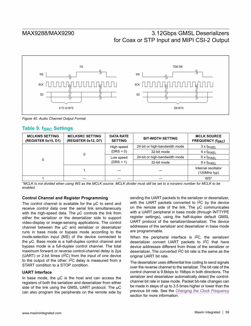
MAX9288/MAX9290 3.12Gbps GMSL Deserializers for Coax or STP Input and MIPI CSI-2 Output
www.maximintegrated.com Maxim Integrated 59
Control Channel and Register ProgrammingThe control channel is available for the µC to send and receive control data over the serial link simultaneously with the high-speed data. The µC controls the link from either the serializer or the deserializer side to support video-display or image-sensing applications. The control channel between the µC and serializer or deserializer runs in base mode or bypass mode according to the mode-selection input (MS) of the device connected to the µC. Base mode is a half-duplex control channel and bypass mode is a full-duplex control channel. The total maximum forward or reverse control-channel delay is 2µs (UART) or 2-bit times (I2C) from the input of one device to the output of the other. I2C delay is measured from a START condition to a STOP condition.
UART InterfaceIn base mode, the µC is the host and can access the registers of both the serializer and deserializer from either side of the link using the GMSL UART protocol. The µC can also program the peripherals on the remote side by
sending the UART packets to the serializer or deserializer, with the UART packets converted to I2C by the device on the remote side of the link. The µC communicates with a UART peripheral in base mode (through INTTYPE register settings), using the half-duplex default GMSL UART protocol of the serializer/deserializer. The device addresses of the serializer and deserializer in base mode are programmable.When the peripheral interface is I2C, the serializer/deserializer convert UART packets to I2C that have device addresses different from those of the serializer or deserializer. The converted I2C bit rate is the same as the original UART bit rate.The deserializer uses differential line coding to send signals over the reverse channel to the serializer. The bit rate of the control channel is 9.6kbps to 1Mbps in both directions. The serializer and deserializer automatically detect the control-channel bit rate in base mode. Packet bit-rate changes can be made in steps of up to 3.5 times higher or lower than the previous bit rate. See the Changing the Clock Frequency section for more information.
Table 9. fSRC Settings
*MCLK is not divided when using WS as the MCLK source. MCLK divider must still be set to a nonzero number for MCLK to be enabled.
Figure 40. Audio Channel Output Format
MCLKWS SETTING (REGISTER 0x15, D1)
MCLKSRC SETTING (REGISTER 0x12, D7)
DATA RATE SETTING BIT-WIDTH SETTING MCLK SOURCE
FREQUENCY (fSRC)
00
High speed(DRS = 0)
24-bit or high-bandwidth mode 3 x fPIXEL32-bit mode 4 x fPIXEL
Low speed(DRS = 1)
24-bit or high-bandwidth mode 6 x fPIXEL32-bit mode 8 x fPIXEL
1 — — Internal oscillator(120MHz typ)
1 — — — WS*
I2S TDM 256
SCK
SD
WS
SCK
SD
WS
8 TO 32 BITS 256 BITS
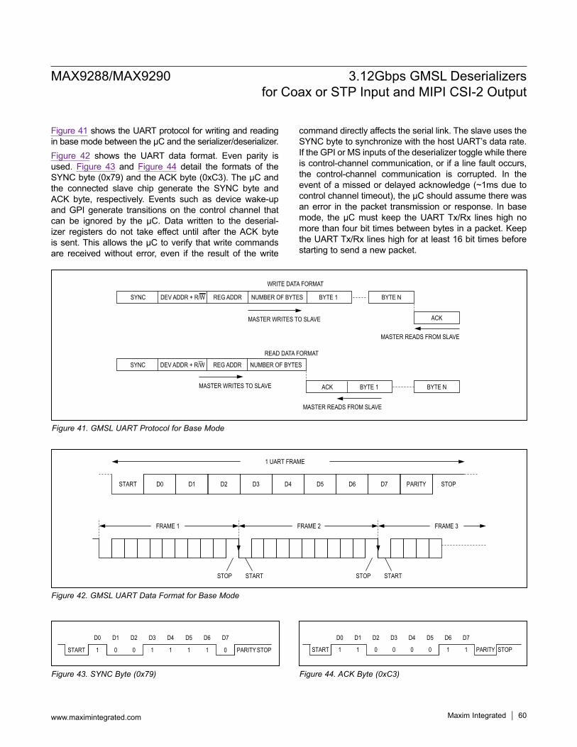
MAX9288/MAX9290 3.12Gbps GMSL Deserializers for Coax or STP Input and MIPI CSI-2 Output
www.maximintegrated.com Maxim Integrated 60
Figure 41 shows the UART protocol for writing and reading in base mode between the µC and the serializer/deserializer.Figure 42 shows the UART data format. Even parity is used. Figure 43 and Figure 44 detail the formats of the SYNC byte (0x79) and the ACK byte (0xC3). The µC and the connected slave chip generate the SYNC byte and ACK byte, respectively. Events such as device wake-up and GPI generate transitions on the control channel that can be ignored by the µC. Data written to the deserial-izer registers do not take effect until after the ACK byte is sent. This allows the µC to verify that write commands are received without error, even if the result of the write
command directly affects the serial link. The slave uses the SYNC byte to synchronize with the host UART’s data rate. If the GPI or MS inputs of the deserializer toggle while there is control-channel communication, or if a line fault occurs, the control-channel communication is corrupted. In the event of a missed or delayed acknowledge (~1ms due to control channel timeout), the µC should assume there was an error in the packet transmission or response. In base mode, the µC must keep the UART Tx/Rx lines high no more than four bit times between bytes in a packet. Keep the UART Tx/Rx lines high for at least 16 bit times before starting to send a new packet.
Figure 41. GMSL UART Protocol for Base Mode
Figure 42. GMSL UART Data Format for Base Mode
Figure 43. SYNC Byte (0x79) Figure 44. ACK Byte (0xC3)
WRITE DATA FORMAT
SYNC DEV ADDR + R/W REG ADDR NUMBER OF BYTES
SYNC DEV ADDR + R/W REG ADDR NUMBER OF BYTES BYTE 1 BYTE N
ACK
BYTE NBYTE 1ACK
MASTER READS FROM SLAVE
READ DATA FORMAT
MASTER WRITES TO SLAVE
MASTER WRITES TO SLAVE
MASTER READS FROM SLAVE
START D0 D1 D2 D3 D4 D5 D6 D7 PARITY STOP
1 UART FRAME
FRAME 1 FRAME 2 FRAME 3
STOP START STOP START
START
D0
1 0 0 1 1 1 1 0
D1 D2 D3 D4 D5 D6 D7
PARITY STOP START
D0
1 1 0 0 0 0 1 1
D1 D2 D3 D4 D5 D6 D7
PARITY STOP
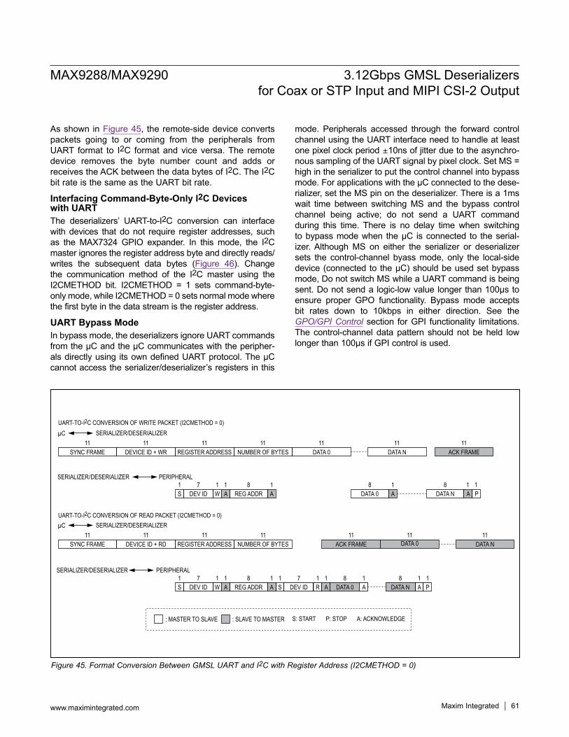
MAX9288/MAX9290 3.12Gbps GMSL Deserializers for Coax or STP Input and MIPI CSI-2 Output
www.maximintegrated.com Maxim Integrated 61
As shown in Figure 45, the remote-side device converts packets going to or coming from the peripherals from UART format to I2C format and vice versa. The remote device removes the byte number count and adds or receives the ACK between the data bytes of I2C. The I2C bit rate is the same as the UART bit rate.
Interfacing Command-Byte-Only I2C Devices with UARTThe deserializers’ UART-to-I2C conversion can interface with devices that do not require register addresses, such as the MAX7324 GPIO expander. In this mode, the I2C master ignores the register address byte and directly reads/writes the subsequent data bytes (Figure 46). Change the communication method of the I2C master using the I2CMETHOD bit. I2CMETHOD = 1 sets command-byte-only mode, while I2CMETHOD = 0 sets normal mode where the first byte in the data stream is the register address.
UART Bypass ModeIn bypass mode, the deserializers ignore UART commands from the µC and the µC communicates with the peripher-als directly using its own defined UART protocol. The µC cannot access the serializer/deserializer’s registers in this
mode. Peripherals accessed through the forward control channel using the UART interface need to handle at least one pixel clock period ±10ns of jitter due to the asynchro-nous sampling of the UART signal by pixel clock. Set MS = high in the serializer to put the control channel into bypass mode. For applications with the µC connected to the dese-rializer, set the MS pin on the deserializer. There is a 1ms wait time between switching MS and the bypass control channel being active; do not send a UART command during this time. There is no delay time when switching to bypass mode when the µC is connected to the serial-izer. Although MS on either the serializer or deserializer sets the control-channel byass mode, only the local-side device (connected to the µC) should be used set bypass mode, Do not switch MS while a UART command is being sent. Do not send a logic-low value longer than 100µs to ensure proper GPO functionality. Bypass mode accepts bit rates down to 10kbps in either direction. See the GPO/GPI Control section for GPI functionality limitations. The control-channel data pattern should not be held low longer than 100µs if GPI control is used.
Figure 45. Format Conversion Between GMSL UART and I2C with Register Address (I2CMETHOD = 0)
11SYNC FRAME REGISTER ADDRESS NUMBER OF BYTESDEVICE ID + WR DATA 0
DEV ID A
11 11 11 11DATA N
11 11
S1 11
ACK FRAME
7
: MASTER TO SLAVE
8
SERIALIZER/DESERIALIZER PERIPHERAL
W1
REG ADDR8
A1 1 8 1
11SYNC FRAME REGISTER ADDRESS NUMBER OF BYTESDEVICE ID + RD
11 11 11 11ACK FRAME DATA 0
11DATA N
11
UART-TO-I2C CONVERSION OF WRITE PACKET (I2CMETHOD = 0)
UART-TO-I2C CONVERSION OF READ PACKET (I2CMETHOD = 0)
S: START P: STOP A: ACKNOWLEDGE: SLAVE TO MASTER
DATA 0 A DATA N A P
DEV ID AS1 17
W1
DEV ID AS1 17
R1
DATA N P18
A1
DATA 08
A1
REG ADDR8
A1
µC SERIALIZER/DESERIALIZER
µC SERIALIZER/DESERIALIZER
SERIALIZER/DESERIALIZER PERIPHERAL
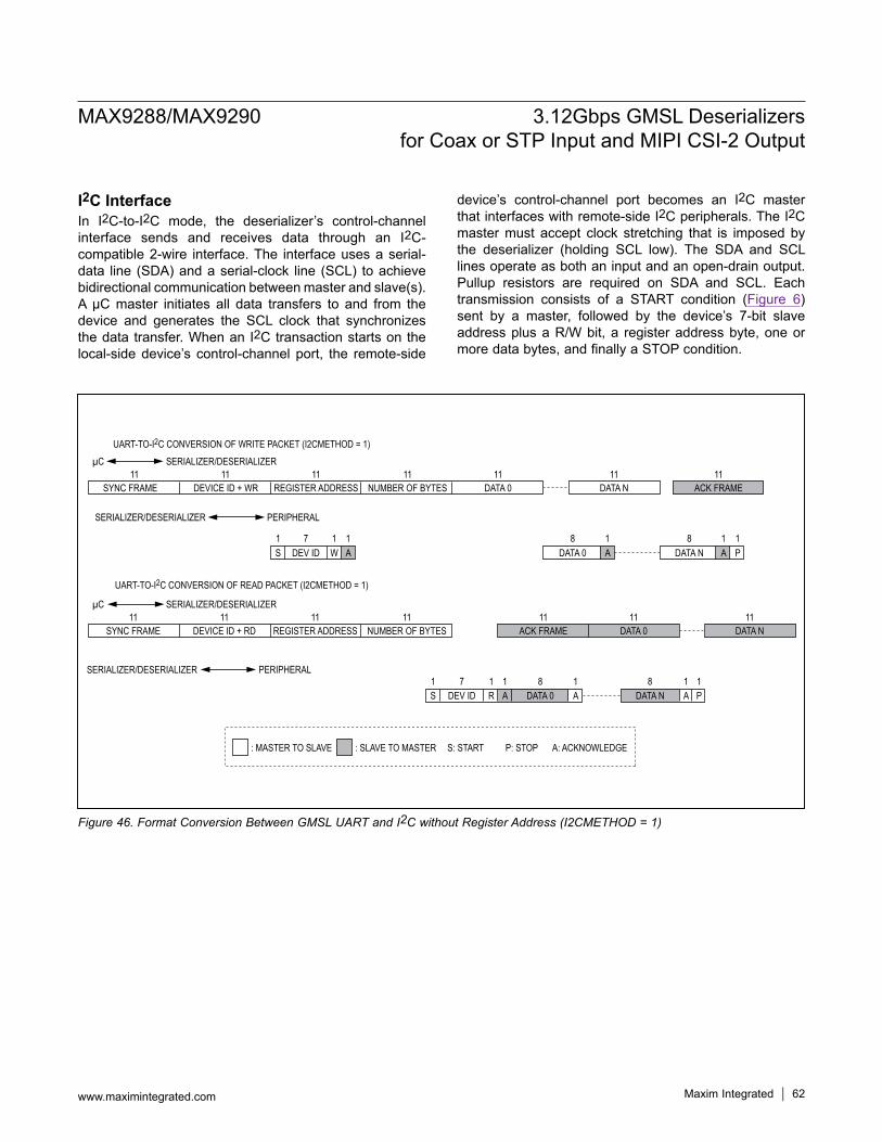
MAX9288/MAX9290 3.12Gbps GMSL Deserializers for Coax or STP Input and MIPI CSI-2 Output
www.maximintegrated.com Maxim Integrated 62
I2C InterfaceIn I2C-to-I2C mode, the deserializer’s control-channel interface sends and receives data through an I2C-compatible 2-wire interface. The interface uses a serial-data line (SDA) and a serial-clock line (SCL) to achieve bidirectional communication between master and slave(s). A µC master initiates all data transfers to and from the device and generates the SCL clock that synchronizes the data transfer. When an I2C transaction starts on the local-side device’s control-channel port, the remote-side
device’s control-channel port becomes an I2C master that interfaces with remote-side I2C peripherals. The I2C master must accept clock stretching that is imposed by the deserializer (holding SCL low). The SDA and SCL lines operate as both an input and an open-drain output. Pullup resistors are required on SDA and SCL. Each transmission consists of a START condition (Figure 6) sent by a master, followed by the device’s 7-bit slave address plus a R/W bit, a register address byte, one or more data bytes, and finally a STOP condition.
Figure 46. Format Conversion Between GMSL UART and I2C without Register Address (I2CMETHOD = 1)
: MASTER TO SLAVE
SERIALIZER/DESERIALIZER
SERIALIZER/DESERIALIZER
SERIALIZER/DESERIALIZER
UART-TO-I2C CONVERSION OF READ PACKET (I2CMETHOD = 1)
UART-TO-I2C CONVERSION OF WRITE PACKET (I2CMETHOD = 1)
µC
SERIALIZER/DESERIALIZERµC
SYNC FRAME
11 11 11 11 11 11 11
1111 11 11 11 11 11DEVICE ID + RD REGISTER ADDRESS NUMBER OF BYTES
SYNC FRAME DEVICE ID + WR REGISTER ADDRESS NUMBER OF BYTES DATA 0 DATA N ACK FRAME
ACK FRAME DATA 0 DATA N
DATA NADATA 0W ADEV IDS A P
PERIPHERAL
PERIPHERAL
S1 1 1 8
8 81111 7 1 1
81 1 17DEV ID R A A A PDATA 0 DATA N
: SLAVE TO MASTER S: START P: STOP A: ACKNOWLEDGE
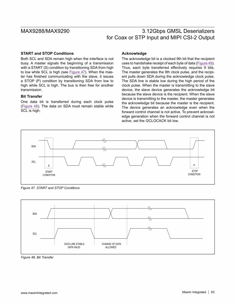
MAX9288/MAX9290 3.12Gbps GMSL Deserializers for Coax or STP Input and MIPI CSI-2 Output
www.maximintegrated.com Maxim Integrated 63
START and STOP ConditionsBoth SCL and SDA remain high when the interface is not busy. A master signals the beginning of a transmission with a START (S) condition by transitioning SDA from high to low while SCL is high (see Figure 47). When the mas-ter has finished communicating with the slave, it issues a STOP (P) condition by transitioning SDA from low to high while SCL is high. The bus is then free for another transmission.
Bit TransferOne data bit is transferred during each clock pulse (Figure 48). The data on SDA must remain stable while SCL is high.
AcknowledgeThe acknowledge bit is a clocked 9th bit that the recipient uses to handshake receipt of each byte of data (Figure 49). Thus, each byte transferred effectively requires 9 bits. The master generates the 9th clock pulse, and the recipi-ent pulls down SDA during the acknowledge clock pulse. The SDA line is stable low during the high period of the clock pulse. When the master is transmitting to the slave device, the slave device generates the acknowledge bit because the slave device is the recipient. When the slave device is transmitting to the master, the master generates the acknowledge bit because the master is the recipient. The device generates an acknowledge even when the forward control channel is not active. To prevent acknowl-edge generation when the forward control channel is not active, set the I2CLOCACK bit low.
Figure 47. START and STOP Conditions
Figure 48. Bit Transfer
SDA
SCL
START CONDITION
STOPCONDITION
S P
SDA
SCL
DATA LINE STABLE;DATA VALID
CHANGE OF DATAALLOWED
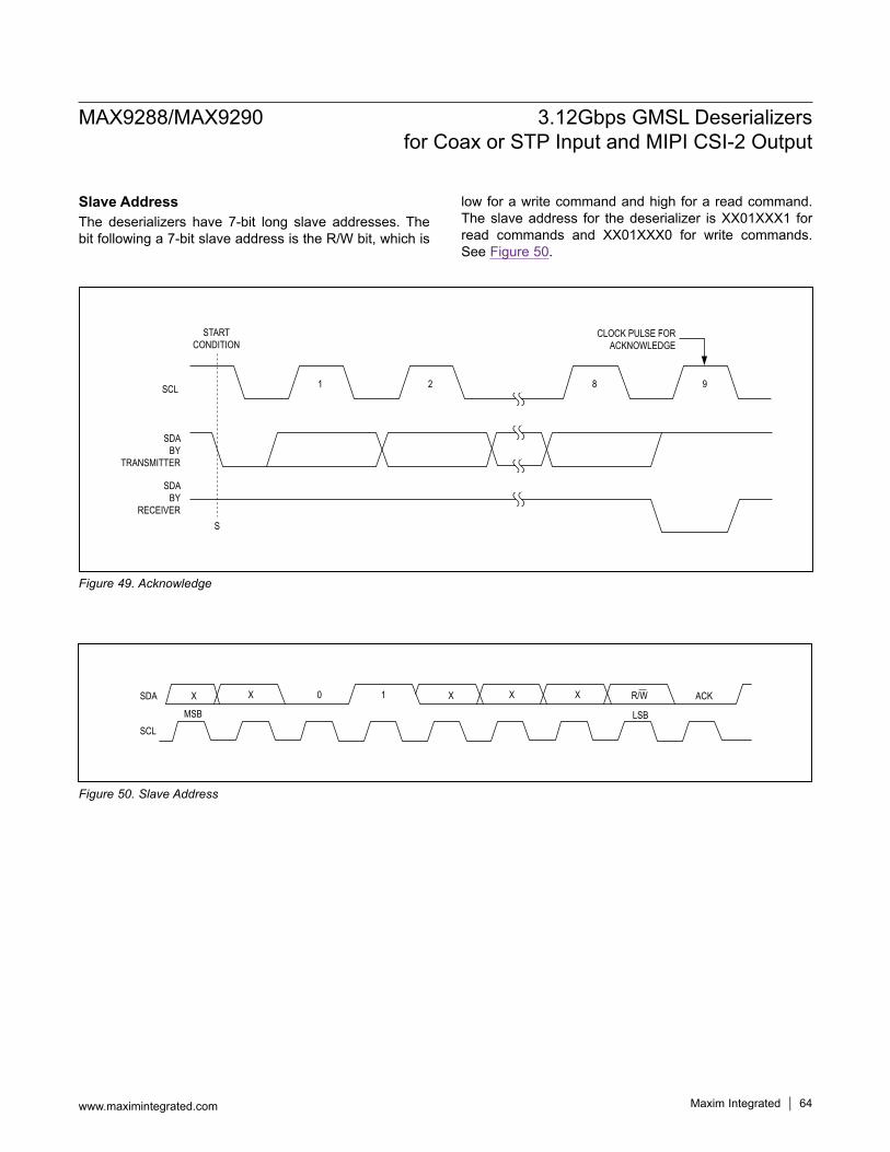
MAX9288/MAX9290 3.12Gbps GMSL Deserializers for Coax or STP Input and MIPI CSI-2 Output
www.maximintegrated.com Maxim Integrated 64
Slave AddressThe deserializers have 7-bit long slave addresses. The bit following a 7-bit slave address is the R/W bit, which is
low for a write command and high for a read command. The slave address for the deserializer is XX01XXX1 for read commands and XX01XXX0 for write commands. See Figure 50.
Figure 49. Acknowledge
Figure 50. Slave Address
SCL
SDABY
TRANSMITTER
CLOCK PULSE FORACKNOWLEDGE
START CONDITION
SDABY
RECEIVER
1 2 8 9
S
SDA X ACK
SCLMSB LSB
X X R/W0 1 X X
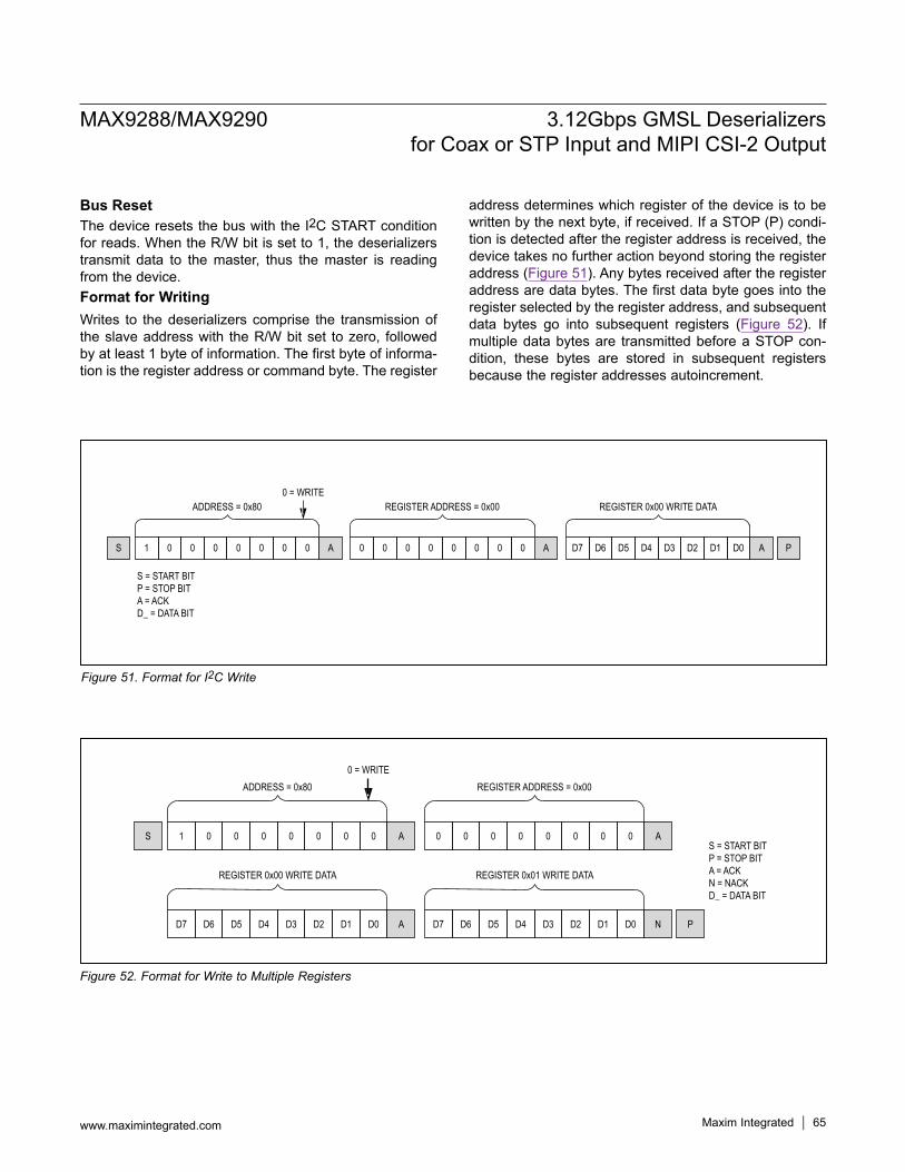
MAX9288/MAX9290 3.12Gbps GMSL Deserializers for Coax or STP Input and MIPI CSI-2 Output
www.maximintegrated.com Maxim Integrated 65
Bus ResetThe device resets the bus with the I2C START condition for reads. When the R/W bit is set to 1, the deserializers transmit data to the master, thus the master is reading from the device.Format for WritingWrites to the deserializers comprise the transmission of the slave address with the R/W bit set to zero, followed by at least 1 byte of information. The first byte of informa-tion is the register address or command byte. The register
address determines which register of the device is to be written by the next byte, if received. If a STOP (P) condi-tion is detected after the register address is received, the device takes no further action beyond storing the register address (Figure 51). Any bytes received after the register address are data bytes. The first data byte goes into the register selected by the register address, and subsequent data bytes go into subsequent registers (Figure 52). If multiple data bytes are transmitted before a STOP con-dition, these bytes are stored in subsequent registers because the register addresses autoincrement.
Figure 51. Format for I2C Write
Figure 52. Format for Write to Multiple Registers
S 1 0 0 0
ADDRESS = 0x800 = WRITE
0 0 0 0 A 0 0 0 0
REGISTER ADDRESS = 0x00
0 0 0 0 A PD7 D6 D5 D4
REGISTER 0x00 WRITE DATA
D3 D2 D1 D0 A
S = START BITP = STOP BITA = ACKD_ = DATA BIT
S = START BITP = STOP BITA = ACKN = NACKD_ = DATA BIT
S 1 0 0 0
ADDRESS = 0x800 = WRITE
0 0 0 0 A 0 0 0 0
REGISTER ADDRESS = 0x00
0 0 0 0 A
D7 D6 D5 D4
REGISTER 0x00 WRITE DATA
D3 D2 D1 D0 A D7 PD6 D5 D4
REGISTER 0x01 WRITE DATA
D3 D2 D1 D0 N
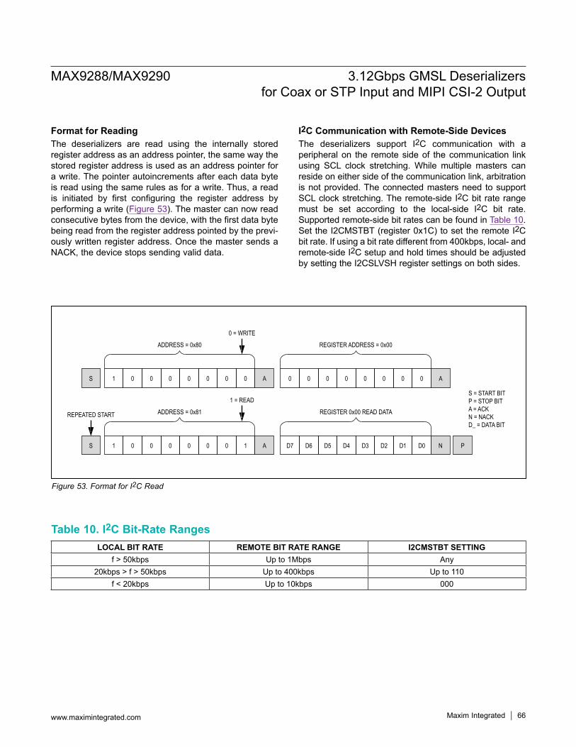
MAX9288/MAX9290 3.12Gbps GMSL Deserializers for Coax or STP Input and MIPI CSI-2 Output
www.maximintegrated.com Maxim Integrated 66
Format for ReadingThe deserializers are read using the internally stored register address as an address pointer, the same way the stored register address is used as an address pointer for a write. The pointer autoincrements after each data byte is read using the same rules as for a write. Thus, a read is initiated by first configuring the register address by performing a write (Figure 53). The master can now read consecutive bytes from the device, with the first data byte being read from the register address pointed by the previ-ously written register address. Once the master sends a NACK, the device stops sending valid data.
I2C Communication with Remote-Side DevicesThe deserializers support I2C communication with a peripheral on the remote side of the communication link using SCL clock stretching. While multiple masters can reside on either side of the communication link, arbitration is not provided. The connected masters need to support SCL clock stretching. The remote-side I2C bit rate range must be set according to the local-side I2C bit rate. Supported remote-side bit rates can be found in Table 10. Set the I2CMSTBT (register 0x1C) to set the remote I2C bit rate. If using a bit rate different from 400kbps, local- and remote-side I2C setup and hold times should be adjusted by setting the I2CSLVSH register settings on both sides.
Figure 53. Format for I2C Read
Table 10. I2C Bit-Rate RangesLOCAL BIT RATE REMOTE BIT RATE RANGE I2CMSTBT SETTING
f > 50kbps Up to 1Mbps Any20kbps > f > 50kbps Up to 400kbps Up to 110
f < 20kbps Up to 10kbps 000
S = START BITP = STOP BITA = ACKN = NACKD_ = DATA BIT
S
S
1 0 0 0
ADDRESS = 0x80
0 = WRITE
0 0 0 0 A
1 = READ
REPEATED START
0 0 0 0
REGISTER ADDRESS = 0x00
0 0 0 0 A
1 0 0 0
ADDRESS = 0x81
0 0 0 1 A D7 PD6 D5 D4
REGISTER 0x00 READ DATA
D3 D2 D1 D0 N
MAX9288/MAX9290 3.12Gbps GMSL Deserializers for Coax or STP Input and MIPI CSI-2 Output
www.maximintegrated.com Maxim Integrated 67
I2C Address TranslationThe deserializers support I2C address translation for up to two device addresses. Use address translation to assign unique device addresses to peripherals with limited I2C addresses. Source addresses (address to translate from) are stored in registers 0x18 and 0x1A. Destination addresses (address to translate to) are stored in registers 0x19 and 0x1B.In a multilink situation where there are multiple deserial-izers and/or peripheral devices connected to these serial-izers, the deserializers support broadcast commands to control these multiple devices. Select an unused device address to use as a broadcast device address. Program all the remote-side serializer devices to translate the broadcast device address (source address stored in reg-isters 0x0F, 0x11) to the peripherals’ address (destination address stored in registers 0x10, 0x12). Any commands sent to the broadcast address (selected unused address) are sent to all deserializers and/or peripheral devices con-nected to the deserializers whose addresses match the translated broadcast address.
GPO/GPI ControlGPO on the serializer follows GPI transitions on the dese-rializer. This GPO/GPI function can be used to transmit signals such as a frame sync in a surround-view camera system. The GPI-to-GPO delay is 0.35ms max. Keep time between GPI transitions to a minimum 0.35ms. This includes transitions from the other deserializer in coax splitter mode. Bit D4 of register 0x06 in the deserializer stores the GPI input state. GPO is low after power-up. The µC can set GPO by writing to the SETGPO register bit. Do not send a logic-low value on the deserializer RX/SDA input (UART mode) longer than 100µs in either base or bypass mode to ensure proper GPO/GPI functionality. GPO/GPI commands will override and cor-rupt an I2C/UART command in progress.
Line EqualizerThe deserializer includes an adjustable line equalizer to further compensate cable attenuation at high frequencies. The cable equalizer has 11 selectable levels of compen-sation from 2.1dB to 13dB (Table 11). To select other equalization levels, set the corresponding register bits in the deserializer (0x05 D[3:0]). Use equalization in the
deserializer, together with preemphasis in the serializer, to create the most reliable link for a given cable.
HS/VS/DE TrackingThe deserializer has tracking to filter out HS/VS/DE bit or packet errors. HS/VS/DE tracking is on by default when the device is in high-bandwidth mode (BWS = open), and off by default when in 24-bit or 32-bit mode (BWS = low or high). Set/clear HVTREN (D6 of register 0x15) to enable/disable HS/VS tracking. Set/clear DETREN (D5 of register 0x15) to enable/disable DE tracking. By default, the device uses a partial and full periodic tracking of HS/DE. Set HVTRMODE = 0 (D4 of register 0x15) to disable full periodic tracking. HS/VS/DE tracking can be turned on in 24-bit and 32-bit modes to track and correct against bit errors in HS/VS/DE link bits.
Serial InputThe device can receive serial data from two kinds of cable: 100Ω twisted pair and 50Ω coax. (Contact the factory for devices compatible with 75Ω cables).
Table 11. Cable Equalizer Boost LevelsBOOST SETTING
(0x05 D[3:0]) TYPICAL BOOST GAIN (dB)
0000 2.10001 2.80010 3.40011 4.2
01005.2
Power-up default when EQS is set high
0101 6.20110 70111 8.21000 9.4
100110.7
Power-up default when EQS is set low
1010 11.71011 13
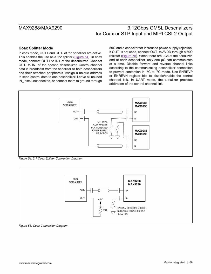
MAX9288/MAX9290 3.12Gbps GMSL Deserializers for Coax or STP Input and MIPI CSI-2 Output
www.maximintegrated.com Maxim Integrated 68
Coax Splitter ModeIn coax mode, OUT+ and OUT- of the serializer are active. This enables the use as a 1:2 splitter (Figure 54). In coax mode, connect OUT+ to IN+ of the deserializer. Connect OUT- to IN- of the second deserializer. Control-channel data is broadcast from the serializer to both deserializers and their attached peripherals. Assign a unique address to send control data to one deserializer. Leave all unused IN_ pins unconnected, or connect them to ground through
50Ω and a capacitor for increased power-supply rejection. If OUT- is not used, connect OUT- to AVDD through a 50Ω resistor (Figure 55). When there are µCs at the serializer, and at each deserializer, only one µC can communicate at a time. Disable forward and reverse channel links according to the communicating deserializer connection to prevent contention in I2C-to-I2C mode. Use ENREVP or ENREVN register bits to disable/enable the control channel link. In UART mode, the serializer provides arbitration of the control-channel link.
Figure 54. 2:1 Coax Splitter Connection Diagram
Figure 55. Coax Connection Diagram
OUT+
OUT-OPTIONAL
COMPONENTSFOR INCREASEDPOWER-SUPPLY
REJECTION
IN+
IN-
IN+
IN-
MAX9288MAX9290
MAX9288MAX9290
GMSLSERIALIZER
OUT+
OUT-
IN+
OPTIONAL COMPONENTS FORINCREASED POWER-SUPPLYREJECTION
IN-AVDD
50Ω
MAX9288MAX9290
GMSLSERIALIZER
MAX9288/MAX9290 3.12Gbps GMSL Deserializers for Coax or STP Input and MIPI CSI-2 Output
www.maximintegrated.com Maxim Integrated 69
Cable Type Configuration InputCX/TP determine the power-up state of the serial input. In coax mode, CX/TP also determine which coax input is active, along with the default device address (Table 12).
Color Lookup TablesThe deserializer includes three color lookup tables (LUT) to support automatic translation of pixel values. The LUT can be used for RGB666, RGB888, and user-defined generic 8-bit CSI-2 outputs. This feature can be used for color gamma correction, brightness/contrast or for other purposes. There are three lookup tables, each 8 bits wide and 256 entries deep, enabling a 1-to-1 translation of 8-bit input values to any 8-bit output value for each color (24 bits total).
Programming and Verifying LUT DataThe µC must set the LUTPROG register bit to 1 before programming and verifying the tables. To program a LUT, the µC generates a write packet with register address set to the assigned register address for respective LUT (0x7D, 0x7E, or 0x7F). The deserializer writes data in the packet to the respective LUT starting from the LUT address location set in the LUTADDR register. Successive bytes in the data packet are written to the next LUT address location; however, each new data-packet write starts from
the address location stored in the LUTADDR register. Use 0x00 for LUTADDR and 0x00 as the number of bytes field in UART packet, when writing a 256-byte data block, because 8-bit-wide number of bytes field cannot normally represent 9-bit wide “256” value. There is no number of bytes field in I2C-to-I2C modes.To read back the contents of an LUT, the µC generates a read packet with register address set to the assigned register address for respective LUT (0x7D, 0x7E, or 0x7F). The deserializer outputs read data from the respective LUT starting from the LUT address location set in the LUT_ADDR register. Similar to the write operation, use 0x00 for LUTADDR and 0x00 as the number of bytes field in UART packet, when reading a 256-byte data block.
LUT Color TranslationAfter power-up or going out of sleep or power-down modes, LUT translation is disabled and LUT contents are unknown. After program and verify operations are finished, in order to enable LUT translations, set the LUTPROG bit to 0 and set the respective LUT enable bits (RED_LUT_EN, GRN_LUT_EN, BLU_LUT_EN) to 1 to enable the desired LUT translation function. Only the selected colors are translated by the LUT (the other colors are not touched). The µC does not need to fill in all three color lookup tables if all three color translations are not needed.After a pixel is deserialized, decoded, and decrypted (if necessary), it is segmented into its color components red, green, and blue (RGB) according to Table 13 and Figure 56. If LUT translation is enabled, each 8-bit pretranslation color value is used as address to the respective LUT table to look up the corresponding (translated) 8-bit color value.
Table 13. Pixel Data Format
Table 12. Configuration Input MapCX/TP FUNCTIONHigh Coax+ input. 7-bit device address is XXXXXX0 (bin).Mid Coax- input. 7-bit device address is XXXXXX1 (bin).
Low Twisted-pair input. 7-bit device address is XXXXXX0 (bin).
DOUT [5:0]
DOUT [11:6]
DOUT [17:12] DOUT18 DOUT19 DOUT20 DOUT
[22:21]DOUT [24:23]
DOUT [26:25]
R[5:0] G[5:0] B[5:0] HS VS DE R[7:6] G[7:6] B[7:6]
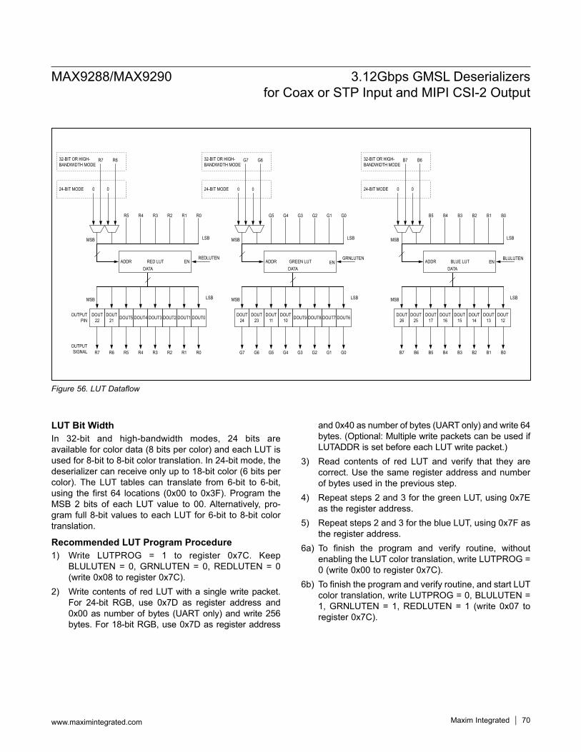
MAX9288/MAX9290 3.12Gbps GMSL Deserializers for Coax or STP Input and MIPI CSI-2 Output
www.maximintegrated.com Maxim Integrated 70
LUT Bit WidthIn 32-bit and high-bandwidth modes, 24 bits are available for color data (8 bits per color) and each LUT is used for 8-bit to 8-bit color translation. In 24-bit mode, the deserializer can receive only up to 18-bit color (6 bits per color). The LUT tables can translate from 6-bit to 6-bit, using the first 64 locations (0x00 to 0x3F). Program the MSB 2 bits of each LUT value to 00. Alternatively, pro-gram full 8-bit values to each LUT for 6-bit to 8-bit color translation.
Recommended LUT Program Procedure1) Write LUTPROG = 1 to register 0x7C. Keep
BLULUTEN = 0, GRNLUTEN = 0, REDLUTEN = 0 (write 0x08 to register 0x7C).
2) Write contents of red LUT with a single write packet. For 24-bit RGB, use 0x7D as register address and 0x00 as number of bytes (UART only) and write 256 bytes. For 18-bit RGB, use 0x7D as register address
and 0x40 as number of bytes (UART only) and write 64 bytes. (Optional: Multiple write packets can be used if LUTADDR is set before each LUT write packet.)
3) Read contents of red LUT and verify that they are correct. Use the same register address and number of bytes used in the previous step.
4) Repeat steps 2 and 3 for the green LUT, using 0x7E as the register address.
5) Repeat steps 2 and 3 for the blue LUT, using 0x7F as the register address.
6a) To finish the program and verify routine, without enabling the LUT color translation, write LUTPROG = 0 (write 0x00 to register 0x7C).
6b) To finish the program and verify routine, and start LUT color translation, write LUTPROG = 0, BLULUTEN = 1, GRNLUTEN = 1, REDLUTEN = 1 (write 0x07 to register 0x7C).
Figure 56. LUT Dataflow
ADDR
R5 R4 R3 R2 R1 R0
24-BIT MODE
32-BIT OR HIGH-BANDWIDTH MODE
R7 R6
0 0
RED LUTDATA
MSB LSB
MSB LSB
DOUT3 DOUT9 DOUT8 DOUT7 DOUT6DOUT2 DOUT1 DOUT0DOUT4DOUT5
R5 R4 R3 R2 R1 R0R6R7
ADDR
G5 G4 G3 G2 G1 G0
G7 G6
0 0
GREEN LUTDATA
MSB LSB
MSB LSB
G5 G4 G3 G2 G1 G0G6G7
ADDR
B5 B4 B3 B2 B1 B0
B7 B6
0 0
BLUE LUTDATA
MSB LSB
MSB LSB
B5 B4 B3 B2 B1 B0B6B7
ENREDLUTEN
ENGRNLUTEN
ENBLULUTEN
DOUT22
DOUT24
DOUT26
DOUT25
DOUT17
DOUT16
DOUT15
DOUT14
DOUT13
DOUT12
DOUT23
DOUT11
DOUT10
DOUT21
OUTPUTPIN
OUTPUTSIGNAL
24-BIT MODE
32-BIT OR HIGH-BANDWIDTH MODE
24-BIT MODE
32-BIT OR HIGH-BANDWIDTH MODE
MAX9288/MAX9290 3.12Gbps GMSL Deserializers for Coax or STP Input and MIPI CSI-2 Output
www.maximintegrated.com Maxim Integrated 71
High-Immunity Reverse Control-Channel ModeThe deserializer contains a high-immunity reverse control-channel mode, which has increased robustness at half the bit rate over the standard GMSL reverse control-channel link (Table 14). Set HIM on the serializer and deserializer to use high-immunity mode at power-up. Set the HIGHIMM bit high in both the serializer and dese-rializer to enable high-immunity mode at any time after power-up. Set the HIGHIMM bit low in both the serializer and deserializer to use the legacy reverse control-channel mode. The deserializer reverse channel mode is not avail-able for 500µs/1.92ms after the reverse control-channel mode is changed through the serializer/deserializer’s HIGHIMM bit setting, respectively. The user must set HIM or the HIGHIMM bits to the same value for proper reverse control-channel communication.In high-immunity mode, Set HPFTUNE = 00 in the equal-izer, if the serial bit rate = [pixel clock x 30 (BWS = low or open) or 40 (BWS = high)] is larger than 1Gbps when BWS is low or high. When BWS = open, set HPFTUNE = 00 when the serial bit rate is larger than 2GBps. In addi-tion, use 47nF AC-coupling capacitors. Note that legacy reverse control-channel mode may not function when using 47nF AC-coupling capacitors.By default, high-immunity mode uses a 500kbps bit rate. Set REVFAST =1 (D7 in register 0x1A in the serializer and register 0x11 in the deserializer) in both devices to use a 1Mbps bit rate. Certain limitations apply when using the fast high-immunity mode (Table 15).
Sleep ModeThe deserializers have sleep mode to reduce power consumption. The devices enter or exit sleep mode by a command from a remote µC using the control channel. Set the SLEEP bit to 1 to initiate sleep mode. Entering sleep mode resets the HDCP registers, but not the con-figuration registers. The deserializer sleeps after serial link inactivity or 8ms (whichever arrives first) after setting its SLEEP = 1. See the Link Startup Procedure section for details on waking up the device for different µC and starting conditions.To wake up from the local side, send an arbitrary control-channel command to the deserializer, wait for 5ms for the chip to power up, and then write 0 to SLEEP register bit to make the wake-up permanent. To wake up from the remote side, enable serialization. The deserializer detects the activity on serial link and then when it locks, it auto-matically sets its SLEEP register bit to 0.
Power-Down ModeThe deserializers have a power-down mode that further reduces power consumption compared to sleep mode. Set PWDN low to enter power-down mode. In power-down, the parallel outputs remain high impedance. Entering power-down resets the device’s registers. Upon exiting power-down, the state of external pins ADD0–ADD2, CX/TP, I2CSEL, DRS, EQS, HIM/CNTL1, and BWS are latched.
Table 14. Reverse Control-Channel Modes
Table 15. Fast High-Immunity Mode Requirements
Fast high-immunity mode requires DRS = 0.
X = Don’t care.
HIGHIMM BIT OR SD/HIM PIN SETTING
REVFAST BIT REVERSE CONTROL-CHANNEL MODE
MAX UART/I2C BIT RATE
(kbps)
Low (0) X Legacy reverse control-channel mode (compatible with all GMSL devices) 1000
High (1)0 High-immunity mode 5001 Fast high-immunity mode 1000
BWS SETTING ALLOWED PIXEL CLOCK FREQUENCY (MHz)Low > 41.66High > 30Open > 83.33
MAX9288/MAX9290 3.12Gbps GMSL Deserializers for Coax or STP Input and MIPI CSI-2 Output
www.maximintegrated.com Maxim Integrated 72
Configuration LinkThe control channel can operate in a low-speed mode called configuration link in the absence of a clock input. This allows a microprocessor to program configuration registers before starting the video link. An internal oscil-lator provides the clock for the configuration link. Set CLINKEN = 1 on the serializer to enable configuration link. Configuration link is active until the video link is
enabled. The video link overrides the configuration link and attempts to lock when SEREN = 1.
Link Startup ProcedureTable 16 lists the startup procedure for image-sensing applications. The control channel is available after the video link or the configuration link is established. If the deserializer powers up after the serializer, the control channel becomes unavailable for 2ms after power-up.
Table 16. Startup Procedure for Image-Sensing Applications (CDS = High, Figure 58)
NO. µCSERIALIZER
DESERIALIZER(AUTOSTART ENABLED) (AUTOSTART DISABLED)
— µC connected to deserializer. Sets all configuration inputs.
Sets all configuration inputs.
Sets all configuration inputs.
1 Powers up.
Powers up and loads default settings. Establishes video link when valid PCLK available.
Powers up and loads default settings. Goes to sleep after 8ms.
Powers up and loads default settings. Locks to video link signal if available.
2 Writes deserializer configuration bits and gets an acknowledge.
Configuration changed from default settings.
3
Wakes up the serializer by sending dummy packet, and then writing SLEEP = 0 within 8ms. May not get an acknowledge (or gets a dummy acknowledge) if not locked.
Wakes up.
4Writes serializer configuration bits. May not get an acknowledge (or gets a dummy acknowledge) if not locked.
Configuration changed from default settings.
5If not already enabled, sets SEREN = 1, gets an acknowledge and waits for serial link to be established (~3ms).
Establishes video link when valid PCLK available (if not already enabled).
Locks to video link signal (if not already locked).
6 Begin sending video data to input. Video data serialized and sent across serial link. Video data received and deserialized.
MAX9288/MAX9290 3.12Gbps GMSL Deserializers for Coax or STP Input and MIPI CSI-2 Output
www.maximintegrated.com Maxim Integrated 73
High-Bandwidth Digital Content Protection (HDCP)Note: The explanation of HDCP operation in this data sheet is provided as a guide for general understanding. Implementation of HDCP in a product must meet the requirements given in the HDCP System v1.3 Amendment for GMSL, which is available from DCP.HDCP has two main phases of operation, authentication and the link integrity check. The µC starts authentica-tion by writing to the START_AUTHENTICATION bit in the GMSL serializer. The GMSL serializer generates a 64-bit random number. The host µC first reads the 64-bit random number from the GMSL serializer and writes it to the deserializer. The µC then reads the GMSL serial-izer public key selection vector (AKSV) and writes it to the deserializer. The µC then reads the deserializer KSV (BKSV) and writes it to the GMSL serializer. The µC begins checking BKSV against the revocation list. Using the cipher, the GMSL serializer and deserializer calculate a 16-bit response value, R0 and R0’, respectively. The GMSL amendment for HDCP reduces the 100ms mini-mum wait time allowed for the receiver to generate R0’ (specified in HDCP rev 1.3) to 128 pixel clock cycles in the GMSL amendment.There are two response-value comparison modes, internal comparison and µC comparison. Set EN_INT_COMP = 1 to select internal comparison mode. Set EN_INT_COMP = 0 to select µC comparison mode. In internal compari-son mode, the µC reads the deserializer response R0’ and writes it to the GMSL serializer. The GMSL serializer compares R0’ to its internally generated response value R0, and sets R0_RI_MATCHED. In µC comparison mode, the µC reads and compares the R0/R0’ values from the GMSL serializer/deserializer.During response-value generation and comparison, the host µC checks for a valid BKSV (having 20 1s and 20 0s is also reported in BKSV_INVALID) and checks BKSV against the revocation list. If BKSV is not on the list and the response values match, the host authenticates the link. If the response values do not match, the µC resam-ples the response values (as described in HDCP rev 1.3, Appendix C). If resampling fails, the µC restarts authen-tication by setting the RESET_HDCP bit in the GMSL serializer. If BKSV appears on the revocation list, the host cannot transmit data that requires protection. The host knows when the link is authenticated and decides when to output data requiring protection. The µC performs a link integrity check every 128 frames or every 2s ±0.5s. The GMSL serializer/deserializer generate response values
every 128 frames. These values are compared internally (internal comparison mode) or can be compared in the host µC.In addition, the GMSL serializer/deserializer provide response values for the enhanced link verification. Enhanced link verification is an optional method of link verification for faster detection of loss-of-synchronization. For this option, the GMSL serializer and deserializer generate 8-bit enhanced link-verification response values (PJ and PJ’) every 16 frames. The host must detect three consecutive PJ/PJ’ mismatches before resampling.
Encryption EnableThe GMSL link transfers either encrypted or nonen-crypted data. To encrypt data, the host µC sets the encryption enable (ENCRYPTION_ENABLE) bit in both the GMSL serializer and deserializer. The µC must set ENCRYPTION_ENABLE in the same VSYNC cycle in both the GMSL serializer and deserializer (no internal VSYNC falling edges between the two writes). The same timing applies when clearing ENCRYPTION_ENABLE to disable encryption.Note: ENCRYPTION_ENABLE enables/disables encryp-tion on the GMSL irrespective of the content. To comply with HDCP, the µC must not allow content requiring encryption to cross the GMSL unencrypted.The µC must complete the authentication process before enabling encryption. In addition, encryption must be dis-abled before starting a new authentication session.
Synchronization of EncryptionThe video vertical sync (VSYNC) synchronizes the start of encryption. Once encryption has started, the GMSL generates a new encryption key for each frame and each line, with the internal falling edge of VSYNC and HSYNC. Rekeying is transparent to data and does not disrupt the encryption of video or audio data.
Repeater SupportThe GMSL serializer/deserializer include features to build an HDCP repeater. An HDCP repeater receives and decrypts HDCP content and then encrypts and transmits on one or more downstream links. A repeater can also use decrypted HDCP content (e.g., to display on a screen). To support HDCP repeater-authentication protocol, the deserializer has a REPEATER register bit. This register bit must be set to 1 by a µC (most likely on the repeater module). Both the GMSL serializer and deserializer use SHA-1 hash-value calculation over the assembled KSV lists. HDCP GMSL links support a maximum of 15 receiv-ers (total number including the ones in repeater modules).
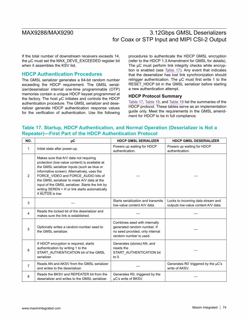
MAX9288/MAX9290 3.12Gbps GMSL Deserializers for Coax or STP Input and MIPI CSI-2 Output
www.maximintegrated.com Maxim Integrated 74
If the total number of downstream receivers exceeds 14, the µC must set the MAX_DEVS_EXCEEDED register bit when it assembles the KSV list.
HDCP Authentication ProceduresThe GMSL serializer generates a 64-bit random number exceeding the HDCP requirement. The GMSL serial-izer/deserializer internal one-time programmable (OTP) memories contain a unique HDCP keyset programmed at the factory. The host µC initiates and controls the HDCP authentication procedure. The GMSL serializer and dese-rializer generate HDCP authentication response values for the verification of authentication. Use the following
procedures to authenticate the HDCP GMSL encryption (refer to the HDCP 1.3 Amendment for GMSL for details). The µC must perform link integrity checks while encryp-tion is enabled (see Table 17). Any event that indicates that the deserializer has lost link synchronization should retrigger authentication. The µC must first write 1 to the RESET_HDCP bit in the GMSL serializer before starting a new authentication attempt.
HDCP Protocol SummaryTable 17, Table 18, and Table 19 list the summaries of the HDCP protocol. These tables serve as an implementation guide only. Meet the requirements in the GMSL amend-ment for HDCP to be in full compliance.
Table 17. Startup, HDCP Authentication, and Normal Operation (Deserializer is Not a Repeater)—First Part of the HDCP Authentication Protocol
NO. µC HDCP GMSL SERIALIZER HDCP GMSL DESERIALIZER
1 Initial state after power-up. Powers up waiting for HDCP authentication.
Powers up waiting for HDCP authentication.
2
Makes sure that A/V data not requiring protection (low-value content) is available at the GMSL serializer inputs (such as blue or informative screen). Alternatively, uses the FORCE_VIDEO and FORCE_AUDIO bits of the GMSL serializer to mask A/V data at the input of the GMSL serializer. Starts the link by writing SEREN = H or link starts automatically if AUTOS is low.
— —
3 — Starts serialization and transmits low-value content A/V data.
Locks to incoming data stream and outputs low-value content A/V data.
4 Reads the locked bit of the deserializer and makes sure the link is established. — —
5 Optionally writes a random-number seed to the GMSL serializer.
Combines seed with internally generated random number. If no seed provided, only internal random number is used.
—
6
If HDCP encryption is required, starts authentication by writing 1 to the START_AUTHENTICATION bit of the GMSL serializer.
Generates (stores) AN, and resets the START_AUTHENTICATION bit to 0.
—
7 Reads AN and AKSV from the GMSL serializer and writes to the deserializer. — Generates R0’ triggered by the µC’s
write of AKSV.
8 Reads the BKSV and REPEATER bit from the deserializer and writes to the GMSL serializer.
Generates R0, triggered by the µC’s write of BKSV. —
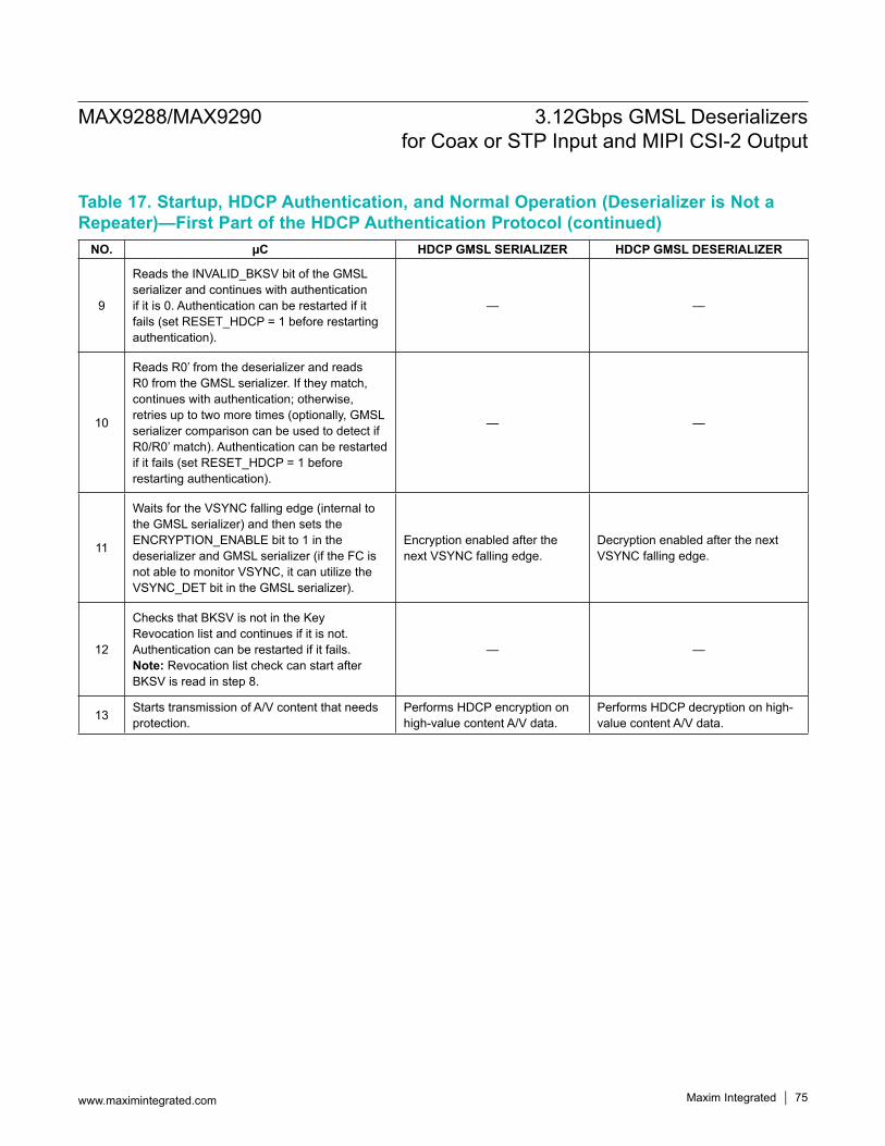
MAX9288/MAX9290 3.12Gbps GMSL Deserializers for Coax or STP Input and MIPI CSI-2 Output
www.maximintegrated.com Maxim Integrated 75
Table 17. Startup, HDCP Authentication, and Normal Operation (Deserializer is Not a Repeater)—First Part of the HDCP Authentication Protocol (continued)
NO. µC HDCP GMSL SERIALIZER HDCP GMSL DESERIALIZER
9
Reads the INVALID_BKSV bit of the GMSL serializer and continues with authentication if it is 0. Authentication can be restarted if it fails (set RESET_HDCP = 1 before restarting authentication).
— —
10
Reads R0’ from the deserializer and reads R0 from the GMSL serializer. If they match, continues with authentication; otherwise, retries up to two more times (optionally, GMSL serializer comparison can be used to detect if R0/R0’ match). Authentication can be restarted if it fails (set RESET_HDCP = 1 before restarting authentication).
— —
11
Waits for the VSYNC falling edge (internal to the GMSL serializer) and then sets the ENCRYPTION_ENABLE bit to 1 in the deserializer and GMSL serializer (if the FC is not able to monitor VSYNC, it can utilize the VSYNC_DET bit in the GMSL serializer).
Encryption enabled after the next VSYNC falling edge.
Decryption enabled after the next VSYNC falling edge.
12
Checks that BKSV is not in the Key Revocation list and continues if it is not. Authentication can be restarted if it fails.Note: Revocation list check can start after BKSV is read in step 8.
— —
13 Starts transmission of A/V content that needs protection.
Performs HDCP encryption on high-value content A/V data.
Performs HDCP decryption on high-value content A/V data.
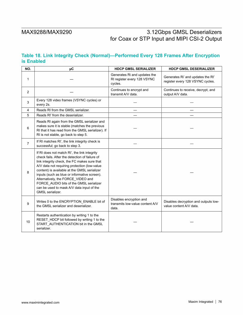
MAX9288/MAX9290 3.12Gbps GMSL Deserializers for Coax or STP Input and MIPI CSI-2 Output
www.maximintegrated.com Maxim Integrated 76
Table 18. Link Integrity Check (Normal)—Performed Every 128 Frames After Encryption is Enabled
NO. µC HDCP GMSL SERIALIZER HDCP GMSL DESERIALIZER
1 —Generates Ri and updates the RI register every 128 VSYNC cycles.
Generates Ri’ and updates the RI’ register every 128 VSYNC cycles.
2 — Continues to encrypt and transmit A/V data.
Continues to receive, decrypt, and output A/V data.
3 Every 128 video frames (VSYNC cycles) or every 2s. — —
4 Reads RI from the GMSL serializer. — —5 Reads RI’ from the deserializer. — —
6
Reads RI again from the GMSL serializer and makes sure it is stable (matches the previous RI that it has read from the GMSL serializer). If RI is not stable, go back to step 5.
— —
7 If RI matches RI’, the link integrity check is successful; go back to step 3. — —
8
If RI does not match RI’, the link integrity check fails. After the detection of failure of link integrity check, the FC makes sure that A/V data not requiring protection (low-value content) is available at the GMSL serializer inputs (such as blue or informative screen). Alternatively, the FORCE_VIDEO and FORCE_AUDIO bits of the GMSL serializer can be used to mask A/V data input of the GMSL serializer.
— —
9 Writes 0 to the ENCRYPTION_ENABLE bit of the GMSL serializer and deserializer.
Disables encryption and transmits low-value content A/V data.
Disables decryption and outputs low-value content A/V data.
10
Restarts authentication by writing 1 to the RESET_HDCP bit followed by writing 1 to the START_AUTHENTICATION bit in the GMSL serializer.
— —
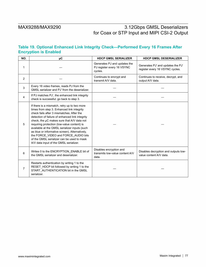
MAX9288/MAX9290 3.12Gbps GMSL Deserializers for Coax or STP Input and MIPI CSI-2 Output
www.maximintegrated.com Maxim Integrated 77
Table 19. Optional Enhanced Link Integrity Check—Performed Every 16 Frames After Encryption is Enabled
NO. µC HDCP GMSL SERIALIZER HDCP GMSL DESERIALIZER
1 —Generates PJ and updates the PJ register every 16 VSYNC cycles.
Generates PJ’ and updates the PJ’ register every 16 VSYNC cycles.
2 — Continues to encrypt and transmit A/V data.
Continues to receive, decrypt, and output A/V data.
3 Every 16 video frames, reads PJ from the GMSL serializer and PJ’ from the deserializer. — —
4 If PJ matches PJ’, the enhanced link integrity check is successful; go back to step 3. — —
5
If there is a mismatch, retry up to two more times from step 3. Enhanced link integrity check fails after 3 mismatches. After the detection of failure of enhanced link integrity check, the µC makes sure that A/V data not requiring protection (low-value content) is available at the GMSL serializer inputs (such as blue or informative screen). Alternatively, the FORCE_VIDEO and FORCE_AUDIO bits of the GMSL serializer can be used to mask A/V data input of the GMSL serializer.
— —
6 Writes 0 to the ENCRYPTION_ENABLE bit of the GMSL serializer and deserializer.
Disables encryption and transmits low-value content A/V data.
Disables decryption and outputs low-value content A/V data.
7
Restarts authentication by writing 1 to the RESET_HDCP bit followed by writing 1 to the START_AUTHENTICATION bit in the GMSL serializer.
— —
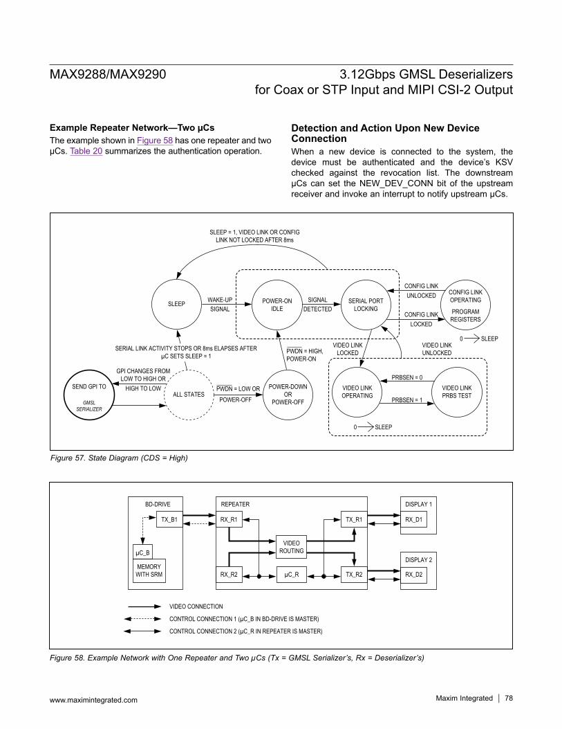
MAX9288/MAX9290 3.12Gbps GMSL Deserializers for Coax or STP Input and MIPI CSI-2 Output
www.maximintegrated.com Maxim Integrated 78
Example Repeater Network—Two µCsThe example shown in Figure 58 has one repeater and two µCs. Table 20 summarizes the authentication operation.
Detection and Action Upon New Device ConnectionWhen a new device is connected to the system, the device must be authenticated and the device’s KSV checked against the revocation list. The downstream µCs can set the NEW_DEV_CONN bit of the upstream receiver and invoke an interrupt to notify upstream µCs.
Figure 57. State Diagram (CDS = High)
Figure 58. Example Network with One Repeater and Two µCs (Tx = GMSL Serializer’s, Rx = Deserializer’s)
SLEEP
CONFIG LINKOPERATING
PROGRAMREGISTERS
POWER-OFF
HIGH TO LOW
SLEEP = 1, VIDEO LINK OR CONFIGLINK NOT LOCKED AFTER 8ms
POWER-ONIDLE
WAKE-UPSIGNAL
SERIAL PORTLOCKING
SIGNALDETECTED
CONFIG LINKUNLOCKED
CONFIG LINKLOCKED
VIDEO LINKLOCKED
VIDEO LINKUNLOCKED
0 SLEEP
0 SLEEP
ALL STATES
GPI CHANGES FROMLOW TO HIGH OR
PWDN = LOW ORSEND GPI TO
GMSLSERIALIZER
PWDN = HIGH,POWER-ON
POWER-DOWNOR
POWER-OFF
SERIAL LINK ACTIVITY STOPS OR 8ms ELAPSES AFTERµC SETS SLEEP = 1
VIDEO LINKOPERATING
PRBSEN = 0
PRBSEN = 1
VIDEO LINKPRBS TEST
BD-DRIVE
RX_R1
µC_B
TX_B1
DISPLAY 1
RX_D1
DISPLAY 2
RX_D2
REPEATER
TX_R1
TX_R2RX_R2 µC_R
VIDEOROUTING
MEMORYWITH SRM
VIDEO CONNECTION
CONTROL CONNECTION 1 (µC_B IN BD-DRIVE IS MASTER)
CONTROL CONNECTION 2 (µC_R IN REPEATER IS MASTER)
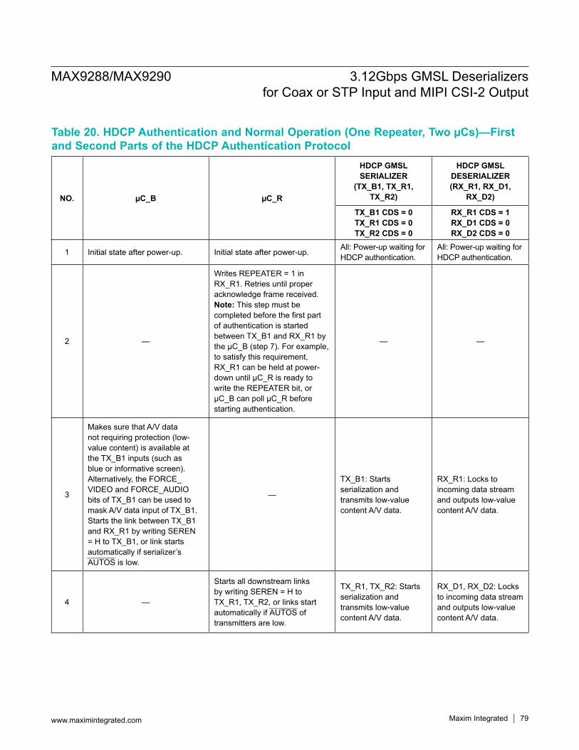
MAX9288/MAX9290 3.12Gbps GMSL Deserializers for Coax or STP Input and MIPI CSI-2 Output
www.maximintegrated.com Maxim Integrated 79
Table 20. HDCP Authentication and Normal Operation (One Repeater, Two µCs)—First and Second Parts of the HDCP Authentication Protocol
NO. µC_B µC_R
HDCP GMSL SERIALIZER
(TX_B1, TX_R1, TX_R2)
HDCP GMSL DESERIALIZER(RX_R1, RX_D1,
RX_D2)
TX_B1 CDS = 0TX_R1 CDS = 0TX_R2 CDS = 0
RX_R1 CDS = 1RX_D1 CDS = 0RX_D2 CDS = 0
1 Initial state after power-up. Initial state after power-up. All: Power-up waiting for HDCP authentication.
All: Power-up waiting for HDCP authentication.
2 —
Writes REPEATER = 1 in RX_R1. Retries until proper acknowledge frame received.Note: This step must be completed before the first part of authentication is started between TX_B1 and RX_R1 by the µC_B (step 7). For example, to satisfy this requirement, RX_R1 can be held at power-down until µC_R is ready to write the REPEATER bit, or µC_B can poll µC_R before starting authentication.
— —
3
Makes sure that A/V data not requiring protection (low-value content) is available at the TX_B1 inputs (such as blue or informative screen). Alternatively, the FORCE_VIDEO and FORCE_AUDIO bits of TX_B1 can be used to mask A/V data input of TX_B1. Starts the link between TX_B1 and RX_R1 by writing SEREN = H to TX_B1, or link starts automatically if serializer’s AUTOS is low.
—
TX_B1: Starts serialization and transmits low-value content A/V data.
RX_R1: Locks to incoming data stream and outputs low-value content A/V data.
4 —
Starts all downstream links by writing SEREN = H to TX_R1, TX_R2, or links start automatically if AUTOS of transmitters are low.
TX_R1, TX_R2: Starts serialization and transmits low-value content A/V data.
RX_D1, RX_D2: Locks to incoming data stream and outputs low-value content A/V data.
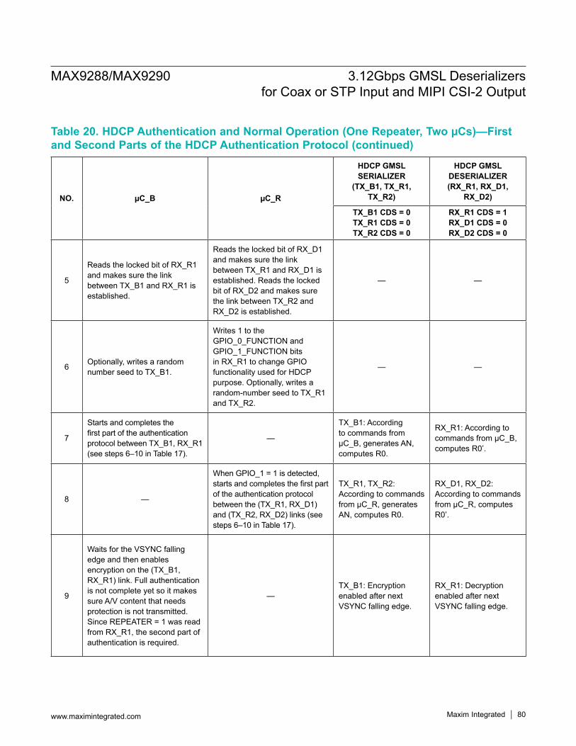
MAX9288/MAX9290 3.12Gbps GMSL Deserializers for Coax or STP Input and MIPI CSI-2 Output
www.maximintegrated.com Maxim Integrated 80
Table 20. HDCP Authentication and Normal Operation (One Repeater, Two µCs)—First and Second Parts of the HDCP Authentication Protocol (continued)
NO. µC_B µC_R
HDCP GMSL SERIALIZER
(TX_B1, TX_R1, TX_R2)
HDCP GMSL DESERIALIZER(RX_R1, RX_D1,
RX_D2)
TX_B1 CDS = 0TX_R1 CDS = 0TX_R2 CDS = 0
RX_R1 CDS = 1RX_D1 CDS = 0RX_D2 CDS = 0
5
Reads the locked bit of RX_R1 and makes sure the link between TX_B1 and RX_R1 is established.
Reads the locked bit of RX_D1 and makes sure the link between TX_R1 and RX_D1 is established. Reads the locked bit of RX_D2 and makes sure the link between TX_R2 and RX_D2 is established.
— —
6 Optionally, writes a random number seed to TX_B1.
Writes 1 to the GPIO_0_FUNCTION and GPIO_1_FUNCTION bits in RX_R1 to change GPIO functionality used for HDCP purpose. Optionally, writes a random-number seed to TX_R1 and TX_R2.
— —
7
Starts and completes the first part of the authentication protocol between TX_B1, RX_R1 (see steps 6–10 in Table 17).
—
TX_B1: According to commands from µC_B, generates AN, computes R0.
RX_R1: According to commands from µC_B, computes R0’.
8 —
When GPIO_1 = 1 is detected, starts and completes the first part of the authentication protocol between the (TX_R1, RX_D1) and (TX_R2, RX_D2) links (see steps 6–10 in Table 17).
TX_R1, TX_R2: According to commands from µC_R, generates AN, computes R0.
RX_D1, RX_D2: According to commands from µC_R, computes R0’.
9
Waits for the VSYNC falling edge and then enables encryption on the (TX_B1, RX_R1) link. Full authentication is not complete yet so it makes sure A/V content that needs protection is not transmitted. Since REPEATER = 1 was read from RX_R1, the second part of authentication is required.
—TX_B1: Encryption enabled after next VSYNC falling edge.
RX_R1: Decryption enabled after next VSYNC falling edge.
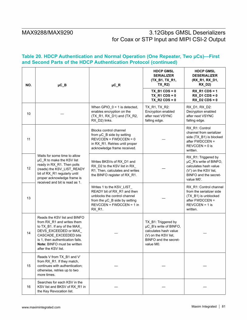
MAX9288/MAX9290 3.12Gbps GMSL Deserializers for Coax or STP Input and MIPI CSI-2 Output
www.maximintegrated.com Maxim Integrated 81
Table 20. HDCP Authentication and Normal Operation (One Repeater, Two µCs)—First and Second Parts of the HDCP Authentication Protocol (continued)
NO. µC_B µC_R
HDCP GMSL SERIALIZER
(TX_B1, TX_R1, TX_R2)
HDCP GMSL DESERIALIZER(RX_R1, RX_D1,
RX_D2)
TX_B1 CDS = 0TX_R1 CDS = 0TX_R2 CDS = 0
RX_R1 CDS = 1RX_D1 CDS = 0RX_D2 CDS = 0
10 —
When GPIO_0 = 1 is detected, enables encryption on the (TX_R1, RX_D1) and (TX_R2, RX_D2) links.
TX_R1, TX_R2: Encryption enabled after next VSYNC falling edge.
RX_D1, RX_D2: Decryption enabled after next VSYNC falling edge.
11
Waits for some time to allow µC_R to make the KSV list ready in RX_R1. Then polls (reads) the KSV_LIST_READY bit of RX_R1 regularly until proper acknowledge frame is received and bit is read as 1.
Blocks control channel from µC_B side by setting REVCCEN = FWDCCEN = 0 in RX_R1. Retries until proper acknowledge frame received.
—
RX_R1: Control channel from serializer side (TX_B1) is blocked after FWDCCEN = REVCCEN = 0 is written.
12
Writes BKSVs of RX_D1 and RX_D2 to the KSV list in RX_R1. Then, calculates and writes the BINFO register of RX_R1.
—
RX_R1: Triggered by µC_R’s write of BINFO, calculates hash value (V’) on the KSV list, BINFO and the secret-value M0’.
13
Writes 1 to the KSV_LIST_READY bit of RX_R1 and then unblocks the control channel from the µC_B side by setting REVCCEN = FWDCCEN = 1 in RX_R1.
—
RX_R1: Control channel from the serializer side (TX_B1) is unblocked after FWDCCEN = REVCCEN = 1 is written.
14
Reads the KSV list and BINFO from RX_R1 and writes them to TX_B1. If any of the MAX_DEVS_EXCEEDED or MAX_CASCADE_EXCEEDED bits is 1, then authentication fails. Note: BINFO must be written after the KSV list.
—
TX_B1: Triggered by µC_B’s write of BINFO, calculates hash value (V) on the KSV list, BINFO and the secret-value M0.
—
15
Reads V from TX_B1 and V’ from RX_R1. If they match, continues with authentication; otherwise, retries up to two more times.
— — —
16Searches for each KSV in the KSV list and BKSV of RX_R1 in the Key Revocation list.
— — —
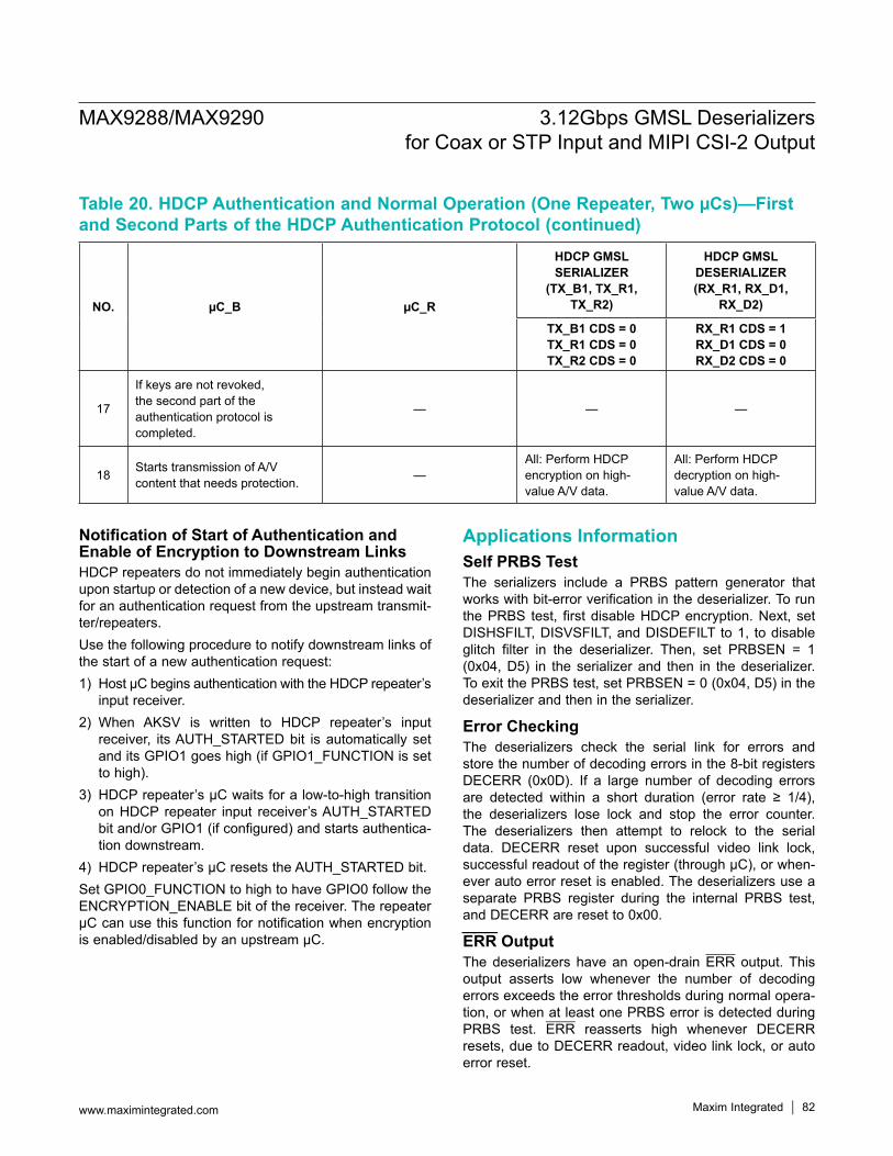
MAX9288/MAX9290 3.12Gbps GMSL Deserializers for Coax or STP Input and MIPI CSI-2 Output
www.maximintegrated.com Maxim Integrated 82
Notification of Start of Authentication and Enable of Encryption to Downstream LinksHDCP repeaters do not immediately begin authentication upon startup or detection of a new device, but instead wait for an authentication request from the upstream transmit-ter/repeaters.Use the following procedure to notify downstream links of the start of a new authentication request:1) Host µC begins authentication with the HDCP repeater’s
input receiver.2) When AKSV is written to HDCP repeater’s input
receiver, its AUTH_STARTED bit is automatically set and its GPIO1 goes high (if GPIO1_FUNCTION is set to high).
3) HDCP repeater’s µC waits for a low-to-high transition on HDCP repeater input receiver’s AUTH_STARTED bit and/or GPIO1 (if configured) and starts authentica-tion downstream.
4) HDCP repeater’s µC resets the AUTH_STARTED bit.Set GPIO0_FUNCTION to high to have GPIO0 follow the ENCRYPTION_ENABLE bit of the receiver. The repeater µC can use this function for notification when encryption is enabled/disabled by an upstream µC.
Applications InformationSelf PRBS TestThe serializers include a PRBS pattern generator that works with bit-error verification in the deserializer. To run the PRBS test, first disable HDCP encryption. Next, set DISHSFILT, DISVSFILT, and DISDEFILT to 1, to disable glitch filter in the deserializer. Then, set PRBSEN = 1 (0x04, D5) in the serializer and then in the deserializer. To exit the PRBS test, set PRBSEN = 0 (0x04, D5) in the deserializer and then in the serializer.
Error CheckingThe deserializers check the serial link for errors and store the number of decoding errors in the 8-bit registers DECERR (0x0D). If a large number of decoding errors are detected within a short duration (error rate ≥ 1/4), the deserializers lose lock and stop the error counter. The deserializers then attempt to relock to the serial data. DECERR reset upon successful video link lock, successful readout of the register (through µC), or when-ever auto error reset is enabled. The deserializers use a separate PRBS register during the internal PRBS test, and DECERR are reset to 0x00.
ERR OutputThe deserializers have an open-drain ERR output. This output asserts low whenever the number of decoding errors exceeds the error thresholds during normal opera-tion, or when at least one PRBS error is detected during PRBS test. ERR reasserts high whenever DECERR resets, due to DECERR readout, video link lock, or auto error reset.
Table 20. HDCP Authentication and Normal Operation (One Repeater, Two µCs)—First and Second Parts of the HDCP Authentication Protocol (continued)
NO. µC_B µC_R
HDCP GMSL SERIALIZER
(TX_B1, TX_R1, TX_R2)
HDCP GMSL DESERIALIZER(RX_R1, RX_D1,
RX_D2)
TX_B1 CDS = 0TX_R1 CDS = 0TX_R2 CDS = 0
RX_R1 CDS = 1RX_D1 CDS = 0RX_D2 CDS = 0
17
If keys are not revoked, the second part of the authentication protocol is completed.
— — —
18 Starts transmission of A/V content that needs protection. —
All: Perform HDCP encryption on high-value A/V data.
All: Perform HDCP decryption on high-value A/V data.
MAX9288/MAX9290 3.12Gbps GMSL Deserializers for Coax or STP Input and MIPI CSI-2 Output
www.maximintegrated.com Maxim Integrated 83
Auto Error ResetThe default method to reset errors is to read the respec-tive error registers in the deserializers (0x0D and 0x0E). Auto error reset clears the error counters DECERR and the ERR output ~1µs after ERR goes low. Auto error reset is disabled on power-up. Enable auto error reset through AUTORST (0x06, D5). Auto error reset does not run when the device is in PRBS test mode.
Dual µC ControlUsually systems have one microcontroller to run the control channel, located on the serializer side for display applications or on the deserializer side for image-sensing applications. However, a µC can reside on each side simultaneously and trade off running the control channel. In this case, each µC can communicate with the serializer and deserializer and any peripheral devices.Contention occurs if both µCs attempt to use the control channel at the same time. It is up to the user to prevent this contention by implementing a higher level protocol. In addition, the control channel does not provide arbitration between I2C masters on both sides of the link. An acknowledge frame is not generated when communication fails due to contention. If communication across the serial link is not required, the µCs can disable the forward and reverse control channel using the FWDCCEN and REVCCEN bits (0x04, D[1:0]) in the serializer/deserializer. Communication across the serial link is stopped and contention between µCs cannot occur.As an example of dual µC use in an image-sensing appli-cation, the serializer can be in sleep mode and waiting for wake-up by µC on the deserializer side. After wake-up, the serializer-side µC assumes master control of the serializer’s registers.
Changing the Clock FrequencyIt is recommended that the serial link be enabled after the video clock (fpixel) and the control-channel clock (fUART/fI2C) are stable. When changing the clock frequency, stop the video clock for 5µs, apply the clock at the new frequency, then restart the serial link or toggle SEREN. On-the-fly changes in clock frequency are possible if the new frequency is immediately stable and without glitches. The reverse control channel remains unavailable for 500µs after serial link start or stop. When using the UART interface, limit on-the-fly changes in fUART to factors of less than 3.5 at a time to ensure that the device recognizes the UART sync pattern. For example, when lowering the UART frequency from 1Mbps to 100kbps, first send data at 333kbps then at 100kbps for reduction ratios of 3 and 3.333, respectively.
Spread-Spectrum Clock TrackingUsing a spread-spectrum clock source can reduce EMI/EMC on the serial and MIPI data. The deserializer can track a spread-spectrum signal from the serializer. Use a spread < ±1% for CSI-2 output rates ≤ 400MHz. Use a spread < ±0.5% for CSI-2 output rates > 400MHz.
Fast Detection of Loss-of-SynchronizationA measure of link quality is the recovery time from loss- of-synchronization. The host can be quickly notified of loss-of-lock by connecting the deserializer’s LOCK out-put to the GPI input. If other sources use the GPI input, such as a touch-screen controller, the µC can implement a routine to distinguish between interrupts from loss-of-sync and normal interrupts. Reverse control-channel communication does not require an active forward link to operate and accurately tracks the LOCK status of the GMSL link. LOCK asserts for video link only and not for the configuration link.
Providing a Frame Sync (Camera Applications)The GPI/GPO provide a simple solution for camera applications that require a frame sync signal from the ECU (e.g., surround-view systems). Connect the ECU frame sync signal to the GPI input, and connect GPO output to the camera frame sync input. GPI/GPO has a typical delay of 275µs. Skew between multiple GPI/GPO channels is typically 115µs. If a lower skew signal is required, connect the camera’s frame sync input to one of the deserializer’s GPIOs and use an I2C broadcast write command to change the GPIO output state. This has a maximum skew of 1.5µs, independent from the used I2C bit rate.
Software Programming of the Device AddressesThe serializers and deserializers have programmable device addresses. This allows multiple GMSL devices, along with I2C peripherals, to coexist on the same control channel. The serializer device address is in register 0x00 of each device, while the deserializer device address is in register 0x01 of each device. To change a device address, first write to the device whose address changes (register 0x00 of the serializer for serializer device address change, or register 0x01 of the deserializer for deserializer device address change). Then write the same address into the corresponding register on the other device (register 0x00 of the deserializer for serializer device address change, or register 0x01 of the serializer for deserializer device address change).
MAX9288/MAX9290 3.12Gbps GMSL Deserializers for Coax or STP Input and MIPI CSI-2 Output
www.maximintegrated.com Maxim Integrated 84
Three-Level Configuration InputsCX/TP and BWS are three-level inputs that control the seri-al interface configuration and power-up defaults. Connect three-level inputs through a pullup resistor to IOVDD to set a high level, a pulldown resistor to GND to set a low level, or open to set a mid level. For digital control, use three-state logic to drive the three-level logic input.
Configuration BlockingThe deserializers can block changes to registers. Set CFGBLOCK to make registers 0x00 to 0x1F as read only. Once set, the registers remain blocked until the supplies are removed or until PWDN is low.
Compatibility with Other GMSL DevicesThe deserializers are designed to pair with the MAX9275–MAX9281 serializers, but interoperate with any GMSL serializers. See Table 21 for operating limitations
Key MemoryEach device has a unique HDCP key set that is stored in secure nonvolatile memory (NVM). The HDCP key set consists of 40 56-bit private keys and one 40-bit public key. The NVM is qualified for automotive applications.
HS/VS/DE InversionThe deserializers use an active-high HS, VS, and DE for encoding and HDCP encryption. Set INVHSYNC, INVVSYNC, and INVDE in the serializer to invert active-low input signals for use with the GMSL devices. Set INVHSYNC, INVVSYNC, and INVDE in the deserializer (register 0x14) to output active-low signals for use with downstream devices.
WS/SCK InversionThe deserializers use standard polarities for I2S. Set INVWS and INVSCK in the serializer (register 0x1B) to invert opposite polarity signals for use with the GMSL devices. Set INVWS and INVSCK in the deserializer (register 0x1D) to output reverse-polarity signals for downstream use.
GPIOsThe deserializers have two open-drain GPIOs available when not used for HDCP purposes (see the Notification of Start of Authentication and Enable of Encryption to Downstream Links section), GPIO1OUT and GPIO0OUT (0x06, D3 and D1) set the output state of the GPIOs. Setting the GPIO output bits to 0 low pulls the output low, while setting the bits to 1 leaves the output undriven, and pulled high through internal/external pullup resistors. The GPIO input buffers are always enabled. The input states are stored in GPIO1 and GPIO0 (0x06, D2 and D0). Set GPIO1OUT/GPIO0OUT to 1 when using GPIO1/GPIO0 as an input.
Line-Fault DetectionThe line-fault detector monitors for line failures such as short to ground, short to battery, and open link for system-fault diagnosis. Figure 1 shows the required external resistor connections. LFLT = low when a line fault is detected and LFLT goes high when the line returns to normal. The line-fault type is stored in 0x08 D[3:0] of the serializer. Filter LFLT with the µC to reduce the detector’s susceptibility to short ground shifts. The fault-detector threshold voltages are referenced to the serializer ground. Additional passive components set the DC level of the cable. If the serializer and GMSL deserializer grounds are different, the link DC voltage during normal operation can vary and cross one of the fault-detection thresholds.
Table 21. MAX9288/MAX9290 Feature CompatibilityFEATURE GMSL SERIALIZER
HDCP (MAX9290 only) If feature not supported in serializer, must not be turned on in the MAX9290.High-bandwidth mode If feature not supported in serializer, must only use 24-bit and 32-bit modes.I2C-to-I2C If feature not supported in serializer, must use UART-to-I2C or UART-to-UART.
Coax If feature not supported in serializer, must connect unused serial output through 200nF and 50Ω in series to VDD and set the reverse control channel amplitude to 100mV.
High-immunity control channel If feature not supported in serializer, must use the legacy reverse control-channel mode.
TDM encoding If feature not supported in serializer, must use I2S encoding (with 50% WS duty cycle), if supported.
I2S encoding If feature not supported in serializer, must disable I2S in the MAX9288/MAX9290.
MAX9288/MAX9290 3.12Gbps GMSL Deserializers for Coax or STP Input and MIPI CSI-2 Output
www.maximintegrated.com Maxim Integrated 85
For the fault-detection circuit, select the resistor’s power rating to handle a short to the battery. In coax mode, leave the unused line-fault inputs unconnected. To detect the short-together case, refer to Application Note 4709: GMSL Line-Fault Detection. Table 23 lists the mapping for line fault types
Internal Input PulldownsThe control and configuration inputs (except three-level inputs) include a pulldown resistor to GND. External pulldown resistors are not needed.
Choosing I2C/UART Pullup ResistorsI2C and UART open-drain lines require a pullup resistor to provide a logic-high level. There are tradeoffs between power dissipation and speed, and a compromise may be required when choosing pullup resistor values. Every device connected to the bus introduces some capacitance even when the device is not in operation. I2C specifies 300ns rise times (30% to 70%) for fast mode, which is defined for data rates up to 400kbps (see the I2C specifications in the AC Electrical Characteristics table for details). To meet the fast-mode rise-time requirement, choose the pullup resistors so that rise time tR = 0.85 x RPULLUP x CBUS < 300ns. The waveforms are not recognized if the transition time becomes too slow. The device supports I2C/UART rates up to 1Mbps.
AC-CouplingAC-coupling isolates the receiver from DC voltages up to the voltage rating of the capacitor. Capacitors at the serializer output and at the deserializer input are needed for proper link operation and to provide protection if either end of the cable is shorted to a battery. AC-coupling blocks low-frequency ground shifts and low-frequency common-mode noise.
Selection of AC-Coupling CapacitorsVoltage droop and the digital sum variation (DSV) of transmitted symbols cause signal transitions to start from different voltage levels. Because the transition time is fixed, starting the signal transition from different voltage levels causes timing jitter. The time constant for an AC-coupled link needs to be chosen to reduce droop and jitter to an acceptable level. The RC network for an AC-coupled link consists of the CML/coax receiver termination resistor (RTR), the CML/coax driver termination resistor (RTD), and the series AC-coupling capacitors (C). The RC time constant for four equal-value series capacitors is (C x (RTD + RTR))/4. RTD and RTR are required to match the transmission line impedance (usually 100Ω
differential, 50Ω single ended). This leaves the capacitor selection to change the system time constant. Use at 0.22μF (using legacy reverse control channel), 47nF (using high-immunity reverse control channel), or larger high-frequency surface-mount ceramic capacitors, with sufficient voltage rating to withstand a short to battery, to pass the lower speed reverse control-channel signal. Use capacitors with a case size less than 3.2mm x 1.6mm to have lower parasitic effects to the high-speed signal.
Power-Supply Circuits and BypassingThe deserializers use an AVDD18 and DVDD18 of 1.7V to 1.9V and an AVDD3 of 3.0V to 3.6V. All single-ended inputs and outputs except for the serial input derive power from an IOVDD of 1.7V to 3.6V that scale with IOVDD. Proper voltage-supply bypassing is essential for high-frequency circuit stability.
Power-Supply TablePower-supply currents shown in the DC Electrical Characteristics table is measured at VIOVDD = 3.6V. If using a different IOVDD voltage, the IOVDD worst-case supply current will vary. HDCP operation (MAX9290 only) draws additional current. This is shown in Table 24.
Cables and ConnectorsInterconnect for CML typically has a differential impedance of 100Ω. Use cables and connectors that have matched differential impedance to minimize imped-ance discontinuities. Coax cables typically have a characteristic impedance of 50Ω, contact the factory for 75Ω operation). Table 24 lists the suggested cables and connectors used in the GMSL link.
Board LayoutSeparate LVCMOS logic signals and CML/coax high-speed signals to prevent crosstalk. Use a four-layer PCB with separate layers for power, ground, CML/coax, and LVCMOS logic signals. Layout PCB traces close to each other for a 100Ω differential characteristic impedance for STP. The trace dimensions depend on the type of trace used (microstrip or stripline). Note that two 50Ω PCB traces do not have 100Ω differential impedance when brought close together—the impedance goes down when the traces are brought closer. Use a 50Ω trace for the single-ended output when driving coax.Route the PCB traces for differential CML channel in parallel to maintain the differential characteristic imped-ance. Avoid vias. Keep PCB traces that make up a differential pair equal length to avoid skew within the differential pair.
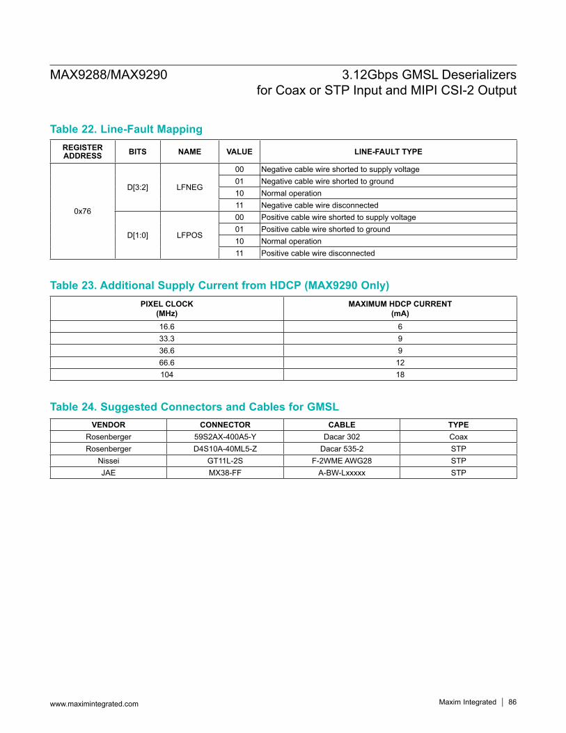
MAX9288/MAX9290 3.12Gbps GMSL Deserializers for Coax or STP Input and MIPI CSI-2 Output
www.maximintegrated.com Maxim Integrated 86
Table 22. Line-Fault Mapping
Table 23. Additional Supply Current from HDCP (MAX9290 Only)
Table 24. Suggested Connectors and Cables for GMSL
REGISTER ADDRESS BITS NAME VALUE LINE-FAULT TYPE
0x76
D[3:2] LFNEG
00 Negative cable wire shorted to supply voltage01 Negative cable wire shorted to ground10 Normal operation11 Negative cable wire disconnected
D[1:0] LFPOS
00 Positive cable wire shorted to supply voltage01 Positive cable wire shorted to ground10 Normal operation11 Positive cable wire disconnected
PIXEL CLOCK(MHz)
MAXIMUM HDCP CURRENT(mA)
16.6 633.3 936.6 966.6 12104 18
VENDOR CONNECTOR CABLE TYPERosenberger 59S2AX-400A5-Y Dacar 302 CoaxRosenberger D4S10A-40ML5-Z Dacar 535-2 STP
Nissei GT11L-2S F-2WME AWG28 STPJAE MX38-FF A-BW-Lxxxxx STP
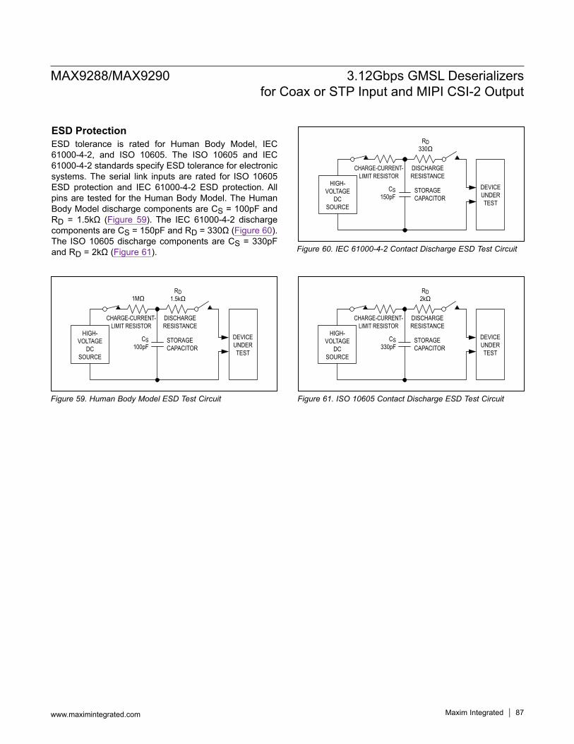
MAX9288/MAX9290 3.12Gbps GMSL Deserializers for Coax or STP Input and MIPI CSI-2 Output
www.maximintegrated.com Maxim Integrated 87
ESD ProtectionESD tolerance is rated for Human Body Model, IEC 61000-4-2, and ISO 10605. The ISO 10605 and IEC 61000-4-2 standards specify ESD tolerance for electronic systems. The serial link inputs are rated for ISO 10605 ESD protection and IEC 61000-4-2 ESD protection. All pins are tested for the Human Body Model. The Human Body Model discharge components are CS = 100pF and RD = 1.5kΩ (Figure 59). The IEC 61000-4-2 discharge components are CS = 150pF and RD = 330Ω (Figure 60). The ISO 10605 discharge components are CS = 330pF and RD = 2kΩ (Figure 61).
Figure 59. Human Body Model ESD Test Circuit
Figure 60. IEC 61000-4-2 Contact Discharge ESD Test Circuit
Figure 61. ISO 10605 Contact Discharge ESD Test Circuit
CS150pF
STORAGECAPACITOR
HIGH-VOLTAGE
DCSOURCE
DEVICEUNDERTEST
CHARGE-CURRENT-LIMIT RESISTOR
DISCHARGERESISTANCE
RD330Ω
STORAGECAPACITOR
HIGH-VOLTAGE
DCSOURCE
DEVICEUNDERTEST
CHARGE-CURRENT-LIMIT RESISTOR
DISCHARGERESISTANCE
1MΩRD
1.5kΩ
CS100pF
STORAGECAPACITOR
HIGH-VOLTAGE
DCSOURCE
DEVICEUNDERTEST
CHARGE-CURRENT-LIMIT RESISTOR
DISCHARGERESISTANCE
RD2kΩ
CS330pF
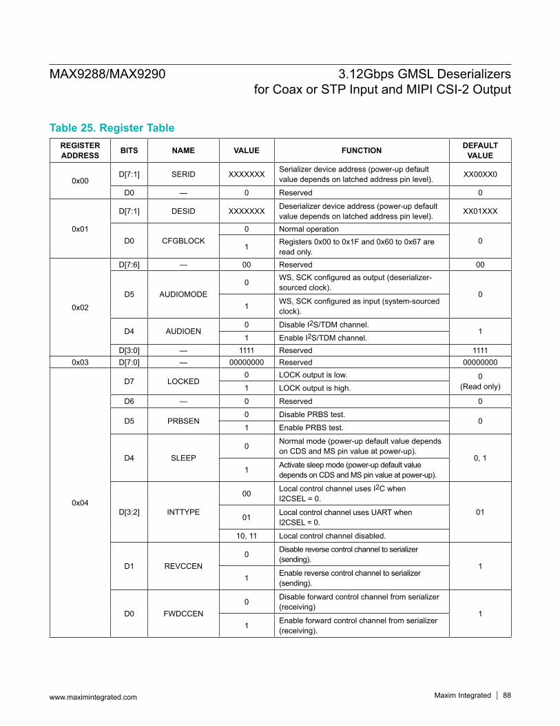
MAX9288/MAX9290 3.12Gbps GMSL Deserializers for Coax or STP Input and MIPI CSI-2 Output
www.maximintegrated.com Maxim Integrated 88
Table 25. Register TableREGISTER ADDRESS BITS NAME VALUE FUNCTION DEFAULT
VALUE
0x00D[7:1] SERID XXXXXXX Serializer device address (power-up default
value depends on latched address pin level). XX00XX0
D0 — 0 Reserved 0
0x01
D[7:1] DESID XXXXXXX Deserializer device address (power-up default value depends on latched address pin level). XX01XXX
D0 CFGBLOCK0 Normal operation
01 Registers 0x00 to 0x1F and 0x60 to 0x67 are
read only.
0x02
D[7:6] — 00 Reserved 00
D5 AUDIOMODE0 WS, SCK configured as output (deserializer-
sourced clock).0
1 WS, SCK configured as input (system-sourced clock).
D4 AUDIOEN0 Disable I2S/TDM channel.
11 Enable I2S/TDM channel.
D[3:0] — 1111 Reserved 11110x03 D[7:0] — 00000000 Reserved 00000000
0x04
D7 LOCKED0 LOCK output is low. 0
(Read only)1 LOCK output is high.D6 — 0 Reserved 0
D5 PRBSEN0 Disable PRBS test.
01 Enable PRBS test.
D4 SLEEP0 Normal mode (power-up default value depends
on CDS and MS pin value at power-up).0, 1
1 Activate sleep mode (power-up default value depends on CDS and MS pin value at power-up).
D[3:2] INTTYPE
00 Local control channel uses I2C when I2CSEL = 0.
0101 Local control channel uses UART when I2CSEL = 0.
10, 11 Local control channel disabled.
D1 REVCCEN0 Disable reverse control channel to serializer
(sending).1
1 Enable reverse control channel to serializer (sending).
D0 FWDCCEN0 Disable forward control channel from serializer
(receiving)1
1 Enable forward control channel from serializer (receiving).
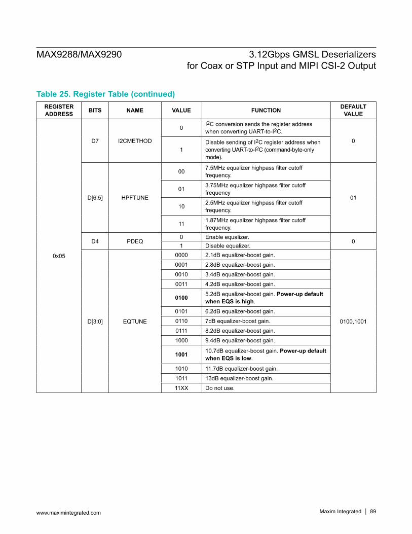
MAX9288/MAX9290 3.12Gbps GMSL Deserializers for Coax or STP Input and MIPI CSI-2 Output
www.maximintegrated.com Maxim Integrated 89
Table 25. Register Table (continued)REGISTER ADDRESS BITS NAME VALUE FUNCTION DEFAULT
VALUE
0x05
D7 I2CMETHOD
0 I2C conversion sends the register address when converting UART-to-I2C.
01
Disable sending of I2C register address when converting UART-to-I2C (command-byte-only mode).
D[6:5] HPFTUNE
00 7.5MHz equalizer highpass filter cutoff frequency.
0101 3.75MHz equalizer highpass filter cutoff
frequency
10 2.5MHz equalizer highpass filter cutoff frequency.
11 1.87MHz equalizer highpass filter cutoff frequency.
D4 PDEQ0 Enable equalizer.
01 Disable equalizer.
D[3:0] EQTUNE
0000 2.1dB equalizer-boost gain.
0100,1001
0001 2.8dB equalizer-boost gain.0010 3.4dB equalizer-boost gain.0011 4.2dB equalizer-boost gain.
0100 5.2dB equalizer-boost gain. Power-up default when EQS is high.
0101 6.2dB equalizer-boost gain.0110 7dB equalizer-boost gain.0111 8.2dB equalizer-boost gain.1000 9.4dB equalizer-boost gain.
1001 10.7dB equalizer-boost gain. Power-up default when EQS is low.
1010 11.7dB equalizer-boost gain.1011 13dB equalizer-boost gain.11XX Do not use.
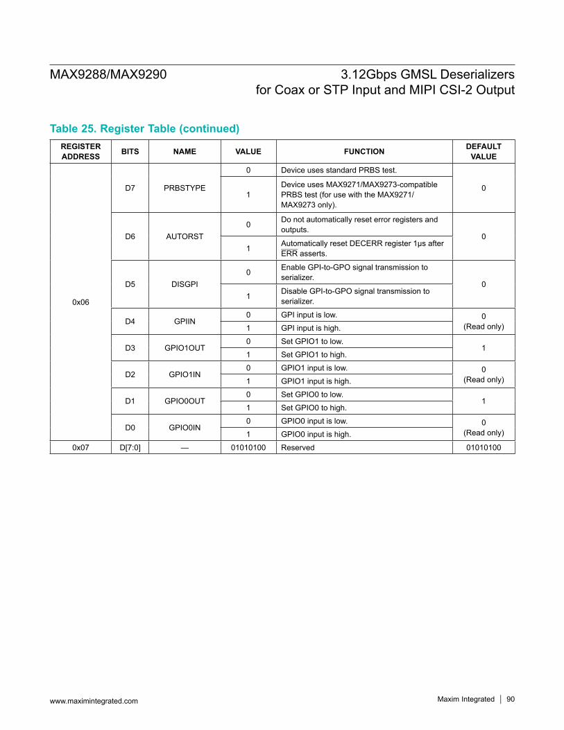
MAX9288/MAX9290 3.12Gbps GMSL Deserializers for Coax or STP Input and MIPI CSI-2 Output
www.maximintegrated.com Maxim Integrated 90
Table 25. Register Table (continued)REGISTER ADDRESS BITS NAME VALUE FUNCTION DEFAULT
VALUE
0x06
D7 PRBSTYPE
0 Device uses standard PRBS test.
01
Device uses MAX9271/MAX9273-compatible PRBS test (for use with the MAX9271/ MAX9273 only).
D6 AUTORST0 Do not automatically reset error registers and
outputs.0
1 Automatically reset DECERR register 1µs after ERR asserts.
D5 DISGPI0 Enable GPI-to-GPO signal transmission to
serializer.0
1 Disable GPI-to-GPO signal transmission to serializer.
D4 GPIIN0 GPI input is low. 0
(Read only)1 GPI input is high.
D3 GPIO1OUT0 Set GPIO1 to low.
11 Set GPIO1 to high.
D2 GPIO1IN0 GPIO1 input is low. 0
(Read only)1 GPIO1 input is high.
D1 GPIO0OUT0 Set GPIO0 to low.
11 Set GPIO0 to high.
D0 GPIO0IN0 GPIO0 input is low. 0
(Read only)1 GPIO0 input is high.0x07 D[7:0] — 01010100 Reserved 01010100
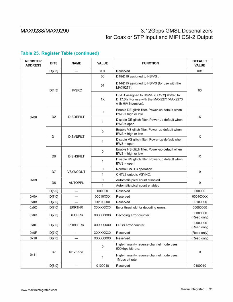
MAX9288/MAX9290 3.12Gbps GMSL Deserializers for Coax or STP Input and MIPI CSI-2 Output
www.maximintegrated.com Maxim Integrated 91
Table 25. Register Table (continued)REGISTER ADDRESS BITS NAME VALUE FUNCTION DEFAULT
VALUE
0x08
D[7:5] — 001 Reserved 001
D[4:3] HVSRC
00 D18/D19 assigned to HS/VS .
0001 D14/D15 assigned to HS/VS (for use with the
MAX9271).
1XD0/D1 assigned to HS/VS (D[19:2] shifted to D[17:0]). For use with the MAX9271/MAX9273 with H/V inversion).
D2 DISDEFILT0 Enable DE glitch filter. Power-up default when
BWS = high or low.X
1 Disable DE glitch filter. Power-up default when BWS = open.
D1 DISVSFILT0 Enable VS glitch filter. Power-up default when
BWS = high or low.X
1 Disable VS glitch filter. Power-up default when BWS = open.
D0 DISHSFILT0 Enable HS glitch filter. Power-up default when
BWS = high or low.X
1 Disable HS glitch filter. Power-up default when BWS = open.
0x09
D7 VSYNCOUT0 Normal CNTL3 operation.
01 CNTL3 outputs VSYNC.
D6 AUTOPPL0 Automatic pixel count disabled.
01 Automatic pixel count enabled.
D[5:0] — 000000 Reserved 0000000x0A D[7:0] — 00010XXX Reserved 00010XXX0x0B D[7:0] — 00100000 Reserved 001000000x0C D[7:0] ERRTHR XXXXXXXX Error threshold for decoding errors. 00000000
0x0D D[7:0] DECERR XXXXXXXX Decoding error counter. 00000000(Read only)
0x0E D[7:0] PRBSERR XXXXXXXX PRBS error counter. 00000000(Read only)
0x0F D[7:0] — XXXXXXXX Reserved (Read only)0x10 D[7:0] — XXXXXXXX Reserved (Read only)
0x11D7 REVFAST
0 High-immunity reverse channel mode uses 500kbps bit rate.
01 High-immunity reverse channel mode uses
1Mbps bit rate.
D[6:0] — 0100010 Reserved 0100010
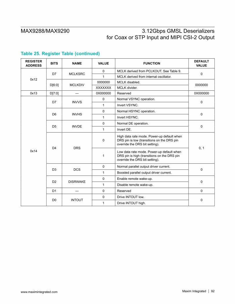
MAX9288/MAX9290 3.12Gbps GMSL Deserializers for Coax or STP Input and MIPI CSI-2 Output
www.maximintegrated.com Maxim Integrated 92
Table 25. Register Table (continued)REGISTER ADDRESS BITS NAME VALUE FUNCTION DEFAULT
VALUE
0x12D7 MCLKSRC
0 MCLK derived from PCLKOUT. See Table 9.0
1 MCLK derived from internal oscillator.
D[6:0] MCLKDIV0000000 MCLK disabled.
0000000XXXXXXX MCLK divider.
0x13 D[7:0] — 0X000000 Reserved 0X000000
0x14
D7 INVVS0 Normal VSYNC operation.
01 Invert VSYNC.
D6 INVHS0 Normal HSYNC operation.
01 Invert HSYNC.
D5 INVDE0 Normal DE operation.
01 Invert DE.
D4 DRS
0High data rate mode. Power-up default when DRS pin is low (transitions on the DRS pin override the DRS bit setting).
0, 1
1Low data rate mode. Power-up default when DRS pin is high (transitions on the DRS pin override the DRS bit setting).
D3 DCS0 Normal parallel output driver current.
01 Boosted parallel output driver current.
D2 DISRWAKE0 Enable remote wake-up.
01 Disable remote wake-up.
D1 — 0 Reserved 0
D0 INTOUT0 Drive INTOUT low.
01 Drive INTOUT high.
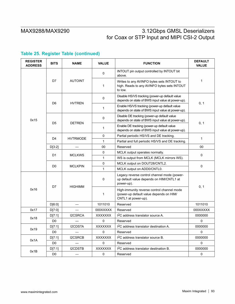
MAX9288/MAX9290 3.12Gbps GMSL Deserializers for Coax or STP Input and MIPI CSI-2 Output
www.maximintegrated.com Maxim Integrated 93
Table 25. Register Table (continued)REGISTER ADDRESS BITS NAME VALUE FUNCTION DEFAULT
VALUE
0x15
D7 AUTOINT
0 INTOUT pin output controlled by INTOUT bit above.
11
Writes to any AVINFO bytes sets INTOUT to high. Reads to any AVINFO bytes sets INTOUT to low.
D6 HVTREN0 Disable HS/VS tracking (power-up default value
depends on state of BWS input value at power-up).0, 1
1 Enable HS/VS tracking (power-up default value depends on state of BWS input value at power-up).
D5 DETREN0 Disable DE tracking (power-up default value
depends on state of BWS input value at power-up).0, 1
1 Enable DE tracking (power-up default value depends on state of BWS input value at power-up).
D4 HVTRMODE0 Partial periodic HS/VS and DE tracking.
11 Partial and full periodic HS/VS and DE tracking.
D[3:2] — 00 Reserved 00
D1 MCLKWS0 MCLK output operates normally.
01 WS is output from MCLK (MCLK mirrors WS).
D0 MCLKPIN0 MCLK output on DOUT28/CNTL2.
01 MCLK output on ADD0/CNTL0.
0x16D7 HIGHIMM
0Legacy reverse control channel mode (power-up default value depends on HIM/CNTL1 at power-up).
0, 1
1High-immunity reverse control channel mode (power-up default value depends on HIM/CNTL1 at power-up).
D[6:0] — 1011010 Reserved 10110100x17 D[7:0] — 000XXXXX Reserved 000XXXXX
0x18D[7:1] I2CSRCA XXXXXXX I2C address translator source A. 0000000
D0 — 0 Reserved 0
0x19D[7:1] I2CDSTA XXXXXXX I2C address translator destination A. 0000000
D0 — 0 Reserved 0
0x1AD[7:1] I2CSRCB XXXXXXX I2C address translator source B. 0000000
D0 — 0 Reserved 0
0x1BD[7:1] I2CDSTB XXXXXXX I2C address translator destination B. 0000000
D0 — 0 Reserved 0
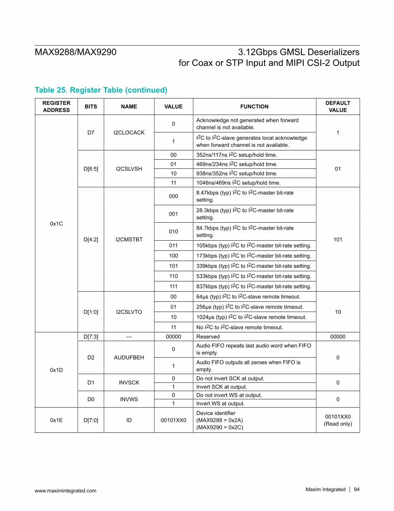
MAX9288/MAX9290 3.12Gbps GMSL Deserializers for Coax or STP Input and MIPI CSI-2 Output
www.maximintegrated.com Maxim Integrated 94
Table 25. Register Table (continued)REGISTER ADDRESS BITS NAME VALUE FUNCTION DEFAULT
VALUE
0x1C
D7 I2CLOCACK0 Acknowledge not generated when forward
channel is not available.1
1 I2C to I2C-slave generates local acknowledge when forward channel is not available.
D[6:5] I2CSLVSH
00 352ns/117ns I2C setup/hold time.
0101 469ns/234ns I2C setup/hold time.10 938ns/352ns I2C setup/hold time.11 1046ns/469ns I2C setup/hold time.
D[4:2] I2CMSTBT
000 8.47kbps (typ) I2C to I2C-master bit-rate setting.
101
001 28.3kbps (typ) I2C to I2C-master bit-rate setting.
010 84.7kbps (typ) I2C to I2C-master bit-rate setting.
011 105kbps (typ) I2C to I2C-master bit-rate setting.
100 173kbps (typ) I2C to I2C-master bit-rate setting.
101 339kbps (typ) I2C to I2C-master bit-rate setting.
110 533kbps (typ) I2C to I2C-master bit-rate setting.
111 837kbps (typ) I2C to I2C-master bit-rate setting.
D[1:0] I2CSLVTO
00 64µs (typ) I2C to I2C-slave remote timeout.
1001 256µs (typ) I2C to I2C-slave remote timeout.
10 1024µs (typ) I2C to I2C-slave remote timeout.
11 No I2C to I2C-slave remote timeout.
0x1D
D[7:3] — 00000 Reserved 00000
D2 AUDUFBEH0 Audio FIFO repeats last audio word when FIFO
is empty.0
1 Audio FIFO outputs all zeroes when FIFO is empty.
D1 INVSCK0 Do not invert SCK at output.
01 Invert SCK at output.
D0 INVWS0 Do not invert WS at output.
01 Invert WS at output.
0x1E D[7:0] ID 00101XX0Device identifier(MAX9288 = 0x2A)(MAX9290 = 0x2C)
00101XX0(Read only)
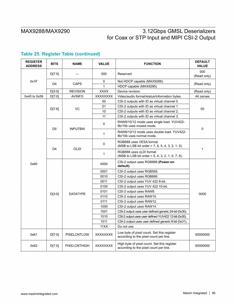
MAX9288/MAX9290 3.12Gbps GMSL Deserializers for Coax or STP Input and MIPI CSI-2 Output
www.maximintegrated.com Maxim Integrated 95
Table 25. Register Table (continued)REGISTER ADDRESS BITS NAME VALUE FUNCTION DEFAULT
VALUE
0x1F
D[7:5] — 000 Reserved 000(Read only)
D4 CAPS0 Not HDCP capable (MAX9288).
(Read only)1 HDCP capable (MAX9290).
D[3:0] REVISION XXXX Device revision. (Read only)0x40 to 0x59 D[7:0] AVINFO XXXXXXXX Video/audio format/status/information bytes. All zeroes
0x60
D[7:6] VC
00 CSI-2 outputs with ID as virtual channel 0.
0001 CSI-2 outputs with ID as virtual channel 1.10 CSI-2 outputs with ID as virtual channel 2.11 CSI-2 outputs with ID as virtual channel 3.
D5 INPUTBW0 RAW8/10/12 mode uses single load. YUV422-
8b/10b uses muxed mode.0
1 RAW8/10/12 mode uses double load. YUV422-8b/10b uses normal mode.
D4 OLDI0 RGB888 uses VESA format
(MSB to LSB bit order = 7, 6, 5, 4, 3, 2, 1, 0).1
1 RGB888 uses oLDI format (MSB to LSB bit order = 5, 4, 3, 2, 1, 0, 7, 6).
D[3:0] DATATYPE
0000 CSI-2 output uses RGB888 (Power-on default).
0000
0001 CSI-2 output uses RGB565.0010 CSI-2 output uses RGB666.0011 CSI-2 output uses YUV 422 8-bit.0100 CSI-2 output uses YUV 422 10-bit.0101 CSI-2 output uses RAW8.0110 CSI-2 output uses RAW10.0111 CSI-2 output uses RAW12.1000 CSI-2 output uses RAW14.1001 CSI-2 output uses user defined generic 24-bit (0x30).1010 CSI-2 output uses user defined YUV422 12-bit (0x30).1011 CSI-2 output uses user defined generic 8-bit (0x31).11XX Do not use.
0x61 D[7:0] PIXELCNTLOW XXXXXXXX Low byte of pixel count. Set this register according to the pixel count per line. 00000000
0x62 D[7:0] PIXELCNTHIGH XXXXXXXX High byte of pixel count. Set this register according to the pixel count per line. 00000000
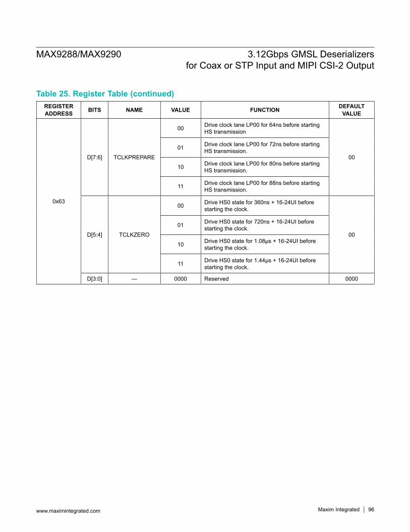
MAX9288/MAX9290 3.12Gbps GMSL Deserializers for Coax or STP Input and MIPI CSI-2 Output
www.maximintegrated.com Maxim Integrated 96
Table 25. Register Table (continued)REGISTER ADDRESS BITS NAME VALUE FUNCTION DEFAULT
VALUE
0x63
D[7:6] TCLKPREPARE
00 Drive clock lane LP00 for 64ns before starting HS transmission
0001 Drive clock lane LP00 for 72ns before starting
HS transmission.
10 Drive clock lane LP00 for 80ns before starting HS transmission.
11 Drive clock lane LP00 for 88ns before starting HS transmission.
D[5:4] TCLKZERO
00 Drive HS0 state for 360ns + 16-24UI before starting the clock.
0001 Drive HS0 state for 720ns + 16-24UI before
starting the clock.
10 Drive HS0 state for 1.08µs + 16-24UI before starting the clock.
11 Drive HS0 state for 1.44µs + 16-24UI before starting the clock.
D[3:0] — 0000 Reserved 0000
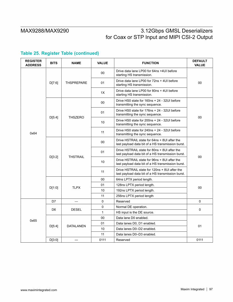
MAX9288/MAX9290 3.12Gbps GMSL Deserializers for Coax or STP Input and MIPI CSI-2 Output
www.maximintegrated.com Maxim Integrated 97
Table 25. Register Table (continued)REGISTER ADDRESS BITS NAME VALUE FUNCTION DEFAULT
VALUE
0x64
D[7:6] THSPREPARE
00 Drive data lane LP00 for 64ns +4UI before starting HS transmission.
0001 Drive data lane LP00 for 72ns + 4UI before starting HS transmission.
1X Drive data lane LP00 for 80ns + 4UI before starting HS transmission.
D[5:4] THSZERO
00 Drive HS0 state for 160ns + 24 - 32UI before transmitting the sync sequence.
0001 Drive HS0 state for 176ns + 24 - 32UI before
transmitting the sync sequence.
10 Drive HS0 state for 200ns + 24 - 32UI before transmitting the sync sequence.
11 Drive HS0 state for 240ns + 24 - 32UI before transmitting the sync sequence.
D[3:2] THSTRAIL
00 Drive HSTRAIL state for 64ns + 8UI after the last payload data bit of a HS transmission burst.
0001 Drive HSTRAIL state for 80ns + 8UI after the
last payload data bit of a HS transmission burst.
10 Drive HSTRAIL state for 96ns + 8UI after the last payload data bit of a HS transmission burst.
11 Drive HSTRAIL state for 120ns + 8UI after the last payload data bit of a HS transmission burst.
D[1:0] TLPX
00 64ns LPTX period length.
0001 128ns LPTX period length.10 192ns LPTX period length.11 256ns LPTX period length
0x65
D7 — 0 Reserved 0
D6 DESEL0 Normal DE operation.
01 HS input is the DE source.
D[5:4] DATALANEN
00 Data lane D0 enabled.
0101 Data lanes D0, D1 enabled.10 Data lanes D0–D2 enabled.11 Data lanes D0–D3 enabled.
D[3:0] — 0111 Reserved 0111
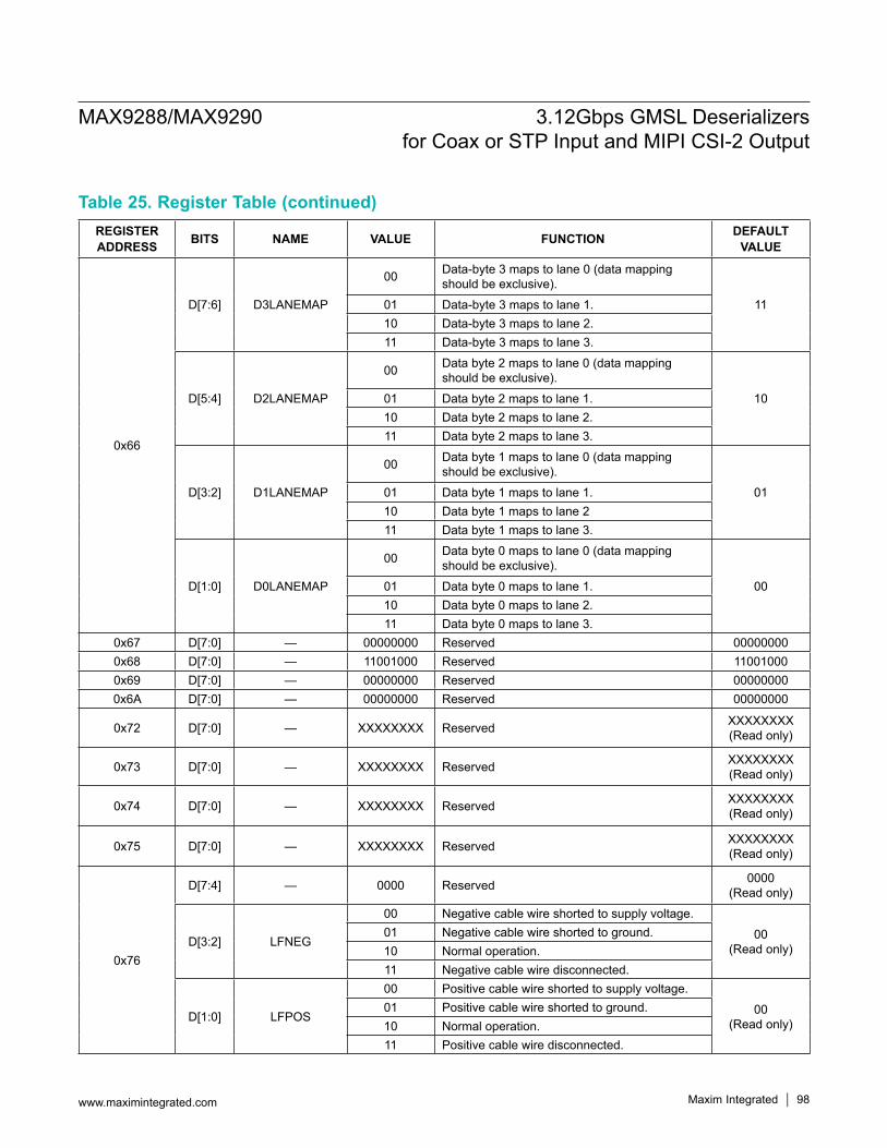
MAX9288/MAX9290 3.12Gbps GMSL Deserializers for Coax or STP Input and MIPI CSI-2 Output
www.maximintegrated.com Maxim Integrated 98
Table 25. Register Table (continued)REGISTER ADDRESS BITS NAME VALUE FUNCTION DEFAULT
VALUE
0x66
D[7:6] D3LANEMAP
00 Data-byte 3 maps to lane 0 (data mapping should be exclusive).
1101 Data-byte 3 maps to lane 1.10 Data-byte 3 maps to lane 2.11 Data-byte 3 maps to lane 3.
D[5:4] D2LANEMAP
00 Data byte 2 maps to lane 0 (data mapping should be exclusive).
1001 Data byte 2 maps to lane 1.10 Data byte 2 maps to lane 2.11 Data byte 2 maps to lane 3.
D[3:2] D1LANEMAP
00 Data byte 1 maps to lane 0 (data mapping should be exclusive).
0101 Data byte 1 maps to lane 1.10 Data byte 1 maps to lane 211 Data byte 1 maps to lane 3.
D[1:0] D0LANEMAP
00 Data byte 0 maps to lane 0 (data mapping should be exclusive).
0001 Data byte 0 maps to lane 1.10 Data byte 0 maps to lane 2.11 Data byte 0 maps to lane 3.
0x67 D[7:0] — 00000000 Reserved 000000000x68 D[7:0] — 11001000 Reserved 110010000x69 D[7:0] — 00000000 Reserved 000000000x6A D[7:0] — 00000000 Reserved 00000000
0x72 D[7:0] — XXXXXXXX Reserved XXXXXXXX (Read only)
0x73 D[7:0] — XXXXXXXX Reserved XXXXXXXX (Read only)
0x74 D[7:0] — XXXXXXXX Reserved XXXXXXXX (Read only)
0x75 D[7:0] — XXXXXXXX Reserved XXXXXXXX (Read only)
0x76
D[7:4] — 0000 Reserved 0000 (Read only)
D[3:2] LFNEG
00 Negative cable wire shorted to supply voltage.00
(Read only)01 Negative cable wire shorted to ground.10 Normal operation.11 Negative cable wire disconnected.
D[1:0] LFPOS
00 Positive cable wire shorted to supply voltage.00
(Read only)01 Positive cable wire shorted to ground.10 Normal operation.11 Positive cable wire disconnected.
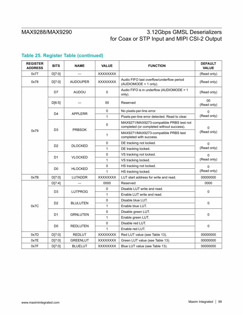
MAX9288/MAX9290 3.12Gbps GMSL Deserializers for Coax or STP Input and MIPI CSI-2 Output
www.maximintegrated.com Maxim Integrated 99
Table 25. Register Table (continued)REGISTER ADDRESS BITS NAME VALUE FUNCTION DEFAULT
VALUE0x77 D[7:0] — XXXXXXXX (Read only)
0x78 D[7:0] AUDOUPER XXXXXXXX Audio FIFO last overflow/underflow period (AUDIOMODE = 1 only). (Read only)
0x79
D7 AUDOU 0 Audio FIFO is in underflow (AUDIOMODE = 1 only). (Read only)
D[6:5] — 00 Reserved 00 (Read only)
D4 APPLERR0 No pixels-per-line error. 0
(Read only)1 Pixels-per-line error detected. Read to clear.
D3 PRBSOK0 MAX9271/MAX9273-compatible PRBS test not
completed (or completed without success). 0 (Read only)
1 MAX9271/MAX9273-compatible PRBS test completed with success.
D2 DLOCKED0 DE tracking not locked. 0
(Read only)1 DE tracking locked.
D1 VLOCKED0 VS tracking not locked. 0
(Read only)1 VS tracking locked.
D0 HLOCKED0 HS tracking not locked. 0
(Read only)1 HS tracking locked.0x7B D[7:0] LUTADDR XXXXXXXX LUT start address for write and read. 00000000
0x7C
D[7:4] — 0000 Reserved 0000
D3 LUTPROG0 Disable LUT write and read.
01 Enable LUT write and read.
D2 BLULUTEN0 Disable blue LUT.
01 Enable blue LUT.
D1 GRNLUTEN0 Disable green LUT.
01 Enable green LUT.
D0 REDLUTEN0 Disable red LUT.
01 Enable red LUT.
0x7D D[7:0] REDLUT XXXXXXXX Red LUT value (see Table 13). 000000000x7E D[7:0] GREENLUT XXXXXXXX Green LUT value (see Table 13). 000000000x7F D[7:0] BLUELUT XXXXXXXX Blue LUT value (see Table 13). 00000000
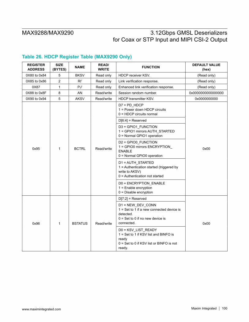
MAX9288/MAX9290 3.12Gbps GMSL Deserializers for Coax or STP Input and MIPI CSI-2 Output
www.maximintegrated.com Maxim Integrated 100
Table 26. HDCP Register Table (MAX9290 Only)REGISTER ADDRESS
SIZE(BYTES) NAME READ/
WRITE FUNCTION DEFAULT VALUE(hex)
0X80 to 0x84 5 BKSV Read only HDCP receiver KSV. (Read only)0X85 to 0x86 2 RI’ Read only Link verification response. (Read only)
0X87 1 PJ’ Read only Enhanced link verification response. (Read only)0X88 to 0x8F 8 AN Read/write Session random number. 0x00000000000000000X90 to 0x94 5 AKSV Read/write HDCP transmitter KSV. 0x0000000000
0x95 1 BCTRL Read/write
D7 = PD_HDCP1 = Power down HDCP circuits0 = HDCP circuits normal
0x00
D[6:4] = Reserved
D3 = GPIO1_FUNCTION1 = GPIO1 mirrors AUTH_STARTED0 = Normal GPIO1 operation
D2 = GPIO0_FUNCTION1 = GPIO0 mirrors ENCRYPTION_ENABLE0 = Normal GPIO0 operation
D1 = AUTH_STARTED1 = Authentication started (triggered by write to AKSV)0 = Authentication not started
D0 = ENCRYPTION_ENABLE1 = Enable encryption0 = Disable encryption
0x96 1 BSTATUS Read/write
D[7:2] = Reserved
0x00
D1 = NEW_DEV_CONN1 = Set to 1 if a new connected device is detected.0 = Set to 0 if no new device is connected.
D0 = KSV_LIST_READY1 = Set to 1 if KSV list and BINFO is ready0 = Set to 0 if KSV list or BINFO is not ready.
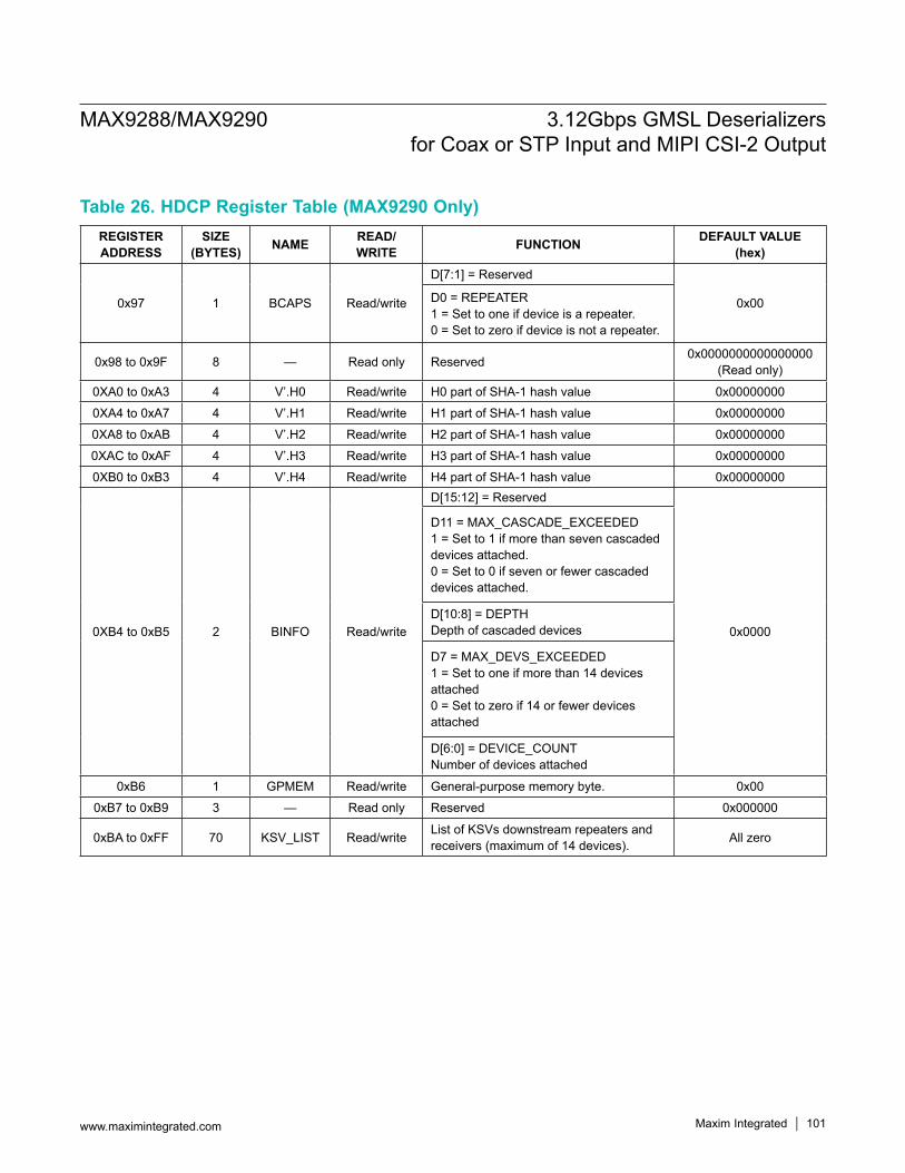
MAX9288/MAX9290 3.12Gbps GMSL Deserializers for Coax or STP Input and MIPI CSI-2 Output
www.maximintegrated.com Maxim Integrated 101
Table 26. HDCP Register Table (MAX9290 Only)REGISTER ADDRESS
SIZE(BYTES) NAME READ/
WRITE FUNCTION DEFAULT VALUE(hex)
0x97 1 BCAPS Read/write
D[7:1] = Reserved
0x00D0 = REPEATER1 = Set to one if device is a repeater.0 = Set to zero if device is not a repeater.
0x98 to 0x9F 8 — Read only Reserved 0x0000000000000000(Read only)
0XA0 to 0xA3 4 V’.H0 Read/write H0 part of SHA-1 hash value 0x000000000XA4 to 0xA7 4 V’.H1 Read/write H1 part of SHA-1 hash value 0x000000000XA8 to 0xAB 4 V’.H2 Read/write H2 part of SHA-1 hash value 0x000000000XAC to 0xAF 4 V’.H3 Read/write H3 part of SHA-1 hash value 0x000000000XB0 to 0xB3 4 V’.H4 Read/write H4 part of SHA-1 hash value 0x00000000
0XB4 to 0xB5 2 BINFO Read/write
D[15:12] = Reserved
0x0000
D11 = MAX_CASCADE_EXCEEDED1 = Set to 1 if more than seven cascaded devices attached.0 = Set to 0 if seven or fewer cascaded devices attached.
D[10:8] = DEPTHDepth of cascaded devices
D7 = MAX_DEVS_EXCEEDED1 = Set to one if more than 14 devices attached0 = Set to zero if 14 or fewer devices attached
D[6:0] = DEVICE_COUNTNumber of devices attached
0xB6 1 GPMEM Read/write General-purpose memory byte. 0x000xB7 to 0xB9 3 — Read only Reserved 0x000000
0xBA to 0xFF 70 KSV_LIST Read/write List of KSVs downstream repeaters and receivers (maximum of 14 devices). All zero
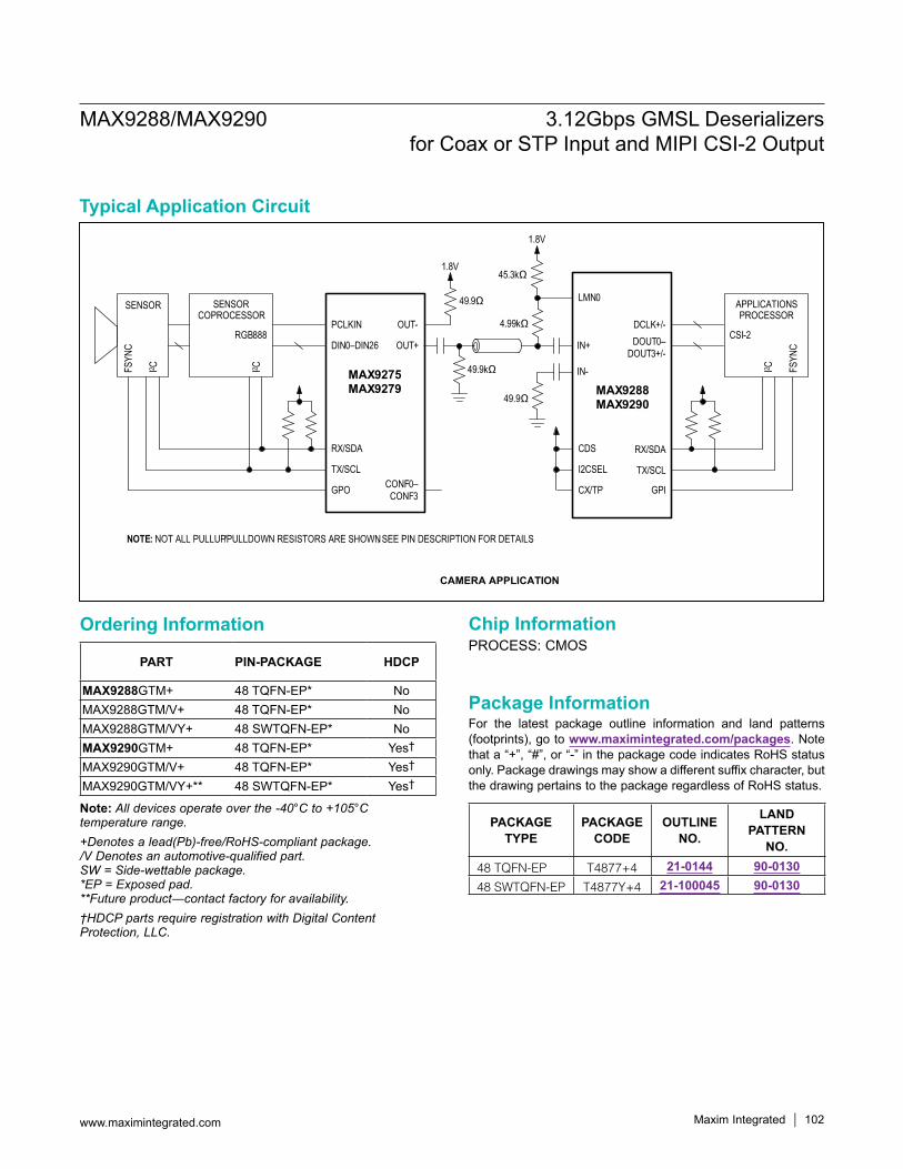
MAX9288/MAX9290 3.12Gbps GMSL Deserializers for Coax or STP Input and MIPI CSI-2 Output
www.maximintegrated.com Maxim Integrated 102
Note: All devices operate over the -40°C to +105°C temperature range.+Denotes a lead(Pb)-free/RoHS-compliant package. /V Denotes an automotive-qualified part. SW = Side-wettable package. *EP = Exposed pad. **Future product―contact factory for availability.†HDCP parts require registration with Digital Content Protection, LLC.
PART PIN-PACKAGE HDCP
MAX9288GTM+ 48 TQFN-EP* NoMAX9288GTM/V+ 48 TQFN-EP* NoMAX9288GTM/VY+ 48 SWTQFN-EP* NoMAX9290GTM+ 48 TQFN-EP* Yes†
MAX9290GTM/V+ 48 TQFN-EP* Yes†
MAX9290GTM/VY+** 48 SWTQFN-EP* Yes†
PACKAGE TYPE
PACKAGE CODE
OUTLINE NO.
LAND PATTERN
NO.48 TQFN-EP T4877+4 21-0144 90-013048 SWTQFN-EP T4877Y+4 21-100045 90-0130
NOTE: NOT ALL PULLUP/PULLDOWN RESISTORS ARE SHOWN. SEE PIN DESCRIPTION FOR DETAILS.
CAMERA APPLICATION
SENSOR
DIN0–DIN26
PCLKIN
RX/SDA
TX/SCL
GPO
OUT+
OUT-
49.9Ω
1.8V
CONF0–CONF3
RGB888
FSYN
C
I2 C
SENSORCOPROCESSOR
I2 C MAX9275MAX9279
49.9kΩ
1.8V
IN+
IN-
LMN0
DCLK+/-DOUT0–
DOUT3+/-
RX/SDA
TX/SCL
GPI
I2CSEL
CX/TP
CDS
45.3kΩ
4.99kΩ
49.9ΩMAX9288MAX9290
FSYN
C
I2 C
APPLICATIONSPROCESSOR
CSI-2
Typical Application Circuit
Ordering Information
Package InformationFor the latest package outline information and land patterns (footprints), go to www.maximintegrated.com/packages. Note that a “+”, “#”, or “-” in the package code indicates RoHS status only. Package drawings may show a different suffix character, but the drawing pertains to the package regardless of RoHS status.
Chip InformationPROCESS: CMOS
Maxim Integrated cannot assume responsibility for use of any circuitry other than circuitry entirely embodied in a Maxim Integrated product. No circuit patent licenses are implied. Maxim Integrated reserves the right to change the circuitry and specifications without notice at any time. The parametric values (min and max limits) shown in the Electrical Characteristics table are guaranteed. Other parametric values quoted in this data sheet are provided for guidance.
Maxim Integrated and the Maxim Integrated logo are trademarks of Maxim Integrated Products, Inc.
MAX9288/MAX9290 3.12Gbps GMSL Deserializers for Coax or STP Input and MIPI CSI-2 Output
© 2018 Maxim Integrated Products, Inc. 103
REVISIONNUMBER
REVISIONDATE DESCRIPTION PAGES
CHANGED0 3/14 Initial release —
1 9/14 Added simplified diagram, removed Table 1 and renumbered the subsequent tables, clarified functions, removed future product designations, and corrected typos
1, 28, 33, 48, 49, 51–56, 59, 66, 67, 69–72, 74–77, 79–82,
84, 85, 86, 88–102
2 11/15 Clarified timing requirements 8, 27, 30, 50
3 3/17 Various updates, beginning with AC Electrical Characteristics
12, 18, 21, 26, 58, 61, 62, 67, 71, 80, 84, 86,
90, 99
4 3/18Deleted QFND package and added side-wettable TQFN (SWTQFN) to General Description, Absolute Maximum Ratings, Package Thermal Characteristics, Pin Configuration, Ordering Information, and Package Information
1, 8, 18, 102
Revision History
For pricing, delivery, and ordering information, please contact Maxim Direct at 1-888-629-4642, or visit Maxim Integrated’s website at www.maximintegrated.com.