MAS836 – Sensor Technologies for Interactive Environments · Images of incorrect and correct...
36
MAS836 – Sensor Technologies for Interactive Environments Lecture 3 – Analog Conditioning Electronics, Pt. 3 Original images © source unknown. All rights reserved. This content is excluded from our Creative Commons license. For more information, see http://ocw.mit.edu/fairuse.
Transcript of MAS836 – Sensor Technologies for Interactive Environments · Images of incorrect and correct...
MAS836 – Sensor Technologies for Interactive Environments
Lecture 3 – Analog Conditioning Electronics, Pt. 3
Original images © source unknown. All rights reserved. This content is excluded from our Creative Commons license. For more information, see http://ocw.mit.edu/fairuse.
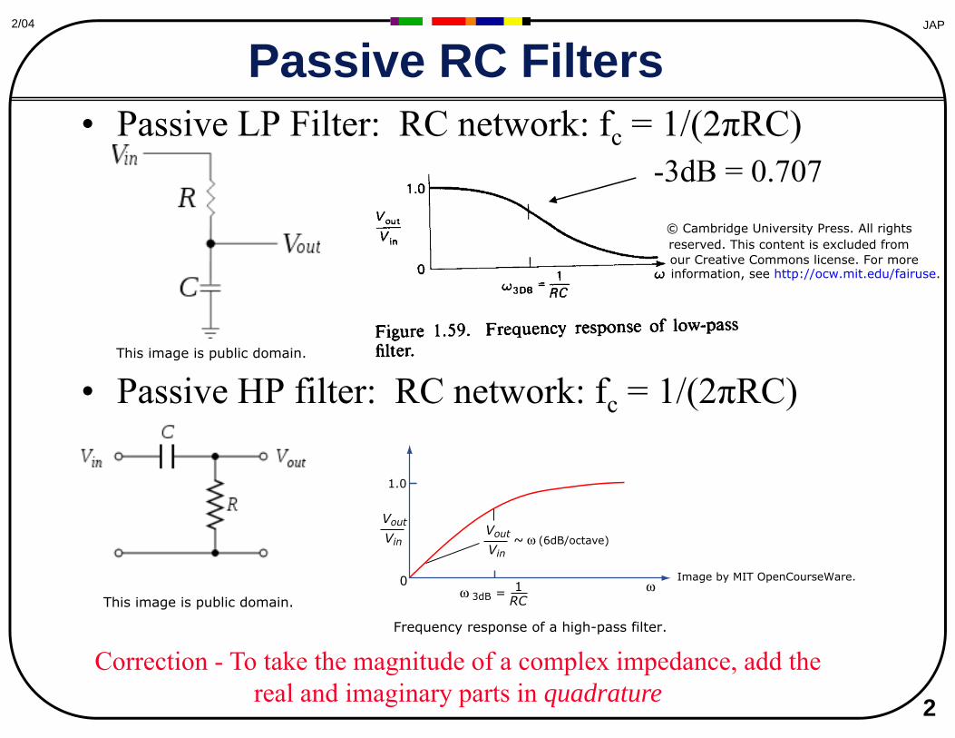
• Passive LP Filter: RC network: f = 1/(2πRC)
JAP2/04
Passive RC Filters c
• Passive HP filter: RC network: fc = 1/(2πRC)
-3dB = 0.707
Correction - To take the magnitude of a complex impedance, add the real and imaginary parts in quadrature 2
This image is public domain.
This image is public domain.
© Cambridge University Press. All rights reserved. This content is excluded from our Creative Commons license. For more information, see http://ocw.mit.edu/fairuse.
1.0
ω 3dB = 1RC
Vout
Vin
0 ω
Vout
Vin~ ω (6dB/octave)
Frequency response of a high-pass filter.
Image by MIT OpenCourseWare.
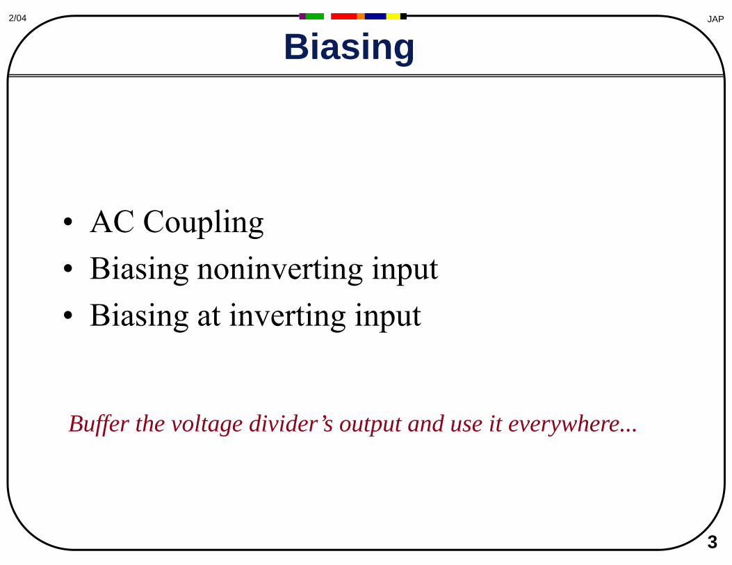
3
JAP2/04
Biasing
• AC Coupling • Biasing noninverting input • Biasing at inverting input
Buffer the voltage divider’s output and use it everywhere...
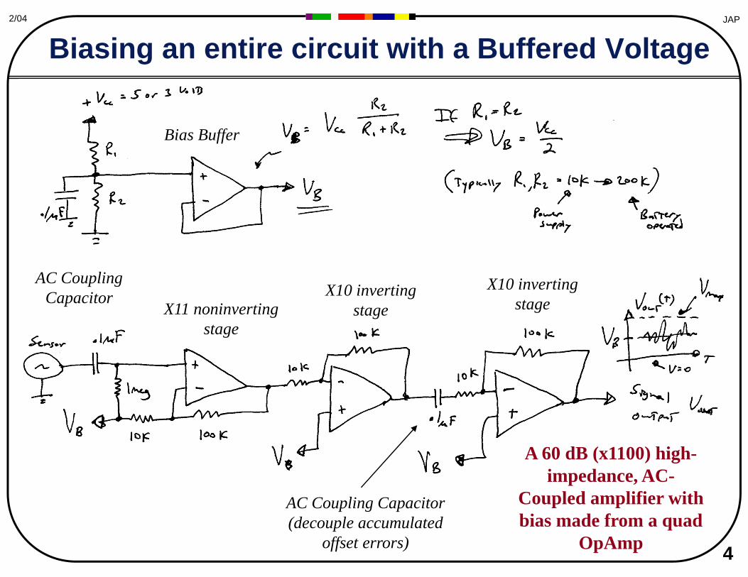
2/04 JAP
Biasing an entire circuit with a Buffered Voltage
Bias Buffer
AC Coupling Capacitor
X11 noninverting stage
X10 invertingstage
AC Coupling Capacitor (decouple accumulated
offset errors)
X10 inverting stage
A 60 dB (x1100) high-impedance, AC-
Coupled amplifier with bias made from a quad
OpAmp 4
5
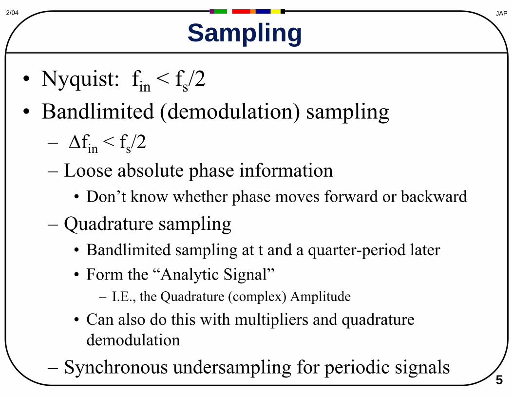
JAP2/04
Sampling
• Nyquist: fin < fs/2 • Bandlimited (demodulation) sampling
– Δfin < fs/2 – Loose absolute phase information
• Don’t know whether phase moves forward or backward
– Quadrature sampling • Bandlimited sampling at t and a quarter-period later • Form the “Analytic Signal”
– I.E., the Quadrature (complex) Amplitude
• Can also do this with multipliers and quadrature demodulation
– Synchronous undersampling for periodic signals
6
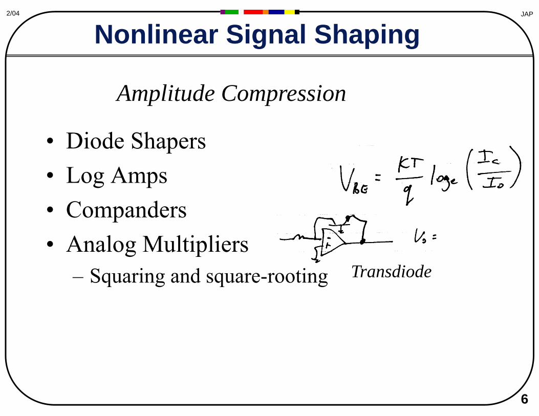
JAP2/04
Nonlinear Signal Shaping
• Diode Shapers • Log Amps • Companders • Analog Multipliers
– Squaring and square-rooting Transdiode
Amplitude Compression
7
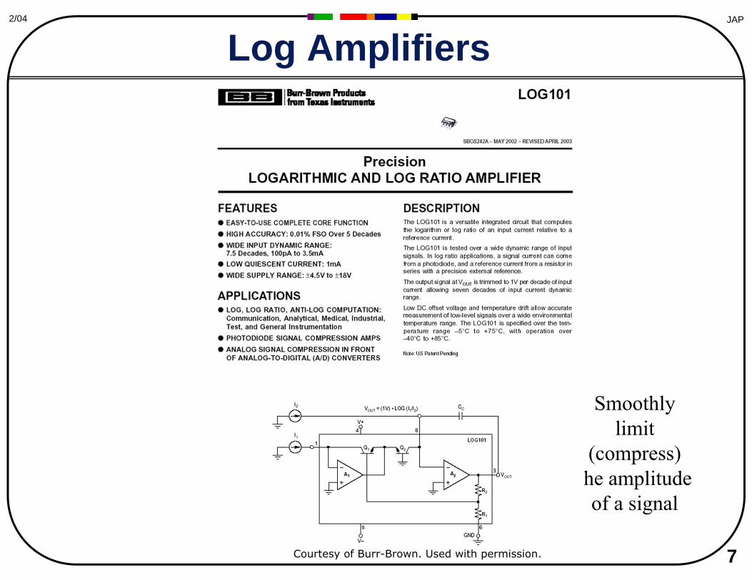
JAP2/04
Log Amplifiers
Smoothly limit
(compress) the amplitude
of a signal
Courtesy of Burr-Brown. Used with permission.
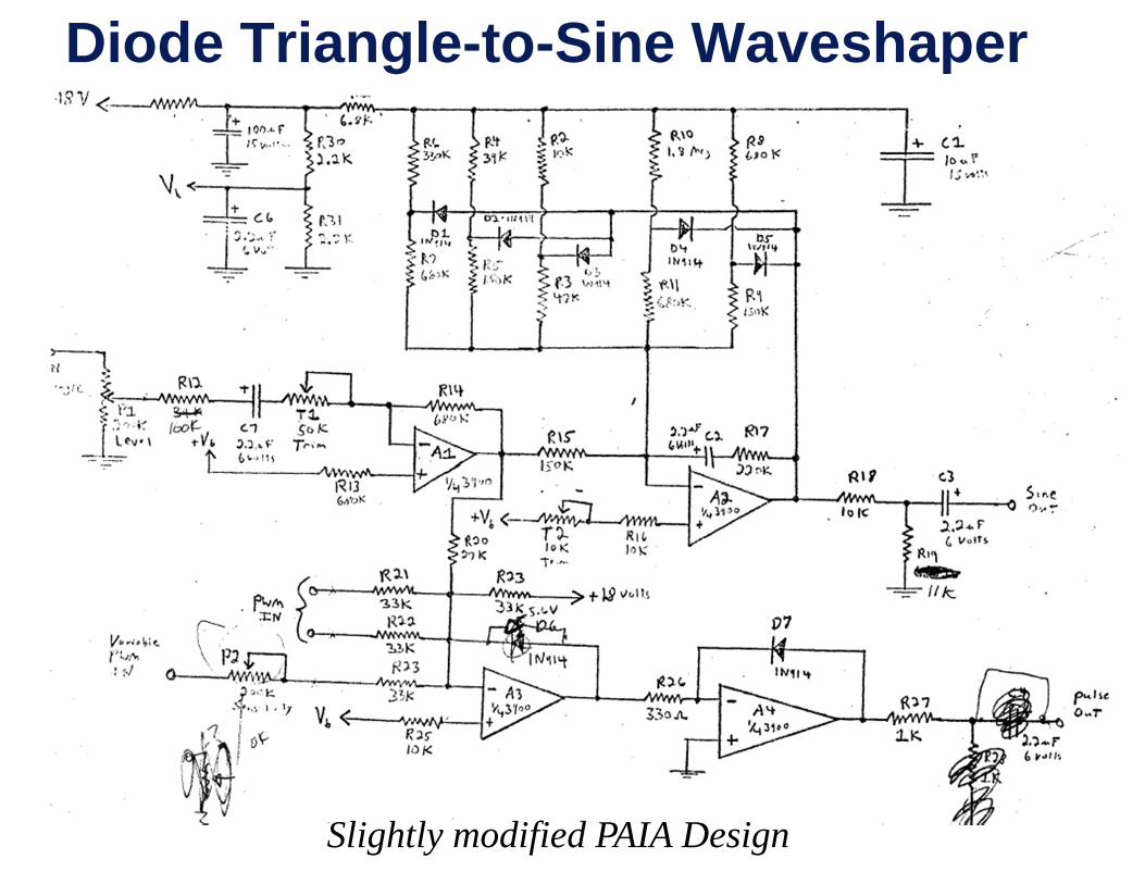
Diode Triangle-to-Sine Waveshaper
Slightly modified PAIA Design
11
JAP2/04
Digitization
• Can use an analog-digital converter (ADC) – 8-12 bit converters commonly on µComputers
• Sometimes 16 or 24 bit (µConverter from Analog) – For special applications, one can use an ADC chip
• Typically talk SPI, I2C, etc. – Many kinds of ADC
• Pipeline, Successive Approximation, Flash, ΣΔ… • Ari will tell you lots about how these work and their characteristics
• For just 1 or 2 bits, you can use comparators – Comparitors often on µC chip too
• You can also convert an amplitude into a time signal – Only need a logic pin and a timing routine (or internal µC timer) – Voltage to pulse-width, voltage to frequency
• Can do current too!
12
JAP2/04
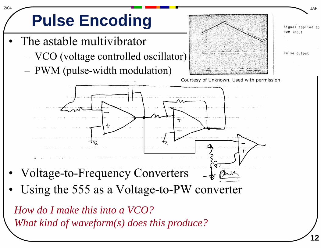
Pulse Encoding • The astable multivibrator
– VCO (voltage controlled oscillator)– PWM (pulse-width modulation)
• Voltage-to-Frequency Converters • Using the 555 as a Voltage-to-PW converter
How do I make this into a VCO? What kind of waveform(s) does this produce?
Courtesy of Unknown. Used with permission.
14
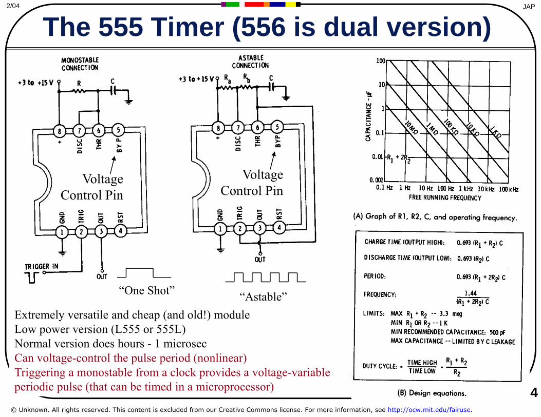
2/04 JAP
The 555 Timer (556 is dual version)
“One Shot” “Astable” Extremely versatile and cheap (and old!) module Low power version (L555 or 555L) Normal version does hours - 1 microsec Can voltage-control the pulse period (nonlinear) Triggering a monostable from a clock provides a voltage-variable periodic pulse (that can be timed in a microprocessor)
Voltage Control Pin
Voltage Control Pin
© Unknown. All rights reserved. This content is excluded from our Creative Commons license. For more information, see http://ocw.mit.edu/fairuse.
JAP2/04
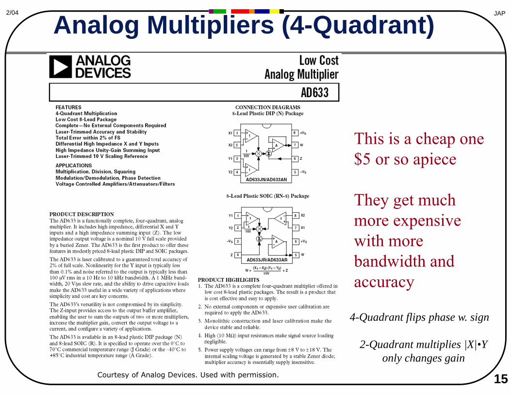
Analog Multipliers (4-Quadrant)
This is a cheap one $5 or so apiece
They get much more expensive with more bandwidth and accuracy
-Quadrant flips phase w. sign
2-Quadrant multiplies |X|•Y only changes gain
15
4
Courtesy of Analog Devices. Used with permission.
6
JAP2/04
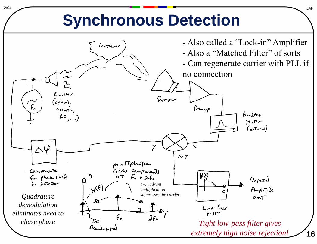
Synchronous Detection
f
4-Quadrant multiplication suppresses the carrier
- Also called a “Lock-in” Amplifier - Also a “Matched Filter” of sorts - Can regenerate carrier with PLL if no connection
Tight low-pass filter gives extremely high noise rejection! 1
Quadrature demodulation
eliminates need to chase phase
2/04 JAP
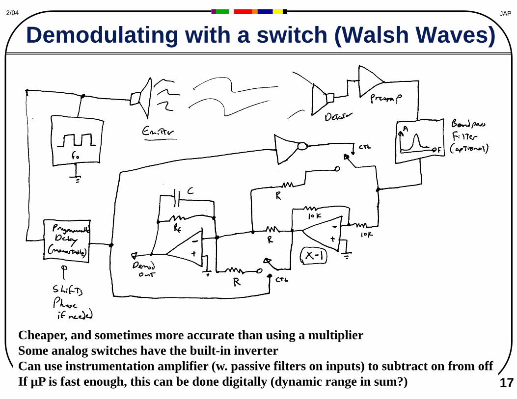
Demodulating with a switch (Walsh Waves)
Cheaper, and sometimes more accurate than using a multiplier Some analog switches have the built-in inverter Can use instrumentation amplifier (w. passive filters on inputs) to subtract on from off If µP is fast enough, this can be done digitally (dynamic range in sum?) 17
18
JAP2/04
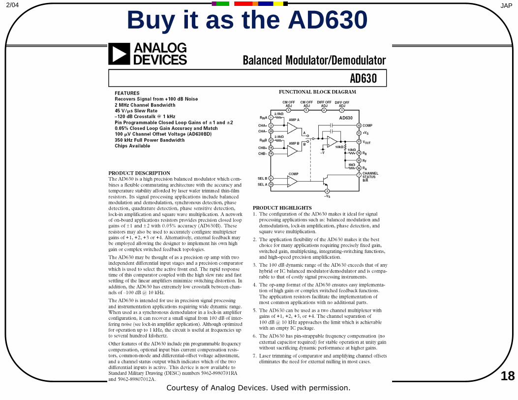
Buy it as the AD630
Courtesy of Analog Devices. Used with permission.
JAP2/04
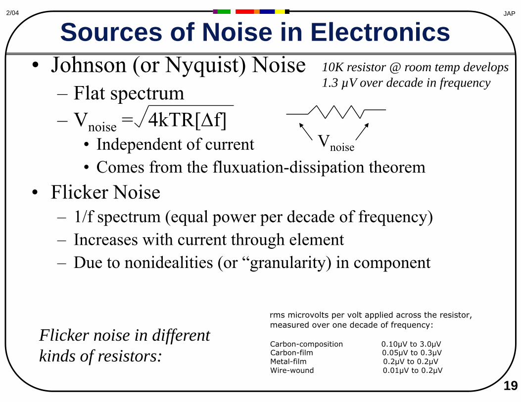
Sources of Noise in Electronics • Johnson (or Nyquist) Noise
– Flat spectrum – Vnoise = 4kTR[Δf]
• Independent of current • Comes from the fluxuation-dissipation theorem
• Flicker Noise – 1/f spectrum (equal power per decade of frequency) – Increases with current through element – Due to nonidealities (or “granularity) in component
Flicker noise in different kinds of resistors:
Vnoise
10K resistor @ room temp develops 1.3 µV over decade in frequency
rms microvolts per volt applied across the resistor, measured over one decade of frequency:
Carbon-composition 0.10µV to 3.0µVCarbon-film 0.05µV to 0.3µVMetal-film 0.2µV to 0.2µVWire-wound 0.01µV to 0.2µV
19
20
JAP2/04
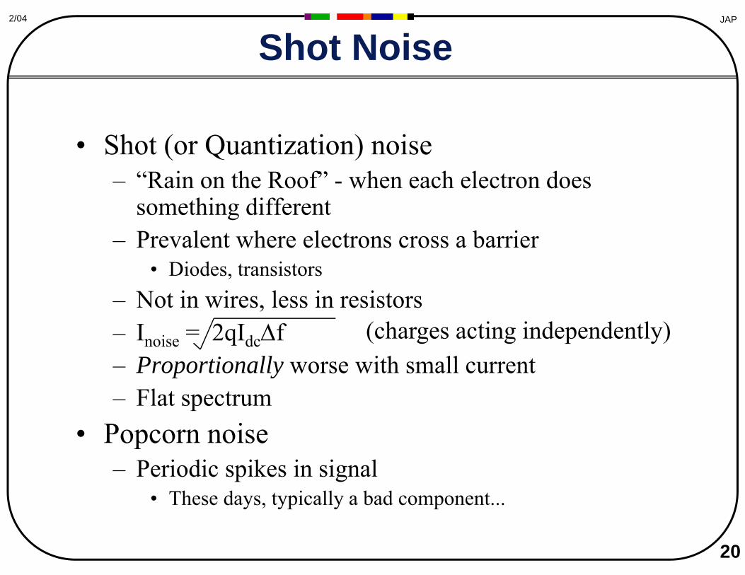
Shot Noise
• Shot (or Quantization) noise – “Rain on the Roof” - when each electron does
something different – Prevalent where electrons cross a barrier
• Diodes, transistors – Not in wires, less in resistors – Inoise = 2qIdcΔf – Proportionally worse with small current – Flat spectrum
• Popcorn noise – Periodic spikes in signal
• These days, typically a bad component...
(charges acting independently)
21
JAP2/04
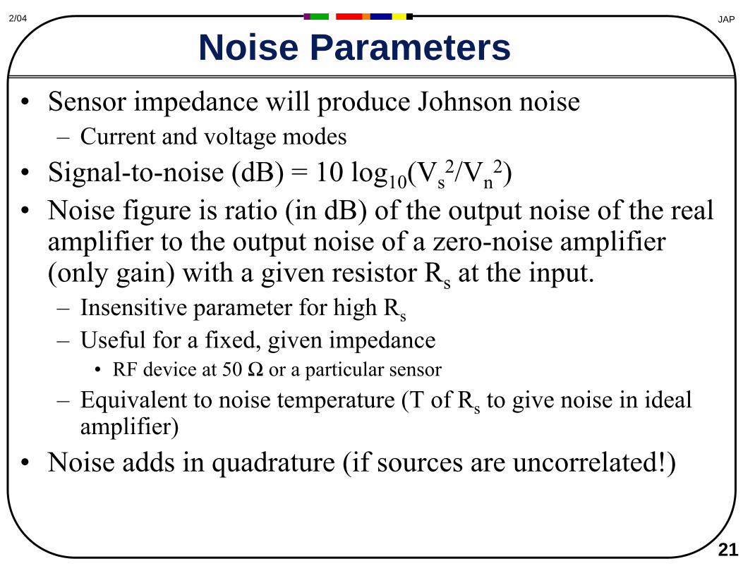
Noise Parameters • Sensor impedance will produce Johnson noise
– Current and voltage modes • Signal-to-noise (dB) = 10 log10(Vs
2/Vn 2)
• Noise figure is ratio (in dB) of the output noise of the real amplifier to the output noise of a zero-noise amplifier (only gain) with a given resistor Rs at the input. – Insensitive parameter for high Rs – Useful for a fixed, given impedance
• RF device at 50 Ω or a particular sensor – Equivalent to noise temperature (T of Rs to give noise in ideal
amplifier) • Noise adds in quadrature (if sources are uncorrelated!)
23
JAP2/04
Noise in Inverting and Noninverting Amplifiers
Noise gain, and the problem with capacitive loads at the inverting input Short answer for noise - for high impedance sources, use low in OpAmps
- for low impedance sources, use low vn OpAmps
Noise gain = noninverting gain via Thevenin
Images from “The Art of Electronics” (page 447) describing noise in non-inverting and inverting amplifiers removed due to copyright restrictions. See: Google Books.
25
JAP2/04
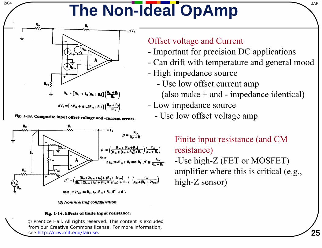
The Non-Ideal OpAmp
Offset voltage and Current - Important for precision DC applications - Can drift with temperature and general mood - High impedance source
- Use low offset current amp (also make + and - impedance identical)
- Low impedance source - Use low offset voltage amp
Finite input resistance (and CM resistance) -Use high-Z (FET or MOSFET) amplifier where this is critical (e.g., high-Z sensor)
© Prentice Hall. All rights reserved. This content is excluded from our Creative Commons license. For more information, see http://ocw.mit.edu/fairuse.
26
JAP2/04
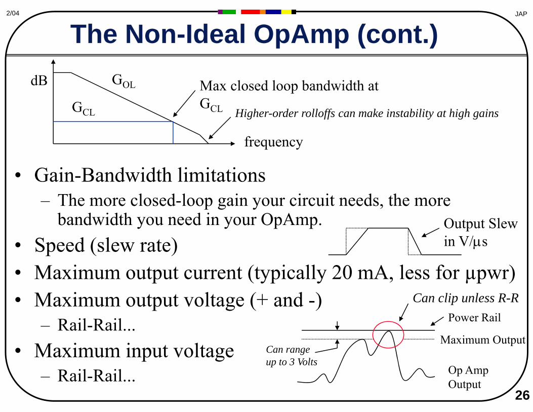
The Non-Ideal OpAmp (cont.)
• Gain-Bandwidth limitations – The more closed-loop gain your circuit needs, the more
bandwidth you need in your OpAmp. Output Slew • Speed (slew rate) • Maximum output current (typically• Maximum output voltage (+ and -)
20 mA, less for µpwr)
– Rail-Rail... • Maximum input voltage
– Rail-Rail...
GOL
GCL
dB Max closed loop bandwidth at GCL
frequency
Higher-order rolloffs can make instability at high gains
in V/μs
Op Amp Output
Power Rail
Maximum Output
Can clip unless R-R
Can range up to 3 Volts
30
JA
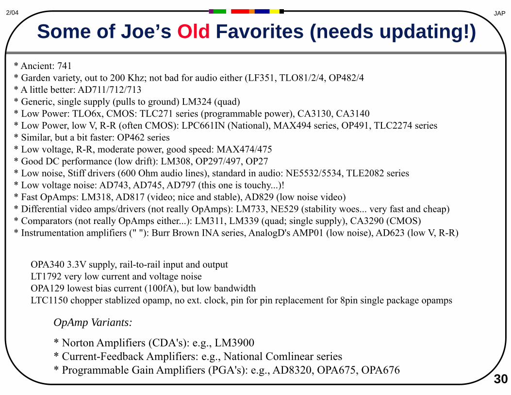
Some of Joe’s Old Favorites (needs updating!) P2/04
* Ancient: 741 * Garden variety, out to 200 Khz; not bad for audio either (LF351, TLO81/2/4, OP482/4 * A little better: AD711/712/713 * Generic, single supply (pulls to ground) LM324 (quad) * Low Power: TLO6x, CMOS: TLC271 series (programmable power), CA3130, CA3140 * Low Power, low V, R-R (often CMOS): LPC661IN (National), MAX494 series, OP491, TLC2274 series * Similar, but a bit faster: OP462 series * Low voltage, R-R, moderate power, good speed: MAX474/475 * Good DC performance (low drift): LM308, OP297/497, OP27 * Low noise, Stiff drivers (600 Ohm audio lines), standard in audio: NE5532/5534, TLE2082 series * Low voltage noise: AD743, AD745, AD797 (this one is touchy...)! * Fast OpAmps: LM318, AD817 (video; nice and stable), AD829 (low noise video) * Differential video amps/drivers (not really OpAmps): LM733, NE529 (stability woes... very fast and cheap) * Comparators (not really OpAmps either...): LM311, LM339 (quad; single supply), CA3290 (CMOS) * Instrumentation amplifiers (" "): Burr Brown INA series, AnalogD's AMP01 (low noise), AD623 (low V, R-R)
OpAmp Variants:
* Norton Amplifiers (CDA's): e.g., LM3900 * Current-Feedback Amplifiers: e.g., National Comlinear series * Programmable Gain Amplifiers (PGA's): e.g., AD8320, OPA675, OPA676
OPA340 3.3V supply, rail-to-rail input and output LT1792 very low current and voltage noise OPA129 lowest bias current (100fA), but low bandwidth LTC1150 chopper stablized opamp, no ext. clock, pin for pin replacement for 8pin single package opamps
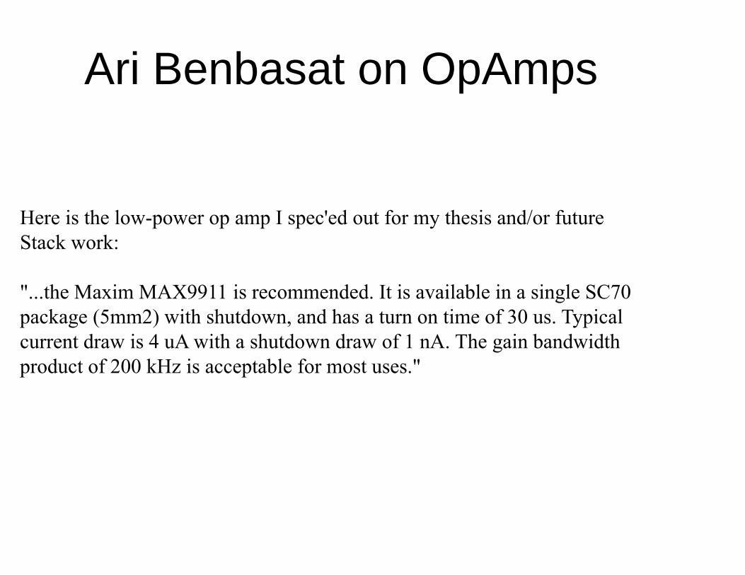
Ari Benbasat on OpAmps
Here is the low-power op amp I spec'ed out for my thesis and/or future Stack work:
"...the Maxim MAX9911 is recommended. It is available in a single SC70 package (5mm2) with shutdown, and has a turn on time of 30 us. Typical current draw is 4 uA with a shutdown draw of 1 nA. The gain bandwidth product of 200 kHz is acceptable for most uses."
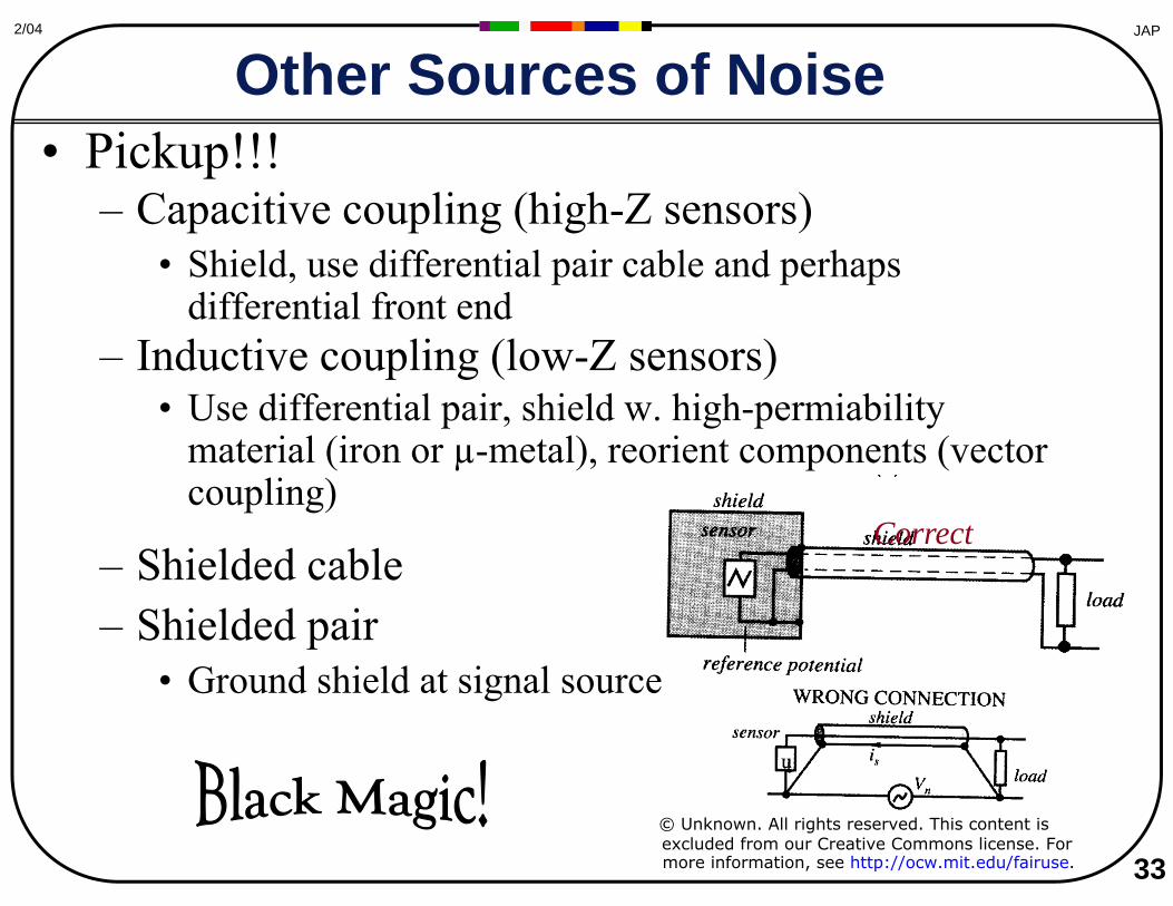
• Pickup!!! – Capacitive coupling (high-Z sensors)
• Shield, use differential pair cable and perhaps differential front end
– Inductive coupling (low-Z sensors) • Use differential pair, shield w. high-permiability
material (iron or µ-metal), reorient components (vector
33
JAP2/04
Other Sources of Noise
coupling)
– Shielded cable – Shielded pair
• Ground shield at signal source
Correct
© Unknown. All rights reserved. This content is excluded from our Creative Commons license. For more information, see http://ocw.mit.edu/fairuse.
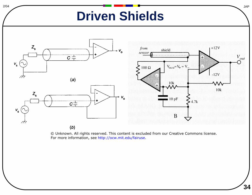
34
JAP2/04
Driven Shields
© Unknown. All rights reserved. This content is excluded from our Creative Commons license. For more information, see http://ocw.mit.edu/fairuse.
35
JAP2/04
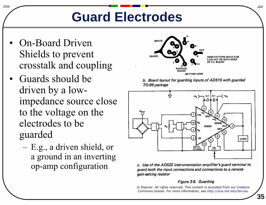
Guard Electrodes
• On-Board Driven Shields to prevent crosstalk and coupling
• Guards should be driven by a low-impedance source close to the voltage on the electrodes to be guarded – E.g., a driven shield, or
a ground in an inverting op-amp configuration
© Elsevier. All rights reserved. This content is excluded from our CreativeCommons license. For more information, see http://ocw.mit.edu/fairuse.
36
JAP2/04
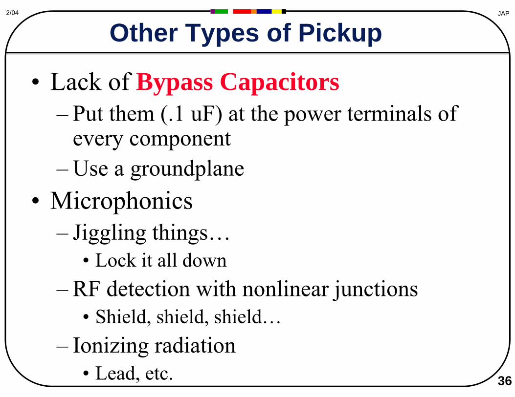
Other Types of Pickup
• Lack of Bypass Capacitors – Put them (.1 uF) at the power terminals of
every component – Use a groundplane
• Microphonics – Jiggling things…
• Lock it all down – RF detection with nonlinear junctions
• Shield, shield, shield… – Ionizing radiation
• Lead, etc.
37
JAP2/04
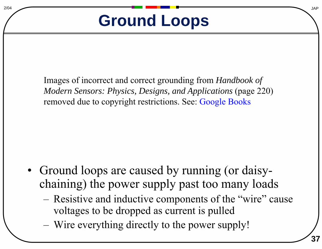
Ground Loops
• Ground loops are caused by running (or daisychaining) the power supply past too many loads – Resistive and inductive components of the “wire” cause
voltages to be dropped as current is pulled – Wire everything directly to the power supply!
Images of incorrect and correct grounding from Handbook of Modern Sensors: Physics, Designs, and Applications (page 220) removed due to copyright restrictions. See: Google Books
JAP2/04
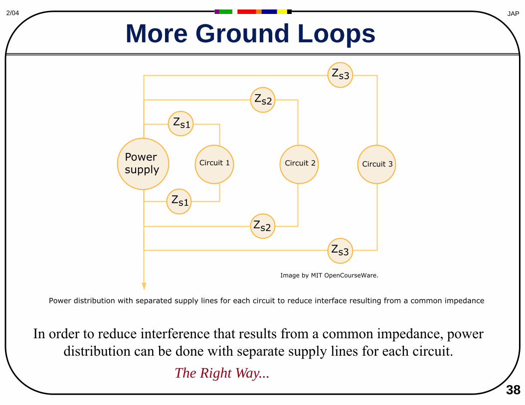
More Ground Loops
In order to reduce interference that results from a common impedance, power distribution can be done with separate supply lines for each circuit.
The Right Way... 38
Power distribution with separated supply lines for each circuit to reduce interface resulting from a common impedance
Zs1
Zs1
Zs2
Zs3
Powersupply
Circuit 1 Circuit 2 Circuit 3
Zs2
Zs3
Powersupply
Image by MIT OpenCourseWare.
40
JAP2/04
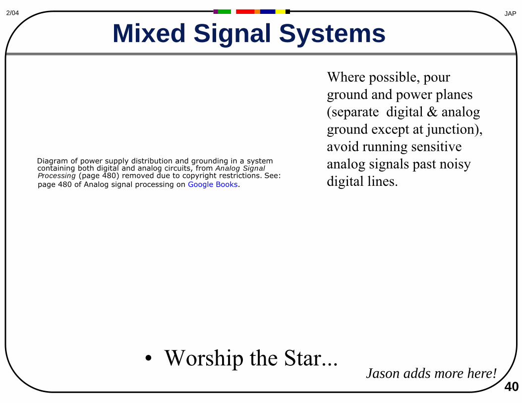
Mixed Signal Systems
• Worship the Star... Jason adds more here!
Where possible, pour ground and power planes (separate digital & analog ground except at junction), avoid running sensitive analog signals past noisy digital lines.
Diagram of power supply distribution and grounding in a system containing both digital and analog circuits, from Analog Signal Processing (page 480) removed due to copyright restrictions. See: page 480 of Analog signal processing on Google Books.
42
JAP2/04
Many books on the subject…
… But it’s often a black art!
Cover for Noise Reduction Techniques in Cover for Grounding and Shielding Electronic Systems, Henry W. Ott, Techniques, Ralph Morrison, removed due
removed due to copyright restrictions. to copyright restrictions.
43
JAP2/04
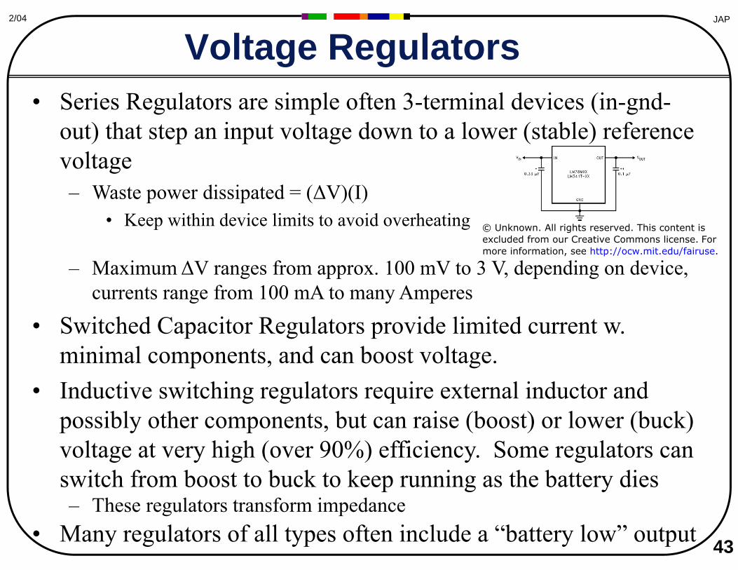
Voltage Regulators • Series Regulators are simple often 3-terminal devices (in-gnd
out) that step an input voltage down to a lower (stable) reference voltage – Waste power dissipated = (ΔV)(I)
• Keep within device limits to avoid overheating
– Maximum ΔV ranges from approx. 100 mV to 3 V, depending on device, currents range from 100 mA to many Amperes
• Switched Capacitor Regulators provide limited current w. minimal components, and can boost voltage.
• Inductive switching regulators require external inductor and possibly other components, but can raise (boost) or lower (buck) voltage at very high (over 90%) efficiency. Some regulators can switch from boost to buck to keep running as the battery dies – These regulators transform impedance
• Many regulators of all types often include a “battery low” output
© Unknown. All rights reserved. This content is excluded from our Creative Commons license. For more information, see http://ocw.mit.edu/fairuse.
45
JAP2/04
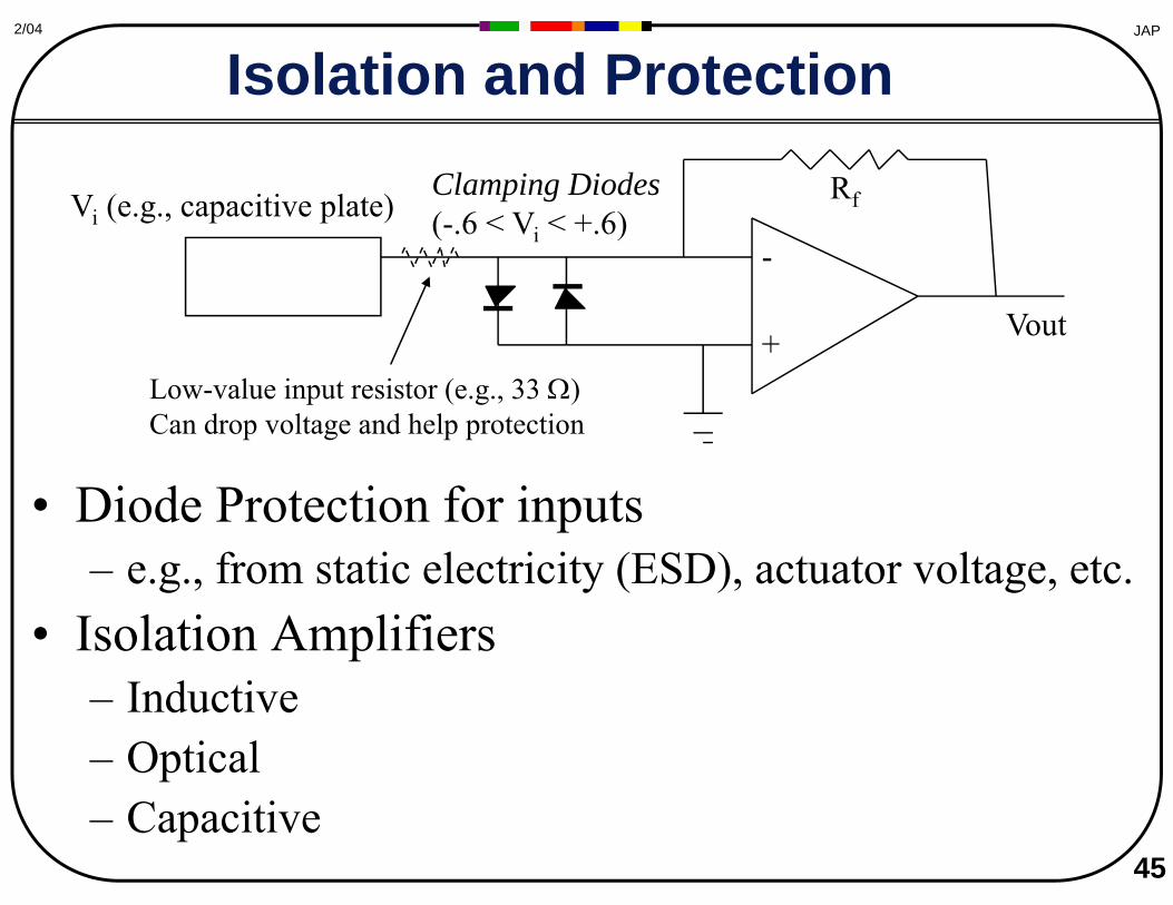
Isolation and Protection
• Diode Protection for inputs – e.g., from static electricity (ESD), actuator voltage, etc.
• Isolation Amplifiers – Inductive – Optical – Capacitive
-
+
Rf
Vout
Vi (e.g., capacitive plate) Clamping Diodes (-.6 < Vi < +.6)
Low-value input resistor (e.g., 33 Ω) Can drop voltage and help protection
46
JAP2/04
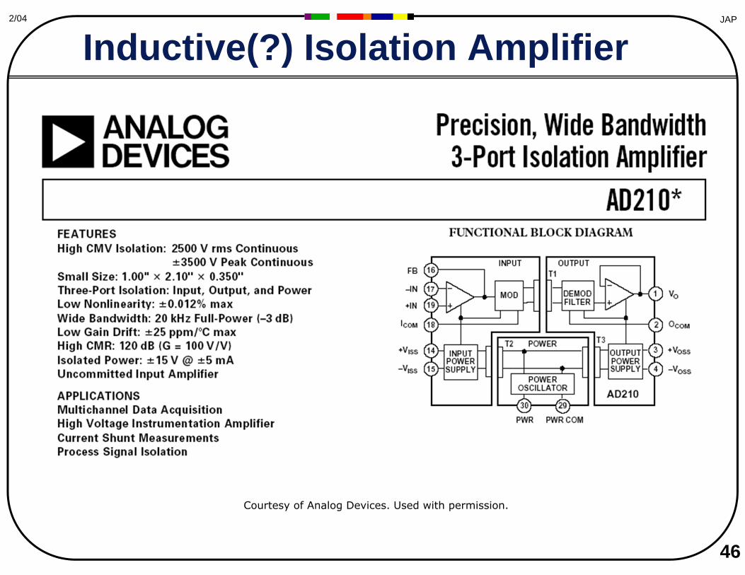
Inductive(?) Isolation Amplifier
Courtesy of Analog Devices. Used with permission.
JAP2/04
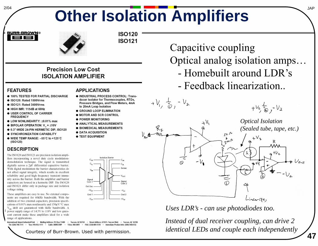
Other Isolation Amplifiers
Capacitive coupling Optical analog isolation amps…
- Homebuilt around LDR’s - Feedback linearization..
Uses LDR’s - can use photodiodes too.
Instead of dual receiver coupling, can drive 2 identical LEDs and couple each independently
47
Optical Isolation (Sealed tube, tape, etc.)
R
Courtesy of Burr-Brown. Used with permission.
MIT OpenCourseWarehttp://ocw.mit.edu
MAS.836 Sensor Technologies for Interactive EnvironmentsSpring 2011
For information about citing these materials or our Terms of Use, visit: http://ocw.mit.edu/terms.

![ΒΙΒΛΙΟΓΡΑΦΙΑ - NTUAusers.ntua.gr/igonos/PDF/Bibliography.pdf · ΒΙΒΛΙΟΓΡΑΦΙΑ 210 [25] Schwarz S.J., “Analytical expressions for the resistance of grounding](https://static.fdocument.org/doc/165x107/5a7597df7f8b9a4b538c9a8a/-ntuausersntuagrigonospdfbibliographypdf-.jpg)