LTC2470/LTC2472 - Selectable 208sps/833sps, 16-Bit ΔΣ …€¦ · · 2018-05-11LTC2470IMS#PBF...
22
LTC2470/LTC2472 1 24702fb For more information www.linear.com/LTC2470 –50 –10 10 –30 50 70 30 90 TEMPERATURE (°C) REFERENCE OUTPUT VOLTAGE (V) 1.2520 1.2515 1.2510 1.2505 1.2500 24702 TA01b 1.2480 1.2485 1.2490 1.2495 TYPICAL APPLICATION FEATURES APPLICATIONS DESCRIPTION Selectable 208sps/833sps, 16-Bit ΔΣ ADCs with 10ppm/°C Max Precision Reference The LTC ® 2470/LTC2472 are small, 16-bit analog-to-digital converters with an integrated precision reference and a selectable 208sps or 833sps output rate. They use a single 2.7V to 5.5V supply and communicate through a SPI Interface. The LTC2470 is single-ended with a 0V to V REF input range and the LTC2472 is differential with a ±V REF input range. Both ADC’s include a 1.25V integrated reference with 2ppm/°C drift performance and 0.1% initial accuracy. The converters are available in a 12-pin DFN 3mm × 3mm package or an MSOP-12 package. They include an integrated oscillator and perform conversions with no latency for multiplexed applications. The LTC2470/ LTC2472 include a proprietary input sampling scheme that reduces the average input current several orders of magnitude when compared to conventional delta sigma converters. Following a single conversion, the LTC2470/LTC2472 automatically power down the converter and can also be configured to power down the reference. When both the ADC and reference are powered down, the supply current is reduced to 200nA. The LTC2470/LTC2472 include a user selectable 208sps or 833sps output rate and due to a large oversampling ratio (8,192 at 208sps and 2,048 at 833sps) have relaxed anti-aliasing requirements. V REF vs Temperature n 16-Bit Resolution n Internal, High Accuracy Reference—10ppm/°C (Max) n Single-Ended (LTC2470) or Differential (LTC2472) n Selectable 208sps/833sps Output Rate n 1mV Offset Error n 0.01% Gain Error n Single Conversion Settling Time for Multiplexed Applications n Single-Cycle Operation with Auto Shutdown n 3.5mA (Typ) Supply Current n 2µA (Max) Sleep Current n Internal Oscillator—No External Components Required n SPI Interface n Small 12-Lead, 3mm × 3mm DFN and MSOP Packages n System Monitoring n Environmental Monitoring n Direct Temperature Measurements n Instrumentation n Industrial Process Control n Data Acquisition n Embedded ADC Upgrades L, LT, LTC, LTM, Linear Technology and the Linear logo are registered trademarks and No Latency ∆∑ is a trademark of Linear Technology Corporation. All other trademarks are the property of their respective owners. Protected by U.S. Patents, including 6208279, 6411242, 7088280, 7164378. 10k 10k 10k R SCK SPI INTERFACE SDO CS 0.1μF 0.1μF 2.7V TO 5.5V 10μF 0.1μF IN + REFOUT REF – V CC 0.1μF COMP GND IN – 0.1μF LTC2472 24702 TA01a
-
Upload
trankhuong -
Category
Documents
-
view
217 -
download
1
Transcript of LTC2470/LTC2472 - Selectable 208sps/833sps, 16-Bit ΔΣ …€¦ · · 2018-05-11LTC2470IMS#PBF...
LTC2470/LTC2472
124702fb
For more information www.linear.com/LTC2470
–50 –10 10–30 50 7030 90TEMPERATURE (°C)
REFE
RENC
E OU
TPUT
VOL
TAGE
(V)
1.2520
1.2515
1.2510
1.2505
1.2500
24702 TA01b
1.2480
1.2485
1.2490
1.2495
Typical applicaTion
FeaTures
applicaTions
DescripTion
Selectable 208sps/833sps, 16-Bit ΔΣ ADCs with 10ppm/°C
Max Precision Reference
The LTC®2470/LTC2472 are small, 16-bit analog-to-digital converters with an integrated precision reference and a selectable 208sps or 833sps output rate. They use a single 2.7V to 5.5V supply and communicate through a SPI Interface. The LTC2470 is single-ended with a 0V to VREF input range and the LTC2472 is differential with a ±VREF input range. Both ADC’s include a 1.25V integrated reference with 2ppm/°C drift performance and 0.1% initial accuracy. The converters are available in a 12-pin DFN 3mm × 3mm package or an MSOP-12 package. They include an integrated oscillator and perform conversions with no latency for multiplexed applications. The LTC2470/ LTC2472 include a proprietary input sampling scheme that reduces the average input current several orders of magnitude when compared to conventional delta sigma converters.
Following a single conversion, the LTC2470/LTC2472 automatically power down the converter and can also be configured to power down the reference. When both the ADC and reference are powered down, the supply current is reduced to 200nA.
The LTC2470/LTC2472 include a user selectable 208sps or 833sps output rate and due to a large oversampling ratio (8,192 at 208sps and 2,048 at 833sps) have relaxed anti-aliasing requirements.
VREF vs Temperature
n 16-Bit Resolution n Internal, High Accuracy Reference—10ppm/°C (Max) n Single-Ended (LTC2470) or Differential (LTC2472) n Selectable 208sps/833sps Output Rate n 1mV Offset Error n 0.01% Gain Error n Single Conversion Settling Time for Multiplexed
Applications n Single-Cycle Operation with Auto Shutdown n 3.5mA (Typ) Supply Current n 2µA (Max) Sleep Current n Internal Oscillator—No External Components
Required n SPI Interface n Small 12-Lead, 3mm × 3mm DFN and MSOP
Packages
n System Monitoring n Environmental Monitoring n Direct Temperature Measurements n Instrumentation n Industrial Process Control n Data Acquisition n Embedded ADC Upgrades L, LT, LTC, LTM, Linear Technology and the Linear logo are registered trademarks and No Latency ∆∑ is a trademark of Linear Technology Corporation. All other trademarks are the property of their respective owners. Protected by U.S. Patents, including 6208279, 6411242, 7088280, 7164378.
10k
10k
10k
R
SCKSPIINTERFACESDO
CS
0.1µF
0.1µF
2.7V TO 5.5V
10µF
0.1µF
IN+
REFOUT
REF–
VCC
0.1µF
COMP
GND
IN–
0.1µF
LTC2472
24702 TA01a
LTC2470/LTC2472
224702fb
For more information www.linear.com/LTC2470
pin conFiguraTion
absoluTe MaxiMuM raTings
Supply Voltage (VCC) ................................... –0.3V to 6VAnalog Input Voltage (VIN
+, VIN–, VIN, VREF
–, VCOMP, VREFOUT) ...........................–0.3V to (VCC + 0.3V)Digital Voltage (VSDI, VSDO, VSCK, VCS) ................–0.3V to (VCC + 0.3V)
(Notes 1, 2)
orDer inForMaTion
Storage Temperature Range .................. –65°C to 150°COperating Temperature Range
LTC2470C/LTC2472C ............................... 0°C to 70°C LTC2470I/LTC2472I .............................–40°C to 85°C
LTC2472 LTC2472
TOP VIEW
DD PACKAGE12-LEAD (3mm × 3mm) PLASTIC DFN
12
11
8
9
104
5
3
2
1 VCC
GND
IN–
IN+
REF–
GND
REFOUT
COMP
CS
SDI
SCK
SDO 6 7
13GND
TJMAX = 125°C, θJA = 43°C/W
EXPOSED PAD (PIN 13) PCB GROUND CONNECTION OPTIONAL
123456
REFOUTCOMP
CSSDISCKSDO
121110987
VCCGNDIN–
IN+
REF–
GND
TOP VIEW
MS PACKAGE12-LEAD PLASTIC MSOP
TJMAX = 125°C, θJA = 130°C/W
LTC2470 LTC2470
TOP VIEW
DD PACKAGE12-LEAD (3mm × 3mm) PLASTIC DFN
12
11
8
9
104
5
3
2
1 VCC
GND
GND
IN
REF–
GND
REFOUT
COMP
CS
SDI
SCK
SDO 6 7
13GND
TJMAX = 125°C, θJA = 43°C/W
EXPOSED PAD (PIN 13) PCB GROUND CONNECTION OPTIONAL
123456
REFOUTCOMP
CSSDISCKSDO
121110987
VCCGNDGNDINREF–
GND
TOP VIEW
MS PACKAGE12-LEAD PLASTIC MSOP
TJMAX = 125°C, θJA = 130°C/W
LEAD FREE FINISH TAPE AND REEL PART MARKING* PACKAGE DESCRIPTION TEMPERATURE RANGELTC2470CDD#PBF LTC2470CDD#TRPBF LFPV 12-Lead Plastic (3mm × 3mm) DFN 0°C to 70°CLTC2470IDD#PBF LTC2470IDD#TRPBF LFPV 12-Lead Plastic (3mm × 3mm) DFN –40°C to 85°CLTC2470CMS#PBF LTC2470CMS#TRPBF 2470 12-Lead Plastic MSOP 0°C to 70°CLTC2470IMS#PBF LTC2470IMS#TRPBF 2470 12-Lead Plastic MSOP –40°C to 85°CLTC2472CDD#PBF LTC2472CDD#TRPBF LFGV 12-Lead Plastic (3mm × 3mm) DFN 0°C to 70°CLTC2472IDD#PBF LTC2472IDD#TRPBF LFGV 12-Lead Plastic (3mm × 3mm) DFN –40°C to 85°C
LTC2470/LTC2472
324702fb
For more information www.linear.com/LTC2470
elecTrical characTerisTicsPARAMETER CONDITIONS MIN TYP MAX UNITS
Resolution 16 Bits
Integral Nonlinearity Output Rate 208sps (Note 4) Output Rate 833sps (Note 4)
l
l
2 8
8.5 16
LSB LSB
Offset Error l ±1 ±2.5 mV
Offset Error Drift 0.05 LSB/°C
Gain Error l ±0.01 ±0.25 % of FS
Gain Error Drift l 0.15 LSB/°C
Transition Noise 3 µVRMS
Power Supply Rejection DC 80 dB
The l denotes the specifications which apply over the full operating temperature range, otherwise specifications are at TA = 25°C. (Note 2)
analog inpuTs The l denotes the specifications which apply over the full operating temperature range, otherwise specifications are at TA = 25°C.SYMBOL PARAMETER CONDITIONS MIN TYP MAX UNITS
VIN+ Positive Input Voltage Range LTC2472 l 0 VREF V
VIN– Negative Input Voltage Range LTC2472 l 0 VREF V
VIN Input Voltage Range LTC2470 l 0 VREF V
VOR+, VUR
+ Overrange/Underrange Voltage, IN+ VIN– = 0.625V 8 LSB
VOR–, VUR
– Overrange/Underrange Voltage, IN– VIN+ = 0.625V 8 LSB
CIN IN+, IN–, IN Sampling Capacitance 0.35 pF
IDC_LEAK(IN+, IN–, IN) IN+, IN– DC Leakage Current (LTC2472) IN DC Leakage Current (LTC2470)
VIN = GND (Note 5) VIN = VCC (Note 5)
l
l
–10 –10
±1 ±1
10 10
nA nA
ICONV Input Sampling Current (Note 8) 50 nA
VREF Reference Output Voltage l 1.247 1.25 1.253 V
Reference Voltage Coefficient (Note 9) C-Grade I-Grade
l
±2 ±5
±10
ppm/°C ppm/°C
Reference Line Regulation 2.7V ≤ VCC ≤ 5.5V –90 dB
Reference Short Circuit Current VCC = 5.5, Forcing Output to GND l 35 mA
COMP Pin Short Circuit Current VCC = 5.5, Forcing Output to GND l 200 µA
Reference Load Regulation 2.7V ≤ VCC ≤ 5.5V, IOUT = 100μA Sourcing 3.5 mV/mA
Reference Output Noise Density CCOMP= 0.1μF, CREFOUT = 0.1μF, At f = 1ksps
30 nV/√Hz
orDer inForMaTionLEAD FREE FINISH TAPE AND REEL PART MARKING* PACKAGE DESCRIPTION TEMPERATURE RANGELTC2472CMS#PBF LTC2472CMS#TRPBF 2472 12-Lead Plastic MSOP 0°C to 70°CLTC2472IMS#PBF LTC2472IMS#TRPBF 2472 12-Lead Plastic MSOP –40°C to 85°C
Consult LTC Marketing for parts specified with wider operating temperature ranges. *The temperature grade is identified by a label on the shipping container. Consult LTC Marketing for information on non-standard lead based finish parts.For more information on lead free part marking, go to: http://www.linear.com/leadfree/ For more information on tape and reel specifications, go to: http://www.linear.com/tapeandreel/
LTC2470/LTC2472
424702fb
For more information www.linear.com/LTC2470
The l denotes the specifications which apply over the full operating temperature range, otherwise specifications are at TA = 25°C.
SYMBOL PARAMETER CONDITIONS MIN TYP MAX UNITS
tCONV1 Conversion Time SPD = 0 l 3.2 4 4.8 ms
tCONV2 Conversion Time SPD = 1 l 0.8 1 1.2 ms
fSCK SCK Frequency Range l 2 MHz
tlSCK SCK Low Period (Note 7) l 250 ns
thSCK SCK High Period (Note 7) l 250 ns
t1 CS Falling Edge to SDO Low Z (Note 7) l 0 100 ns
t2 CS Rising Edge to SDO High Z (Note 7) l 0 100 ns
t3 CS Falling Edge to SCK Falling Edge (Note 7) l 100 ns
t4 SDI Setup Before SCK↑ (Notes 3, 7) l 100 ns
t5 SDI Hold After SCK↑ (Notes 3, 7) l 100 ns
tKQ SCK Falling Edge to SDO Valid (Note 7) l 0 100 ns
Note 1: Stresses beyond those listed under Absolute Maximum Ratings may cause permanent damage to the device. Exposure to any Absolute Maximum Rating condition for extended periods may affect device reliability and lifetime.Note 2. All voltage values are with respect to GND. VCC = 2.7V to 5.5V unless otherwise specified. VREFCM = VREF/2, FS = VREF, –VREF ≤ VIN ≤ VREF VIN = VIN
+ – VIN–, VINCM = (VIN
+ + VIN–)/2. (LTC2472)
Note 3. Guaranteed by design, not subject to test.Note 4. Integral nonlinearity is defined as the deviation of a code from a straight line passing through the actual endpoints of the transfer curve.
Note 5: CS = VCC. A positive current is flowing into the DUT pin.Note 6: SCK = VCC or GND. SDO is high impedance.Note 7: See Figure 5.Note 8: Input sampling current is the average input current drawn from the input sampling network while the LTC2470/LTC2472 is actively sampling the input.Note 9: Temperature coefficient is calculated by dividing the maximum change in output voltage by the specified temperature range.
TiMing characTerisTics
The l denotes the specifications which apply over the full operating temperature range, otherwise specifications are at TA = 25°C. (Note 2)
SYMBOL PARAMETER CONDITIONS MIN TYP MAX UNITS
VIH High Level Input Voltage l VCC – 0.3 V
VIL Low Level Input Voltage l 0.3 V
IIN Digital Input Current l –10 10 µA
CIN Digital Input Capacitance 10 pF
VOH High Level Output Voltage IO = –800µA l VCC – 0.5 V
VOL Low Level Output Voltage IO = 1.6mA l 0.4 V
IOZ Hi-Z Output Leakage Current l –10 10 µA
DigiTal inpuTs anD DigiTal ouTpuTs
SYMBOL PARAMETER CONDITIONS MIN TYP MAX UNITS
VCC Supply Voltage l 2.7 5.5 V
ICC Supply Current Conversion Conversion Nap Sleep
CS = GND (Note 6) LTC2472 CS = GND (Note 6) LTC2470 CS = VCC (Note 6) CS = VCC (Note 6)
l
l
l
l
3.5 2.5 800 0.2
5 4
1500 2
mA mA µA µA
The l denotes the specifications which apply over the full operating temperature range, otherwise specifications are at TA = 25°C.power requireMenTs
LTC2470/LTC2472
524702fb
For more information www.linear.com/LTC2470
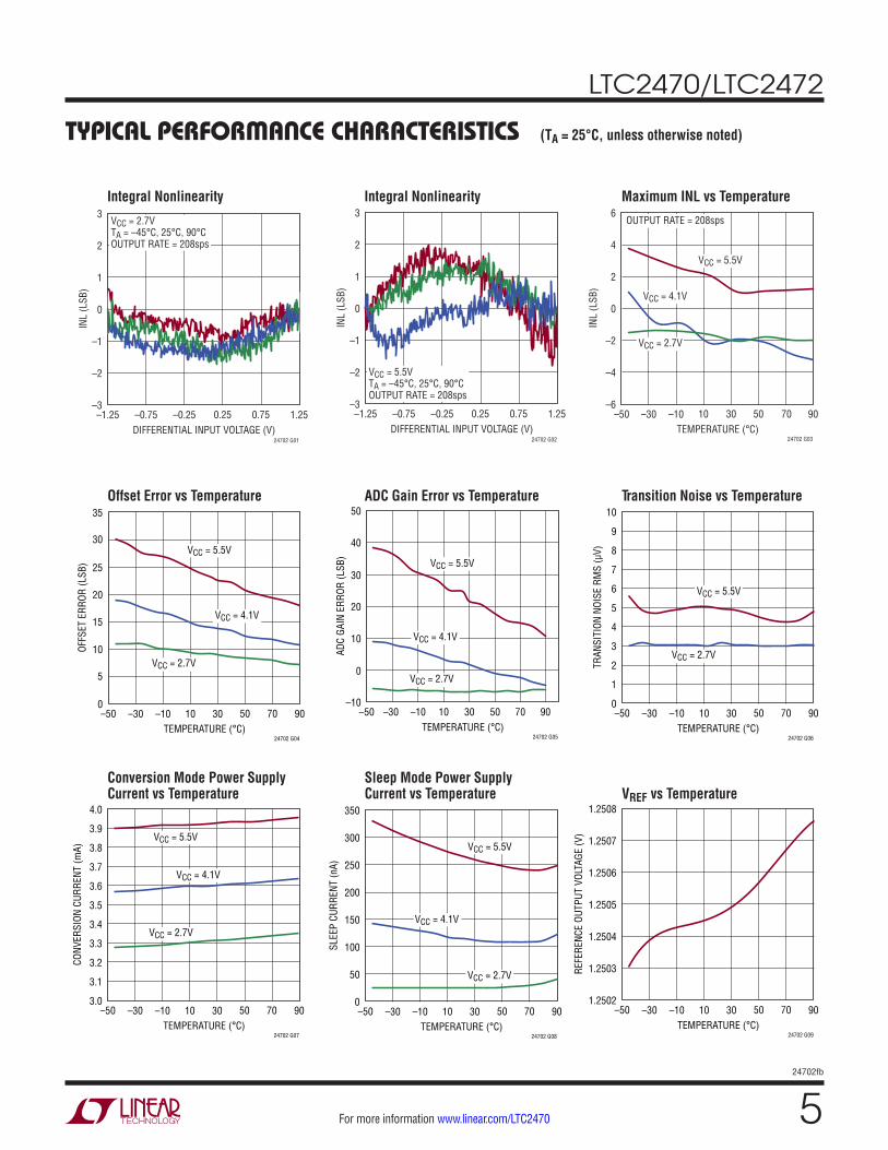
Typical perForMance characTerisTics
Offset Error vs Temperature
ADC Gain Error vs Temperature
Transition Noise vs Temperature
Conversion Mode Power Supply Current vs Temperature
Sleep Mode Power Supply Current vs Temperature
VREF vs Temperature
(TA = 25°C, unless otherwise noted)
TEMPERATURE (°C)
OFFS
ET E
RROR
(LSB
)
15
35
24702 G04
10
20
25
30
5
0
VCC = 5.5V
VCC = 4.1V
VCC = 2.7V
–50 –10 10–30 50 7030 90TEMPERATURE (°C)
–50
ADC
GAIN
ERR
OR (L
SB)
50
0
24702 G05
–10
30
10
20
40
–30 30 50 7010–10 90
VCC = 5.5V
VCC = 4.1V
VCC = 2.7V
TEMPERATURE (°C)
TRAN
SITI
ON N
OISE
RM
S (µ
V)6
10
24702 G06
4
5
7
8
9
3
2
1
0–50 –10 10–30 50 7030 90
VCC = 5.5V
VCC = 2.7V
–50 –10 10–30 50 7030 90
VCC = 5.5V
VCC = 2.7V
TEMPERATURE (°C)
CONV
ERSI
ON C
URRE
NT (m
A)
4.0
3.9
24702 G07
3.4
3.5
3.6
3.7
3.8
3.3
3.2
3.1
3.0
VCC = 4.1V
–50 –10 10–30 50 7030 90
VCC = 5.5V
TEMPERATURE (°C)
SLEE
P CU
RREN
T (n
A)
350
24702 G08
150
300
250
200
100
50
0
VCC = 2.7V
VCC = 4.1V
–50 –10 10–30 50 7030 90TEMPERATURE (°C)
REFE
RENC
E OU
TPUT
VOL
TAGE
(V)
1.2508
24702 G09
1.2502
1.2503
1.2504
1.2505
1.2506
1.2507
Integral Nonlinearity
Integral Nonlinearity
Maximum INL vs Temperature
DIFFERENTIAL INPUT VOLTAGE (V)–1.25 –0.75 –0.25
INL
(LSB
)
1
3
24702 G01
–1
0
2
–2
–30.25 0.75 1.25
VCC = 2.7VTA = –45°C, 25°C, 90°COUTPUT RATE = 208sps
DIFFERENTIAL INPUT VOLTAGE (V)–1.25 –0.75 –0.25
INL
(LSB
)
1
3
24702 G02
–1
0
2
–2
–30.25 0.75 1.25
VCC = 5.5VTA = –45°C, 25°C, 90°COUTPUT RATE = 208sps
TEMPERATURE (°C)
INL
(LSB
)
2
6
24702 G03
–2
0
4
–4
–6–50 –30 10 30 50 70–10 90
VCC = 5.5V
VCC = 4.1V
VCC = 2.7V
OUTPUT RATE = 208sps
LTC2470/LTC2472
624702fb
For more information www.linear.com/LTC2470
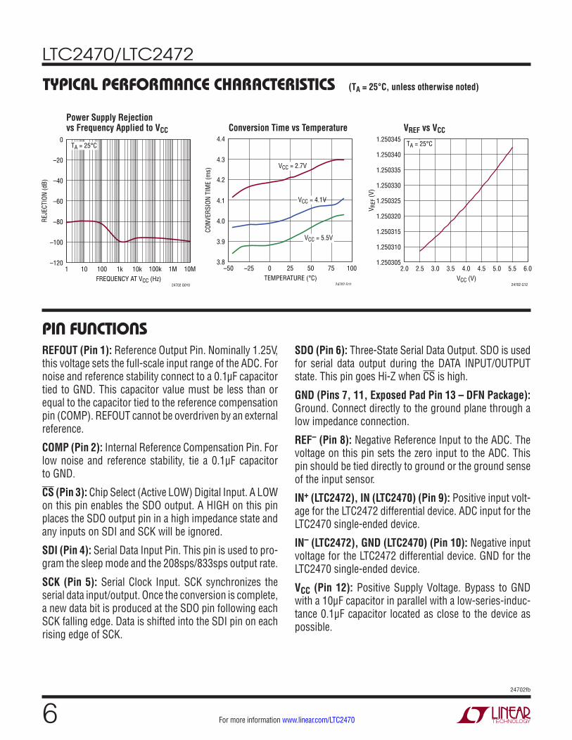
pin FuncTionsREFOUT (Pin 1): Reference Output Pin. Nominally 1.25V, this voltage sets the full-scale input range of the ADC. For noise and reference stability connect to a 0.1µF capacitor tied to GND. This capacitor value must be less than or equal to the capacitor tied to the reference compensation pin (COMP). REFOUT cannot be overdriven by an external reference.
COMP (Pin 2): Internal Reference Compensation Pin. For low noise and reference stability, tie a 0.1μF capacitor to GND.
CS (Pin 3): Chip Select (Active LOW) Digital Input. A LOW on this pin enables the SDO output. A HIGH on this pin places the SDO output pin in a high impedance state and any inputs on SDI and SCK will be ignored.
SDI (Pin 4): Serial Data Input Pin. This pin is used to pro-gram the sleep mode and the 208sps/833sps output rate.
SCK (Pin 5): Serial Clock Input. SCK synchronizes the serial data input/output. Once the conversion is complete, a new data bit is produced at the SDO pin following each SCK falling edge. Data is shifted into the SDI pin on each rising edge of SCK.
SDO (Pin 6): Three-State Serial Data Output. SDO is used for serial data output during the DATA INPUT/OUTPUT state. This pin goes Hi-Z when CS is high.
GND (Pins 7, 11, Exposed Pad Pin 13 – DFN Package): Ground. Connect directly to the ground plane through a low impedance connection.
REF– (Pin 8): Negative Reference Input to the ADC. The voltage on this pin sets the zero input to the ADC. This pin should be tied directly to ground or the ground sense of the input sensor.
IN+ (LTC2472), IN (LTC2470) (Pin 9): Positive input volt-age for the LTC2472 differential device. ADC input for the LTC2470 single-ended device.
IN– (LTC2472), GND (LTC2470) (Pin 10): Negative input voltage for the LTC2472 differential device. GND for the LTC2470 single-ended device.
VCC (Pin 12): Positive Supply Voltage. Bypass to GND with a 10μF capacitor in parallel with a low-series-induc-tance 0.1μF capacitor located as close to the device as possible.
Typical perForMance characTerisTics (TA = 25°C, unless otherwise noted)
Power Supply Rejection vs Frequency Applied to VCC
Conversion Time vs Temperature
10 100 1k1 100k 1M10k 10MFREQUENCY AT VCC (Hz)
REJE
CTIO
N (d
B)
0
24702 G010
–120
–100
–80
–60
–40
–20
TA = 25°C
TEMPERATURE (°C)–50
CONV
ERSI
ON T
IME
(ms)
24702 G11
4.4
4.0
4.1
4.2
4.3
3.9
3.8–25 25 50 750 100
VCC = 2.7V
VCC = 4.1V
VCC = 5.5V
VREF vs VCC
2.0 3.52.5 4.03.0 5.0 5.54.5 6.0VCC (V)
V REF
(V)
1.250345
1.250340
24702 G12
1.250305
1.250310
1.250315
1.250320
1.250325
1.250330
1.250335
TA = 25°C
LTC2470/LTC2472
724702fb
For more information www.linear.com/LTC2470
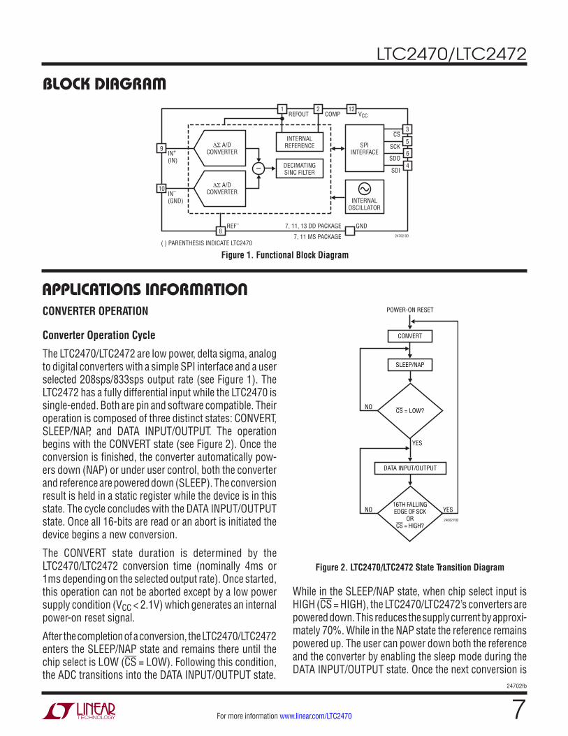
applicaTions inForMaTionCONVERTER OPERATION
Converter Operation Cycle
The LTC2470/LTC2472 are low power, delta sigma, analog to digital converters with a simple SPI interface and a user selected 208sps/833sps output rate (see Figure 1). The LTC2472 has a fully differential input while the LTC2470 is single-ended. Both are pin and software compatible. Their operation is composed of three distinct states: CONVERT, SLEEP/NAP, and DATA INPUT/OUTPUT. The operation begins with the CONVERT state (see Figure 2). Once the conversion is finished, the converter automatically pow-ers down (NAP) or under user control, both the converter and reference are powered down (SLEEP). The conversion result is held in a static register while the device is in this state. The cycle concludes with the DATA INPUT/OUTPUT state. Once all 16-bits are read or an abort is initiated the device begins a new conversion.
The CONVERT state duration is determined by the LTC2470/LTC2472 conversion time (nominally 4ms or 1ms depending on the selected output rate). Once started, this operation can not be aborted except by a low power supply condition (VCC < 2.1V) which generates an internal power-on reset signal.
After the completion of a conversion, the LTC2470/LTC2472 enters the SLEEP/NAP state and remains there until the chip select is LOW (CS = LOW). Following this condition, the ADC transitions into the DATA INPUT/OUTPUT state.
Figure 2. LTC2470/LTC2472 State Transition Diagram
While in the SLEEP/NAP state, when chip select input is HIGH (CS = HIGH), the LTC2470/LTC2472’s converters are powered down. This reduces the supply current by approxi-mately 70%. While in the NAP state the reference remains powered up. The user can power down both the reference and the converter by enabling the sleep mode during the DATA INPUT/OUTPUT state. Once the next conversion is
DATA INPUT/OUTPUT
SLEEP/NAP
CONVERT
POWER-ON RESET
YES
24602 F02
16TH FALLINGEDGE OF SCK
ORCS = HIGH?
CS = LOW?
NO YES
NO
block DiagraM
Figure 1. Functional Block Diagram
ΔΣ A/DCONVERTER
DECIMATINGSINC FILTER
SDO
REFOUT COMP
REF–
IN+
(IN)
IN–
(GND)
SCK
CS
24702 BD
–
ΔΣ A/DCONVERTER
INTERNALREFERENCE
( ) PARENTHESIS INDICATE LTC2470
SPIINTERFACE
INTERNALOSCILLATOR
1VCC
122
3
5
6
SDI4
8GND7, 11, 13 DD PACKAGE
7, 11 MS PACKAGE
9
10
LTC2470/LTC2472
824702fb
For more information www.linear.com/LTC2470
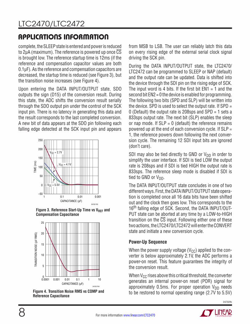
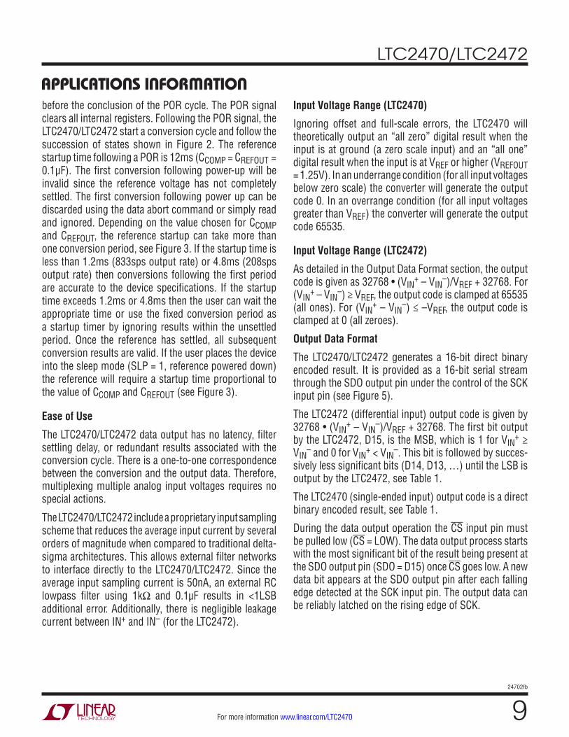
applicaTions inForMaTioncomplete, the SLEEP state is entered and power is reduced to 2μA (maximum). The reference is powered up once CS is brought low. The reference startup time is 12ms (if the reference and compensation capacitor values are both 0.1μF). As the reference and compensation capacitors are decreased, the startup time is reduced (see Figure 3), but the transition noise increases (see Figure 4).
Upon entering the DATA INPUT/OUTPUT state, SDO outputs the sign (D15) of the conversion result. During this state, the ADC shifts the conversion result serially through the SDO output pin under the control of the SCK input pin. There is no latency in generating this data and the result corresponds to the last completed conversion. A new bit of data appears at the SDO pin following each falling edge detected at the SCK input pin and appears
from MSB to LSB. The user can reliably latch this data on every rising edge of the external serial clock signal driving the SCK pin.
During the DATA INPUT/OUTPUT state, the LTC2470/LTC2472 can be programmed to SLEEP or NAP (default) and the output rate can be updated. Data is shifted into the device through the SDI pin on the rising edge of SCK. The input word is 4 bits. If the first bit EN1 = 1 and the second bit EN2 = 0 the device is enabled for programming. The following two bits (SPD and SLP) will be written into the device. SPD is used to select the output rate. If SPD = 0 (Default) the output rate is 208sps and SPD = 1 sets a 833sps output rate. The next bit (SLP) enables the sleep or nap mode. If SLP = 0 (default) the reference remains powered up at the end of each conversion cycle. If SLP = 1, the reference powers down following the next conver-sion cycle. The remaining 12 SDI input bits are ignored (don’t care).
SDI may also be tied directly to GND or VDD in order to simplify the user interface. If SDI is tied LOW the output rate is 208sps and if SDI is tied HIGH the output rate is 833sps. The reference sleep mode is disabled if SDI is tied to GND or VDD.
The DATA INPUT/OUTPUT state concludes in one of two different ways. First, the DATA INPUT/OUTPUT state opera-tion is completed once all 16 data bits have been shifted out and the clock then goes low. This corresponds to the 16th falling edge of SCK. Second, the DATA INPUT/OUT-PUT state can be aborted at any time by a LOW-to-HIGH transition on the CS input. Following either one of these two actions, the LTC2470/LTC2472 will enter the CONVERT state and initiate a new conversion cycle.
Power-Up Sequence
When the power supply voltage (VCC) applied to the con-verter is below approximately 2.1V, the ADC performs a power-on reset. This feature guarantees the integrity of the conversion result.
When VCC rises above this critical threshold, the converter generates an internal power-on reset (POR) signal for approximately 0.5ms. For proper operation VDD needs to be restored to normal operating range (2.7V to 5.5V) Figure 4. Transition Noise RMS vs COMP and
Reference Capacitance
Figure 3. Reference Start-Up Time vs VREF and Compensation Capacitance
CAPACITANCE (µF)1
TIM
E (m
s)
50
150
250
24702 F03
–50
0
100
200
0.1 0.01 0.001
VCC = 5.5V
VCC = 4.1V
VCC = 2.7V
0.001 0.01 0.10.0001 101CAPACITANCE (µF)
TRAN
SITI
ON N
OISE
(µV
RMS)
24702 F04
0
5
10
15
20
25
LTC2470/LTC2472
924702fb
For more information www.linear.com/LTC2470
before the conclusion of the POR cycle. The POR signal clears all internal registers. Following the POR signal, the LTC2470/LTC2472 start a conversion cycle and follow the succession of states shown in Figure 2. The reference startup time following a POR is 12ms (CCOMP = CREFOUT = 0.1μF). The first conversion following power-up will be invalid since the reference voltage has not completely settled. The first conversion following power up can be discarded using the data abort command or simply read and ignored. Depending on the value chosen for CCOMP and CREFOUT, the reference startup can take more than one conversion period, see Figure 3. If the startup time is less than 1.2ms (833sps output rate) or 4.8ms (208sps output rate) then conversions following the first period are accurate to the device specifications. If the startup time exceeds 1.2ms or 4.8ms then the user can wait the appropriate time or use the fixed conversion period as a startup timer by ignoring results within the unsettled period. Once the reference has settled, all subsequent conversion results are valid. If the user places the device into the sleep mode (SLP = 1, reference powered down) the reference will require a startup time proportional to the value of CCOMP and CREFOUT (see Figure 3).
Ease of Use
The LTC2470/LTC2472 data output has no latency, filter settling delay, or redundant results associated with the conversion cycle. There is a one-to-one correspondence between the conversion and the output data. Therefore, multiplexing multiple analog input voltages requires no special actions.
The LTC2470/LTC2472 include a proprietary input sampling scheme that reduces the average input current by several orders of magnitude when compared to traditional delta-sigma architectures. This allows external filter networks to interface directly to the LTC2470/LTC2472. Since the average input sampling current is 50nA, an external RC lowpass filter using 1kΩ and 0.1µF results in <1LSB additional error. Additionally, there is negligible leakage current between IN+ and IN– (for the LTC2472).
Input Voltage Range (LTC2470)
Ignoring offset and full-scale errors, the LTC2470 will theoretically output an “all zero” digital result when the input is at ground (a zero scale input) and an “all one” digital result when the input is at VREF or higher (VREFOUT = 1.25V). In an underrange condition (for all input voltages below zero scale) the converter will generate the output code 0. In an overrange condition (for all input voltages greater than VREF) the converter will generate the output code 65535.
Input Voltage Range (LTC2472)
As detailed in the Output Data Format section, the output code is given as 32768 • (VIN
+ – VIN–)/VREF + 32768. For
(VIN+ – VIN
–) ≥ VREF, the output code is clamped at 65535 (all ones). For (VIN
+ – VIN–) ≤ –VREF, the output code is
clamped at 0 (all zeroes).
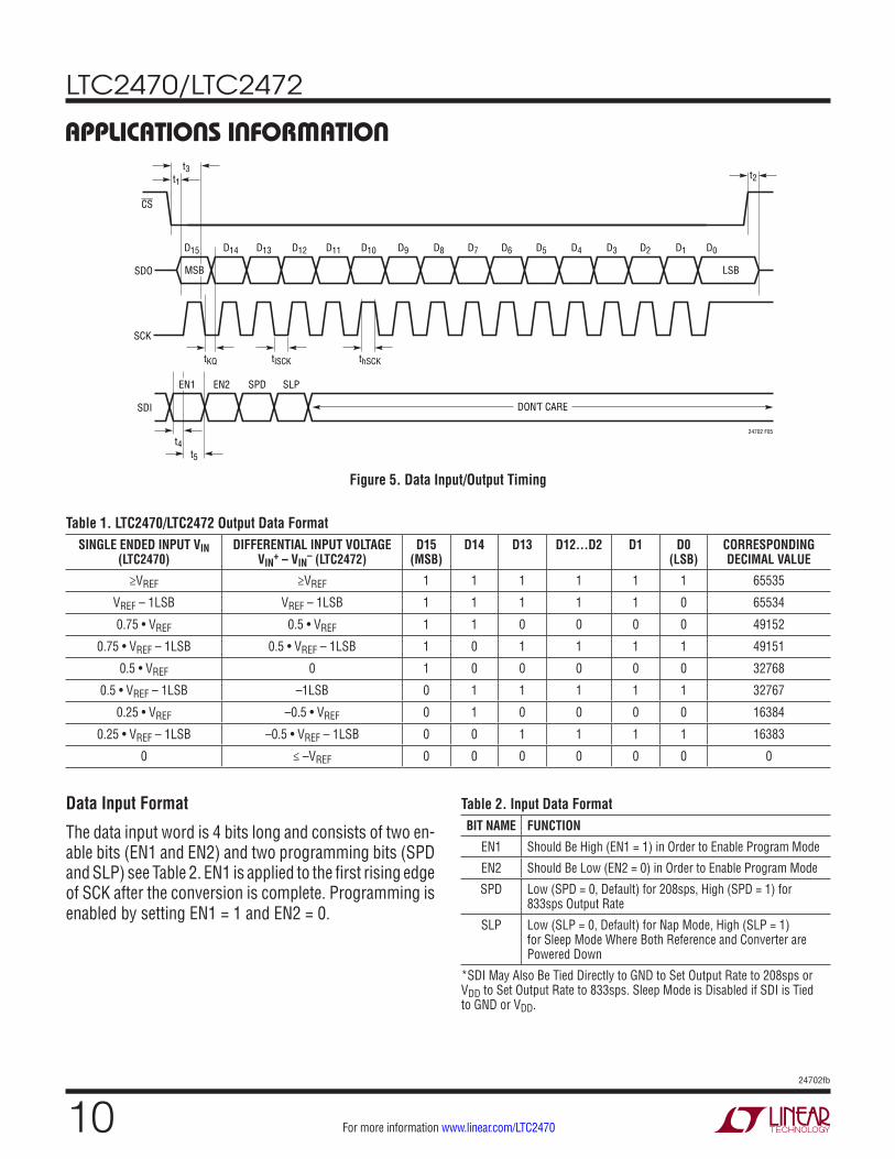
Output Data Format
The LTC2470/LTC2472 generates a 16-bit direct binary encoded result. It is provided as a 16-bit serial stream through the SDO output pin under the control of the SCK input pin (see Figure 5).
The LTC2472 (differential input) output code is given by 32768 • (VIN
+ – VIN–)/VREF + 32768. The first bit output
by the LTC2472, D15, is the MSB, which is 1 for VIN+ ≥
VIN– and 0 for VIN
+ < VIN–. This bit is followed by succes-
sively less significant bits (D14, D13, …) until the LSB is output by the LTC2472, see Table 1.
The LTC2470 (single-ended input) output code is a direct binary encoded result, see Table 1.
During the data output operation the CS input pin must be pulled low (CS = LOW). The data output process starts with the most significant bit of the result being present at the SDO output pin (SDO = D15) once CS goes low. A new data bit appears at the SDO output pin after each falling edge detected at the SCK input pin. The output data can be reliably latched on the rising edge of SCK.
applicaTions inForMaTion
LTC2470/LTC2472
1024702fb
For more information www.linear.com/LTC2470
applicaTions inForMaTion
Data Input Format
The data input word is 4 bits long and consists of two en-able bits (EN1 and EN2) and two programming bits (SPD and SLP) see Table 2. EN1 is applied to the first rising edge of SCK after the conversion is complete. Programming is enabled by setting EN1 = 1 and EN2 = 0.
Table 2. Input Data FormatBIT NAME FUNCTION
EN1 Should Be High (EN1 = 1) in Order to Enable Program Mode
EN2 Should Be Low (EN2 = 0) in Order to Enable Program Mode
SPD Low (SPD = 0, Default) for 208sps, High (SPD = 1) for 833sps Output Rate
SLP Low (SLP = 0, Default) for Nap Mode, High (SLP = 1) for Sleep Mode Where Both Reference and Converter are Powered Down
*SDI May Also Be Tied Directly to GND to Set Output Rate to 208sps or VDD to Set Output Rate to 833sps. Sleep Mode is Disabled if SDI is Tied to GND or VDD.
Table 1. LTC2470/LTC2472 Output Data FormatSINGLE ENDED INPUT VIN
(LTC2470)DIFFERENTIAL INPUT VOLTAGE
VIN+ – VIN
– (LTC2472)D15
(MSB)D14 D13 D12...D2 D1 D0
(LSB)CORRESPONDING DECIMAL VALUE
≥VREF ≥VREF 1 1 1 1 1 1 65535
VREF – 1LSB VREF – 1LSB 1 1 1 1 1 0 65534
0.75 • VREF 0.5 • VREF 1 1 0 0 0 0 49152
0.75 • VREF – 1LSB 0.5 • VREF – 1LSB 1 0 1 1 1 1 49151
0.5 • VREF 0 1 0 0 0 0 0 32768
0.5 • VREF – 1LSB –1LSB 0 1 1 1 1 1 32767
0.25 • VREF –0.5 • VREF 0 1 0 0 0 0 16384
0.25 • VREF – 1LSB –0.5 • VREF – 1LSB 0 0 1 1 1 1 16383
0 ≤ –VREF 0 0 0 0 0 0 0
D15
LSBSDO
SCK
D14 D13 D12 D11 D10 D9 D8 D7 D6 D5 D4 D3 D2 D0D1
24702 F05
t1t3
tKQ tlSCK thSCK
t2
CS
MSB
SDI
EN2 SPD SLP
DON’T CARE
t4t5
EN1
Figure 5. Data Input/Output Timing
LTC2470/LTC2472
1124702fb
For more information www.linear.com/LTC2470
applicaTions inForMaTionThe speed bit (SPD) determines the output rate, SPD = 0 (default) for a 208sps and SPD = 1 for a 833sps output rate. The sleep bit (SLP) is used to power down the on-chip reference. In the default mode, the reference re-mains powered up at the conclusion of each conversion cycle while the ADC is automatically powered down at the end of each conversion cycle. If the SLP bit is set HIGH, the reference and the ADC are powered down once the next conversion cycle is completed. The reference and ADC are powered up again once CS is pulled low. The following conversion is invalid if the next conversion is started before the reference has started up (see Figure 3 for reference startup times as a function of compensation capacitor and reference capacitor).
If the sleep mode is not required, SPD can be tied to GND or VDD in order to simplify the user interface. It should be noted that by tying SDI to GND, the output rate will be set to 208sps. Tying SDI to VDD will result in a 833sps output rate.
SERIAL INTERFACE
The LTC2470/LTC2472 transmit the conversion result and receive the start of conversion command through a synchronous 2-, 3- or 4-wire interface. This interface can be used during the DATA OUTPUT state to read the conversion result, program sleep and speed mode, and to trigger a new conversion.
Serial Interface Operation Modes
The modes of operation can be summarized as follows:
1) The LTC2470/LTC2472 function with SCK idle high (commonly known as CPOL = 1) or idle low (commonly known as CPOL = 0).
2) After the 16th bit is read, a new conversion is started if CS is pulled high or SCK is pulled low.
3) At any time during the Data Output state, pulling CS high causes the part to leave the I/O state, abort the output and begin a new conversion.
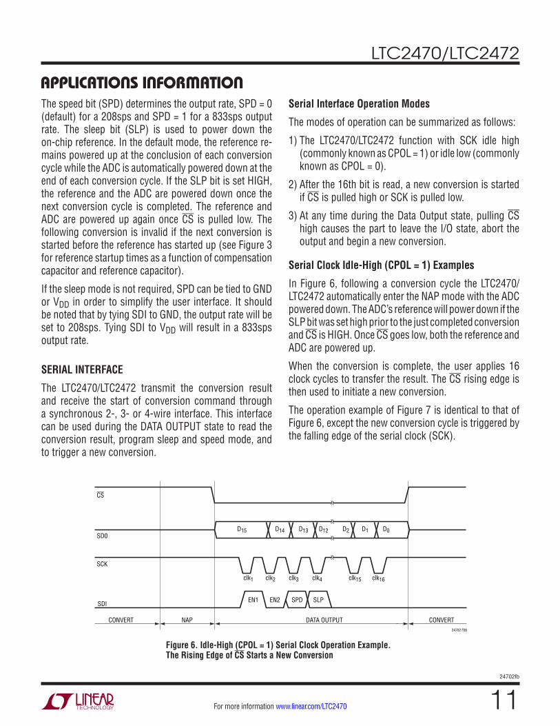
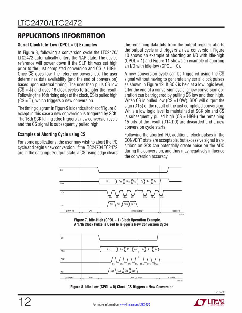
Serial Clock Idle-High (CPOL = 1) Examples
In Figure 6, following a conversion cycle the LTC2470/LTC2472 automatically enter the NAP mode with the ADC powered down. The ADC’s reference will power down if the SLP bit was set high prior to the just completed conversion and CS is HIGH. Once CS goes low, both the reference and ADC are powered up.
When the conversion is complete, the user applies 16 clock cycles to transfer the result. The CS rising edge is then used to initiate a new conversion.
The operation example of Figure 7 is identical to that of Figure 6, except the new conversion cycle is triggered by the falling edge of the serial clock (SCK).
Figure 6. Idle-High (CPOL = 1) Serial Clock Operation Example. The Rising Edge of CS Starts a New Conversion
D15
clk1 clk2 clk3 clk4 clk15 clk16
D14 D13 D12 D2 D1 D0SD0
SCK
CONVERT CONVERTNAP DATA OUTPUT24702 F06
CS
SDI EN2 SPD SLPEN1
LTC2470/LTC2472
1224702fb
For more information www.linear.com/LTC2470
Serial Clock Idle-Low (CPOL = 0) Examples
In Figure 8, following a conversion cycle the LTC2470/LTC2472 automatically enters the NAP state. The device reference will power down if the SLP bit was set high prior to the just completed conversion and CS is HIGH. Once CS goes low, the reference powers up. The user determines data availability (and the end of conversion) based upon external timing. The user then pulls CS low (CS = ↓) and uses 16 clock cycles to transfer the result. Following the 16th rising edge of the clock, CS is pulled high (CS = ↑), which triggers a new conversion.
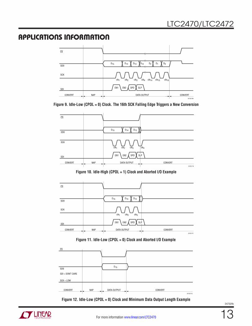
The timing diagram in Figure 9 is identical to that of Figure 8, except in this case a new conversion is triggered by SCK. The 16th SCK falling edge triggers a new conversion cycle and the CS signal is subsequently pulled high.
Examples of Aborting Cycle using CS
For some applications, the user may wish to abort the I/O cycle and begin a new conversion. If the LTC2470/LTC2472 are in the data input/output state, a CS rising edge clears
the remaining data bits from the output register, aborts the output cycle and triggers a new conversion. Figure 10 shows an example of aborting an I/O with idle-high (CPOL = 1) and Figure 11 shows an example of aborting an I/O with idle-low (CPOL = 0).
A new conversion cycle can be triggered using the CS signal without having to generate any serial clock pulses as shown in Figure 12. If SCK is held at a low logic level, after the end of a conversion cycle, a new conversion op-eration can be triggered by pulling CS low and then high. When CS is pulled low (CS = LOW), SDO will output the sign (D15) of the result of the just completed conversion. While a low logic level is maintained at SCK pin and CS is subsequently pulled high (CS = HIGH) the remaining 15 bits of the result (D14:D0) are discarded and a new conversion cycle starts.
Following the aborted I/O, additional clock pulses in the CONVERT state are acceptable, but excessive signal tran-sitions on SCK can potentially create noise on the ADC during the conversion, and thus may negatively influence the conversion accuracy.
applicaTions inForMaTion
Figure 8. Idle-Low (CPOL = 0) Clock. CS Triggers a New Conversion
D15 D14 D13 D12 D2 D1 D0
clk1 clk2 clk3 clk4 clk14 clk15 clk16
SCK
SD0
CONVERT CONVERTNAP DATA OUTPUT24702 F08
CS
SDI EN2 SPD SLPEN1
Figure 7. Idle-High (CPOL = 1) Clock Operation Example. A 17th Clock Pulse is Used to Trigger a New Conversion Cycle
D15 D14 D13 D12 D2 D1 D0SD0
clk1 clk2 clk3 clk4 clk15 clk16 clk17
SCK
CONVERT CONVERTNAP DATA OUTPUT24702 F07
CS
SDI EN2 SPD SLPEN1
LTC2470/LTC2472
1324702fb
For more information www.linear.com/LTC2470
applicaTions inForMaTion
Figure 11. Idle-Low (CPOL = 0) Clock and Aborted I/O Example
Figure 12. Idle-Low (CPOL = 0) Clock and Minimum Data Output Length Example
Figure 10. Idle-High (CPOL = 1) Clock and Aborted I/O Example
D15 D14 D13
clk1 clk2 clk4clk3
CONVERT CONVERTNAP DATA OUTPUT24702 F10
SD0
SCK
CS
SDI EN2 SPDEN1 SLP
D15 D14 D13SD0
clk1 clk2 clk3
SCK
CONVERT CONVERTNAP DATA OUTPUT24702 F11
CS
SDI EN2 SPDEN1 SLP
SCK = LOW
SD0
CONVERT CONVERTNAP DATA OUTPUT24702 F12
D15
CS
SDI = DON’T CARE
Figure 9. Idle-Low (CPOL = 0) Clock. The 16th SCK Falling Edge Triggers a New Conversion
D15 D14 D13 D12 D2 D1 D0SD0
clk1 clk2 clk3 clk4 clk15clk14 clk16
SCK
CONVERT CONVERTNAP DATA OUTPUT24702 F09
CS
SDI EN2 SPD SLPEN1
LTC2470/LTC2472
1424702fb
For more information www.linear.com/LTC2470
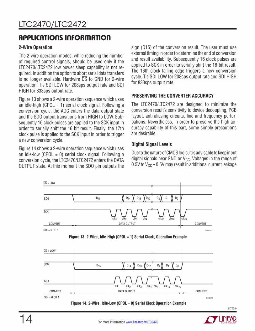
applicaTions inForMaTion2-Wire Operation
The 2-wire operation modes, while reducing the number of required control signals, should be used only if the LTC2470/LTC2472 low power sleep capability is not re-quired. In addition the option to abort serial data transfers is no longer available. Hardwire CS to GND for 2-wire operation. Tie SDI LOW for 208sps output rate and SDI HIGH for 833sps output rate.
Figure 13 shows a 2-wire operation sequence which uses an idle-high (CPOL = 1) serial clock signal. Following a conversion cycle, the ADC enters the data output state and the SDO output transitions from HIGH to LOW. Sub-sequently 16 clock pulses are applied to the SCK input in order to serially shift the 16 bit result. Finally, the 17th clock pulse is applied to the SCK input in order to trigger a new conversion cycle.
Figure 14 shows a 2-wire operation sequence which uses an idle-low (CPOL = 0) serial clock signal. Following a conversion cycle, the LTC2470/LTC2472 enters the DATA OUTPUT state. At this moment the SDO pin outputs the
sign (D15) of the conversion result. The user must use external timing in order to determine the end of conversion and result availability. Subsequently 16 clock pulses are applied to SCK in order to serially shift the 16-bit result. The 16th clock falling edge triggers a new conversion cycle. Tie SDI LOW for 208sps output rate and SDI HIGH for 833sps output rate.
PRESERVING THE CONVERTER ACCURACY
The LTC2470/LTC2472 are designed to minimize the conversion result’s sensitivity to device decoupling, PCB layout, anti-aliasing circuits, line and frequency pertur-bations. Nevertheless, in order to preserve the high ac-curacy capability of this part, some simple precautions are desirable.
Digital Signal Levels
Due to the nature of CMOS logic, it is advisable to keep input digital signals near GND or VCC. Voltages in the range of 0.5V to VCC – 0.5V may result in additional current leakage
Figure 13. 2-Wire, Idle-High (CPOL = 1) Serial Clock, Operation Example
Figure 14. 2-Wire, Idle-Low (CPOL = 0) Serial Clock Operation Example
D15 D14 D13 D12 D2 D1 D0SD0
clk1 clk2 clk3 clk4 clk15 clk16 clk17
SCK
CONVERT
SDI = 0 OR 1
CONVERTDATA OUTPUT
CS = LOW
24702 F13
D15 D14 D13 D12 D2 D1 D0SD0
CS = LOW
clk1 clk2 clk3 clk14clk4 clk15 clk16
SCK
CONVERT CONVERTDATA OUTPUT
SDI = 0 OR 1 24702 F14
LTC2470/LTC2472
1524702fb
For more information www.linear.com/LTC2470
applicaTions inForMaTionfrom the part. Undershoot and overshoot should also be minimized, particularly while the chip is converting. It is thus beneficial to keep edge rates of about 10ns and limit overshoot and undershoot to less than 0.3V.
Noisy external circuitry can potentially impact the output under 2-wire operation. In particular, it is possible to get the LTC2470/LTC2472 into an unknown state if an SCK pulse is missed or noise triggers an extra SCK pulse. In this situation, it is impossible to distinguish SDO = 1 (in-dicating conversion in progress) from valid “1” data bits. A method to prevent this from happening is to read 32 bits each cycle instead of 16 and ignoring the last 16 data bits. In the case where a noisy bus leads to an unknown SCK clock count, the extra 16 SCK clock pulses will force a new conversion and place the device in a known state.
Driving VCC and GND
In relation to the VCC and GND pins, the LTC2470/LTC2472 combines internal high frequency decoupling with damping elements, which reduce the ADC performance sensitivity to PCB layout and external components. Nevertheless, the very high accuracy of this converter is best pre-served by careful low and high frequency power supply decoupling.
A 0.1µF, high quality, ceramic capacitor in parallel with a 10µF low ESR ceramic capacitor should be connected between the VCC and GND pins, as close as possible to the package. The 0.1µF capacitor should be placed closest to the ADC package. It is also desirable to avoid any via in the circuit path, starting from the converter VCC pin, passing through these two decoupling capacitors, and returning to the converter GND pin. The area encompassed by this circuit path, as well as the path length, should be minimized.
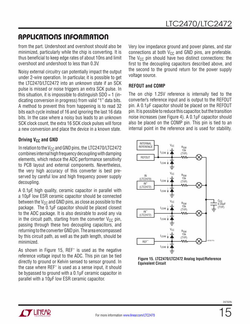
As shown in Figure 15, REF– is used as the negative reference voltage input to the ADC. This pin can be tied directly to ground or Kelvin sensed to sensor ground. In the case where REF– is used as a sense input, it should be bypassed to ground with a 0.1μF ceramic capacitor in parallel with a 10μF low ESR ceramic capacitor.
Very low impedance ground and power planes, and star connections at both VCC and GND pins, are preferable. The VCC pin should have two distinct connections: the first to the decoupling capacitors described above, and the second to the ground return for the power supply voltage source.
REFOUT and COMP
The on chip 1.25V reference is internally tied to the converter’s reference input and is output to the REFOUT pin. A 0.1μF capacitor should be placed on the REFOUT pin. It is possible to reduce this capacitor, but the transition noise increases (see Figure 4). A 0.1μF capacitor should also be placed on the COMP pin. This pin is tied to an internal point in the reference and is used for stability.
Figure 15. LTC2470/LTC2472 Analog Input/Reference Equivalent Circuit
RSW15k
(TYP)ILEAK
ILEAK
VCC
VCC
VCC
VCC
CEQ0.35pF(TYP)
IN+
(LTC2472)
IN–
(LTC2472)
IN(LTC2470)
REF–
REFOUT
INTERNALREFERENCE
24702 F15
RSW15k
(TYP)ILEAK
ILEAK
RSW15k
(TYP)
ILEAK
ILEAK
RSW15k
(TYP)
ILEAK
ILEAK
LTC2470/LTC2472
1624702fb
For more information www.linear.com/LTC2470
applicaTions inForMaTionIn order for the reference to remain stable, the capacitor placed on the COMP pin must be greater than or equal to the capacitor tied to the REFOUT pin. The REFOUT pin cannot be overridden by an external voltage.
Depending on the size of the capacitors tied to the REFOUT and COMP pins, the internal reference has a corresponding start up time. This start up time is typically 12ms when 0.1μF capacitors are used. The first conversion following power up can be discarded using the data abort com-mand or simply read and ignored. Depending on the value chosen for CCOMP and CREFOUT, the reference startup can take more than one conversion period, see Figure 3. If the startup time is less than 1.2ms (833sps output rate) or 4.8ms (208sps output rate) then conversions following the first period are accurate to the device specifications. If the startup time exceeds 1.2ms or 4.8ms then the user can wait the appropriate time or use the fixed conversion period as a startup timer by ignoring results within the unsettled period. Once the reference has settled all sub-sequent conversion results are valid. If the user places the device into the sleep mode (SLP = 1, reference powered down) the reference will require a startup time proportional to the value of CCOMP and CREFOUT, see Figure 3.
If the reference is put to sleep (program SLP = 1 and CS = 1) the reference is powered down after the next conversion. This last conversion result is valid. On CS falling edge, the reference is powered back up. In order to ensure the reference output has settled before the next conversion, the power up time can be extended by delaying the data read after the falling edge of CS. Once all 16 bits are read from the device or CS is brought HIGH, the next conver-sion automatically begins. In the default operation, the reference remains powered up at the conclusion of the conversion cycle.
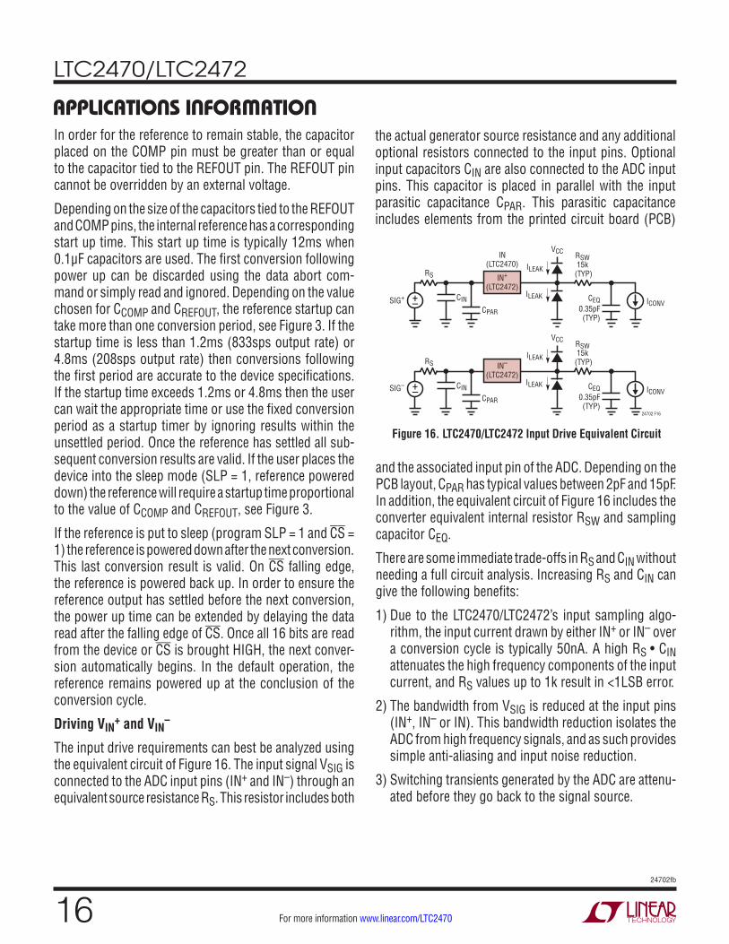
Driving VIN+ and VIN
–
The input drive requirements can best be analyzed using the equivalent circuit of Figure 16. The input signal VSIG is connected to the ADC input pins (IN+ and IN–) through an equivalent source resistance RS. This resistor includes both
the actual generator source resistance and any additional optional resistors connected to the input pins. Optional input capacitors CIN are also connected to the ADC input pins. This capacitor is placed in parallel with the input parasitic capacitance CPAR. This parasitic capacitance includes elements from the printed circuit board (PCB)
Figure 16. LTC2470/LTC2472 Input Drive Equivalent Circuit
ILEAK
ILEAK
RSW15k
(TYP)
ICONVCIN
IN+
(LTC2472)
IN(LTC2470)
VCC
SIG+
SIG–
RS
CEQ0.35pF(TYP)
CPAR
+–
24702 F16
ILEAK
ILEAK
RSW15k
(TYP)
ICONVCIN
IN–
(LTC2472)
VCC
RS
CEQ0.35pF(TYP)
CPAR
+–
and the associated input pin of the ADC. Depending on the PCB layout, CPAR has typical values between 2pF and 15pF. In addition, the equivalent circuit of Figure 16 includes the converter equivalent internal resistor RSW and sampling capacitor CEQ.
There are some immediate trade-offs in RS and CIN without needing a full circuit analysis. Increasing RS and CIN can give the following benefits:
1) Due to the LTC2470/LTC2472’s input sampling algo-rithm, the input current drawn by either IN+ or IN– over a conversion cycle is typically 50nA. A high RS • CIN attenuates the high frequency components of the input current, and RS values up to 1k result in <1LSB error.
2) The bandwidth from VSIG is reduced at the input pins (IN+, IN– or IN). This bandwidth reduction isolates the ADC from high frequency signals, and as such provides simple anti-aliasing and input noise reduction.
3) Switching transients generated by the ADC are attenu-ated before they go back to the signal source.
LTC2470/LTC2472
1724702fb
For more information www.linear.com/LTC2470
applicaTions inForMaTion4) A large CIN gives a better AC ground at the input pins,
helping reduce reflections back to the signal source.
5) Increasing RS protects the ADC by limiting the current during an outside-the-rails fault condition.
There is a limit to how large RS • CIN should be for a given application. Increasing RS beyond a given point increases the voltage drop across RS due to the input current, to the point that significant measurement errors exist. Additionally, for some applications, increasing the RS • CIN product too much may unacceptably attenuate the signal at frequencies of interest.
For most applications, it is desirable to implement CIN as a high-quality 0.1µF ceramic capacitor and to set RS ≤ 1k. This capacitor should be located as close as possible to the actual IN+, IN– and IN package pins. Furthermore, the area encompassed by this circuit path, as well as the path length, should be minimized.
In the case of a 2-wire sensor that is not remotely grounded, it is desirable to split RS and place series resistors in the ADC input line as well as in the sensor ground return line, which should be tied to the ADC GND pin using a star connection topology.
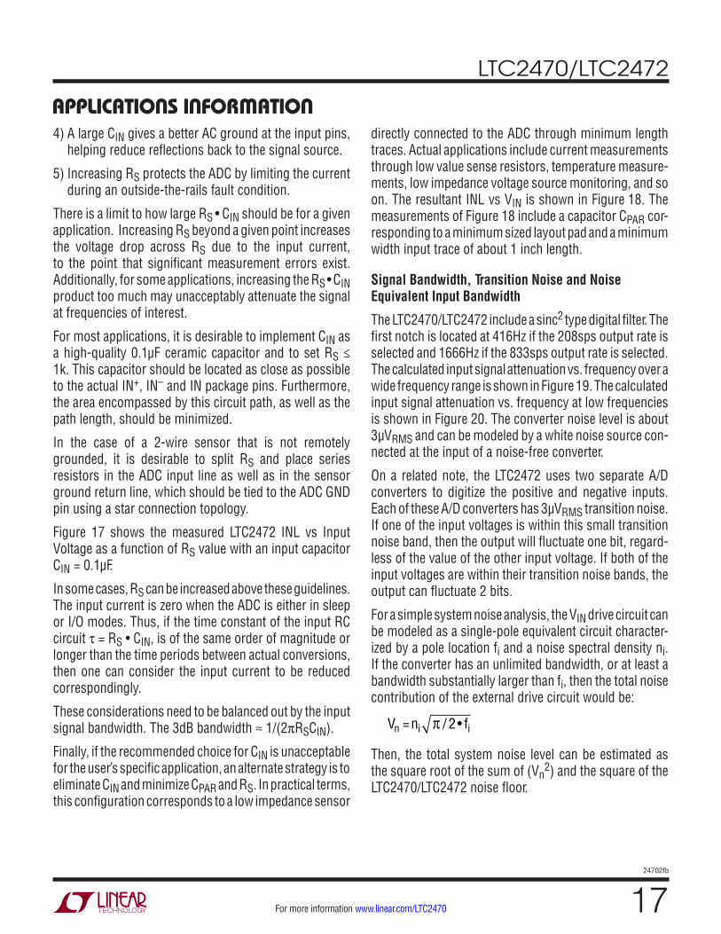
Figure 17 shows the measured LTC2472 INL vs Input Voltage as a function of RS value with an input capacitor CIN = 0.1µF.
In some cases, RS can be increased above these guidelines. The input current is zero when the ADC is either in sleep or I/O modes. Thus, if the time constant of the input RC circuit t = RS • CIN, is of the same order of magnitude or longer than the time periods between actual conversions, then one can consider the input current to be reduced correspondingly.
These considerations need to be balanced out by the input signal bandwidth. The 3dB bandwidth ≈ 1/(2pRSCIN).
Finally, if the recommended choice for CIN is unacceptable for the user’s specific application, an alternate strategy is to eliminate CIN and minimize CPAR and RS. In practical terms, this configuration corresponds to a low impedance sensor
directly connected to the ADC through minimum length traces. Actual applications include current measurements through low value sense resistors, temperature measure-ments, low impedance voltage source monitoring, and so on. The resultant INL vs VIN is shown in Figure 18. The measurements of Figure 18 include a capacitor CPAR cor-responding to a minimum sized layout pad and a minimum width input trace of about 1 inch length.
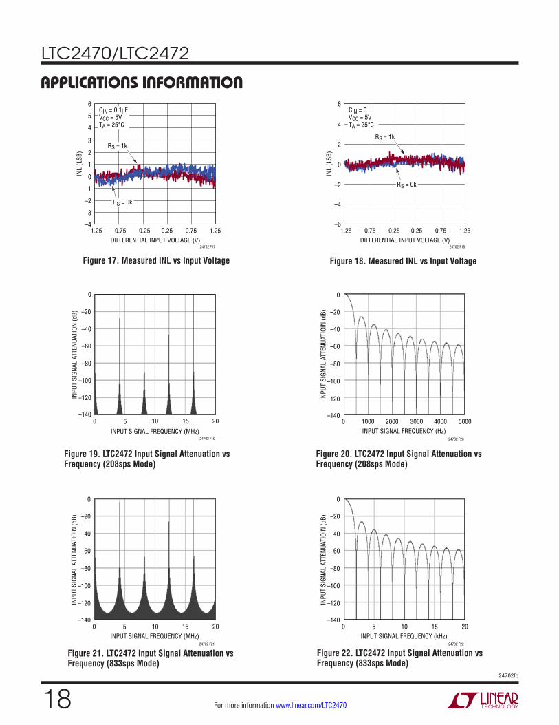
Signal Bandwidth, Transition Noise and Noise Equivalent Input Bandwidth
The LTC2470/LTC2472 include a sinc2 type digital filter. The first notch is located at 416Hz if the 208sps output rate is selected and 1666Hz if the 833sps output rate is selected. The calculated input signal attenuation vs. frequency over a wide frequency range is shown in Figure 19. The calculated input signal attenuation vs. frequency at low frequencies is shown in Figure 20. The converter noise level is about 3µVRMS and can be modeled by a white noise source con-nected at the input of a noise-free converter.
On a related note, the LTC2472 uses two separate A/D converters to digitize the positive and negative inputs. Each of these A/D converters has 3µVRMS transition noise. If one of the input voltages is within this small transition noise band, then the output will fluctuate one bit, regard-less of the value of the other input voltage. If both of the input voltages are within their transition noise bands, the output can fluctuate 2 bits.
For a simple system noise analysis, the VIN drive circuit can be modeled as a single-pole equivalent circuit character-ized by a pole location fi and a noise spectral density ni. If the converter has an unlimited bandwidth, or at least a bandwidth substantially larger than fi, then the total noise contribution of the external drive circuit would be:
Vn =ni π / 2• fi
Then, the total system noise level can be estimated as the square root of the sum of (Vn
2) and the square of the LTC2470/LTC2472 noise floor.
LTC2470/LTC2472
1824702fb
For more information www.linear.com/LTC2470
Figure 19. LTC2472 Input Signal Attenuation vs Frequency (208sps Mode)
Figure 20. LTC2472 Input Signal Attenuation vs Frequency (208sps Mode)
applicaTions inForMaTion
Figure 17. Measured INL vs Input Voltage Figure 18. Measured INL vs Input Voltage
Figure 21. LTC2472 Input Signal Attenuation vs Frequency (833sps Mode)
Figure 22. LTC2472 Input Signal Attenuation vs Frequency (833sps Mode)
DIFFERENTIAL INPUT VOLTAGE (V)–1.25 –0.75 –0.25
INL
(LSB
) 2
3
6
24702 F17
–1
0
1
5
4
–3
–2
–40.25 0.75 1.25
CIN = 0.1µFVCC = 5VTA = 25°C
RS = 1k
RS = 0k
DIFFERENTIAL INPUT VOLTAGE (V)–1.25 –0.75 –0.25
INL
(LSB
)
2
6
24702 F18
–2
0
4
–6
–4
0.25 0.75 1.25
CIN = 0VCC = 5VTA = 25°C
RS = 1k
RS = 0k
INPUT SIGNAL FREQUENCY (MHz)
0
INPU
T SI
GNAL
ATT
ENUA
TION
(dB)
–40
0
20
24702 F19
–60
–80
–20
–140
–120
–100
5 10 15INPUT SIGNAL FREQUENCY (Hz)
0
INPU
T SI
GNAL
ATT
ENUA
TIOI
N (d
B)
–80
–40
0
4000
24702 F20
–120
–100
–60
–20
–1401000 2000 3000 5000
INPUT SIGNAL FREQUENCY (MHz)0
INPU
T SI
GNAL
ATT
ENUA
TIOI
N (d
B)
–80
–40
0
20
24702 F21
–120
–100
–60
–20
–1405 10 15
INPUT SIGNAL FREQUENCY (kHz)0
INPU
T SI
GNAL
ATT
ENUA
TIOI
N (d
B)
–80
–40
0
20
24702 F22
–120
–100
–60
–20
–1405 10 15
LTC2470/LTC2472
1924702fb
For more information www.linear.com/LTC2470
package DescripTion
3.00 ±0.10(4 SIDES)
NOTE:1. DRAWING IS NOT A JEDEC PACKAGE OUTLINE2. DRAWING NOT TO SCALE3. ALL DIMENSIONS ARE IN MILLIMETERS4. DIMENSIONS OF EXPOSED PAD ON BOTTOM OF PACKAGE DO NOT INCLUDE MOLD FLASH. MOLD FLASH, IF PRESENT, SHALL NOT EXCEED 0.15mm ON ANY SIDE5. EXPOSED PAD AND TIE BARS SHALL BE SOLDER PLATED6. SHADED AREA IS ONLY A REFERENCE FOR PIN 1 LOCATION ON THE TOP AND BOTTOM OF PACKAGE
0.40 ±0.10
BOTTOM VIEW—EXPOSED PAD
1.65 ±0.10
0.75 ±0.05
R = 0.115TYP
16
127
PIN 1TOP MARK
(SEE NOTE 6)
0.200 REF
0.00 – 0.05
(DD12) DFN 0106 REV A
RECOMMENDED SOLDER PAD PITCH AND DIMENSIONSAPPLY SOLDER MASK TO AREAS THAT ARE NOT SOLDERED
0.23 ±0.05
0.25 ±0.05
2.25 REF
2.38 ±0.051.65 ±0.052.10 ±0.05
0.70 ±0.05
3.50 ±0.05
PACKAGEOUTLINE
PIN 1 NOTCHR = 0.20 OR0.25 × 45°CHAMFER
2.38 ±0.10
2.25 REF0.45 BSC
0.45 BSC
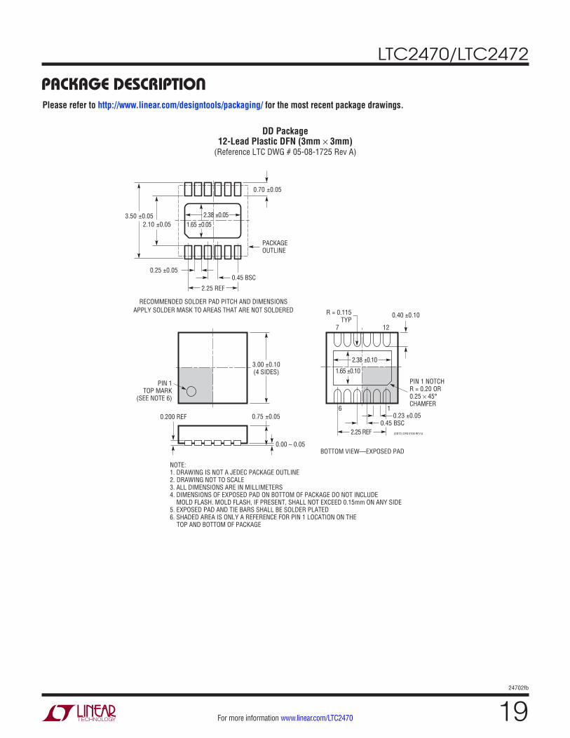
DD Package12-Lead Plastic DFN (3mm × 3mm)
(Reference LTC DWG # 05-08-1725 Rev A)
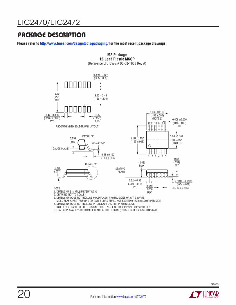
Please refer to http://www.linear.com/designtools/packaging/ for the most recent package drawings.
LTC2470/LTC2472
2024702fb
For more information www.linear.com/LTC2470
package DescripTion
MSOP (MS12) 0213 REV A
0.53 ±0.152(.021 ±.006)
SEATINGPLANE
0.18(.007)
1.10(.043)MAX
0.22 – 0.38(.009 – .015)
TYP
0.86(.034)REF
0.650(.0256)
BSC
12 11 10 9 8 7
NOTE:1. DIMENSIONS IN MILLIMETER/(INCH)2. DRAWING NOT TO SCALE3. DIMENSION DOES NOT INCLUDE MOLD FLASH, PROTRUSIONS OR GATE BURRS. MOLD FLASH, PROTRUSIONS OR GATE BURRS SHALL NOT EXCEED 0.152mm (.006") PER SIDE4. DIMENSION DOES NOT INCLUDE INTERLEAD FLASH OR PROTRUSIONS. INTERLEAD FLASH OR PROTRUSIONS SHALL NOT EXCEED 0.152mm (.006") PER SIDE5. LEAD COPLANARITY (BOTTOM OF LEADS AFTER FORMING) SHALL BE 0.102mm (.004") MAX
0.254(.010) 0° – 6° TYP
DETAIL “A”
DETAIL “A”
GAUGE PLANE
5.10(.201)MIN
3.20 – 3.45(.126 – .136)
0.889 ±0.127(.035 ±.005)
RECOMMENDED SOLDER PAD LAYOUT
0.42 ±0.038(.0165 ±.0015)
TYP
0.65(.0256)
BSC
4.039 ±0.102(.159 ±.004)
(NOTE 3)
0.1016 ±0.0508(.004 ±.002)
1 2 3 4 5 6
3.00 ±0.102(.118 ±.004)
(NOTE 4)
0.406 ±0.076(.016 ±.003)
REF
4.90 ±0.152(.193 ±.006)
MS Package12-Lead Plastic MSOP
(Reference LTC DWG # 05-08-1668 Rev A)
Please refer to http://www.linear.com/designtools/packaging/ for the most recent package drawings.
LTC2470/LTC2472
2124702fb
For more information www.linear.com/LTC2470
Information furnished by Linear Technology Corporation is believed to be accurate and reliable. However, no responsibility is assumed for its use. Linear Technology Corporation makes no representa-tion that the interconnection of its circuits as described herein will not infringe on existing patent rights.
revision hisToryREV DATE DESCRIPTION PAGE NUMBER
A 9/13 Clarified maximum operating output rate as 208sps/833sps Global
B 1/14 Removed No Missing Codes Resolution 1, 3
LTC2470/LTC2472
2224702fb
For more information www.linear.com/LTC2470Linear Technology Corporation1630 McCarthy Blvd., Milpitas, CA 95035-7417
LINEAR TECHNOLOGY CORPORATION 2009
LT 0114 REV B • PRINTED IN USA
(408) 432-1900 ● FAX: (408) 434-0507 ● www.linear.com/LTC2470
relaTeD parTsPART NUMBER DESCRIPTION COMMENTS
LTC1860/LTC1861 12-Bit, 5V, 1-/2-Channel 250ksps SAR ADC in MSOP 850µA at 250ksps, 2µA at 1ksps, SO-8 and MSOP Packages
LTC1860L/LTC1861L 12-Bit, 3V, 1-/2-Channel 150ksps SAR ADC 450µA at 150ksps, 10µA at 1ksps, SO-8 and MSOP Packages
LTC1864/LTC1865 16-Bit, 5V, 1-/2-Channel 250ksps SAR ADC in MSOP 850µA at 250ksps, 2µA at 1ksps, SO-8 and MSOP Packages
LTC1864L/LTC1865L 16-bit, 3V, 1-/2-Channel 150ksps SAR ADC 450µA at 150ksps, 10µA at 1ksps, SO-8 and MSOP Packages
LTC2360 12-Bit, 100ksps SAR ADC 3V Supply, 1.5mW at 100ksps, TSOT 6-pin/8-pin Packages
LTC2440 24-Bit No Latency ∆∑™ ADC 200nVRMS Noise, 4kHz Output Rate, 15ppm INL
LTC2480 16-Bit, Differential Input, No Latency ∆∑ ADC, with PGA, Temp. Sensor, SPI
Easy-Drive Input Current Cancellation, 600nVRMS Noise, Tiny 10-Lead DFN Package
LTC2481 16-Bit, Differential Input, No Latency ∆∑ ADC, with PGA, Temp. Sensor, I2C
Easy-Drive Input Current Cancellation, 600nVRMS Noise, Tiny 10-Lead DFN Package
LTC2482 16-Bit, Differential Input, No Latency ∆∑ ADC, SPI Easy-Drive Input Current Cancellation, 600nVRMS Noise, Tiny 10-Lead DFN Package
LTC2483 16-Bit, Differential Input, No Latency ∆∑ ADC, I2C Easy-Drive Input Current Cancellation, 600nVRMS Noise, Tiny 10-Lead DFN Package
LTC2484 24-Bit, Differential Input, No Latency ∆∑ ADC, SPI with Temp. Sensor
Easy-Drive Input Current Cancellation, 600nVRMS Noise, Tiny 10-Lead DFN Package
LTC2485 24-Bit, Differential Input, No Latency ∆∑ ADC, I2C with Temp. Sensor
Easy-Drive Input Current Cancellation, 600nVRMS Noise, Tiny 10-Lead DFN Package
LTC6241 Dual, 18MHz, Low Noise, Rail-to-Rail Op Amp 550nVP-P Noise, 125µV Offset Max
LTC2450 Easy-to-Use, Ultra-Tiny 16-Bit ADC, SPI, 0V to 5.5V Input Range
2 LSB INL, 50nA Sleep current, Tiny 2mm × 2mm DFN-6 Package, 30Hz Output Rate
LTC2450-1 Easy-to-Use, Ultra-Tiny 16-Bit ADC, SPI, 0V to 5.5V Input Range
2 LSB INL, 50nA Sleep Current, Tiny 2mm × 2mm DFN-6 Package, 60Hz Output Rate
LTC2451 Easy-to-Use, Ultra-Tiny 16-Bit ADC, I2C, 0V to 5.5V Input Range
2 LSB INL, 50nA Sleep Current, Tiny 3mm × 2mm DFN-8 or TSOT Package, Programmable 30Hz/60Hz Output Rates
LTC2452 Easy-to-Use, Ultra-Tiny 16-Bit Differential ADC, SPI, ±5.5V Input Range
2 LSB INL, 50nA Sleep Current, Tiny 3mm × 2mm DFN-8 or TSOT Package
LTC2453 Easy-to-Use, Ultra-Tiny 16-Bit Differential ADC, I2C, ±5.5V Input Range
2 LSB INL, 50nA Sleep Current, Tiny 3mm × 2mm DFN-8 or TSOT Package
LTC2460 Ultra-Tiny 16-Bit ∆∑ ADC with 10ppm Reference Pin and Software Compatible with LTC2470, 60Hz Output Rate
LTC2462 Ultra-Tiny 16-Bit ∆∑ ADC with 10ppm Reference Pin and Software Compatible with LTC2472, 60Hz Output Rate
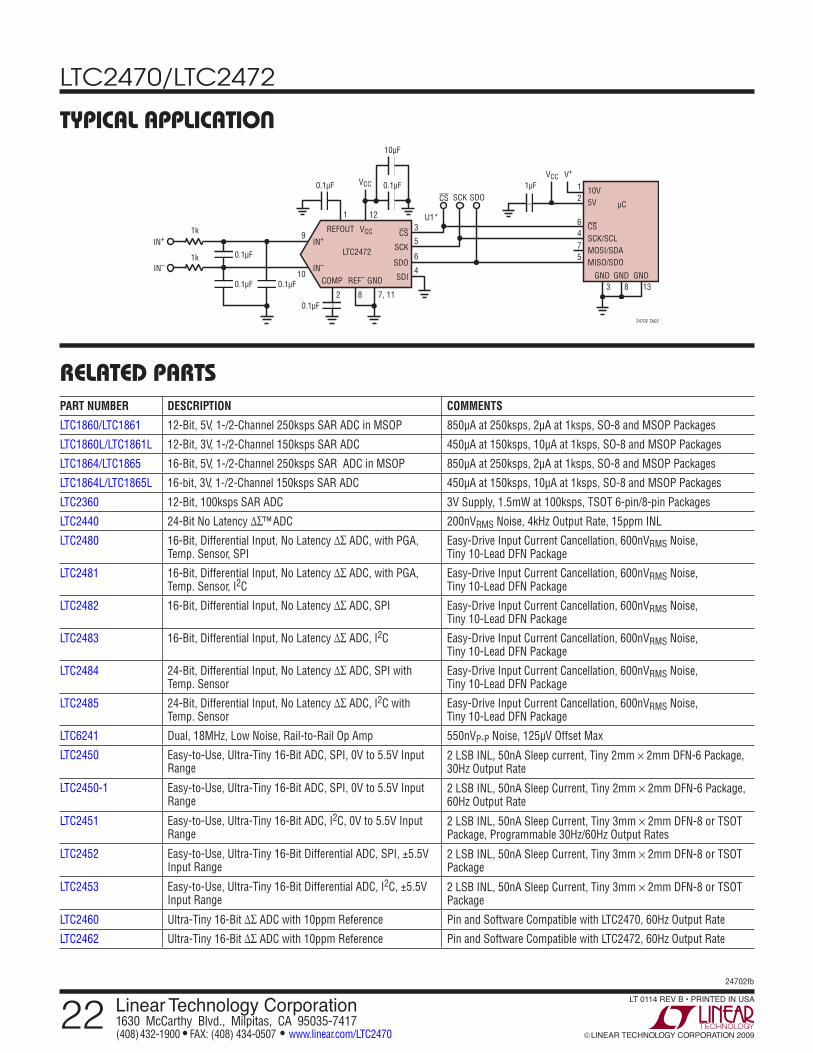
0.1µFVCC
IN+
IN–
24702 TA02
10µF
0.1µF
7, 118
121
0.1µF
0.1µF
0.1µF
1k
1k
10
9
6
5
3
10V5V
CSSCK/SCLMOSI/SDAMISO/SDO
GND GND GND
12
6475
1µFVCC V+
1383
µCCS SCK SDO
U1*
IN+REFOUT
REF–
VCC
GND
2
COMPIN–
LTC2472
CS
SCK
SDO4
SDI
0.1µF
Typical applicaTion