TPA3003D2: 3-W Stereo Class-D Audio Power Amplifier w/DC ...
LM48413
www.ti.com SNAS460B –NOVEMBER 2008–REVISED MARCH 2013
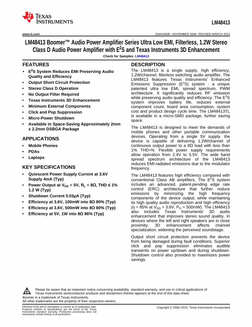
LM48413 Boomer™ Audio Power Amplifier Series Ultra Low EMI, Filterless, 1.2W StereoClass D Audio Power Amplifier with E2S and Texas Instruments 3D Enhancement
Check for Samples: LM48413
1FEATURES DESCRIPTIONThe LM48413 is a single supply, high efficiency,
23• E2S System Reduces EMI Preserving Audio1.2W/channel, filterless switching audio amplifier. TheQuality and EfficiencyLM48413 features Texas Instruments' Enhanced
• Output Short Circuit Protection Emissions Suppression (E2S) system - a unique• Stereo Class D Operation patented ultra low EMI, spread spectrum, PWM
architecture. It significantly reduces RF emission• No Output Filter Requiredwhile preserving audio quality and efficiency. The E2S
• Texas Instruments 3D Enhancement system improves battery life, reduces external• Minimum External Components component count, board area consumption, system
cost and product design cycle time. The LM48413TL• Click and Pop Suppressionis available in a micro-SMD package, further saving• Micro-Power Shutdown space.
• Available in Space-Saving Approximately 2mmThe LM48413 is designed to meet the demands ofx 2.2mm DSBGA Packagemobile phones and other portable communicationdevices. Operating from a single 5V supply, theAPPLICATIONS device is capable of delivering 1.2W/channel ofcontinuous output power to a 8Ω load with less than• Mobile Phones1% THD+N. Flexible power supply requirements• PDAsallow operation from 2.4V to 5.5V. The wide band
• Laptops spread spectrum architecture of the LM48413reduces EMI-radiated emissions due to the modulator
KEY SPECIFICATIONS frequency.• Quiescent Power Supply Current at 3.6V The LM48413 features high efficiency compared with
Supply 4mA (Typ) conventional Class AB amplifiers. The E2S systemincludes an advanced, patent-pending edge rate• Power Output at VDD = 5V, RL = 8Ω, THD ≤ 1%control (ERC) architecture that further reduce1.2 W (Typ)emissions by minimizing the high frequency
• Shutdown Current 0.03µA (Typ) components of the device output, while maintaining• Efficiency at 3.6V, 100mW into 8Ω 80% (Typ) its high quality audio reproduction and high efficiency
(η = 85% at VDD = 3.6V, PO = 500mW). The LM48413• Efficiency at 3.6V, 500mW into 8Ω 80% (Typ)also includes Texas Instruments' 3D audio• Efficiency at 5V, 1W into 8Ω 86% (Typ)enhancement that improves stereo sound quality. Indevices where the left and right speakers are in closeproximity, 3D enhancement affects channelspecialization, widening the perceived soundstage.
Output short circuit protection prevents the devicefrom being damaged during fault conditions. Superiorclick and pop suppression eliminates audibletransients on power up/down and during shutdown.Shutdown control also provided to maximizes powersavings.
1
Please be aware that an important notice concerning availability, standard warranty, and use in critical applications ofTexas Instruments semiconductor products and disclaimers thereto appears at the end of this data sheet.
2Boomer is a trademark of Texas Instruments.3All other trademarks are the property of their respective owners.
PRODUCTION DATA information is current as of publication date. Copyright © 2008–2013, Texas Instruments IncorporatedProducts conform to specifications per the terms of the TexasInstruments standard warranty. Production processing does notnecessarily include testing of all parameters.
LM48413
SNAS460B –NOVEMBER 2008–REVISED MARCH 2013 www.ti.com
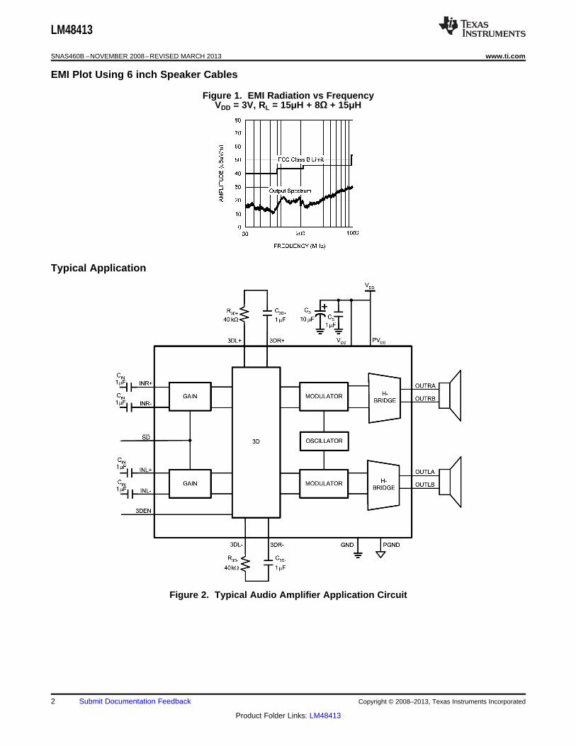
EMI Plot Using 6 inch Speaker Cables
Figure 1. EMI Radiation vs FrequencyVDD = 3V, RL = 15μH + 8Ω + 15μH
Typical Application
Figure 2. Typical Audio Amplifier Application Circuit
2 Submit Documentation Feedback Copyright © 2008–2013, Texas Instruments Incorporated
Product Folder Links: LM48413
LM48413
www.ti.com SNAS460B –NOVEMBER 2008–REVISED MARCH 2013
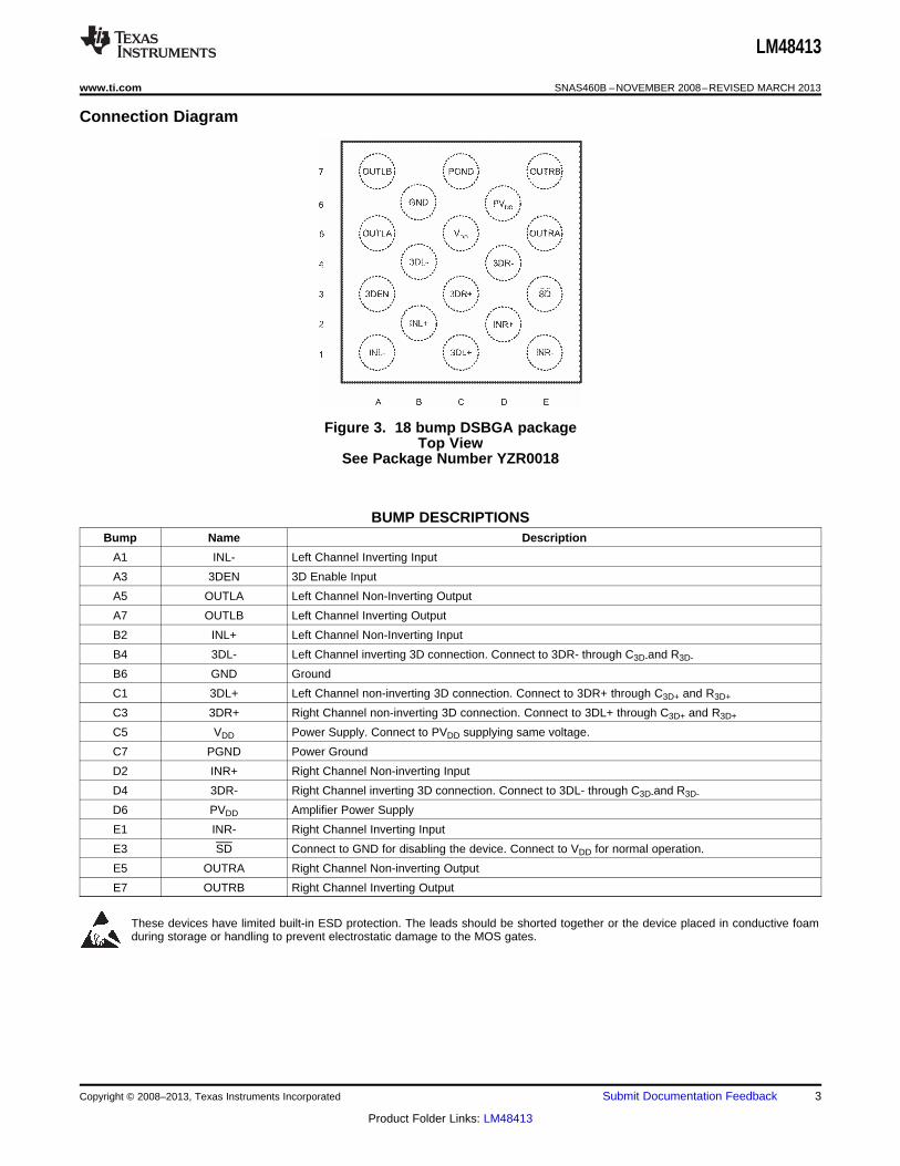
Connection Diagram
Figure 3. 18 bump DSBGA packageTop View
See Package Number YZR0018
BUMP DESCRIPTIONSBump Name Description
A1 INL- Left Channel Inverting Input
A3 3DEN 3D Enable Input
A5 OUTLA Left Channel Non-Inverting Output
A7 OUTLB Left Channel Inverting Output
B2 INL+ Left Channel Non-Inverting Input
B4 3DL- Left Channel inverting 3D connection. Connect to 3DR- through C3D-and R3D-
B6 GND Ground
C1 3DL+ Left Channel non-inverting 3D connection. Connect to 3DR+ through C3D+ and R3D+
C3 3DR+ Right Channel non-inverting 3D connection. Connect to 3DL+ through C3D+ and R3D+
C5 VDD Power Supply. Connect to PVDD supplying same voltage.
C7 PGND Power Ground
D2 INR+ Right Channel Non-inverting Input
D4 3DR- Right Channel inverting 3D connection. Connect to 3DL- through C3D-and R3D-
D6 PVDD Amplifier Power Supply
E1 INR- Right Channel Inverting Input
E3 SD Connect to GND for disabling the device. Connect to VDD for normal operation.
E5 OUTRA Right Channel Non-inverting Output
E7 OUTRB Right Channel Inverting Output
These devices have limited built-in ESD protection. The leads should be shorted together or the device placed in conductive foamduring storage or handling to prevent electrostatic damage to the MOS gates.
Copyright © 2008–2013, Texas Instruments Incorporated Submit Documentation Feedback 3
Product Folder Links: LM48413
LM48413
SNAS460B –NOVEMBER 2008–REVISED MARCH 2013 www.ti.com
Absolute Maximum Ratings (1) (2) (3)
Supply Voltage (1) 6.0V
Storage Temperature −65°C to +150°C
Input Voltage –0.3V to VDD + 0.3V
Power Dissipation (4) Internally Limited
ESD Rating (5) 2000V
ESD Rating (6) 200V
Junction Temperature 150°C
Thermal Resistance θJA 47°C/W
(1) “Absolute Maximum Ratings” indicate limits beyond which damage to the device may occur, including inoperability and degradation ofdevice reliability and/or performance. Functional operation of the device and/or non-degradation at the Absolute Maximum Ratings orother conditions beyond those indicated in the Recommended Operating Conditions is not implied. The Recommended OperatingConditionsindicate conditions at which the device is functional and the device should not be operated beyond such conditions. Allvoltages are measured with respect to the ground pin, unless otherwise specified.
(2) The Electrical Characteristics tables list ensured specifications under the listed Recommended Operating Conditions except asotherwise modified or specified by the Electrical Characteristics Conditions and/or Notes. Typical specifications are estimations only andare not ensured.
(3) If Military/Aerospace specified devices are required, please contact the Texas Instruments Sales Office/Distributors for availability andspecifications.
(4) The maximum power dissipation must be derated at elevated temperatures and is dictated by TJMAX, θJA, and the ambient temperature,TA. The maximum allowable power dissipation is PDMAX = (TJMAX - TA) / θJA or the number given in Absolute Maximum Ratings,whichever is lower.
(5) Human body model, applicable std. JESD22-A114C.(6) Machine model, applicable std. JESD22-A115-A. The ESD Machine Model rating of device bump E3 = 150V.
Operating Ratings (1) (2)
TMIN ≤ TA ≤ TMAX −40°C ≤ TA ≤ 85°CTemperature Range
Supply Voltage (VDD, PVDD) 2.4V ≤ VDD ≤ 5.5V
(1) “Absolute Maximum Ratings” indicate limits beyond which damage to the device may occur, including inoperability and degradation ofdevice reliability and/or performance. Functional operation of the device and/or non-degradation at the Absolute Maximum Ratings orother conditions beyond those indicated in the Recommended Operating Conditions is not implied. The Recommended OperatingConditionsindicate conditions at which the device is functional and the device should not be operated beyond such conditions. Allvoltages are measured with respect to the ground pin, unless otherwise specified.
(2) The Electrical Characteristics tables list ensured specifications under the listed Recommended Operating Conditions except asotherwise modified or specified by the Electrical Characteristics Conditions and/or Notes. Typical specifications are estimations only andare not ensured.
4 Submit Documentation Feedback Copyright © 2008–2013, Texas Instruments Incorporated
Product Folder Links: LM48413
LM48413
www.ti.com SNAS460B –NOVEMBER 2008–REVISED MARCH 2013
Electrical Characteristics VDD = PVDD = 3.6V (1) (2)
The following specifications apply for RL = 8Ω (3), f = 1kHz, unless otherwise specified. Limits apply for TA = 25°C.
LM48413UnitsSymbol Parameter Conditions Typical Limit (Limits)
(4) (5)
VOS Differential Output Offset Voltage VIN = 0, VDD = 2.4V to 5.0V 3 mV
VIN = 0, No Load, VSD = VDD,IDD Quiescent Power Supply Current VDD = 3.6V 4.3 5.5 mA (max)
VDD = 5V 5.2 7 mA (max)
ISD Shutdown Current VSD = GND 0.03 1 μA (max)
VIH Logic Input High Voltage 1.4 V (min)
VIL Logic Input Low Voltage 0.4 V (max)
TWU Wake-Up Time 4 ms
23.5 dB (min)AV Gain 24 24.5 dB (max)
RIN Input Resistance 20 kΩTHD ≤ 10%, f = 1kHz, 22kHz BW
VDD = 5V 1.5 W
VDD = 3.6V 720 600 mW (min)
VDD = 2.5V 320 mWPO Output Power (Per Channel)
THD ≤ 1%, f = 1kHz, 22kHz BW
VDD = 5V 1.2 W
VDD = 3.6V 600 mW
VDD = 2.5V 260 mW
PO = 500mW/Ch, f = 1kHz, 0.03 %22kHz BWTHD+N Total Harmonic Distortion + Noise
PO = 300mW/Ch, f = 1kHz, 0.03 %22kHz BW
VRIPPLE = 200mVP-P Sine,Inputs AC GND,
PSRR Power Supply Rejection Ratio CIN = 1μF, input referredfRIPPLE = 217Hz 91 dBfRIPPLE = 1kHz 90 dB
VRIPPLE = 1VP-PCMRR Common Mode Rejection Ratio 72 dBfRIPPLE = 217Hz
PO = 1W/Ch, f = 1kHz,η Efficiency 86 %RL = 8Ω, VDD = 5V
XTALK Crosstalk PO = 500mW/Ch, f = 1kHz 93 dB
SNR Signal-to-Noise Ratio VDD = 5V, PO = 1W 88 dB
εOS Output Noise Input referred, A-Weighted 5 μV
(1) “Absolute Maximum Ratings” indicate limits beyond which damage to the device may occur, including inoperability and degradation ofdevice reliability and/or performance. Functional operation of the device and/or non-degradation at the Absolute Maximum Ratings orother conditions beyond those indicated in the Recommended Operating Conditions is not implied. The Recommended OperatingConditionsindicate conditions at which the device is functional and the device should not be operated beyond such conditions. Allvoltages are measured with respect to the ground pin, unless otherwise specified.
(2) The Electrical Characteristics tables list ensured specifications under the listed Recommended Operating Conditions except asotherwise modified or specified by the Electrical Characteristics Conditions and/or Notes. Typical specifications are estimations only andare not ensured.
(3) RL is a resistive load in series with two inductors to simulate an actual speaker load. For RL = 8Ω, the load is 15µH + 8Ω +15µH.(4) Typical values represent most likely parametric norms at TA = +25°C, and at the Recommended Operation Conditions at the time of
product characterization and are not ensured.(5) Datasheet min/max specification limits are ensured by test or statistical analysis.
Copyright © 2008–2013, Texas Instruments Incorporated Submit Documentation Feedback 5
Product Folder Links: LM48413
LM48413
SNAS460B –NOVEMBER 2008–REVISED MARCH 2013 www.ti.com
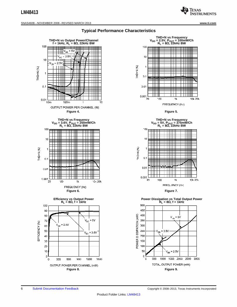
Typical Performance Characteristics
THD+N vs FrequencyTHD+N vs Output Power/Channel VDD = 2.5V, POUT = 100mW/Ch
f = 1kHz, RL = 8Ω, 22kHz BW RL = 8Ω, 22kHz BW
Figure 4. Figure 5.
THD+N vs Frequency THD+N vs FrequencyVDD = 3.6V, POUT = 250mW/Ch VDD = 5V, POUT = 375mW/Ch
RL = 8Ω, 22kHz BW RL = 8Ω, 22kHz BW
Figure 6. Figure 7.
Efficiency vs Output Power Power Dissipation vs Total Output PowerRL = 8Ω, f = 1kHz RL = 8Ω, f = 1kHz
Figure 8. Figure 9.
6 Submit Documentation Feedback Copyright © 2008–2013, Texas Instruments Incorporated
Product Folder Links: LM48413
LM48413
www.ti.com SNAS460B –NOVEMBER 2008–REVISED MARCH 2013
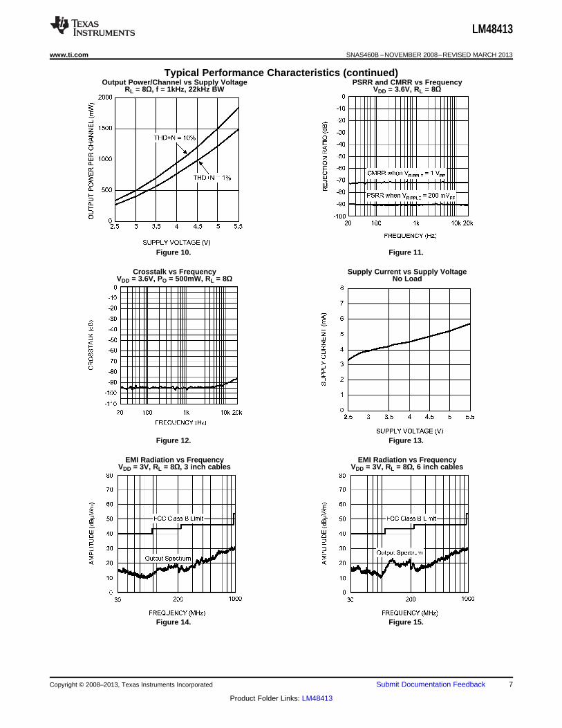
Typical Performance Characteristics (continued)Output Power/Channel vs Supply Voltage PSRR and CMRR vs Frequency
RL = 8Ω, f = 1kHz, 22kHz BW VDD = 3.6V, RL = 8Ω
Figure 10. Figure 11.
Crosstalk vs Frequency Supply Current vs Supply VoltageVDD = 3.6V, PO = 500mW, RL = 8Ω No Load
Figure 12. Figure 13.
EMI Radiation vs Frequency EMI Radiation vs FrequencyVDD = 3V, RL = 8Ω, 3 inch cables VDD = 3V, RL = 8Ω, 6 inch cables
Figure 14. Figure 15.
Copyright © 2008–2013, Texas Instruments Incorporated Submit Documentation Feedback 7
Product Folder Links: LM48413
LM48413
SNAS460B –NOVEMBER 2008–REVISED MARCH 2013 www.ti.com
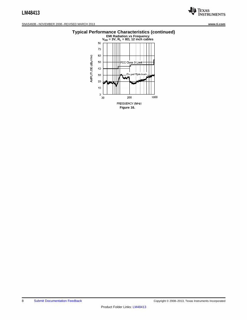
Typical Performance Characteristics (continued)EMI Radiation vs Frequency
VDD = 3V, RL = 8Ω, 12 inch cables
Figure 16.
8 Submit Documentation Feedback Copyright © 2008–2013, Texas Instruments Incorporated
Product Folder Links: LM48413
LM48413
www.ti.com SNAS460B –NOVEMBER 2008–REVISED MARCH 2013
APPLICATION INFORMATION
GENERAL AMPLIFIER FUNCTION
The LM48413 stereo Class D audio power amplifier features a filterless modulation scheme that reduces externalcomponent count, conserving board space and reducing system cost. The outputs of the device transition fromPVDD to GND with a 390kHz switching frequency. With no signal applied, the outputs switch with a 50% dutycycle, in phase, causing the two outputs to cancel. This cancellation results in no net voltage across the speaker,thus there is no current to the load in the idle state.
When an input signal is applied, the duty cycle (pulse width) of the LM48413 output's change. For increasingoutput voltage, the duty cycle of one side of each output increases, while the duty cycle of the other side of eachoutput decreases. For decreasing output voltages, the converse occurs. The difference between the two pulsewidths yields the differential output voltage.
SHUTDOWN FUNCTION
The LM48413 features a low current shutdown mode. Set SD = GND to disable the amplifier and reduce supplycurrent to 0.03μA.
Switch SD between GND and VDD for minimum current consumption in shutdown. The LM48413 may bedisabled with shutdown voltages in between GND and VDD, but the idle current will be greater than the typicalvalue. The LM48413 shutdown input has an internal 300kΩ pull-down resistor. The purpose of this resistor is toeliminate any unwanted state changes when this pin is floating. To minimize shutdown current, it should bedriven to GND or left floating. If it is not driven to GND, or floating, a small increase in shutdown supply currentwill be noticed.
SPREAD SPECTRUM
The LM48413 outputs are modulated in spread spectrum scheme eliminating the need for output filters, ferritebeads or chokes. During its operation, the switching frequency varies randomly by 30% about a 390kHz centerfrequency, reducing the wideband spectral content and improving EMI emissions radiated by the speaker andassociated cables and traces. A fixed frequency class D exhibits large amounts of spectral energy at multiples ofthe switching frequency. The spread spectrum architecture of the LM48413 spreads the same energy over alarger bandwidth. The cycle-to-cycle variation of the switching period does not affect the audio reproduction,efficiency, or PSRR.
ENHANCED EMISSIONS SUPPRESSION SYSTEM (E2S)
The LM48413 features Texas Instruments’ patented E2S system that further reduces EMI, while maintaining highquality audio reproduction and efficiency. The advanced edge rate control (ERC) embedded within the E2Ssystem works simultaneously with the spread spectrum already activated. The LM48413 ERC greatly reducesthe high frequency components of the output square waves by controlling the output rise and fall times, slowingthe transitions to reduce RF emissions, while maximizing THD+N and efficiency performance.
DIFFERENTIAL AMPLIFIER EXPLANATION
As logic supplies continue to shrink, system designers are increasingly turning to differential analog signalhandling to preserve signal to noise ratios with restricted voltage swings. The LM48413 features two fullydifferential speaker amplifiers. A differential amplifier amplifies the difference between the two input signals.Traditional audio power amplifiers have typically offered only single-ended inputs resulting in a 6dB reduction ofSNR relative to differential inputs. The LM48413 also offers the possibility of DC input coupling which eliminatesthe input coupling capacitors. A major benefit of the fully differential amplifier is the improved common moderejection ratio (CMRR) over single-ended input amplifiers. The increased CMRR of the differential amplifierreduces sensitivity to ground offset related noise injection, especially important in noisy systems.
POWER DISSIPATION AND EFFICIENCY
The major benefit of a Class D amplifier is increased efficiency versus a Class AB. The efficiency of theLM48413 is attributed to the region of operation of the transistors in the output stage. The Class D output stageacts as current steering switches, consuming negligible amounts of power compared to a Class AB amplifier.Most of the power loss associated with the output stage is due to the IR loss of the MOSFET on-resistance,along with switching losses due to gate charge.
Copyright © 2008–2013, Texas Instruments Incorporated Submit Documentation Feedback 9
Product Folder Links: LM48413
LM48413
SNAS460B –NOVEMBER 2008–REVISED MARCH 2013 www.ti.com
PROPER SELECTION OF EXTERNAL COMPONENTS
Power Supply Bypassing/Filtering
Proper power supply bypassing is important for low noise performance and high PSRR. Place the 1μF supplybypass capacitor as close to the device as possible. Traditionally, a pair of bypass capacitors with typical value0.1μF and 10μF are applied to the supply rail for increasing stability. Nevertheless, these capacitors do noteliminate the need for bypassing of the LM48413 supply pins.
Input Capacitor Selection
Input capacitors may be required for some applications, or when the audio source is single-ended. Inputcapacitors block the DC component of the audio signal, eliminating any conflict between the DC component ofthe audio source and the bias voltage of the LM48413. The input capacitors create a high-pass filter with theinput resistance RIN. The -3dB point of the high-pass filter is found using Equation 1 below.
f = 1 / 2πRINCIN (Hz) (1)
The input capacitors can also be used to remove low frequency content from the audio signal. When theLM48413 is using a single-ended source, power supply noise on the ground is seen as an input signal. Settingthe high-pass filter point above the power supply noise frequencies, 217Hz in a GSM phone, for example, filtersout the noise such that it is not amplified and heard on the output. Capacitors with a tolerance of 10% or betterare recommended for impedance matching and improved CMRR and PSRR.
Texas Instruments 3D Enhancement
The LM48413 features Texas Instruments' 3D enhancement effect that widens the perceived soundstage of astereo audio signal. The 3D enhancement increases the apparent stereo channel separation, improving audioreproduction whenever the left and right speakers are too close to one another.
An external RC network shown in Figure 2 is required to enable the 3D effect. Because the LM48413 is a fullydifferential amplifier, there are two separate RC networks, one for each stereo input pair (INL+ and INR+, andINL- and INR-). Set 3DEN high to enable the 3D effect. Set 3DEN low to disable the 3D effect.
The 3D RC network acts as a high-pass filter. The amount of the 3D effect is set by the R3D resistor. Decreasingthe value of R3D increases the 3D effect. The C3D capacitor sets the frequency at which the 3D effect occurs.Increasing the value of C3D decreases the low frequency cutoff point, extending the 3D effect over a widerbandwidth. The low frequency cutoff point is given by Equation 2:
f3D(–3dB) = 1 / 2π(R3D)(C3D) (Hz) (2)
Enabling the 3D effect increase the gain by a factor of (1+40kΩ/R3D). Setting R3D to 40kΩ results in a gainincrease of 6dB whenever the 3D effect is enabled. The Equation 2 holds for both differential and single-endconfiguration. The recommended tolerance of the resistor value and capacitor value of the two RC networks are5% and 10% respectively. Tolerance out of this range may affect the 3D gain and low frequency cut-off point toomuch. The desired sound quality of the 3D effect may not be obtained consequently.
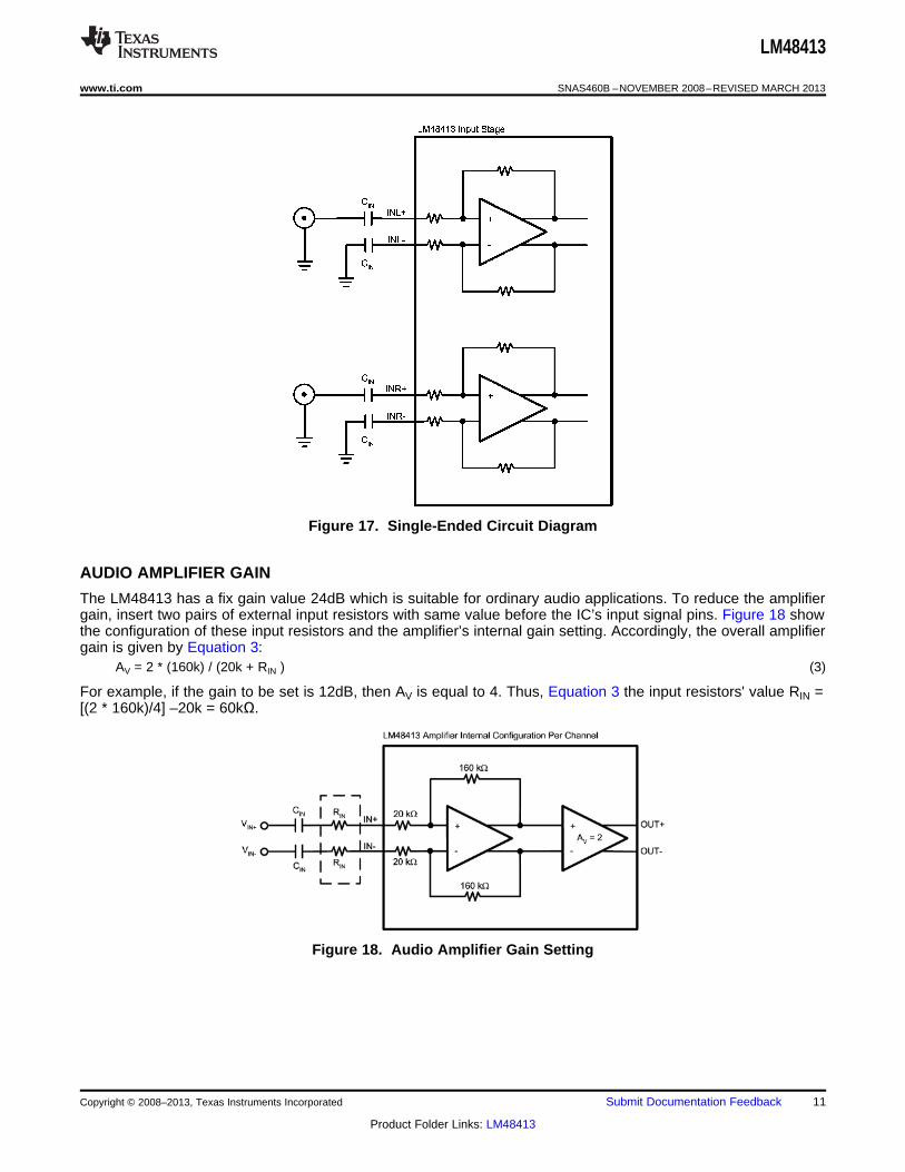
SINGLE-ENDED AUDIO AMPLIFIER CONFIGURATION
The LM48413 is compatible with single-ended sources. When configured for single-ended inputs, inputcapacitors must be used to block and DC component at the input of the device. Figure 17 shows the typicalsingle-ended applications circuit.
10 Submit Documentation Feedback Copyright © 2008–2013, Texas Instruments Incorporated
Product Folder Links: LM48413
LM48413
www.ti.com SNAS460B –NOVEMBER 2008–REVISED MARCH 2013
Figure 17. Single-Ended Circuit Diagram
AUDIO AMPLIFIER GAIN
The LM48413 has a fix gain value 24dB which is suitable for ordinary audio applications. To reduce the amplifiergain, insert two pairs of external input resistors with same value before the IC’s input signal pins. Figure 18 showthe configuration of these input resistors and the amplifier’s internal gain setting. Accordingly, the overall amplifiergain is given by Equation 3:
AV = 2 * (160k) / (20k + RIN ) (3)
For example, if the gain to be set is 12dB, then AV is equal to 4. Thus, Equation 3 the input resistors' value RIN =[(2 * 160k)/4] –20k = 60kΩ.
Figure 18. Audio Amplifier Gain Setting
Copyright © 2008–2013, Texas Instruments Incorporated Submit Documentation Feedback 11
Product Folder Links: LM48413
LM48413
SNAS460B –NOVEMBER 2008–REVISED MARCH 2013 www.ti.com
PCB LAYOUT GUIDELINES
As output power increases, interconnect resistance (PCB traces and wires) between the amplifier, load andpower supply create a voltage drop. The voltage loss due to the traces between the LM48413 and the loadresults in lower output power and decreased efficiency. Higher trace resistance between the supply and theLM48413 has the same effect as a poorly regulated supply, increasing ripple on the supply line, and reducingpeak output power. The effects of residual trace resistance increases as output current increases due to higheroutput power, decreased load impedance or both. To maintain the highest output voltage swing andcorresponding peak output power, the PCB traces that connect the output pins to the load and the supply pins tothe power supply should be as wide as possible to minimize trace resistance.
The use of power and ground planes will give the best THD+N performance. In addition to reducing traceresistance, the use of power planes creates parasitic capacitors that help to filter the power supply line.
The inductive nature of the transducer load can also result in overshoot on one or both edges, clamped by theparasitic diodes to GND and VDD in each case. From an EMI standpoint, this is an aggressive waveform that canradiate or conduct to other components in the system and cause interference. It is essential to keep the powerand output traces short and well shielded if possible. Use of ground planes beads and micros-strip layouttechniques are all useful in preventing unwanted interference.
As the distance from the LM48413 and the speaker increases, the amount of EMI radiation increases due to theoutput wires or traces acting as antennas. The EMI output spectrums of LM48413 evaluation board connectedwith different speaker cable lengths to an 8Ω load were measured (See Typical Performance Characteristics).Lengths from 3 inches to 12 inches are shown all fall within the limit of the FCC Class B requirement.
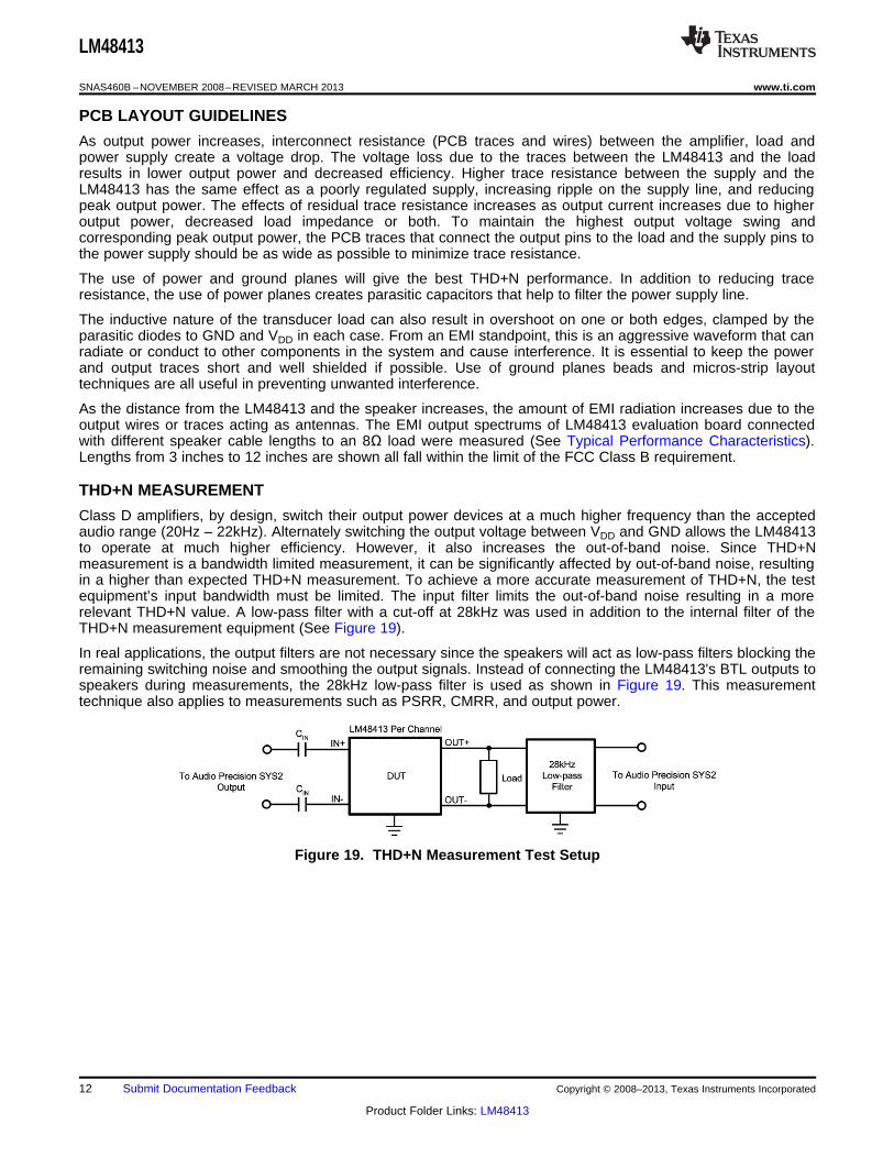
THD+N MEASUREMENT
Class D amplifiers, by design, switch their output power devices at a much higher frequency than the acceptedaudio range (20Hz – 22kHz). Alternately switching the output voltage between VDD and GND allows the LM48413to operate at much higher efficiency. However, it also increases the out-of-band noise. Since THD+Nmeasurement is a bandwidth limited measurement, it can be significantly affected by out-of-band noise, resultingin a higher than expected THD+N measurement. To achieve a more accurate measurement of THD+N, the testequipment’s input bandwidth must be limited. The input filter limits the out-of-band noise resulting in a morerelevant THD+N value. A low-pass filter with a cut-off at 28kHz was used in addition to the internal filter of theTHD+N measurement equipment (See Figure 19).
In real applications, the output filters are not necessary since the speakers will act as low-pass filters blocking theremaining switching noise and smoothing the output signals. Instead of connecting the LM48413's BTL outputs tospeakers during measurements, the 28kHz low-pass filter is used as shown in Figure 19. This measurementtechnique also applies to measurements such as PSRR, CMRR, and output power.
Figure 19. THD+N Measurement Test Setup
12 Submit Documentation Feedback Copyright © 2008–2013, Texas Instruments Incorporated
Product Folder Links: LM48413
LM48413
www.ti.com SNAS460B –NOVEMBER 2008–REVISED MARCH 2013
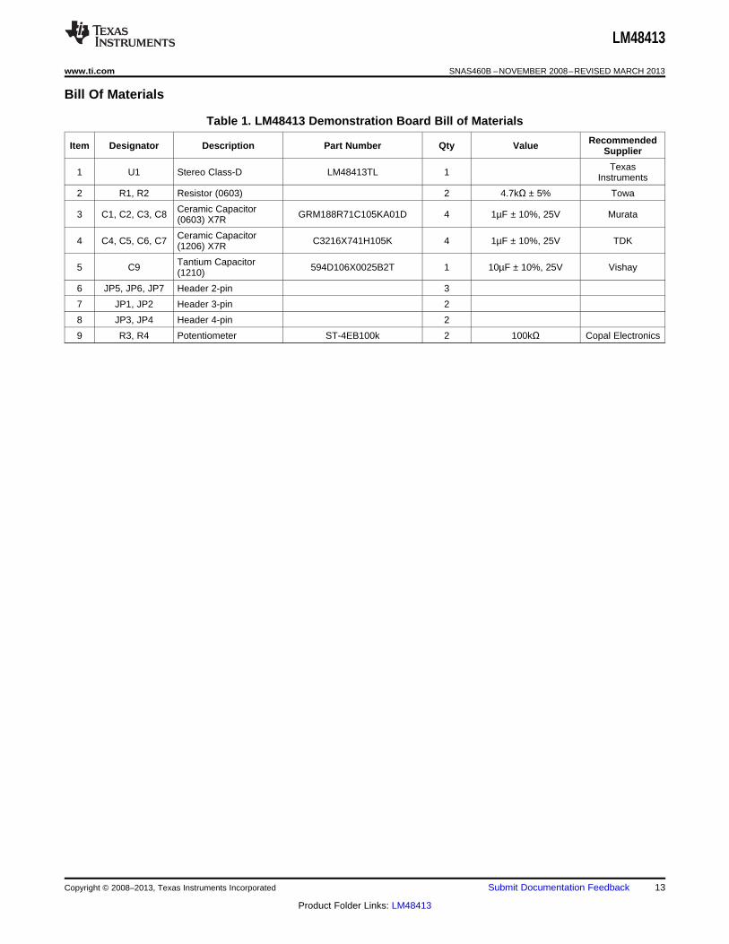
Bill Of Materials
Table 1. LM48413 Demonstration Board Bill of Materials
RecommendedItem Designator Description Part Number Qty Value Supplier
Texas1 U1 Stereo Class-D LM48413TL 1 Instruments
2 R1, R2 Resistor (0603) 2 4.7kΩ ± 5% Towa
Ceramic Capacitor3 C1, C2, C3, C8 GRM188R71C105KA01D 4 1µF ± 10%, 25V Murata(0603) X7R
Ceramic Capacitor4 C4, C5, C6, C7 C3216X741H105K 4 1µF ± 10%, 25V TDK(1206) X7R
Tantium Capacitor5 C9 594D106X0025B2T 1 10µF ± 10%, 25V Vishay(1210)
6 JP5, JP6, JP7 Header 2-pin 3
7 JP1, JP2 Header 3-pin 2
8 JP3, JP4 Header 4-pin 2
9 R3, R4 Potentiometer ST-4EB100k 2 100kΩ Copal Electronics
Copyright © 2008–2013, Texas Instruments Incorporated Submit Documentation Feedback 13
Product Folder Links: LM48413
LM48413
SNAS460B –NOVEMBER 2008–REVISED MARCH 2013 www.ti.com
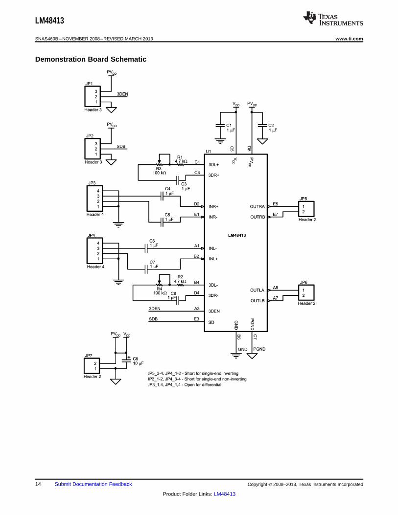
Demonstration Board Schematic
14 Submit Documentation Feedback Copyright © 2008–2013, Texas Instruments Incorporated
Product Folder Links: LM48413
LM48413
www.ti.com SNAS460B –NOVEMBER 2008–REVISED MARCH 2013
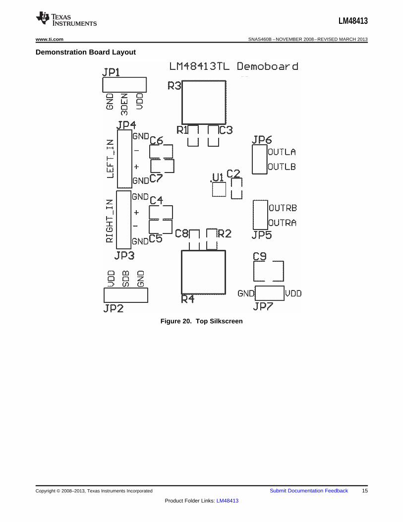
Demonstration Board Layout
Figure 20. Top Silkscreen
Copyright © 2008–2013, Texas Instruments Incorporated Submit Documentation Feedback 15
Product Folder Links: LM48413
LM48413
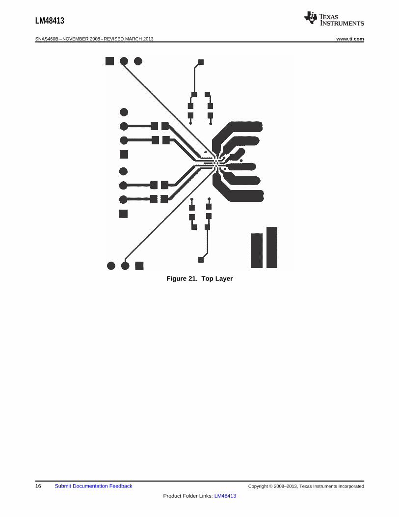
SNAS460B –NOVEMBER 2008–REVISED MARCH 2013 www.ti.com
Figure 21. Top Layer
16 Submit Documentation Feedback Copyright © 2008–2013, Texas Instruments Incorporated
Product Folder Links: LM48413
LM48413
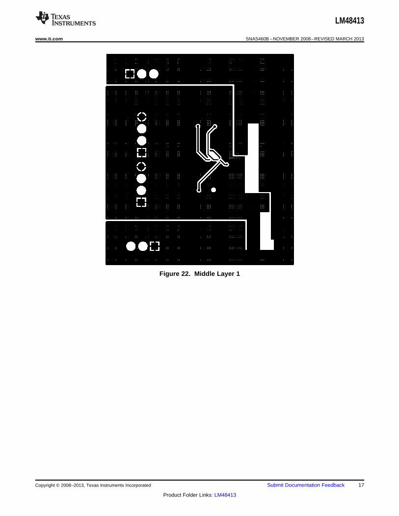
www.ti.com SNAS460B –NOVEMBER 2008–REVISED MARCH 2013
Figure 22. Middle Layer 1
Copyright © 2008–2013, Texas Instruments Incorporated Submit Documentation Feedback 17
Product Folder Links: LM48413
LM48413
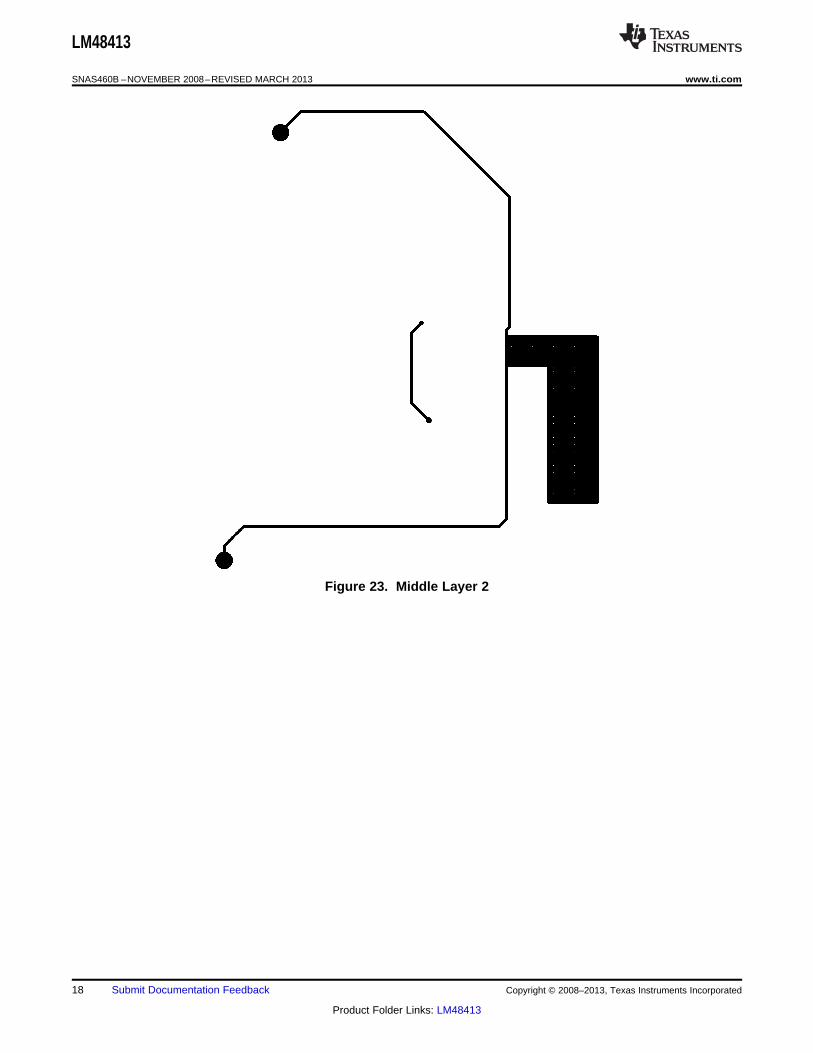
SNAS460B –NOVEMBER 2008–REVISED MARCH 2013 www.ti.com
Figure 23. Middle Layer 2
18 Submit Documentation Feedback Copyright © 2008–2013, Texas Instruments Incorporated
Product Folder Links: LM48413
LM48413
www.ti.com SNAS460B –NOVEMBER 2008–REVISED MARCH 2013
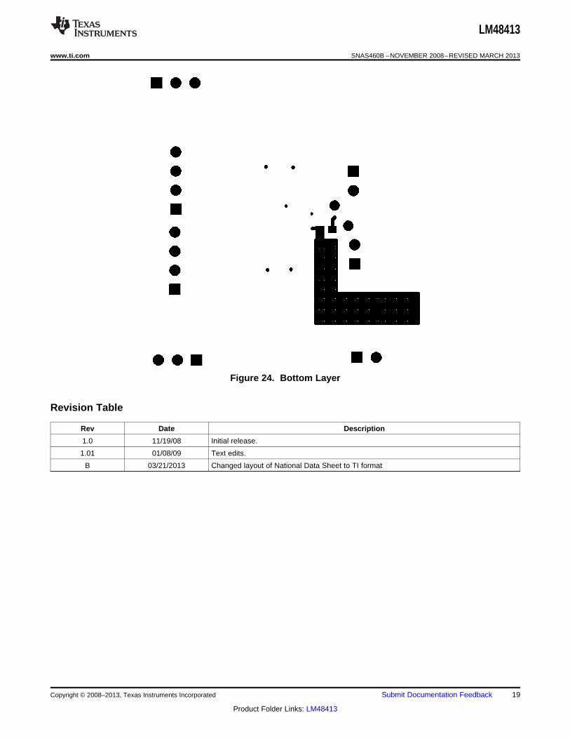
Figure 24. Bottom Layer
Revision Table
Rev Date Description
1.0 11/19/08 Initial release.
1.01 01/08/09 Text edits.
B 03/21/2013 Changed layout of National Data Sheet to TI format
Copyright © 2008–2013, Texas Instruments Incorporated Submit Documentation Feedback 19
Product Folder Links: LM48413
PACKAGE OPTION ADDENDUM
www.ti.com 24-Sep-2015
Addendum-Page 1
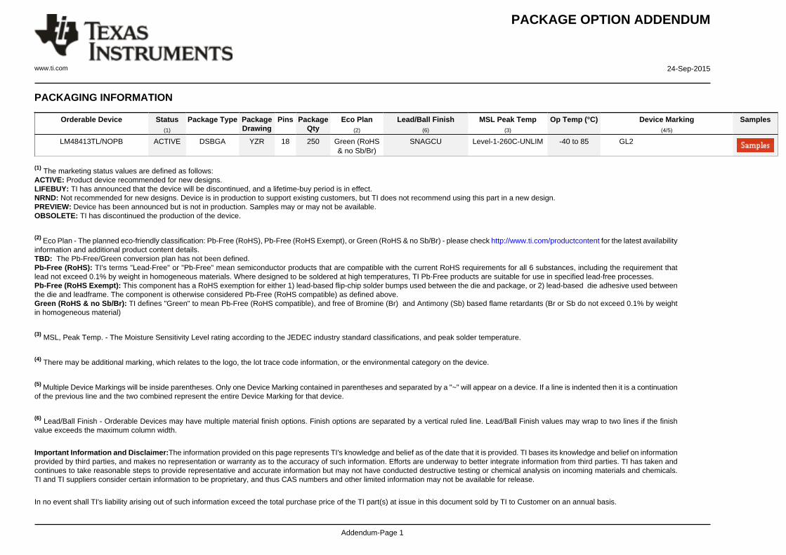
PACKAGING INFORMATION
Orderable Device Status(1)
Package Type PackageDrawing
Pins PackageQty
Eco Plan(2)
Lead/Ball Finish(6)
MSL Peak Temp(3)
Op Temp (°C) Device Marking(4/5)
Samples
LM48413TL/NOPB ACTIVE DSBGA YZR 18 250 Green (RoHS& no Sb/Br)
SNAGCU Level-1-260C-UNLIM -40 to 85 GL2
(1) The marketing status values are defined as follows:ACTIVE: Product device recommended for new designs.LIFEBUY: TI has announced that the device will be discontinued, and a lifetime-buy period is in effect.NRND: Not recommended for new designs. Device is in production to support existing customers, but TI does not recommend using this part in a new design.PREVIEW: Device has been announced but is not in production. Samples may or may not be available.OBSOLETE: TI has discontinued the production of the device.
(2) Eco Plan - The planned eco-friendly classification: Pb-Free (RoHS), Pb-Free (RoHS Exempt), or Green (RoHS & no Sb/Br) - please check http://www.ti.com/productcontent for the latest availabilityinformation and additional product content details.TBD: The Pb-Free/Green conversion plan has not been defined.Pb-Free (RoHS): TI's terms "Lead-Free" or "Pb-Free" mean semiconductor products that are compatible with the current RoHS requirements for all 6 substances, including the requirement thatlead not exceed 0.1% by weight in homogeneous materials. Where designed to be soldered at high temperatures, TI Pb-Free products are suitable for use in specified lead-free processes.Pb-Free (RoHS Exempt): This component has a RoHS exemption for either 1) lead-based flip-chip solder bumps used between the die and package, or 2) lead-based die adhesive used betweenthe die and leadframe. The component is otherwise considered Pb-Free (RoHS compatible) as defined above.Green (RoHS & no Sb/Br): TI defines "Green" to mean Pb-Free (RoHS compatible), and free of Bromine (Br) and Antimony (Sb) based flame retardants (Br or Sb do not exceed 0.1% by weightin homogeneous material)
(3) MSL, Peak Temp. - The Moisture Sensitivity Level rating according to the JEDEC industry standard classifications, and peak solder temperature.
(4) There may be additional marking, which relates to the logo, the lot trace code information, or the environmental category on the device.
(5) Multiple Device Markings will be inside parentheses. Only one Device Marking contained in parentheses and separated by a "~" will appear on a device. If a line is indented then it is a continuationof the previous line and the two combined represent the entire Device Marking for that device.
(6) Lead/Ball Finish - Orderable Devices may have multiple material finish options. Finish options are separated by a vertical ruled line. Lead/Ball Finish values may wrap to two lines if the finishvalue exceeds the maximum column width.
Important Information and Disclaimer:The information provided on this page represents TI's knowledge and belief as of the date that it is provided. TI bases its knowledge and belief on informationprovided by third parties, and makes no representation or warranty as to the accuracy of such information. Efforts are underway to better integrate information from third parties. TI has taken andcontinues to take reasonable steps to provide representative and accurate information but may not have conducted destructive testing or chemical analysis on incoming materials and chemicals.TI and TI suppliers consider certain information to be proprietary, and thus CAS numbers and other limited information may not be available for release.
In no event shall TI's liability arising out of such information exceed the total purchase price of the TI part(s) at issue in this document sold by TI to Customer on an annual basis.
PACKAGE OPTION ADDENDUM
www.ti.com 24-Sep-2015
Addendum-Page 2
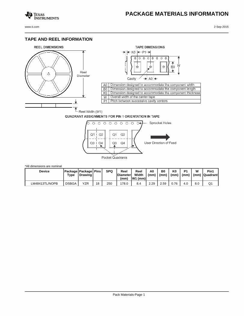
TAPE AND REEL INFORMATION
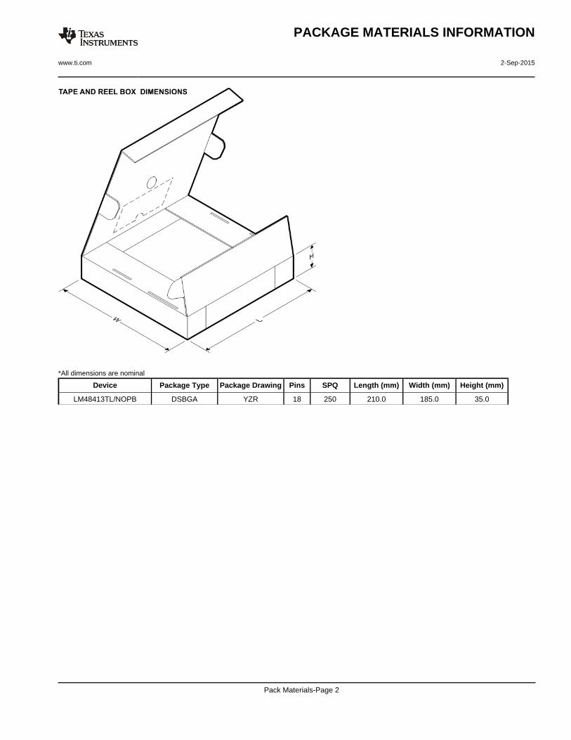
*All dimensions are nominal
Device PackageType
PackageDrawing
Pins SPQ ReelDiameter
(mm)
ReelWidth
W1 (mm)
A0(mm)
B0(mm)
K0(mm)
P1(mm)
W(mm)
Pin1Quadrant
LM48413TL/NOPB DSBGA YZR 18 250 178.0 8.4 2.29 2.59 0.76 4.0 8.0 Q1
PACKAGE MATERIALS INFORMATION
www.ti.com 2-Sep-2015
Pack Materials-Page 1
*All dimensions are nominal
Device Package Type Package Drawing Pins SPQ Length (mm) Width (mm) Height (mm)
LM48413TL/NOPB DSBGA YZR 18 250 210.0 185.0 35.0
PACKAGE MATERIALS INFORMATION
www.ti.com 2-Sep-2015
Pack Materials-Page 2
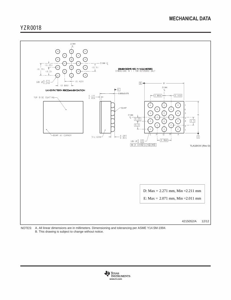
MECHANICAL DATA
YZR0018xxx
www.ti.com
TLA18XXX (Rev D)
0.600±0.075
D
E
A. All linear dimensions are in millimeters. Dimensioning and tolerancing per ASME Y14.5M-1994.B. This drawing is subject to change without notice.
4215052/A 12/12
NOTES:
D: Max =
E: Max =
2.271 mm, Min =
2.071 mm, Min =
2.211 mm
2.011 mm
IMPORTANT NOTICE
Texas Instruments Incorporated (TI) reserves the right to make corrections, enhancements, improvements and other changes to itssemiconductor products and services per JESD46, latest issue, and to discontinue any product or service per JESD48, latest issue. Buyersshould obtain the latest relevant information before placing orders and should verify that such information is current and complete.TI’s published terms of sale for semiconductor products (http://www.ti.com/sc/docs/stdterms.htm) apply to the sale of packaged integratedcircuit products that TI has qualified and released to market. Additional terms may apply to the use or sale of other types of TI products andservices.Reproduction of significant portions of TI information in TI data sheets is permissible only if reproduction is without alteration and isaccompanied by all associated warranties, conditions, limitations, and notices. TI is not responsible or liable for such reproduceddocumentation. Information of third parties may be subject to additional restrictions. Resale of TI products or services with statementsdifferent from or beyond the parameters stated by TI for that product or service voids all express and any implied warranties for theassociated TI product or service and is an unfair and deceptive business practice. TI is not responsible or liable for any such statements.Buyers and others who are developing systems that incorporate TI products (collectively, “Designers”) understand and agree that Designersremain responsible for using their independent analysis, evaluation and judgment in designing their applications and that Designers havefull and exclusive responsibility to assure the safety of Designers' applications and compliance of their applications (and of all TI productsused in or for Designers’ applications) with all applicable regulations, laws and other applicable requirements. Designer represents that, withrespect to their applications, Designer has all the necessary expertise to create and implement safeguards that (1) anticipate dangerousconsequences of failures, (2) monitor failures and their consequences, and (3) lessen the likelihood of failures that might cause harm andtake appropriate actions. Designer agrees that prior to using or distributing any applications that include TI products, Designer willthoroughly test such applications and the functionality of such TI products as used in such applications.TI’s provision of technical, application or other design advice, quality characterization, reliability data or other services or information,including, but not limited to, reference designs and materials relating to evaluation modules, (collectively, “TI Resources”) are intended toassist designers who are developing applications that incorporate TI products; by downloading, accessing or using TI Resources in anyway, Designer (individually or, if Designer is acting on behalf of a company, Designer’s company) agrees to use any particular TI Resourcesolely for this purpose and subject to the terms of this Notice.TI’s provision of TI Resources does not expand or otherwise alter TI’s applicable published warranties or warranty disclaimers for TIproducts, and no additional obligations or liabilities arise from TI providing such TI Resources. TI reserves the right to make corrections,enhancements, improvements and other changes to its TI Resources. TI has not conducted any testing other than that specificallydescribed in the published documentation for a particular TI Resource.Designer is authorized to use, copy and modify any individual TI Resource only in connection with the development of applications thatinclude the TI product(s) identified in such TI Resource. NO OTHER LICENSE, EXPRESS OR IMPLIED, BY ESTOPPEL OR OTHERWISETO ANY OTHER TI INTELLECTUAL PROPERTY RIGHT, AND NO LICENSE TO ANY TECHNOLOGY OR INTELLECTUAL PROPERTYRIGHT OF TI OR ANY THIRD PARTY IS GRANTED HEREIN, including but not limited to any patent right, copyright, mask work right, orother intellectual property right relating to any combination, machine, or process in which TI products or services are used. Informationregarding or referencing third-party products or services does not constitute a license to use such products or services, or a warranty orendorsement thereof. Use of TI Resources may require a license from a third party under the patents or other intellectual property of thethird party, or a license from TI under the patents or other intellectual property of TI.TI RESOURCES ARE PROVIDED “AS IS” AND WITH ALL FAULTS. TI DISCLAIMS ALL OTHER WARRANTIES ORREPRESENTATIONS, EXPRESS OR IMPLIED, REGARDING RESOURCES OR USE THEREOF, INCLUDING BUT NOT LIMITED TOACCURACY OR COMPLETENESS, TITLE, ANY EPIDEMIC FAILURE WARRANTY AND ANY IMPLIED WARRANTIES OFMERCHANTABILITY, FITNESS FOR A PARTICULAR PURPOSE, AND NON-INFRINGEMENT OF ANY THIRD PARTY INTELLECTUALPROPERTY RIGHTS. TI SHALL NOT BE LIABLE FOR AND SHALL NOT DEFEND OR INDEMNIFY DESIGNER AGAINST ANY CLAIM,INCLUDING BUT NOT LIMITED TO ANY INFRINGEMENT CLAIM THAT RELATES TO OR IS BASED ON ANY COMBINATION OFPRODUCTS EVEN IF DESCRIBED IN TI RESOURCES OR OTHERWISE. IN NO EVENT SHALL TI BE LIABLE FOR ANY ACTUAL,DIRECT, SPECIAL, COLLATERAL, INDIRECT, PUNITIVE, INCIDENTAL, CONSEQUENTIAL OR EXEMPLARY DAMAGES INCONNECTION WITH OR ARISING OUT OF TI RESOURCES OR USE THEREOF, AND REGARDLESS OF WHETHER TI HAS BEENADVISED OF THE POSSIBILITY OF SUCH DAMAGES.Unless TI has explicitly designated an individual product as meeting the requirements of a particular industry standard (e.g., ISO/TS 16949and ISO 26262), TI is not responsible for any failure to meet such industry standard requirements.Where TI specifically promotes products as facilitating functional safety or as compliant with industry functional safety standards, suchproducts are intended to help enable customers to design and create their own applications that meet applicable functional safety standardsand requirements. Using products in an application does not by itself establish any safety features in the application. Designers mustensure compliance with safety-related requirements and standards applicable to their applications. Designer may not use any TI products inlife-critical medical equipment unless authorized officers of the parties have executed a special contract specifically governing such use.Life-critical medical equipment is medical equipment where failure of such equipment would cause serious bodily injury or death (e.g., lifesupport, pacemakers, defibrillators, heart pumps, neurostimulators, and implantables). Such equipment includes, without limitation, allmedical devices identified by the U.S. Food and Drug Administration as Class III devices and equivalent classifications outside the U.S.TI may expressly designate certain products as completing a particular qualification (e.g., Q100, Military Grade, or Enhanced Product).Designers agree that it has the necessary expertise to select the product with the appropriate qualification designation for their applicationsand that proper product selection is at Designers’ own risk. Designers are solely responsible for compliance with all legal and regulatoryrequirements in connection with such selection.Designer will fully indemnify TI and its representatives against any damages, costs, losses, and/or liabilities arising out of Designer’s non-compliance with the terms and provisions of this Notice.
Mailing Address: Texas Instruments, Post Office Box 655303, Dallas, Texas 75265Copyright © 2017, Texas Instruments Incorporated