LM4871 3W Audio Power Amplifier with Shutdown Mode (Rev. F)
24
LM4871 www.ti.com SNAS002F – FEBRUARY 2000 – REVISED MAY 2013 LM4871 3W Audio Power Amplifier with Shutdown Mode Check for Samples: LM4871 1FEATURES DESCRIPTION The LM4871 is a mono bridged audio power amplifier 2• No Output Coupling Capacitors, Bootstrap capable of delivering 3W of continuous average Capacitors, or Snubber Circuits Required power into a 3Ω load with less than 10% THD when • Unity-gain Stable powered by a 5V power supply (see Note). To • WSON, VSSOP, SOIC, or PDIP Packaging conserve power in portable applications, the LM4871's micropower shutdown mode (I Q = 0.6μA, • External Gain Configuration Capability typ) is activated when V DD is applied to the • Pin Compatible with the LM4861 SHUTDOWN pin. Boomer audio power amplifiers are designed APPLICATIONS specifically to provide high power, high fidelity audio • Portable Computers output. They require few external components and • Desktop Computers operate on low supply voltages from 2.0V to 5.5V. Since the LM4871 does not require output coupling • Low Voltage Audio Systems capacitors, bootstrap capacitors, or snubber networks, it is ideally suited for low-power portable KEY SPECIFICATIONS systems that require minimum volume and weight. • PO at 10% THD+N, 1kHz Additional LM4871 features include thermal shutdown – LM4871LD: 3Ω ,4Ω Loads; 3W (typ), protection, unity-gain stability, and external gain set. 2.5 W (typ) Note: An LM4871LD that has been properly mounted – All other LM4871 Packages: 8Ω load to a circuit board will deliver 3W into 3Ω (at 10% 1.5 W (typ) THD). The other package options for the LM4871 will • Shutdown Current 0.6μA (typ) deliver 1.5W into 8Ω (at 10% THD). See the Application Information section for further information • Supply Voltage Range 2.0V to 5.5 V concerning the LM4871LD, LM4871MM, LM4871M, • THD at 1kHz at 1W Continuous Average and the LM4871N. Output Power into 8Ω 0.5% (max) Connection Diagrams Figure 1. VSSOP, Small Outline, and PDIP Figure 2. WSON Package (Top View) Package See Package Number NGN0008A Top View See Package Number DGK0008A, D0008A, or D0008E 1 Please be aware that an important notice concerning availability, standard warranty, and use in critical applications of Texas Instruments semiconductor products and disclaimers thereto appears at the end of this data sheet. 2All trademarks are the property of their respective owners. PRODUCTION DATA information is current as of publication date. Copyright © 2000–2013, Texas Instruments Incorporated Products conform to specifications per the terms of the Texas Instruments standard warranty. Production processing does not necessarily include testing of all parameters.
Transcript of LM4871 3W Audio Power Amplifier with Shutdown Mode (Rev. F)
LM4871
www.ti.com SNAS002F –FEBRUARY 2000–REVISED MAY 2013
LM4871 3W Audio Power Amplifier with Shutdown ModeCheck for Samples: LM4871
1FEATURES DESCRIPTIONThe LM4871 is a mono bridged audio power amplifier
2• No Output Coupling Capacitors, Bootstrapcapable of delivering 3W of continuous averageCapacitors, or Snubber Circuits Requiredpower into a 3Ω load with less than 10% THD when
• Unity-gain Stable powered by a 5V power supply (see Note). To• WSON, VSSOP, SOIC, or PDIP Packaging conserve power in portable applications, the
LM4871's micropower shutdown mode (IQ = 0.6µA,• External Gain Configuration Capabilitytyp) is activated when VDD is applied to the
• Pin Compatible with the LM4861 SHUTDOWN pin.
Boomer audio power amplifiers are designedAPPLICATIONSspecifically to provide high power, high fidelity audio
• Portable Computers output. They require few external components and• Desktop Computers operate on low supply voltages from 2.0V to 5.5V.
Since the LM4871 does not require output coupling• Low Voltage Audio Systemscapacitors, bootstrap capacitors, or snubbernetworks, it is ideally suited for low-power portableKEY SPECIFICATIONS systems that require minimum volume and weight.
• PO at 10% THD+N, 1kHzAdditional LM4871 features include thermal shutdown
– LM4871LD: 3Ω , 4Ω Loads; 3W (typ), protection, unity-gain stability, and external gain set.2.5 W (typ)
Note: An LM4871LD that has been properly mounted– All other LM4871 Packages: 8Ω load to a circuit board will deliver 3W into 3Ω (at 10%
1.5 W (typ) THD). The other package options for the LM4871 will• Shutdown Current 0.6µA (typ) deliver 1.5W into 8Ω (at 10% THD). See the
Application Information section for further information• Supply Voltage Range 2.0V to 5.5 Vconcerning the LM4871LD, LM4871MM, LM4871M,
• THD at 1kHz at 1W Continuous Average and the LM4871N.Output Power into 8Ω 0.5% (max)
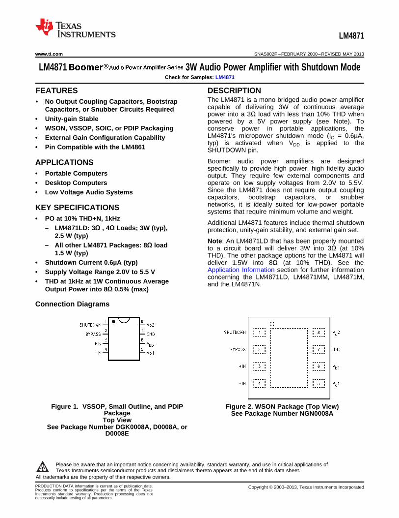
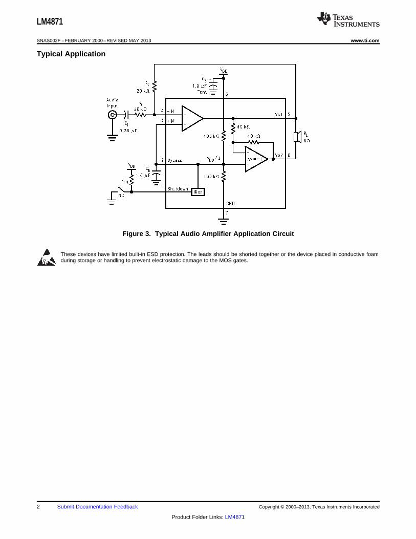
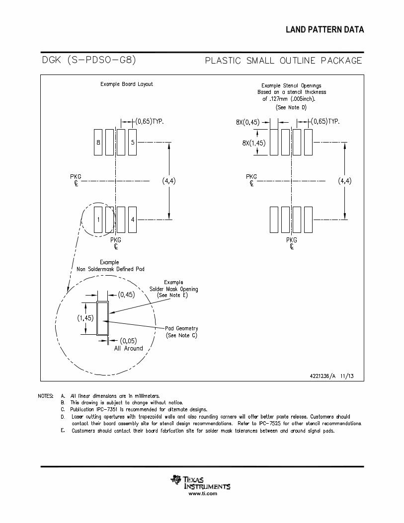
Connection Diagrams
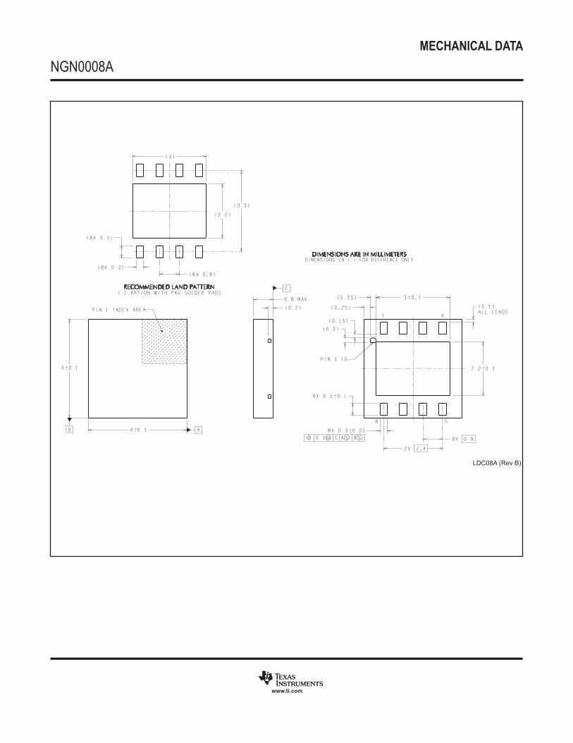
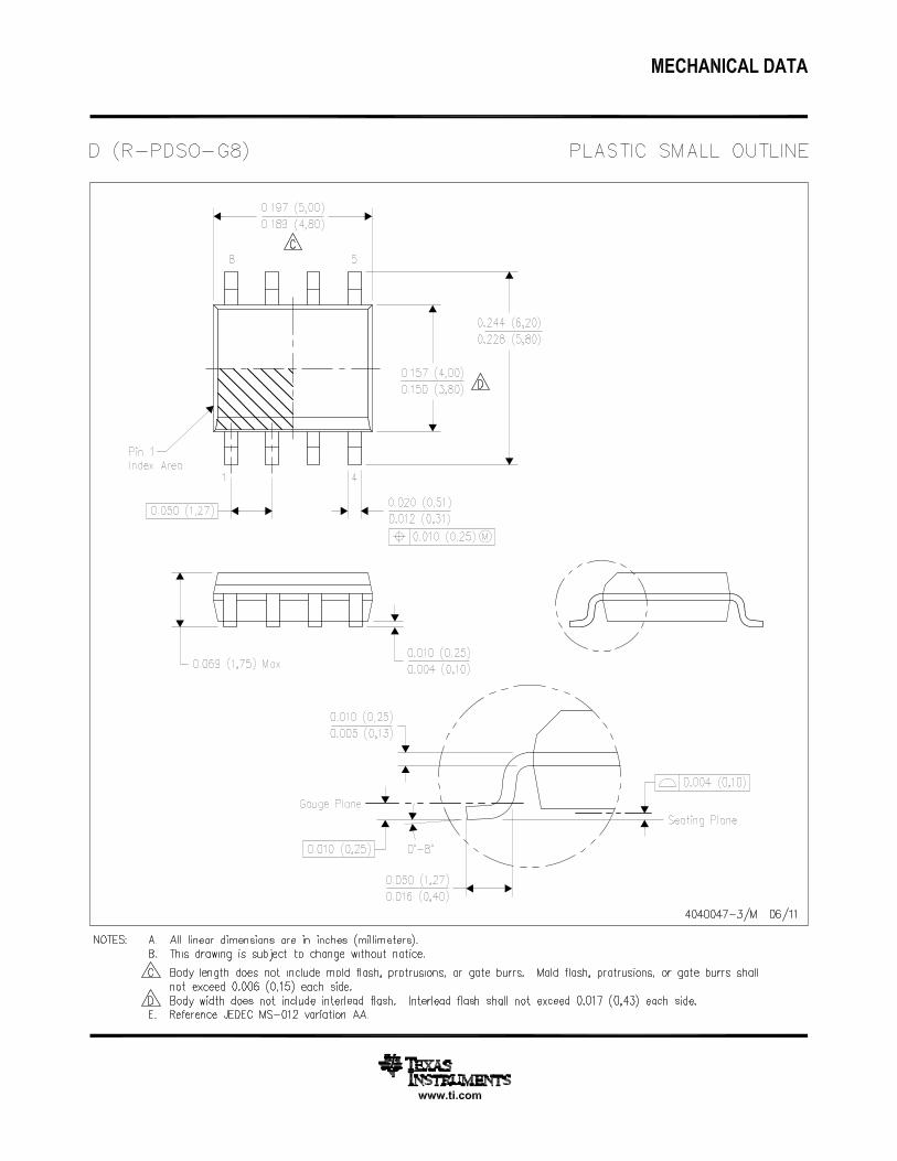
Figure 1. VSSOP, Small Outline, and PDIP Figure 2. WSON Package (Top View)Package See Package Number NGN0008ATop View
See Package Number DGK0008A, D0008A, orD0008E
1
Please be aware that an important notice concerning availability, standard warranty, and use in critical applications ofTexas Instruments semiconductor products and disclaimers thereto appears at the end of this data sheet.
2All trademarks are the property of their respective owners.
PRODUCTION DATA information is current as of publication date. Copyright © 2000–2013, Texas Instruments IncorporatedProducts conform to specifications per the terms of the TexasInstruments standard warranty. Production processing does notnecessarily include testing of all parameters.
LM4871
SNAS002F –FEBRUARY 2000–REVISED MAY 2013 www.ti.com
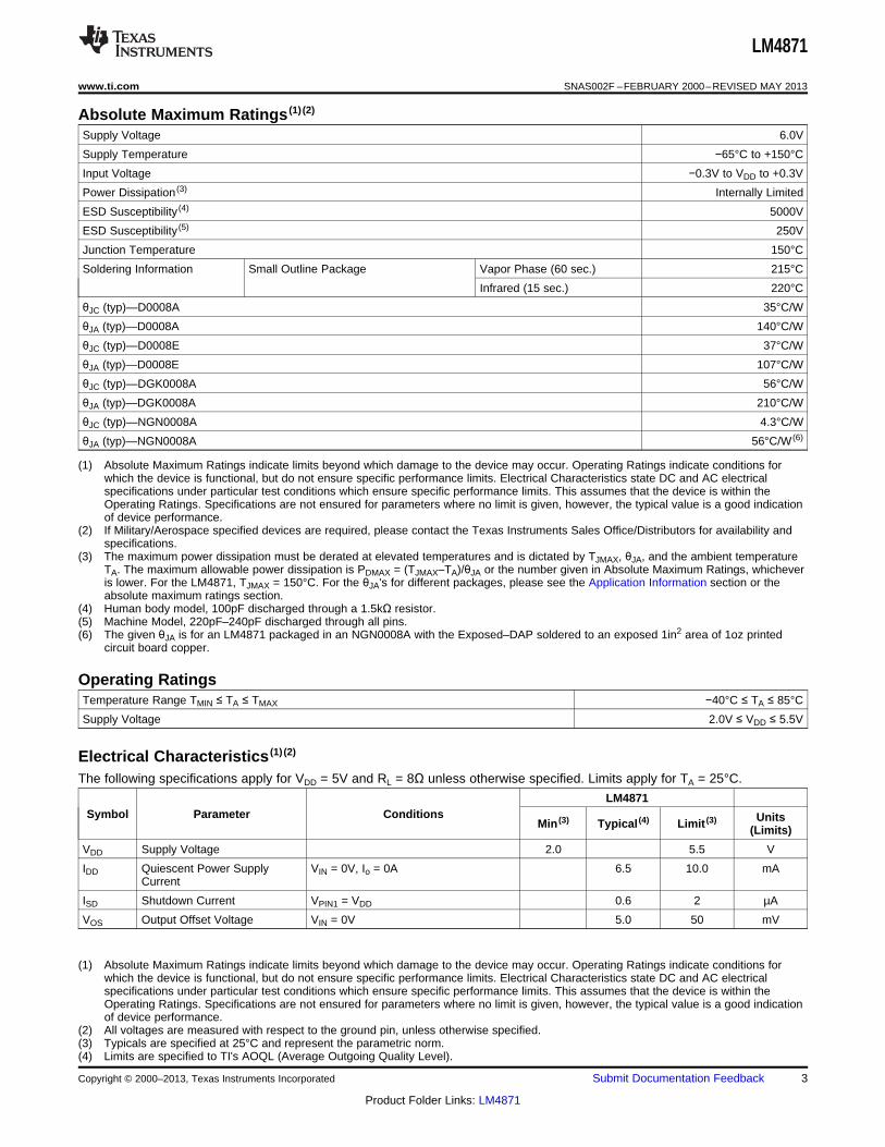
Typical Application
Figure 3. Typical Audio Amplifier Application Circuit
These devices have limited built-in ESD protection. The leads should be shorted together or the device placed in conductive foamduring storage or handling to prevent electrostatic damage to the MOS gates.
2 Submit Documentation Feedback Copyright © 2000–2013, Texas Instruments Incorporated
Product Folder Links: LM4871
LM4871
www.ti.com SNAS002F –FEBRUARY 2000–REVISED MAY 2013
Absolute Maximum Ratings (1) (2)
Supply Voltage 6.0V
Supply Temperature −65°C to +150°C
Input Voltage −0.3V to VDD to +0.3V
Power Dissipation (3) Internally Limited
ESD Susceptibility (4) 5000V
ESD Susceptibility (5) 250V
Junction Temperature 150°C
Soldering Information Small Outline Package Vapor Phase (60 sec.) 215°C
Infrared (15 sec.) 220°C
θJC (typ)—D0008A 35°C/W
θJA (typ)—D0008A 140°C/W
θJC (typ)—D0008E 37°C/W
θJA (typ)—D0008E 107°C/W
θJC (typ)—DGK0008A 56°C/W
θJA (typ)—DGK0008A 210°C/W
θJC (typ)—NGN0008A 4.3°C/W
θJA (typ)—NGN0008A 56°C/W (6)
(1) Absolute Maximum Ratings indicate limits beyond which damage to the device may occur. Operating Ratings indicate conditions forwhich the device is functional, but do not ensure specific performance limits. Electrical Characteristics state DC and AC electricalspecifications under particular test conditions which ensure specific performance limits. This assumes that the device is within theOperating Ratings. Specifications are not ensured for parameters where no limit is given, however, the typical value is a good indicationof device performance.
(2) If Military/Aerospace specified devices are required, please contact the Texas Instruments Sales Office/Distributors for availability andspecifications.
(3) The maximum power dissipation must be derated at elevated temperatures and is dictated by TJMAX, θJA, and the ambient temperatureTA. The maximum allowable power dissipation is PDMAX = (TJMAX–TA)/θJA or the number given in Absolute Maximum Ratings, whicheveris lower. For the LM4871, TJMAX = 150°C. For the θJA's for different packages, please see the Application Information section or theabsolute maximum ratings section.
(4) Human body model, 100pF discharged through a 1.5kΩ resistor.(5) Machine Model, 220pF–240pF discharged through all pins.(6) The given θJA is for an LM4871 packaged in an NGN0008A with the Exposed–DAP soldered to an exposed 1in2 area of 1oz printed
circuit board copper.
Operating RatingsTemperature Range TMIN ≤ TA ≤ TMAX −40°C ≤ TA ≤ 85°C
Supply Voltage 2.0V ≤ VDD ≤ 5.5V
Electrical Characteristics (1) (2)
The following specifications apply for VDD = 5V and RL = 8Ω unless otherwise specified. Limits apply for TA = 25°C.
LM4871Symbol Parameter Conditions UnitsMin (3) Typical (4) Limit (3)
(Limits)
VDD Supply Voltage 2.0 5.5 V
IDD Quiescent Power Supply VIN = 0V, Io = 0A 6.5 10.0 mACurrent
ISD Shutdown Current VPIN1 = VDD 0.6 2 µA
VOS Output Offset Voltage VIN = 0V 5.0 50 mV
(1) Absolute Maximum Ratings indicate limits beyond which damage to the device may occur. Operating Ratings indicate conditions forwhich the device is functional, but do not ensure specific performance limits. Electrical Characteristics state DC and AC electricalspecifications under particular test conditions which ensure specific performance limits. This assumes that the device is within theOperating Ratings. Specifications are not ensured for parameters where no limit is given, however, the typical value is a good indicationof device performance.
(2) All voltages are measured with respect to the ground pin, unless otherwise specified.(3) Typicals are specified at 25°C and represent the parametric norm.(4) Limits are specified to TI's AOQL (Average Outgoing Quality Level).
Copyright © 2000–2013, Texas Instruments Incorporated Submit Documentation Feedback 3
Product Folder Links: LM4871
LM4871
SNAS002F –FEBRUARY 2000–REVISED MAY 2013 www.ti.com
Electrical Characteristics(1)(2) (continued)The following specifications apply for VDD = 5V and RL = 8Ω unless otherwise specified. Limits apply for TA = 25°C.
LM4871Symbol Parameter Conditions UnitsMin (3) Typical (4) Limit (3)
(Limits)
Po Output Power THD = 1%, f = 1kHz
LM4871LD, RL = 3Ω (5) 2.38 WLM4871LD, RL = 4Ω (5) 2LM4871, RL = 8Ω (5) 1.2
THD+N = 10%, f = 1kHzLM4871LD, RL = 3Ω (5) 3 WLM4871LD, RL = 4Ω (5) 2.5LM4871, RL = 8Ω (5) 1.5
THD+N Total Harmonic 20Hz ≤ f ≤ 20kHz, AVD = 2Distortion+Noise LM4871LD, RL = 4Ω, P O = 1.6W 0.13 %
LM4871, RL = 8Ω, P O = 1W 0.25
PSRR Power Supply Rejection Ratio VDD = 4.9V to 5.1V 60 dB
(5) When driving 3Ω or 4Ω loads from a 5V supply, the LM4871LD must be mounted to a circuit board.
External Components Description(Figure 3)
Components Functional Description
1. Ri Inverting input resistance that sets the closed-loop gain in conjunction with Rf. This resistor also forms a high pass filterwith Ci at fC= 1/(2π RiCi).
2. Ci Input coupling capacitor that blocks the DC voltage at the amplifiers input terminals. Also creates a highpass filter withRi at fc = 1/(2π RiCi). Refer to the section, Proper Selection of External Components, for an explanation of how todetermine the value of Ci.
3. Rf Feedback resistance that sets the closed-loop gain in conjunction with Ri.
4. CS Supply bypass capacitor that provides power supply filtering. Refer to the Power Supply Bypassing section forinformation concerning proper placement and selection of the supply bypass capacitor.
5. CB Bypass pin capacitor that provides half-supply filtering. Refer to the section, Proper Selection of External Components,for information concerning proper placement and selection of CB.
4 Submit Documentation Feedback Copyright © 2000–2013, Texas Instruments Incorporated
Product Folder Links: LM4871
LM4871
www.ti.com SNAS002F –FEBRUARY 2000–REVISED MAY 2013
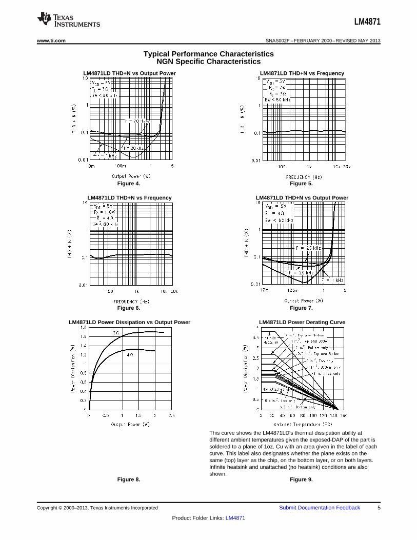
Typical Performance CharacteristicsNGN Specific Characteristics
LM4871LD THD+N vs Output Power LM4871LD THD+N vs Frequency
Figure 4. Figure 5.
LM4871LD THD+N vs Frequency LM4871LD THD+N vs Output Power
Figure 6. Figure 7.
LM4871LD Power Dissipation vs Output Power LM4871LD Power Derating Curve
This curve shows the LM4871LD's thermal dissipation ability atdifferent ambient temperatures given the exposed-DAP of the part issoldered to a plane of 1oz. Cu with an area given in the label of eachcurve. This label also designates whether the plane exists on thesame (top) layer as the chip, on the bottom layer, or on both layers.Infinite heatsink and unattached (no heatsink) conditions are alsoshown.
Figure 8. Figure 9.
Copyright © 2000–2013, Texas Instruments Incorporated Submit Documentation Feedback 5
Product Folder Links: LM4871
LM4871
SNAS002F –FEBRUARY 2000–REVISED MAY 2013 www.ti.com
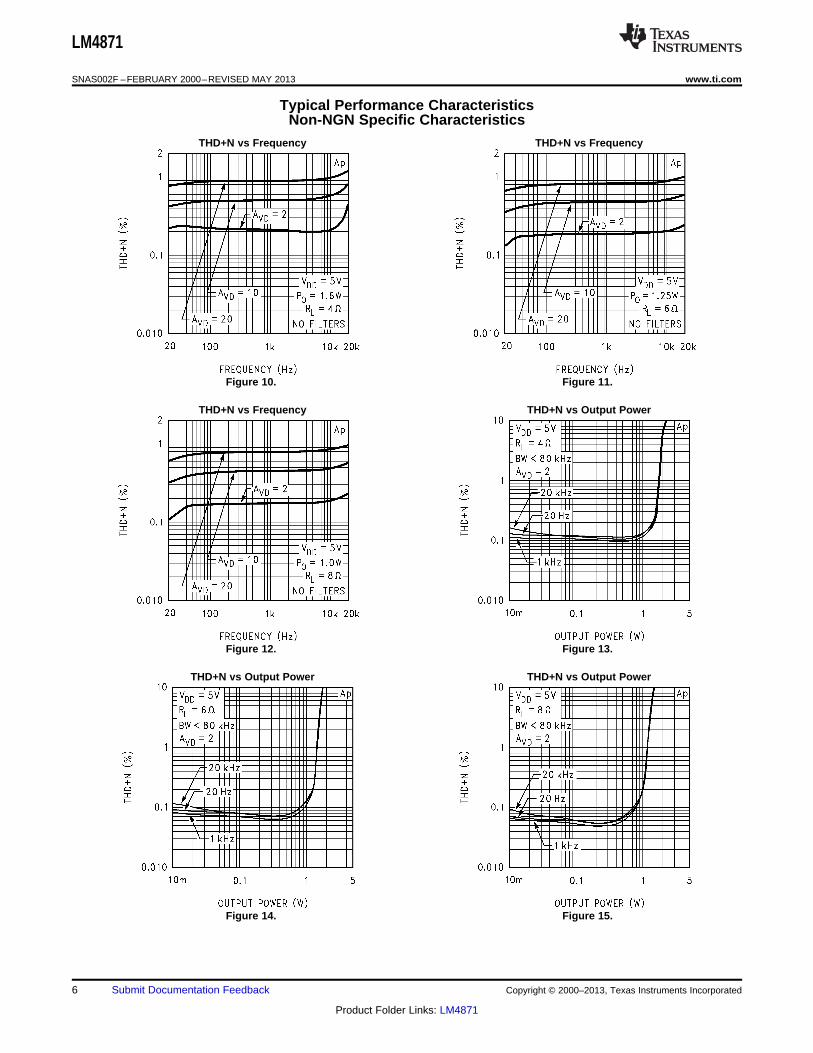
Typical Performance CharacteristicsNon-NGN Specific Characteristics
THD+N vs Frequency THD+N vs Frequency
Figure 10. Figure 11.
THD+N vs Frequency THD+N vs Output Power
Figure 12. Figure 13.
THD+N vs Output Power THD+N vs Output Power
Figure 14. Figure 15.
6 Submit Documentation Feedback Copyright © 2000–2013, Texas Instruments Incorporated
Product Folder Links: LM4871
LM4871
www.ti.com SNAS002F –FEBRUARY 2000–REVISED MAY 2013
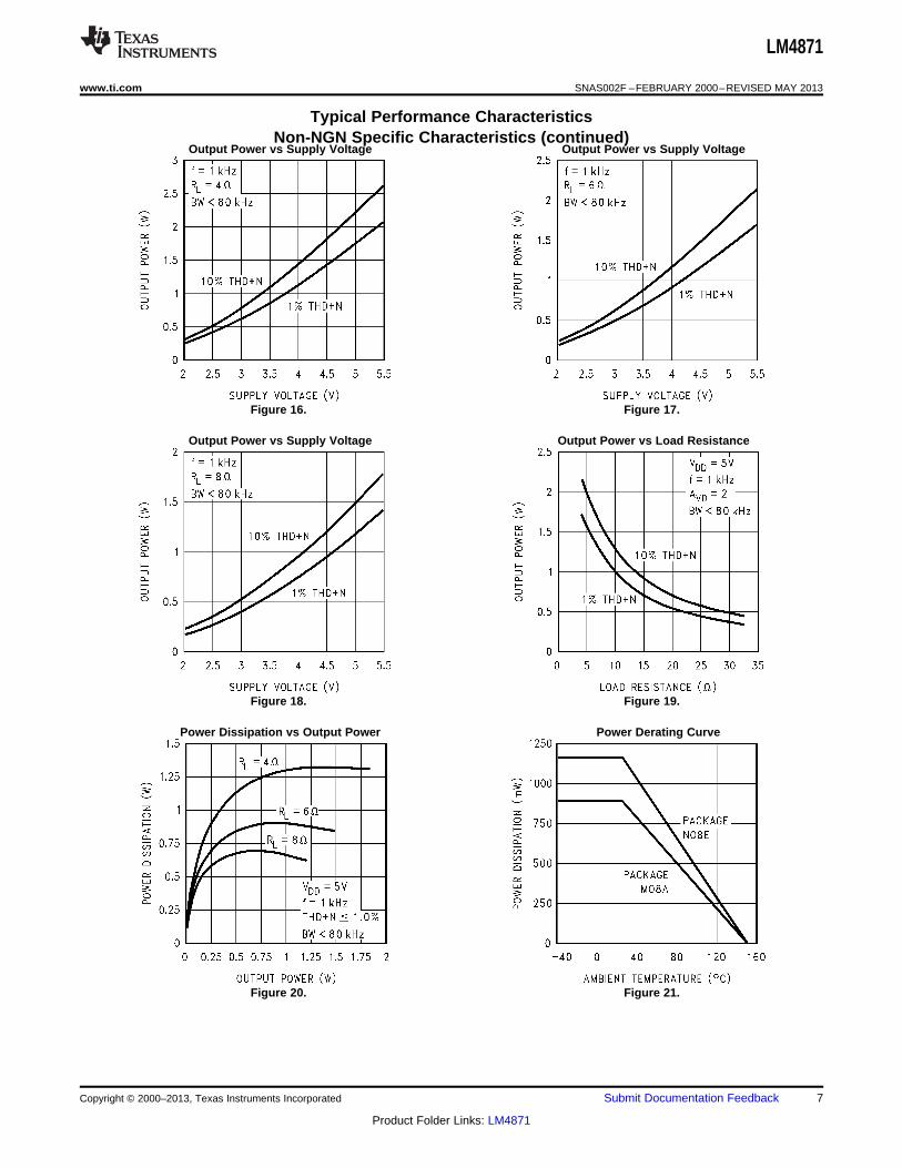
Typical Performance CharacteristicsNon-NGN Specific Characteristics (continued)
Output Power vs Supply Voltage Output Power vs Supply Voltage
Figure 16. Figure 17.
Output Power vs Supply Voltage Output Power vs Load Resistance
Figure 18. Figure 19.
Power Dissipation vs Output Power Power Derating Curve
Figure 20. Figure 21.
Copyright © 2000–2013, Texas Instruments Incorporated Submit Documentation Feedback 7
Product Folder Links: LM4871
LM4871
SNAS002F –FEBRUARY 2000–REVISED MAY 2013 www.ti.com
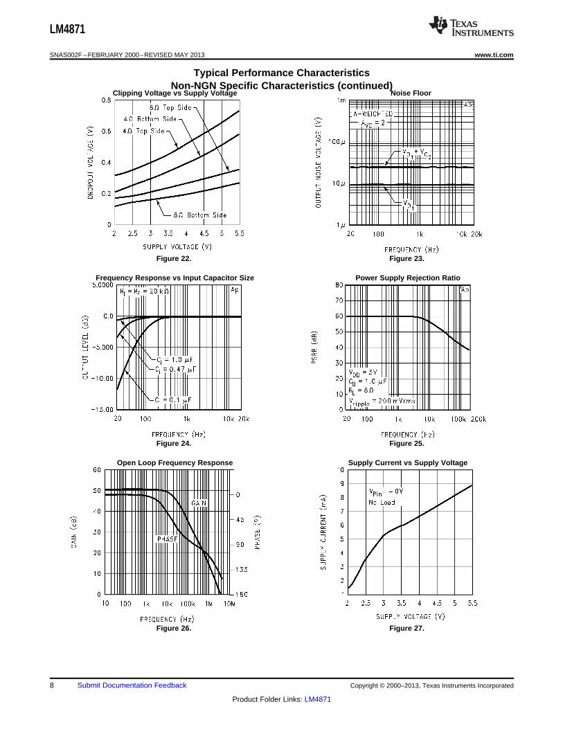
Typical Performance CharacteristicsNon-NGN Specific Characteristics (continued)
Clipping Voltage vs Supply Voltage Noise Floor
Figure 22. Figure 23.
Frequency Response vs Input Capacitor Size Power Supply Rejection Ratio
Figure 24. Figure 25.
Open Loop Frequency Response Supply Current vs Supply Voltage
Figure 26. Figure 27.
8 Submit Documentation Feedback Copyright © 2000–2013, Texas Instruments Incorporated
Product Folder Links: LM4871
LM4871
www.ti.com SNAS002F –FEBRUARY 2000–REVISED MAY 2013
APPLICATION INFORMATION
EXPOSED-DAP PACKAGE PCB MOUNTING CONSIDERATION
The LM4871's exposed-DAP (die attach paddle) package (NGN) provides a low thermal resistance between thedie and the PCB to which the part is mounted and soldered. This allows rapid heat transfer from the die to thesurrounding PCB copper traces, ground plane, and surrounding air. The result is a low voltage audio poweramplifier that produces 2W at ≤ 1% THD with a 4Ω load. This high power is achieved through carefulconsideration of necessary thermal design. Failing to optimize thermal design may compromise the LM4871'shigh power performance and activate unwanted, though necessary, thermal shutdown protection.
The NGN package must have its DAP soldered to a copper pad on the PCB. The DAP's PCB copper pad isconnected to a large plane of continuous unbroken copper. This plane forms a thermal mass, heat sink, andradiation area. Place the heat sink area on either outside plane in the case of a two-sided PCB, or on an innerlayer of a board with more than two layers. Connect the DAP copper pad to the inner layer or backside copperheat sink area with 4(2x2) vias. The via diameter should be 0.012in-0.013in with a 1.27mm pitch. Ensure efficientthermal conductivity by plating through the vias.
Best thermal performance is achieved with the largest practical heat sink area. If the heatsink and amplifier sharethe same PCB layer, a nominal 2.5in2 area is necessary for 5V operation with a 4Ω load. Heatsink areas notplaced on the same PCB layer as the LM4871 should be 5in2 (min) for the same supply voltage and loadresistance. The last two area recommendations apply for 25°C ambient temperature. Increase the area tocompensate for ambient temperatures above 25°C. The LM4871's power de-rating curve in the TypicalPerformance Characteristics shows the maximum power dissipation versus temperature. An example PCB layoutfor the NGN package is shown in the Demonstration Board Layout section. Further detailed and specificinformation concerning PCB layout, fabrication, and mounting an NGN (WSON) package is available from TI'sPackage Engineering Group under application note AN-1187 (Literature Number SNOA401).
PCB LAYOUT AND SUPPLY REGULATION CONSIDERATIONS FOR DRIVING 3Ω AND 4ΩLOADS
Power dissipated by a load is a function of the voltage swing across the load and the load's impedance. As loadimpedance decreases, load dissipation becomes increasingly dependant on the interconnect (PCB trace andwire) resistance between the amplifier output pins and the load's connections. Residual trace resistance causesa voltage drop, which results in power dissipated in the trace and not in the load as desired. For example, 0.1Ωtrace resistance reduces the output power dissipated by a 4Ω load from 2.0W to 1.95W. This problem ofdecreased load dissipation is exacerbated as load impedance decreases. Therefore, to maintain the highest loaddissipation and widest output voltage swing, PCB traces that connect the output pins to a load must be as wideas possible.
Poor power supply regulation adversely affects maximum output power. A poorly regulated supply's outputvoltage decreases with increasing load current. Reduced supply voltage causes decreased headroom, outputsignal clipping, and reduced output power. Even with tightly regulated supplies, trace resistance creates thesame effects as poor supply regulation. Therefore, making the power supply traces as wide as possible helpsmaintain full output voltage swing.
BRIDGE CONFIGURATION EXPLANATION
As shown in Figure 3, the LM4871 has two operational amplifiers internally, allowing for a few different amplifierconfigurations. The first amplifier's gain is externally configurable; the second amplifier is internally fixed in aunity-gain, inverting configuration. The closed-loop gain of the first amplifier is set by selecting the ratio of Rf to Riwhile the second amplifier's gain is fixed by the two internal 40kΩ resistors. Figure 3 shows that the output ofamplifier one serves as the input to amplifier two, which results in both amplifiers producing signals identical inmagnitude, but 180° out of phase. Consequently, the differential gain for the IC is
AVD= 2 *(Rf/Ri) (1)
By driving the load differentially through outputs Vo1 and Vo2, an amplifier configuration commonly referred to as“bridged mode” is established. Bridged mode operation is different from the classical single-ended amplifierconfiguration where one side of its load is connected to ground.
Copyright © 2000–2013, Texas Instruments Incorporated Submit Documentation Feedback 9
Product Folder Links: LM4871
LM4871
SNAS002F –FEBRUARY 2000–REVISED MAY 2013 www.ti.com
A bridge amplifier design has a few distinct advantages over the single-ended configuration, as it providesdifferential drive to the load, thus doubling output swing for a specified supply voltage. Four times the outputpower is possible as compared to a single-ended amplifier under the same conditions. This increase in attainableoutput power assumes that the amplifier is not current limited or clipped. In order to choose an amplifier's closed-loop gain without causing excessive clipping, please refer to the Audio Power Amplifier Design section.
Another advantage of the differential bridge output is no net DC voltage across load. This results from biasingVO1 and VO2 at the same DC voltage, in this case VDD/2 . This eliminates the coupling capacitor that singlesupply, single-ended amplifiers require. Eliminating an output coupling capacitor in a single-ended configurationforces a single supply amplifier's half-supply bias voltage across the load. The current flow created by the half-supply bias voltage increases internal IC power dissipation and my permanently damage loads such asspeakers.
POWER DISSIPATION
Power dissipation is a major concern when designing a successful amplifier, whether the amplifier is bridged orsingle-ended. A direct consequence of the increased power delivered to the load by a bridge amplifier is anincrease in internal power dissipation. Equation 2 states the maximum power dissipation point for a bridgeamplifier operating at a given supply voltage and driving a specified output load.
PDMAX = 4*(VDD)2/(2π2RL) (2)
Since the LM4871 has two operational amplifiers in one package, the maximum internal power dissipation is 4times that of a single-ended ampifier. Even with this substantial increase in power dissipation, the LM4871 doesnot require heatsinking under most operating conditions and output loading. From Equation 2, assuming a 5Vpower supply and an 8Ω load, the maximum power dissipation point is 625 mW. The maximum power dissipationpoint obtained from Equation 2 must not be greater than the power dissipation that results from Equation 3:
PDMAX = (TJMAX–TA)/θJA (3)
For the SOIC package, θJA = 140°C/W, for the PDIP package, θJA = 107°C/W, and for the VSSOP package, θJA= 210°C/W assuming free air operation. For the NGN package soldered to a DAP pad that expands to a copperarea of 1.0in2 on a PCB, the LM4871's θJA is 56°C/W. TJMAX = 150°C for the LM4871. The θJA can be decreasedby using some form of heat sinking. The resultant θJA will be the summation of the θJC, θCS, and θSA. θJC is thejunction to case of the package (or to the exposed DAP, as is the case with the NGN package), θCS is the caseto heat sink thermal resistance and θSA is the heat sink to ambient thermal resistance. By adding additionalcopper area around the LM4871, the θJA can be reduced from its free air value for the SOIC and VSSOPpackages. Increasing the copper area around the NGN package from 1.0in2 to 2.0in2 area results in a θJAdecrease to 46°C/W. Depending on the ambient temperature, TA, and the θJA, Equation 3 can be used to find themaximum internal power dissipation supported by the IC packaging. If the result of Equation 2 is greater thanthat of Equation 3, then either the supply voltage must be decreased, the load impedance increased, the θJAdecreased, or the ambient temperature reduced. For the typical application of a 5V power supply, with an 8Ωload, and no additional heatsinking, the maximum ambient temperature possible without violating the maximumjunction temperature is approximately 61°C provided that device operation is around the maximum powerdissipation point and assuming surface mount packaging. For the NGN package in a typical application of a 5Vpower supply, with a 4Ω load, and 1.0in2 copper area soldered to the exposed DAP pad, the maximum ambienttemperature is approximately 77°C providing device operation is around the maximum power dissipation point.Internal power dissipation is a function of output power. If typical operation is not around the maximum powerdissipation point, the ambient temperature can be increased. Refer to the Typical Performance Characteristicscurves for power dissipation information for different output powers and output loading.
POWER SUPPLY BYPASSING
As with any amplifier, proper supply bypassing is critical for low noise performance and high power supplyrejection. The capacitor location on both the bypass and power supply pins should be as close to the LM4871 aspossible. The capacitor connected between the bypass pin and ground improves the internal bias voltage'sstability, producing improved PSRR. The improvements to PSRR increase as the bypass pin capacitor increases.Typical applications employ a 5V regulator with 10µF and a 0.1µF bypass capacitors which aid in supply stability.This does not eliminate the need for bypassing the supply nodes of the LM4871 with a 1µF tantalum capacitor.The selection of bypass capacitors, especially CB, is dependent upon PSRR requirements, click and popperformance as explained in the section, Proper Selection of External Components, system cost, and sizeconstraints.
10 Submit Documentation Feedback Copyright © 2000–2013, Texas Instruments Incorporated
Product Folder Links: LM4871
LM4871
www.ti.com SNAS002F –FEBRUARY 2000–REVISED MAY 2013
SHUTDOWN FUNCTION
In order to reduce power consumption while not in use, the LM4871 contains a shutdown pin to externally turn offthe amplifier's bias circuitry. This shutdown feature turns the amplifier off when a logic high is placed on theshutdown pin. The trigger point between a logic low and logic high level is typically half- supply. It is best toswitch between ground and supply to provide maximum device performance. By switching the shutdown pin toVDD, the LM4871 supply current draw will be minimized in idle mode. While the device will be disabled withshutdown pin voltages less then VDD, the idle current may be greater than the typical value of 0.6µA. In eithercase, the shutdown pin should be tied to a definite voltage to avoid unwanted state changes.
In many applications, a microcontroller or microprocessor output is used to control the shutdown circuitry whichprovides a quick, smooth transition into shutdown. Another solution is to use a single-pole, single-throw switch inconjunction with an external pull-up resistor. When the switch is closed, the shutdown pin is connected to groundand enables the amplifier. If the switch is open, then the external pull-up resistor will disable the LM4871. Thisscheme ensures that the shutdown pin will not float thus preventing unwanted state changes.
PROPER SELECTION OF EXTERNAL COMPONENTS
Proper selection of external components in applications using integrated power amplifiers is critical to optimizedevice and system performance. While the LM4871 is tolerant of external component combinations,consideration to component values must be used to maximize overall system quality.
The LM4871 is unity-gain stable which gives a designer maximum system flexibility. The LM4871 should be usedin low gain configurations to minimize THD+N values, and maximize the signal to noise ratio. Low gainconfigurations require large input signals to obtain a given output power. Input signals equal to or greater than 1Vrms are available from sources such as audio codecs. Please refer to the section, Audio Power AmplifierDesign, for a more complete explanation of proper gain selection.
Besides gain, one of the major considerations is the closed-loop bandwidth of the amplifier. To a large extent, thebandwidth is dictated by the choice of external components shown in Audio Power Amplifier Design. The inputcoupling capacitor, Ci, forms a first order high pass filter which limits low frequency response. This value shouldbe chosen based on needed frequency response for a few distinct reasons.
Selection Of Input Capacitor Size
Large input capacitors are both expensive and space hungry for portable designs. Clearly, a certain sizedcapacitor is needed to couple in low frequencies without severe attenuation. But in many cases the speakersused in portable systems, whether internal or external, have little ability to reproduce signals below 100Hz to150Hz. Thus, using a large input capacitor may not increase actual system performance.
In addition to system cost and size, click and pop performance is effected by the size of the input couplingcapacitor, Ci. A larger input coupling capacitor requires more charge to reach its quiescent DC voltage (nominally1/2 VDD). This charge comes from the output via the feedback and is apt to create pops upon device enable.Thus, by minimizing the capacitor size based on necessary low frequency response, turn-on pops can beminimized.
Besides minimizing the input capacitor size, careful consideration should be paid to the bypass capacitor value.Bypass capacitor, CB, is the most critical component to minimize turn-on pops since it determines how fast theLM4871 turns on. The slower the LM4871's outputs ramp to their quiescent DC voltage (nominally 1/2 VDD), thesmaller the turn-on pop. Choosing CB equal to 1.0µF along with a small value of Ci (in the range of 0.1µF to0.39µF), should produce a virtually clickless and popless shutdown function. While the device will functionproperly, (no oscillations or motorboating), with CB equal to 0.1µF, the device will be much more susceptible toturn-on clicks and pops. Thus, a value of CB equal to 1.0µF is recommended in all but the most cost sensitivedesigns.
Copyright © 2000–2013, Texas Instruments Incorporated Submit Documentation Feedback 11
Product Folder Links: LM4871
LM4871
SNAS002F –FEBRUARY 2000–REVISED MAY 2013 www.ti.com
AUDIO POWER AMPLIFIER DESIGN
Design a 1W/8Ω Audio Amplifier
Given:
Power Output 1 Wrms
Load Impedance 8ΩInput Level 1 Vrms
Input Impedance 20 kΩBandwidth 100 Hz–20 kHz ± 0.25 dB
A designer must first determine the minimum supply rail to obtain the specified output power. By extrapolatingfrom the Output Power vs Supply Voltage graphs in the Typical Performance Characteristics section, the supplyrail can be easily found. A second way to determine the minimum supply rail is to calculate the required Vopeakusing Equation 4 and add the output voltage. Using this method, the minimum supply voltage would be (Vopeak +(VODTOP + VODBOT)), where VODBOT and VODTOP are extrapolated from the Dropout Voltage vs Supply Voltage curve inthe Typical Performance Characteristics section.
(4)
Using the Output Power vs Supply Voltage graph for an 8Ω load, the minimum supply rail is 4.6V. But since 5V isa standard voltage in most applications, it is chosen for the supply rail. Extra supply voltage creates headroomthat allows the LM4871 to reproduce peaks in excess of 1W without producing audible distortion. At this time, thedesigner must make sure that the power supply choice along with the output impedance does not violate theconditions explained in the POWER DISSIPATION section.
Once the power dissipation equations have been addressed, the required differential gain can be determinedfrom Equation 5.
(5)Rf/Ri = AVD/2 (6)
From Equation 5, the minimum AVD is 2.83; use AVD = 3.
Since the desired input impedance was 20kΩ, and with a AVD impedance of 2, a ratio of 1.5:1 of Rf to Ri resultsin an allocation of Ri = 20kΩ and Rf = 30kΩ. The final design step is to address the bandwidth requirementswhich must be stated as a pair of −3dB frequency points. Five times away from a −3dB point is 0.17dB downfrom passband response which is better than the required ±0.25dB specified.
fL = 100Hz/5 = 20Hz
fH = 20kHz * 5 = 100kHz
As stated in the External Components Description section, Ri in conjunction with Ci create a highpass filter.
Ci ≥ 1/(2π*20kΩ*20Hz) = 0.397µF; use 0.39µF
The high frequency pole is determined by the product of the desired frequency pole, fH, and the differential gain,AVD. With a AVD = 3 and fH = 100kHz, the resulting GBWP = 150kHz which is much smaller than the LM4871GBWP of 4MHz. This figure displays that if a designer has a need to design an amplifier with a higher differentialgain, the LM4871 can still be used without running into bandwidth limitations.
12 Submit Documentation Feedback Copyright © 2000–2013, Texas Instruments Incorporated
Product Folder Links: LM4871
LM4871
www.ti.com SNAS002F –FEBRUARY 2000–REVISED MAY 2013
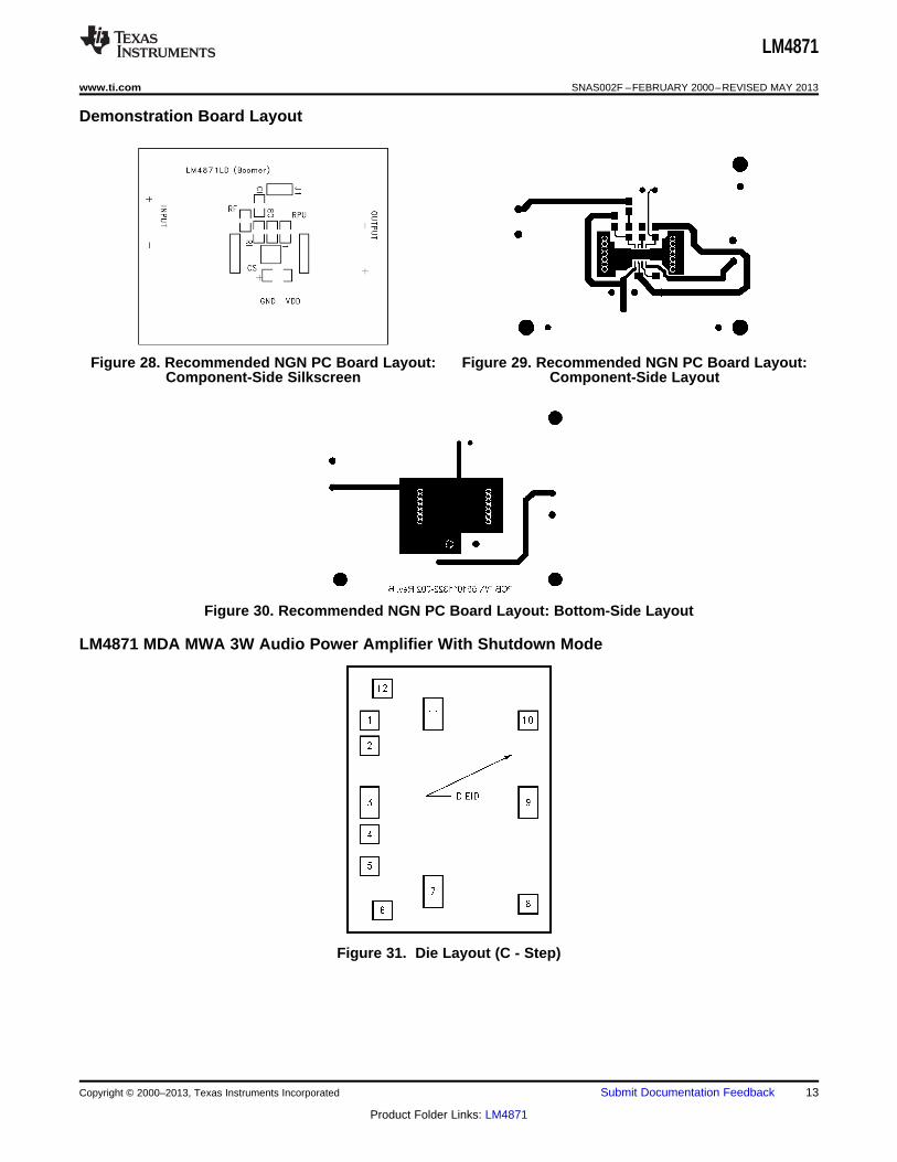
Demonstration Board Layout
Figure 28. Recommended NGN PC Board Layout: Figure 29. Recommended NGN PC Board Layout:Component-Side Silkscreen Component-Side Layout
Figure 30. Recommended NGN PC Board Layout: Bottom-Side Layout
LM4871 MDA MWA 3W Audio Power Amplifier With Shutdown Mode
Figure 31. Die Layout (C - Step)
Copyright © 2000–2013, Texas Instruments Incorporated Submit Documentation Feedback 13
Product Folder Links: LM4871
LM4871
SNAS002F –FEBRUARY 2000–REVISED MAY 2013 www.ti.com
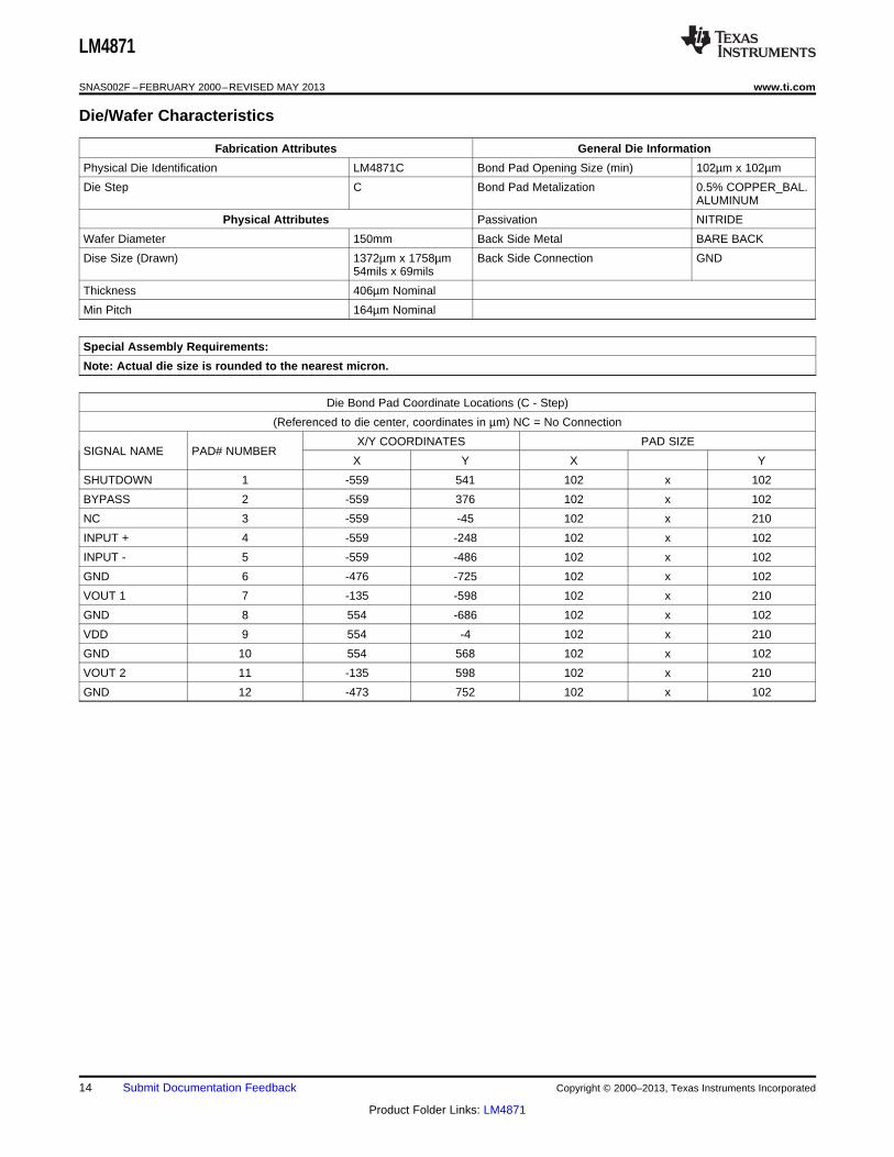
Die/Wafer Characteristics
Fabrication Attributes General Die Information
Physical Die Identification LM4871C Bond Pad Opening Size (min) 102µm x 102µm
Die Step C Bond Pad Metalization 0.5% COPPER_BAL.ALUMINUM
Physical Attributes Passivation NITRIDE
Wafer Diameter 150mm Back Side Metal BARE BACK
Dise Size (Drawn) 1372µm x 1758µm Back Side Connection GND54mils x 69mils
Thickness 406µm Nominal
Min Pitch 164µm Nominal
Special Assembly Requirements:
Note: Actual die size is rounded to the nearest micron.
Die Bond Pad Coordinate Locations (C - Step)
(Referenced to die center, coordinates in µm) NC = No Connection
X/Y COORDINATES PAD SIZESIGNAL NAME PAD# NUMBER
X Y X Y
SHUTDOWN 1 -559 541 102 x 102
BYPASS 2 -559 376 102 x 102
NC 3 -559 -45 102 x 210
INPUT + 4 -559 -248 102 x 102
INPUT - 5 -559 -486 102 x 102
GND 6 -476 -725 102 x 102
VOUT 1 7 -135 -598 102 x 210
GND 8 554 -686 102 x 102
VDD 9 554 -4 102 x 210
GND 10 554 568 102 x 102
VOUT 2 11 -135 598 102 x 210
GND 12 -473 752 102 x 102
14 Submit Documentation Feedback Copyright © 2000–2013, Texas Instruments Incorporated
Product Folder Links: LM4871
LM4871
www.ti.com SNAS002F –FEBRUARY 2000–REVISED MAY 2013
REVISION HISTORY
Changes from Revision E (May 2013) to Revision F Page
• Changed layout of National Data Sheet to TI format .......................................................................................................... 14
Copyright © 2000–2013, Texas Instruments Incorporated Submit Documentation Feedback 15
Product Folder Links: LM4871
PACKAGE OPTION ADDENDUM
www.ti.com 12-Jun-2014
Addendum-Page 1
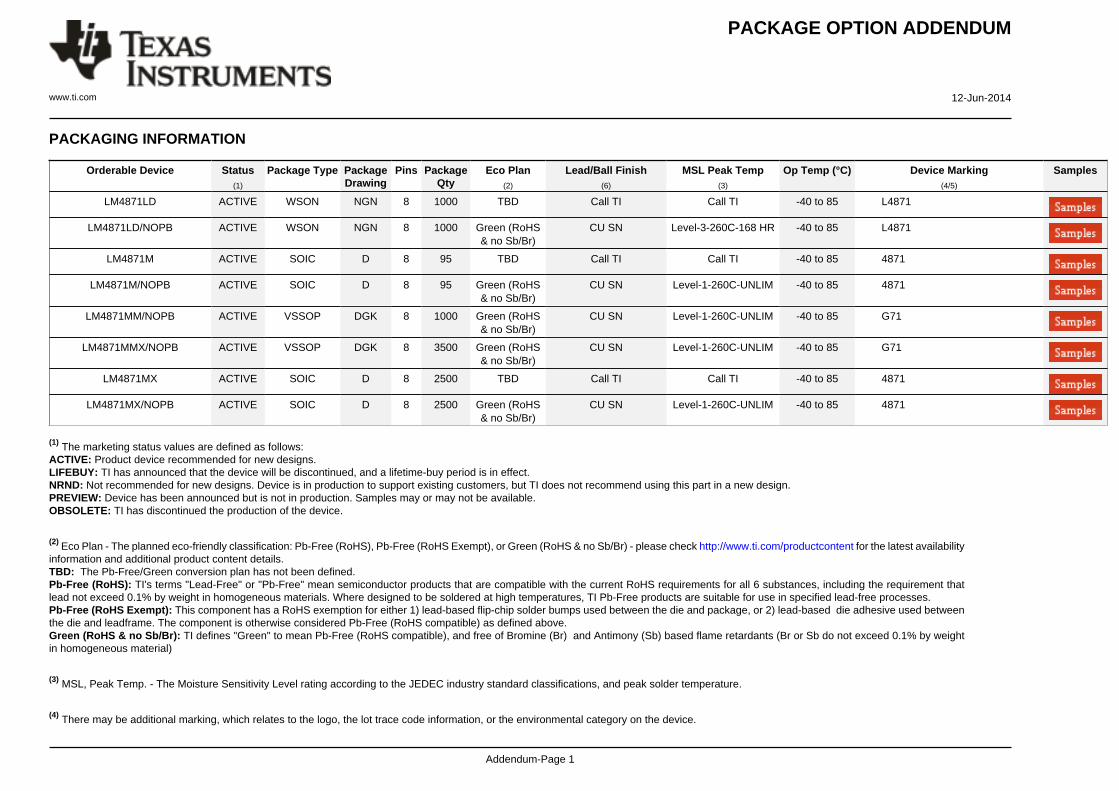
PACKAGING INFORMATION
Orderable Device Status(1)
Package Type PackageDrawing
Pins PackageQty
Eco Plan(2)
Lead/Ball Finish(6)
MSL Peak Temp(3)
Op Temp (°C) Device Marking(4/5)
Samples
LM4871LD ACTIVE WSON NGN 8 1000 TBD Call TI Call TI -40 to 85 L4871
LM4871LD/NOPB ACTIVE WSON NGN 8 1000 Green (RoHS& no Sb/Br)
CU SN Level-3-260C-168 HR -40 to 85 L4871
LM4871M ACTIVE SOIC D 8 95 TBD Call TI Call TI -40 to 85 4871
LM4871M/NOPB ACTIVE SOIC D 8 95 Green (RoHS& no Sb/Br)
CU SN Level-1-260C-UNLIM -40 to 85 4871
LM4871MM/NOPB ACTIVE VSSOP DGK 8 1000 Green (RoHS& no Sb/Br)
CU SN Level-1-260C-UNLIM -40 to 85 G71
LM4871MMX/NOPB ACTIVE VSSOP DGK 8 3500 Green (RoHS& no Sb/Br)
CU SN Level-1-260C-UNLIM -40 to 85 G71
LM4871MX ACTIVE SOIC D 8 2500 TBD Call TI Call TI -40 to 85 4871
LM4871MX/NOPB ACTIVE SOIC D 8 2500 Green (RoHS& no Sb/Br)
CU SN Level-1-260C-UNLIM -40 to 85 4871
(1) The marketing status values are defined as follows:ACTIVE: Product device recommended for new designs.LIFEBUY: TI has announced that the device will be discontinued, and a lifetime-buy period is in effect.NRND: Not recommended for new designs. Device is in production to support existing customers, but TI does not recommend using this part in a new design.PREVIEW: Device has been announced but is not in production. Samples may or may not be available.OBSOLETE: TI has discontinued the production of the device.
(2) Eco Plan - The planned eco-friendly classification: Pb-Free (RoHS), Pb-Free (RoHS Exempt), or Green (RoHS & no Sb/Br) - please check http://www.ti.com/productcontent for the latest availabilityinformation and additional product content details.TBD: The Pb-Free/Green conversion plan has not been defined.Pb-Free (RoHS): TI's terms "Lead-Free" or "Pb-Free" mean semiconductor products that are compatible with the current RoHS requirements for all 6 substances, including the requirement thatlead not exceed 0.1% by weight in homogeneous materials. Where designed to be soldered at high temperatures, TI Pb-Free products are suitable for use in specified lead-free processes.Pb-Free (RoHS Exempt): This component has a RoHS exemption for either 1) lead-based flip-chip solder bumps used between the die and package, or 2) lead-based die adhesive used betweenthe die and leadframe. The component is otherwise considered Pb-Free (RoHS compatible) as defined above.Green (RoHS & no Sb/Br): TI defines "Green" to mean Pb-Free (RoHS compatible), and free of Bromine (Br) and Antimony (Sb) based flame retardants (Br or Sb do not exceed 0.1% by weightin homogeneous material)
(3) MSL, Peak Temp. - The Moisture Sensitivity Level rating according to the JEDEC industry standard classifications, and peak solder temperature.
(4) There may be additional marking, which relates to the logo, the lot trace code information, or the environmental category on the device.
PACKAGE OPTION ADDENDUM
www.ti.com 12-Jun-2014
Addendum-Page 2
(5) Multiple Device Markings will be inside parentheses. Only one Device Marking contained in parentheses and separated by a "~" will appear on a device. If a line is indented then it is a continuationof the previous line and the two combined represent the entire Device Marking for that device.
(6) Lead/Ball Finish - Orderable Devices may have multiple material finish options. Finish options are separated by a vertical ruled line. Lead/Ball Finish values may wrap to two lines if the finishvalue exceeds the maximum column width.
Important Information and Disclaimer:The information provided on this page represents TI's knowledge and belief as of the date that it is provided. TI bases its knowledge and belief on informationprovided by third parties, and makes no representation or warranty as to the accuracy of such information. Efforts are underway to better integrate information from third parties. TI has taken andcontinues to take reasonable steps to provide representative and accurate information but may not have conducted destructive testing or chemical analysis on incoming materials and chemicals.TI and TI suppliers consider certain information to be proprietary, and thus CAS numbers and other limited information may not be available for release.
In no event shall TI's liability arising out of such information exceed the total purchase price of the TI part(s) at issue in this document sold by TI to Customer on an annual basis.
TAPE AND REEL INFORMATION
*All dimensions are nominal
Device PackageType
PackageDrawing
Pins SPQ ReelDiameter
(mm)
ReelWidth
W1 (mm)
A0(mm)
B0(mm)
K0(mm)
P1(mm)
W(mm)
Pin1Quadrant
LM4871LD WSON NGN 8 1000 178.0 12.4 4.3 4.3 1.3 8.0 12.0 Q1
LM4871LD/NOPB WSON NGN 8 1000 178.0 12.4 4.3 4.3 1.3 8.0 12.0 Q1
LM4871MM/NOPB VSSOP DGK 8 1000 178.0 12.4 5.3 3.4 1.4 8.0 12.0 Q1
LM4871MMX/NOPB VSSOP DGK 8 3500 330.0 12.4 5.3 3.4 1.4 8.0 12.0 Q1
LM4871MX SOIC D 8 2500 330.0 12.4 6.5 5.4 2.0 8.0 12.0 Q1
LM4871MX/NOPB SOIC D 8 2500 330.0 12.4 6.5 5.4 2.0 8.0 12.0 Q1
PACKAGE MATERIALS INFORMATION
www.ti.com 20-Sep-2016
Pack Materials-Page 1
*All dimensions are nominal
Device Package Type Package Drawing Pins SPQ Length (mm) Width (mm) Height (mm)
LM4871LD WSON NGN 8 1000 210.0 185.0 35.0
LM4871LD/NOPB WSON NGN 8 1000 210.0 185.0 35.0
LM4871MM/NOPB VSSOP DGK 8 1000 210.0 185.0 35.0
LM4871MMX/NOPB VSSOP DGK 8 3500 367.0 367.0 35.0
LM4871MX SOIC D 8 2500 367.0 367.0 35.0
LM4871MX/NOPB SOIC D 8 2500 367.0 367.0 35.0
PACKAGE MATERIALS INFORMATION
www.ti.com 20-Sep-2016
Pack Materials-Page 2
MECHANICAL DATA
NGN0008A
www.ti.com
LDC08A (Rev B)
IMPORTANT NOTICE
Texas Instruments Incorporated and its subsidiaries (TI) reserve the right to make corrections, enhancements, improvements and otherchanges to its semiconductor products and services per JESD46, latest issue, and to discontinue any product or service per JESD48, latestissue. Buyers should obtain the latest relevant information before placing orders and should verify that such information is current andcomplete. All semiconductor products (also referred to herein as “components”) are sold subject to TI’s terms and conditions of salesupplied at the time of order acknowledgment.TI warrants performance of its components to the specifications applicable at the time of sale, in accordance with the warranty in TI’s termsand conditions of sale of semiconductor products. Testing and other quality control techniques are used to the extent TI deems necessaryto support this warranty. Except where mandated by applicable law, testing of all parameters of each component is not necessarilyperformed.TI assumes no liability for applications assistance or the design of Buyers’ products. Buyers are responsible for their products andapplications using TI components. To minimize the risks associated with Buyers’ products and applications, Buyers should provideadequate design and operating safeguards.TI does not warrant or represent that any license, either express or implied, is granted under any patent right, copyright, mask work right, orother intellectual property right relating to any combination, machine, or process in which TI components or services are used. Informationpublished by TI regarding third-party products or services does not constitute a license to use such products or services or a warranty orendorsement thereof. Use of such information may require a license from a third party under the patents or other intellectual property of thethird party, or a license from TI under the patents or other intellectual property of TI.Reproduction of significant portions of TI information in TI data books or data sheets is permissible only if reproduction is without alterationand is accompanied by all associated warranties, conditions, limitations, and notices. TI is not responsible or liable for such altereddocumentation. Information of third parties may be subject to additional restrictions.Resale of TI components or services with statements different from or beyond the parameters stated by TI for that component or servicevoids all express and any implied warranties for the associated TI component or service and is an unfair and deceptive business practice.TI is not responsible or liable for any such statements.Buyer acknowledges and agrees that it is solely responsible for compliance with all legal, regulatory and safety-related requirementsconcerning its products, and any use of TI components in its applications, notwithstanding any applications-related information or supportthat may be provided by TI. Buyer represents and agrees that it has all the necessary expertise to create and implement safeguards whichanticipate dangerous consequences of failures, monitor failures and their consequences, lessen the likelihood of failures that might causeharm and take appropriate remedial actions. Buyer will fully indemnify TI and its representatives against any damages arising out of the useof any TI components in safety-critical applications.In some cases, TI components may be promoted specifically to facilitate safety-related applications. With such components, TI’s goal is tohelp enable customers to design and create their own end-product solutions that meet applicable functional safety standards andrequirements. Nonetheless, such components are subject to these terms.No TI components are authorized for use in FDA Class III (or similar life-critical medical equipment) unless authorized officers of the partieshave executed a special agreement specifically governing such use.Only those TI components which TI has specifically designated as military grade or “enhanced plastic” are designed and intended for use inmilitary/aerospace applications or environments. Buyer acknowledges and agrees that any military or aerospace use of TI componentswhich have not been so designated is solely at the Buyer's risk, and that Buyer is solely responsible for compliance with all legal andregulatory requirements in connection with such use.TI has specifically designated certain components as meeting ISO/TS16949 requirements, mainly for automotive use. In any case of use ofnon-designated products, TI will not be responsible for any failure to meet ISO/TS16949.
Products ApplicationsAudio www.ti.com/audio Automotive and Transportation www.ti.com/automotiveAmplifiers amplifier.ti.com Communications and Telecom www.ti.com/communicationsData Converters dataconverter.ti.com Computers and Peripherals www.ti.com/computersDLP® Products www.dlp.com Consumer Electronics www.ti.com/consumer-appsDSP dsp.ti.com Energy and Lighting www.ti.com/energyClocks and Timers www.ti.com/clocks Industrial www.ti.com/industrialInterface interface.ti.com Medical www.ti.com/medicalLogic logic.ti.com Security www.ti.com/securityPower Mgmt power.ti.com Space, Avionics and Defense www.ti.com/space-avionics-defenseMicrocontrollers microcontroller.ti.com Video and Imaging www.ti.com/videoRFID www.ti-rfid.comOMAP Applications Processors www.ti.com/omap TI E2E Community e2e.ti.comWireless Connectivity www.ti.com/wirelessconnectivity
Mailing Address: Texas Instruments, Post Office Box 655303, Dallas, Texas 75265Copyright © 2016, Texas Instruments Incorporated