
LM 12 Datasheet
18
LM12,LM12CL LM12CL 80W Operational Amplifier Literature Number: SNOSBY8C
-
Upload
juan-sanchez-lopez -
Category
Documents
-
view
46 -
download
0
Transcript of LM 12 Datasheet
LM12,LM12CL
LM12CL 80W Operational Amplifier
Literature Number: SNOSBY8C
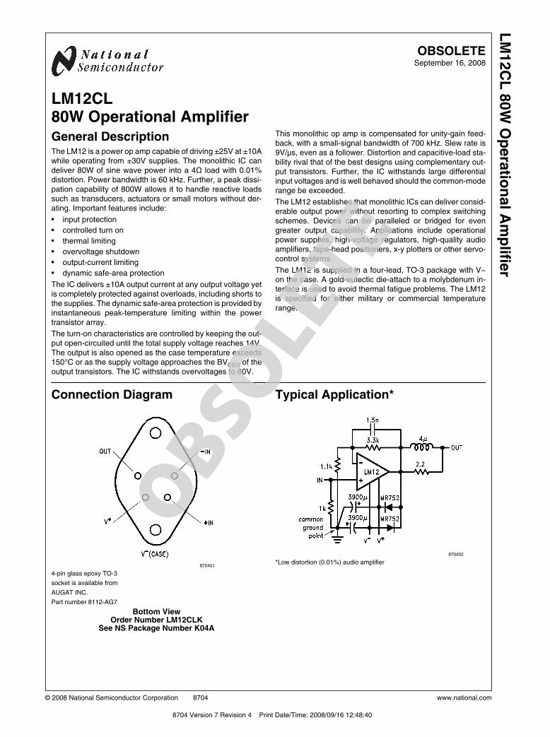
OBSOLETESeptember 16, 2008
LM12CL80W Operational AmplifierGeneral DescriptionThe LM12 is a power op amp capable of driving ±25V at ±10Awhile operating from ±30V supplies. The monolithic IC candeliver 80W of sine wave power into a 4Ω load with 0.01%distortion. Power bandwidth is 60 kHz. Further, a peak dissi-pation capability of 800W allows it to handle reactive loadssuch as transducers, actuators or small motors without der-ating. Important features include:
• input protection
• controlled turn on
• thermal limiting
• overvoltage shutdown
• output-current limiting
• dynamic safe-area protection
The IC delivers ±10A output current at any output voltage yetis completely protected against overloads, including shorts tothe supplies. The dynamic safe-area protection is provided byinstantaneous peak-temperature limiting within the powertransistor array.
The turn-on characteristics are controlled by keeping the out-put open-circuited until the total supply voltage reaches 14V.The output is also opened as the case temperature exceeds150°C or as the supply voltage approaches the BVCEO of theoutput transistors. The IC withstands overvoltages to 80V.
This monolithic op amp is compensated for unity-gain feed-back, with a small-signal bandwidth of 700 kHz. Slew rate is9V/μs, even as a follower. Distortion and capacitive-load sta-bility rival that of the best designs using complementary out-put transistors. Further, the IC withstands large differentialinput voltages and is well behaved should the common-moderange be exceeded.
The LM12 establishes that monolithic ICs can deliver consid-erable output power without resorting to complex switchingschemes. Devices can be paralleled or bridged for evengreater output capability. Applications include operationalpower supplies, high-voltage regulators, high-quality audioamplifiers, tape-head positioners, x-y plotters or other servo-control systems.
The LM12 is supplied in a four-lead, TO-3 package with V−on the case. A gold-eutectic die-attach to a molybdenum in-terface is used to avoid thermal fatigue problems. The LM12is specified for either military or commercial temperaturerange.
Connection Diagram
870401
4-pin glass epoxy TO-3
socket is available from
AUGAT INC.
Part number 8112-AG7
Bottom ViewOrder Number LM12CLK
See NS Package Number K04A
Typical Application*
870402
*Low distortion (0.01%) audio amplifier
© 2008 National Semiconductor Corporation 8704 www.national.com
8704 Version 7 Revision 4 Print Date/Time: 2008/09/16 12:48:40
LM
12C
L 8
0W
Op
era
tion
al A
mp
lifier
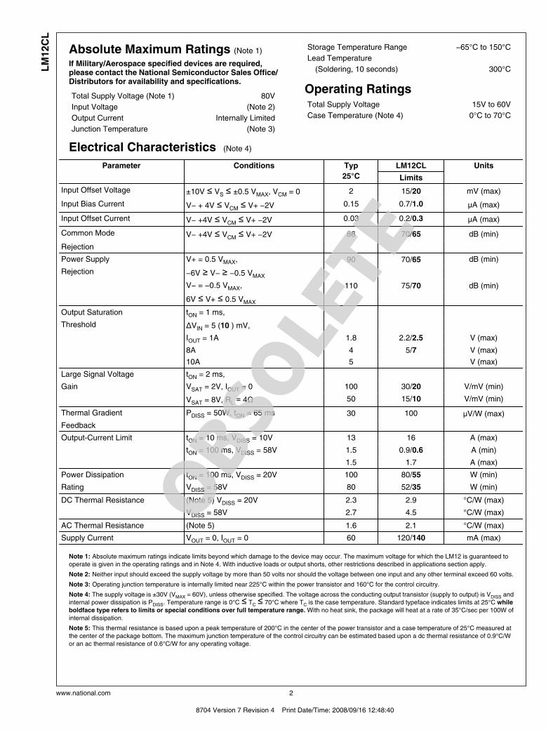
Absolute Maximum Ratings (Note 1)
If Military/Aerospace specified devices are required,please contact the National Semiconductor Sales Office/Distributors for availability and specifications.
Total Supply Voltage (Note 1) 80V
Input Voltage (Note 2)
Output Current Internally Limited
Junction Temperature (Note 3)
Storage Temperature Range −65°C to 150°C
Lead Temperature
(Soldering, 10 seconds) 300°C
Operating RatingsTotal Supply Voltage 15V to 60V
Case Temperature (Note 4) 0°C to 70°C
Electrical Characteristics (Note 4)
Parameter Conditions Typ
25°C
LM12CL Units
Limits
Input Offset Voltage ±10V ≤ VS ≤ ±0.5 VMAX, VCM = 0 2 15/20 mV (max)
Input Bias Current V− + 4V ≤ VCM ≤ V+ −2V 0.15 0.7/1.0 μA (max)
Input Offset Current V− +4V ≤ VCM ≤ V+ −2V 0.03 0.2/0.3 μA (max)
Common Mode V− +4V ≤ VCM ≤ V+ −2V 86 70/65 dB (min)
Rejection
Power Supply V+ = 0.5 VMAX, 90 70/65 dB (min)
Rejection −6V ≥ V− ≥ −0.5 VMAX
V− = −0.5 VMAX, 110 75/70 dB (min)
6V ≤ V+ ≤ 0.5 VMAX
Output Saturation tON = 1 ms,
Threshold ΔVIN = 5 (10 ) mV,
IOUT = 1A 1.8 2.2/2.5 V (max)
8A 4 5/7 V (max)
10A 5 V (max)
Large Signal Voltage tON = 2 ms,
Gain VSAT = 2V, IOUT = 0 100 30/20 V/mV (min)
VSAT = 8V, RL = 4Ω 50 15/10 V/mV (min)
Thermal Gradient PDISS = 50W, tON = 65 ms 30 100 μV/W (max)
Feedback
Output-Current Limit tON = 10 ms, VDISS = 10V 13 16 A (max)
tON = 100 ms, VDISS = 58V 1.5 0.9/0.6 A (min)
1.5 1.7 A (max)
Power Dissipation tON = 100 ms, VDISS = 20V 100 80/55 W (min)
Rating VDISS = 58V 80 52/35 W (min)
DC Thermal Resistance (Note 5) VDISS = 20V 2.3 2.9 °C/W (max)
VDISS = 58V 2.7 4.5 °C/W (max)
AC Thermal Resistance (Note 5) 1.6 2.1 °C/W (max)
Supply Current VOUT = 0, IOUT = 0 60 120/140 mA (max)
Note 1: Absolute maximum ratings indicate limits beyond which damage to the device may occur. The maximum voltage for which the LM12 is guaranteed tooperate is given in the operating ratings and in Note 4. With inductive loads or output shorts, other restrictions described in applications section apply.
Note 2: Neither input should exceed the supply voltage by more than 50 volts nor should the voltage between one input and any other terminal exceed 60 volts.
Note 3: Operating junction temperature is internally limited near 225°C within the power transistor and 160°C for the control circuitry.
Note 4: The supply voltage is ±30V (VMAX = 60V), unless otherwise specified. The voltage across the conducting output transistor (supply to output) is VDISS andinternal power dissipation is PDISS. Temperature range is 0°C ≤ TC ≤ 70°C where TC is the case temperature. Standard typeface indicates limits at 25°C whileboldface type refers to limits or special conditions over full temperature range. With no heat sink, the package will heat at a rate of 35°C/sec per 100W ofinternal dissipation.
Note 5: This thermal resistance is based upon a peak temperature of 200°C in the center of the power transistor and a case temperature of 25°C measured atthe center of the package bottom. The maximum junction temperature of the control circuitry can be estimated based upon a dc thermal resistance of 0.9°C/Wor an ac thermal resistance of 0.6°C/W for any operating voltage.
www.national.com 2
8704 Version 7 Revision 4 Print Date/Time: 2008/09/16 12:48:40
LM
12C
L
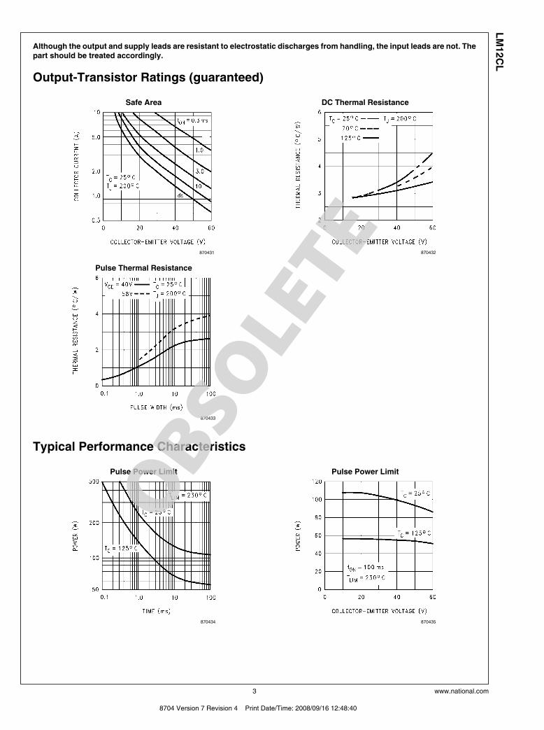
Although the output and supply leads are resistant to electrostatic discharges from handling, the input leads are not. Thepart should be treated accordingly.
Output-Transistor Ratings (guaranteed)
Safe Area
870431
DC Thermal Resistance
870432
Pulse Thermal Resistance
870433
Typical Performance Characteristics
Pulse Power Limit
870434
Pulse Power Limit
870435
3 www.national.com
8704 Version 7 Revision 4 Print Date/Time: 2008/09/16 12:48:40
LM
12C
L
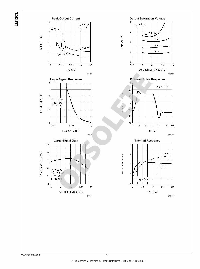
Peak Output Current
870436
Output Saturation Voltage
870437
Large Signal Response
870438
Follower Pulse Response
870439
Large Signal Gain
870440
Thermal Response
870441
www.national.com 4
8704 Version 7 Revision 4 Print Date/Time: 2008/09/16 12:48:40
LM
12C
L
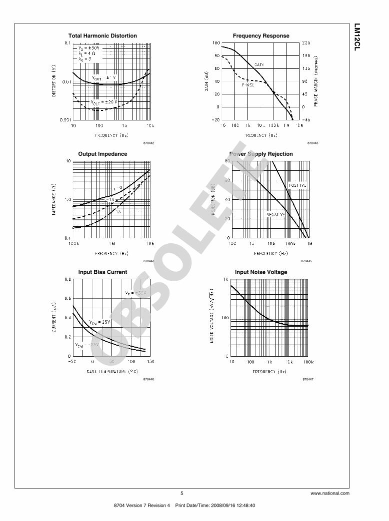
Total Harmonic Distortion
870442
Frequency Response
870443
Output Impedance
870444
Power Supply Rejection
870445
Input Bias Current
870446
Input Noise Voltage
870447
5 www.national.com
8704 Version 7 Revision 4 Print Date/Time: 2008/09/16 12:48:40
LM
12C
L
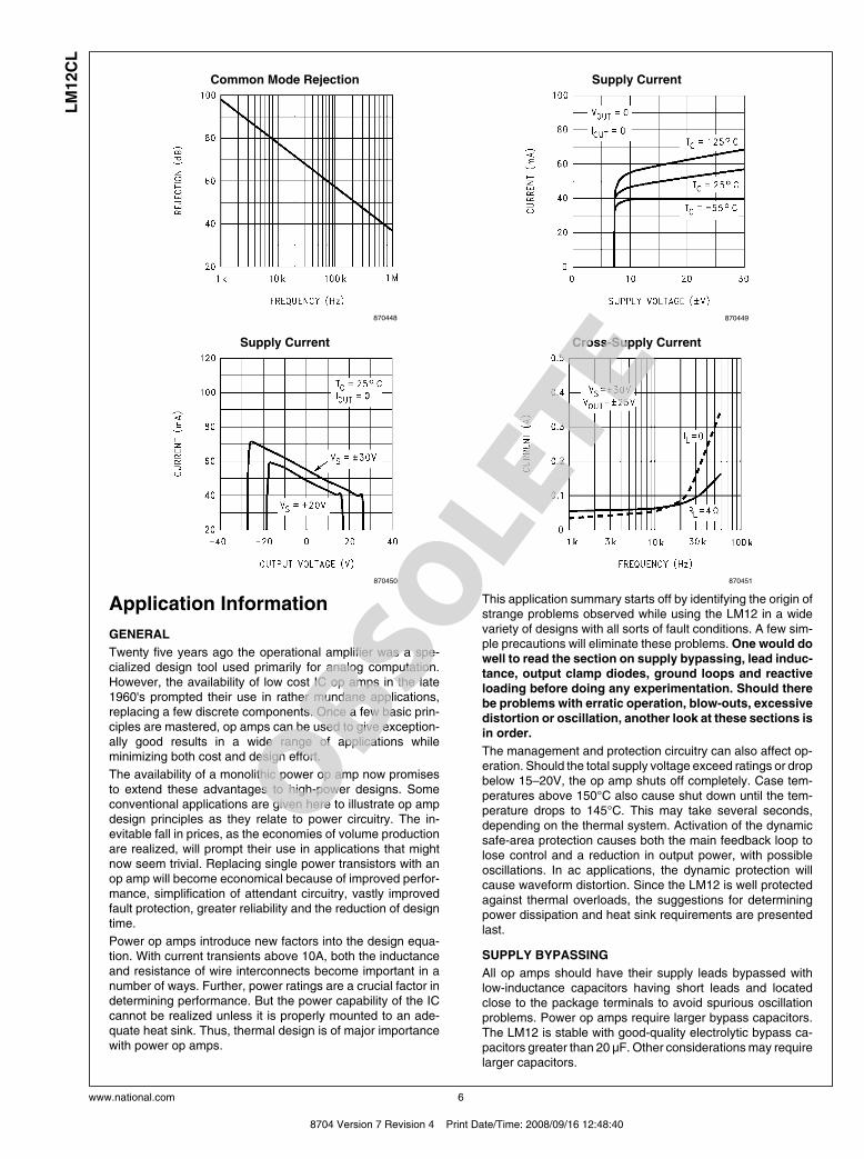
Common Mode Rejection
870448
Supply Current
870449
Supply Current
870450
Cross-Supply Current
870451
Application Information
GENERAL
Twenty five years ago the operational amplifier was a spe-cialized design tool used primarily for analog computation.However, the availability of low cost IC op amps in the late1960's prompted their use in rather mundane applications,replacing a few discrete components. Once a few basic prin-ciples are mastered, op amps can be used to give exception-ally good results in a wide range of applications whileminimizing both cost and design effort.
The availability of a monolithic power op amp now promisesto extend these advantages to high-power designs. Someconventional applications are given here to illustrate op ampdesign principles as they relate to power circuitry. The in-evitable fall in prices, as the economies of volume productionare realized, will prompt their use in applications that mightnow seem trivial. Replacing single power transistors with anop amp will become economical because of improved perfor-mance, simplification of attendant circuitry, vastly improvedfault protection, greater reliability and the reduction of designtime.
Power op amps introduce new factors into the design equa-tion. With current transients above 10A, both the inductanceand resistance of wire interconnects become important in anumber of ways. Further, power ratings are a crucial factor indetermining performance. But the power capability of the ICcannot be realized unless it is properly mounted to an ade-quate heat sink. Thus, thermal design is of major importancewith power op amps.
This application summary starts off by identifying the origin ofstrange problems observed while using the LM12 in a widevariety of designs with all sorts of fault conditions. A few sim-ple precautions will eliminate these problems. One would dowell to read the section on supply bypassing, lead induc-tance, output clamp diodes, ground loops and reactiveloading before doing any experimentation. Should therebe problems with erratic operation, blow-outs, excessivedistortion or oscillation, another look at these sections isin order.
The management and protection circuitry can also affect op-eration. Should the total supply voltage exceed ratings or dropbelow 15–20V, the op amp shuts off completely. Case tem-peratures above 150°C also cause shut down until the tem-perature drops to 145°C. This may take several seconds,depending on the thermal system. Activation of the dynamicsafe-area protection causes both the main feedback loop tolose control and a reduction in output power, with possibleoscillations. In ac applications, the dynamic protection willcause waveform distortion. Since the LM12 is well protectedagainst thermal overloads, the suggestions for determiningpower dissipation and heat sink requirements are presentedlast.
SUPPLY BYPASSING
All op amps should have their supply leads bypassed withlow-inductance capacitors having short leads and locatedclose to the package terminals to avoid spurious oscillationproblems. Power op amps require larger bypass capacitors.The LM12 is stable with good-quality electrolytic bypass ca-pacitors greater than 20 μF. Other considerations may requirelarger capacitors.
www.national.com 6
8704 Version 7 Revision 4 Print Date/Time: 2008/09/16 12:48:40
LM
12C
L
The current in the supply leads is a rectified component of theload current. If adequate bypassing is not provided, this dis-torted signal can be fed back into internal circuitry. Low dis-tortion at high frequencies requires that the supplies bebypassed with 470 μF or more, at the package terminals.
LEAD INDUCTANCE
With ordinary op amps, lead-inductance problems are usuallyrestricted to supply bypassing. Power op amps are also sen-sitive to inductance in the output lead, particularly with heavycapacitive loading. Feedback to the input should be taken di-rectly from the output terminal, minimizing common induc-tance with the load. Sensing to a remote load must beaccompanied by a high-frequency feedback path directly fromthe output terminal. Lead inductance can also cause voltagesurges on the supplies. With long leads to the power source,energy stored in the lead inductance when the output is short-ed can be dumped back into the supply bypass capacitorswhen the short is removed. The magnitude of this transient isreduced by increasing the size of the bypass capacitor nearthe IC. With 20 μF local bypass, these voltage surges are im-portant only if the lead length exceeds a couple feet (> 1 μHlead inductance). Twisting together the supply and groundleads minimizes the effect.
GROUND LOOPS
With fast, high-current circuitry, all sorts of problems can arisefrom improper grounding. In general, difficulties can be avoid-ed by returning all grounds separately to a common point.Sometimes this is impractical. When compromising, specialattention should be paid to the ground returns for the supplybypasses, load and input signal. Ground planes also help toprovide proper grounding.
Many problems unrelated to system performance can betraced to the grounding of line-operated test equipment usedfor system checkout. Hidden paths are particularly difficult tosort out when several pieces of test equipment are used butcan be minimized by using current probes or the new isolatedoscilloscope pre-amplifiers. Eliminating any direct groundconnection between the signal generator and the oscillo-scope synchronization input solves one common problem.
OUTPUT CLAMP DIODES
When a push-pull amplifier goes into power limit while drivingan inductive load, the stored energy in the load inductancecan drive the output outside the supplies. Although the LM12has internal clamp diodes that can handle several amperesfor a few milliseconds, extreme conditions can cause destruc-tion of the IC. The internal clamp diodes are imperfect in thatabout half the clamp current flows into the supply to which theoutput is clamped while the other half flows across the sup-plies. Therefore, the use of external diodes to clamp theoutput to the power supplies is strongly recommended. Thisis particularly important with higher supply voltages.
Experience has demonstrated that hard-wire shorting the out-put to the supplies can induce random failures if these exter-nal clamp diodes are not used and the supply voltages areabove ±20V. Therefore it is prudent to use outputclampdiodes even when the load is not particularly inductive. Thisalso applies to experimental setups in that blowouts havebeen observed when diodes were not used. In packagedequipment, it may be possible to eliminate these diodes, pro-viding that fault conditions can be controlled.
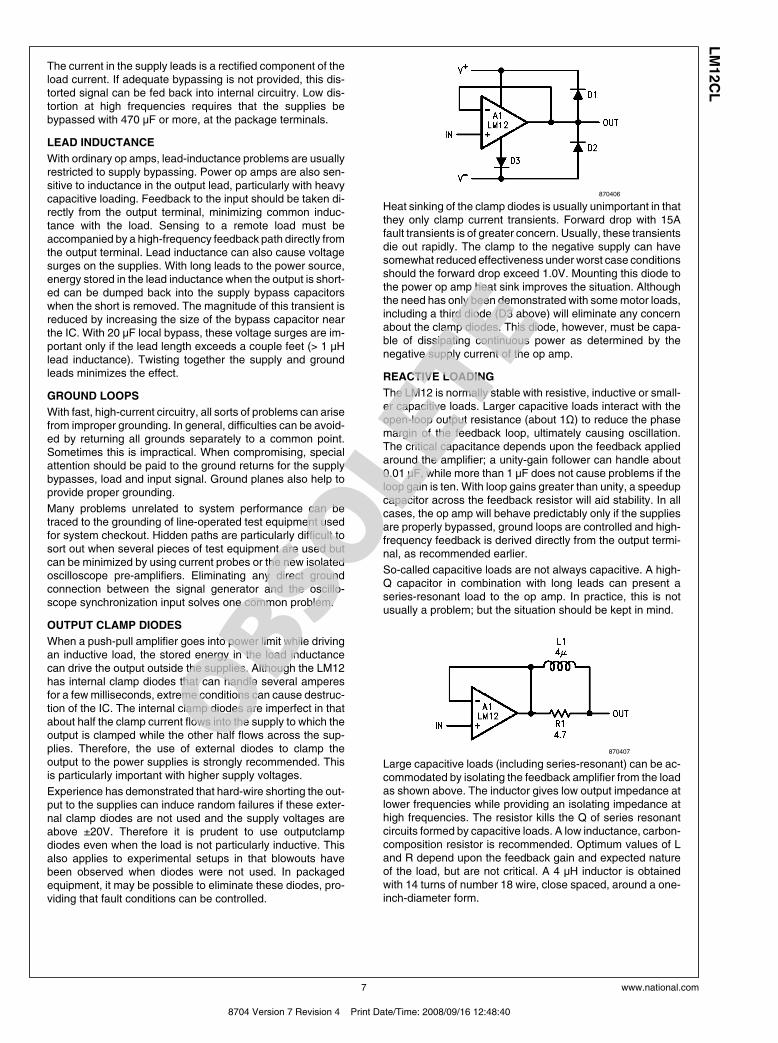
870406
Heat sinking of the clamp diodes is usually unimportant in thatthey only clamp current transients. Forward drop with 15Afault transients is of greater concern. Usually, these transientsdie out rapidly. The clamp to the negative supply can havesomewhat reduced effectiveness under worst case conditionsshould the forward drop exceed 1.0V. Mounting this diode tothe power op amp heat sink improves the situation. Althoughthe need has only been demonstrated with some motor loads,including a third diode (D3 above) will eliminate any concernabout the clamp diodes. This diode, however, must be capa-ble of dissipating continuous power as determined by thenegative supply current of the op amp.
REACTIVE LOADING
The LM12 is normally stable with resistive, inductive or small-er capacitive loads. Larger capacitive loads interact with theopen-loop output resistance (about 1Ω) to reduce the phasemargin of the feedback loop, ultimately causing oscillation.The critical capacitance depends upon the feedback appliedaround the amplifier; a unity-gain follower can handle about0.01 μF, while more than 1 μF does not cause problems if theloop gain is ten. With loop gains greater than unity, a speedupcapacitor across the feedback resistor will aid stability. In allcases, the op amp will behave predictably only if the suppliesare properly bypassed, ground loops are controlled and high-frequency feedback is derived directly from the output termi-nal, as recommended earlier.
So-called capacitive loads are not always capacitive. A high-Q capacitor in combination with long leads can present aseries-resonant load to the op amp. In practice, this is notusually a problem; but the situation should be kept in mind.
870407
Large capacitive loads (including series-resonant) can be ac-commodated by isolating the feedback amplifier from the loadas shown above. The inductor gives low output impedance atlower frequencies while providing an isolating impedance athigh frequencies. The resistor kills the Q of series resonantcircuits formed by capacitive loads. A low inductance, carbon-composition resistor is recommended. Optimum values of Land R depend upon the feedback gain and expected natureof the load, but are not critical. A 4 μH inductor is obtainedwith 14 turns of number 18 wire, close spaced, around a one-inch-diameter form.
7 www.national.com
8704 Version 7 Revision 4 Print Date/Time: 2008/09/16 12:48:40
LM
12C
L
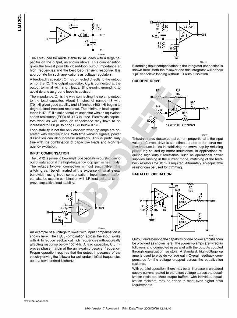
870408
The LM12 can be made stable for all loads with a large ca-pacitor on the output, as shown above. This compensationgives the lowest possible closed-loop output impedance athigh frequencies and the best load-transient response. It isappropriate for such applications as voltage regulators.
A feedback capacitor, C1, is connected directly to the outputpin of the IC. The output capacitor, C2, is connected at theoutput terminal with short leads. Single-point grounding toavoid dc and ac ground loops is advised.
The impedance, Z1, is the wire connecting the op amp outputto the load capacitor. About 3-inches of number-18 wire(70 nH) gives good stability and 18-inches (400 nH) begins todegrade load-transient response. The minimum load capaci-tance is 47 μF, if a solid-tantalum capacitor with an equivalentseries resistance (ESR) of 0.1Ω is used. Electrolytic capaci-tors work as well, although capacitance may have to beincreased to 200 μF to bring ESR below 0.1Ω.Loop stability is not the only concern when op amps are op-erated with reactive loads. With time-varying signals, powerdissipation can also increase markedly. This is particularlytrue with the combination of capacitive loads and high-fre-quency excitation.
INPUT COMPENSATION
The LM12 is prone to low-amplitude oscillation bursts comingout of saturation if the high-frequency loop gain is near unity.The voltage follower connection is most susceptible. Thisglitching can be eliminated at the expense of small-signalbandwidth using input compensation. Input compensationcan also be used in combination with LR load isolation to im-prove capacitive load stability.
870409
An example of a voltage follower with input compensation isshown here. The R2C2 combination across the input workswith R1 to reduce feedback at high frequencies without greatlyaffecting response below 100 kHz. A lead capacitor, C1, im-proves phase margin at the unity-gain crossover frequency.Proper operation requires that the output impedance of thecircuitry driving the follower be well under 1 kΩ at frequenciesup to a few hundred kilohertz.
870410
Extending input compensation to the integrator connection isshown here. Both the follower and this integrator will handle1 μF capacitive loading without LR output isolation.
CURRENT DRIVE
870411
This circuit provides an output current proportional to the inputvoltage. Current drive is sometimes preferred for servo mo-tors because it aids in stabilizing the servo loop by reducingphase lag caused by motor inductance. In applications re-quiring high output resistance, such as operational powersupplies running in the current mode, matching of the feed-back resistors to 0.01% is required. Alternately, an adjustableresistor can be used for trimming.
PARALLEL OPERATION
870412
Output drive beyond the capability of one power amplifier canbe provided as shown here. The power op amps are wired asfollowers and connected in parallel with the outputs coupledthrough equalization resistors. A standard, high-voltage opamp is used to provide voltage gain. Overall feedback com-pensates for the voltage dropped across the equalizationresistors.
With parallel operation, there may be an increase in unloadedsupply current related to the offset voltage across the equal-ization resistors. More output buffers, with individual equal-ization resistors, may be added to meet even higher driverequirements.
www.national.com 8
8704 Version 7 Revision 4 Print Date/Time: 2008/09/16 12:48:40
LM
12C
L
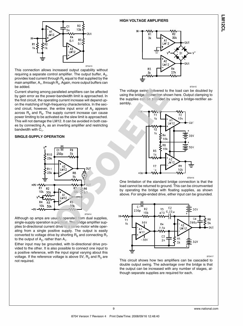
870413
This connection allows increased output capability withoutrequiring a separate control amplifier. The output buffer, A2,provides load current through R5 equal to that supplied by themain amplifier, A1, through R4. Again, more output buffers canbe added.
Current sharing among paralleled amplifiers can be affectedby gain error as the power-bandwidth limit is approached. Inthe first circuit, the operating current increase will depend up-on the matching of high-frequency characteristics. In the sec-ond circuit, however, the entire input error of A2 appearsacross R4 and R5. The supply current increase can causepower limiting to be activated as the slew limit is approached.This will not damage the LM12. It can be avoided in both cas-es by connecting A1 as an inverting amplifier and restrictingbandwidth with C1.
SINGLE-SUPPLY OPERATION
870414
Although op amps are usually operated from dual supplies,single-supply operation is practical. This bridge amplifier sup-plies bi-directional current drive to a servo motor while oper-ating from a single positive supply. The output is easilyconverted to voltage drive by shorting R6 and connecting R7to the output of A2, rather than A1.
Either input may be grounded, with bi-directional drive pro-vided to the other. It is also possible to connect one input toa positive reference, with the input signal varying about thisvoltage. If the reference voltage is above 5V, R2 and R3 arenot required.
HIGH VOLTAGE AMPLIFIERS
870415
The voltage swing delivered to the load can be doubled byusing the bridge connection shown here. Output clamping tothe supplies can be provided by using a bridge-rectifier as-sembly.
870416
One limitation of the standard bridge connection is that theload cannot be returned to ground. This can be circumventedby operating the bridge with floating supplies, as shownabove. For single-ended drive, either input can be grounded.
870417
This circuit shows how two amplifiers can be cascaded todouble output swing. The advantage over the bridge is thatthe output can be increased with any number of stages, al-though separate supplies are required for each.
9 www.national.com
8704 Version 7 Revision 4 Print Date/Time: 2008/09/16 12:48:40
LM
12C
L
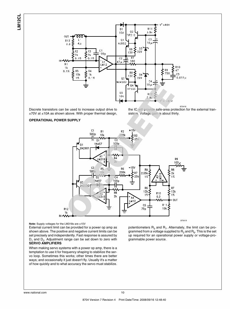
870418
Discrete transistors can be used to increase output drive to±70V at ±10A as shown above. With proper thermal design,
the IC will provide safe-area protection for the external tran-sistors. Voltage gain is about thirty.
OPERATIONAL POWER SUPPLY
870419
Note: Supply voltages for the LM318s are ±15V
External current limit can be provided for a power op amp asshown above. The positive and negative current limits can beset precisely and independently. Fast response is assured byD1 and D2. Adjustment range can be set down to zero with
potentiometers R3 and R7. Alternately, the limit can be pro-grammed from a voltage supplied to R2 and R6. This is the setup required for an operational power supply or voltage-pro-grammable power source.
SERVO AMPLIFIERS
When making servo systems with a power op amp, there is atemptation to use it for frequency shaping to stabilize the ser-vo loop. Sometimes this works; other times there are betterways; and occasionally it just doesn't fly. Usually it's a matterof how quickly and to what accuracy the servo must stabilize.
www.national.com 10
8704 Version 7 Revision 4 Print Date/Time: 2008/09/16 12:48:40
LM
12C
L
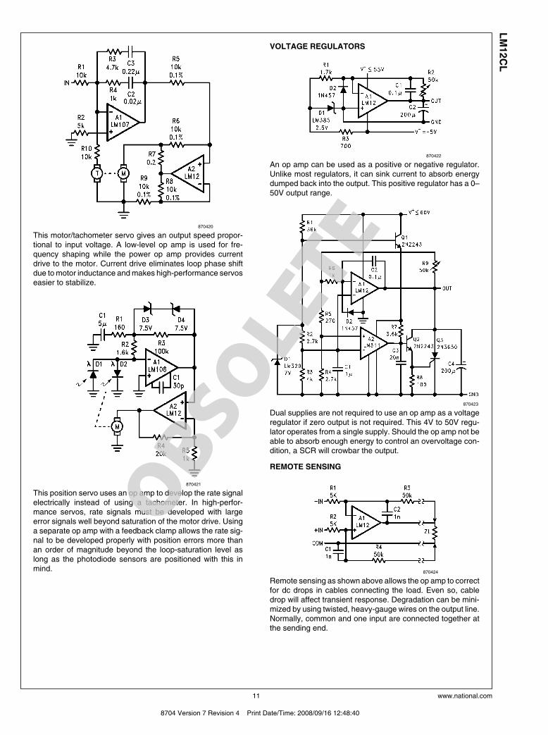
870420
This motor/tachometer servo gives an output speed propor-tional to input voltage. A low-level op amp is used for fre-quency shaping while the power op amp provides currentdrive to the motor. Current drive eliminates loop phase shiftdue to motor inductance and makes high-performance servoseasier to stabilize.
870421
This position servo uses an op amp to develop the rate signalelectrically instead of using a tachometer. In high-perfor-mance servos, rate signals must be developed with largeerror signals well beyond saturation of the motor drive. Usinga separate op amp with a feedback clamp allows the rate sig-nal to be developed properly with position errors more thanan order of magnitude beyond the loop-saturation level aslong as the photodiode sensors are positioned with this inmind.
VOLTAGE REGULATORS
870422
An op amp can be used as a positive or negative regulator.Unlike most regulators, it can sink current to absorb energydumped back into the output. This positive regulator has a 0–50V output range.
870423
Dual supplies are not required to use an op amp as a voltageregulator if zero output is not required. This 4V to 50V regu-lator operates from a single supply. Should the op amp not beable to absorb enough energy to control an overvoltage con-dition, a SCR will crowbar the output.
REMOTE SENSING
870424
Remote sensing as shown above allows the op amp to correctfor dc drops in cables connecting the load. Even so, cabledrop will affect transient response. Degradation can be mini-mized by using twisted, heavy-gauge wires on the output line.Normally, common and one input are connected together atthe sending end.
11 www.national.com
8704 Version 7 Revision 4 Print Date/Time: 2008/09/16 12:48:40
LM
12C
L
AUDIO AMPLIFIERS
870425
A power amplifier suitable for use in high-quality audio equip-ment is shown above. Harmonic distortion is about 0.01-percent. Intermodulation distortion (60 Hz/7 kHz, 4:1) mea-sured 0.015-percent. Transient response and saturationrecovery are clean, and the 9 V/μs slew rate of the LM12 vir-tually eliminates transient intermodulation distortion. Usingseparate amplifiers to drive low- and high-frequency speakersgets rid of high-level crossover networks and attenuators.Further, it prevents clipping on the low-frequency channelfrom distorting the high frequencies.
DETERMINING MAXIMUM DISSIPATION
It is a simple matter to establish power requirements for anop amp driving a resistive load at frequencies well below10 Hz. Maximum dissipation occurs when the output is at one-half the supply voltage with high-line conditions. The individ-ual output transistors must be rated to handle this powercontinuously at the maximum expected case temperature.The power rating is limited by the maximum junction temper-ature as determined by
TJ = TC + PDISS θJC,
where TC is the case temperature as measured at the centerof the package bottom, PDISS is the maximum power dissipa-tion and θJC is the thermal resistance at the operating voltageof the output transistor. Recommended maximum junctiontemperatures are 200°C within the power transistor and 150°C for the control circuitry.
If there is ripple on the supply bus, it is valid to use the averagevalue in worst-case calculations as long as the peak rating ofthe power transistor is not exceeded at the ripple peak. With120 Hz ripple, this is 1.5 times the continuous power rating.
Dissipation requirements are not so easily established withtime varying output signals, especially with reactive loads.Both peak and continuous dissipation ratings must be takeninto account, and these depend on the signal waveform aswell as load characteristics.
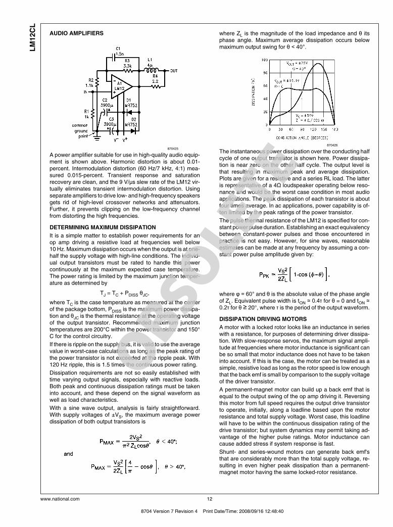
With a sine wave output, analysis is fairly straightforward.With supply voltages of ±VS, the maximum average powerdissipation of both output transistors is
where ZL is the magnitude of the load impedance and θ itsphase angle. Maximum average dissipation occurs belowmaximum output swing for θ < 40°.
870426
The instantaneous power dissipation over the conducting halfcycle of one output transistor is shown here. Power dissipa-tion is near zero on the other half cycle. The output level isthat resulting in maximum peak and average dissipation.Plots are given for a resistive and a series RL load. The latteris representative of a 4Ω loudspeaker operating below reso-nance and would be the worst case condition in most audioapplications. The peak dissipation of each transistor is aboutfour times average. In ac applications, power capability is of-ten limited by the peak ratings of the power transistor.
The pulse thermal resistance of the LM12 is specified for con-stant power pulse duration. Establishing an exact equivalencybetween constant-power pulses and those encountered inpractice is not easy. However, for sine waves, reasonableestimates can be made at any frequency by assuming a con-stant power pulse amplitude given by:
where φ = 60° and θ is the absolute value of the phase angleof ZL. Equivalent pulse width is tON ≃ 0.4τ for θ = 0 and tON ≃0.2τ for θ ≥ 20°, where τ is the period of the output waveform.
DISSIPATION DRIVING MOTORS
A motor with a locked rotor looks like an inductance in serieswith a resistance, for purposes of determining driver dissipa-tion. With slow-response servos, the maximum signal ampli-tude at frequencies where motor inductance is significant canbe so small that motor inductance does not have to be takeninto account. If this is the case, the motor can be treated as asimple, resistive load as long as the rotor speed is low enoughthat the back emf is small by comparison to the supply voltageof the driver transistor.
A permanent-magnet motor can build up a back emf that isequal to the output swing of the op amp driving it. Reversingthis motor from full speed requires the output drive transistorto operate, initially, along a loadline based upon the motorresistance and total supply voltage. Worst case, this loadlinewill have to be within the continuous dissipation rating of thedrive transistor; but system dynamics may permit taking ad-vantage of the higher pulse ratings. Motor inductance cancause added stress if system response is fast.
Shunt- and series-wound motors can generate back emf'sthat are considerably more than the total supply voltage, re-sulting in even higher peak dissipation than a permanent-magnet motor having the same locked-rotor resistance.
www.national.com 12
8704 Version 7 Revision 4 Print Date/Time: 2008/09/16 12:48:40
LM
12C
L
VOLTAGE REGULATOR DISSIPATION
The pass transistor dissipation of a voltage regulator is easilydetermined in the operating mode. Maximum continuous dis-sipation occurs with high line voltage and maximum loadcurrent. As discussed earlier, ripple voltage can be averagedif peak ratings are not exceeded; however, a higher averagevoltage will be required to insure that the pass transistor doesnot saturate at the ripple minimum.
Conditions during start-up can be more complex. If the inputvoltage increases slowly such that the regulator does not gointo current limit charging output capacitance, there are noproblems. If not, load capacitance and load characteristicsmust be taken into account. This is also the case if automaticrestart is required in recovering from overloads.
Automatic restart or start-up with fast-rising input voltagescannot be guaranteed unless the continuous dissipation rat-ing of the pass transistor is adequate to supply the loadcurrent continuously at all voltages below the regulated outputvoltage. In this regard, the LM12 performs much better thanIC regulators using foldback current limit, especially with high-line input voltage above 20V.
POWER LIMITING
870427
Should the power ratings of the LM12 be exceeded, dynamicsafe-area protection is activated. Waveforms with this powerlimiting are shown for the LM12 driving ±26V at 30 Hz into3Ω in series with 24 mH (θ = 45°). With an inductive load, theoutput clamps to the supplies in power limit, as above. Withresistive loads, the output voltage drops in limit. Behavior withmore complex RCL loads is between these extremes.
Secondary thermal limit is activated should the case temper-ature exceed 150°C. This thermal limit shuts down the ICcompletely (open output) until the case temperature drops toabout 145°C. Recovery may take several seconds.
POWER SUPPLIES
Power op amps do not require regulated supplies. However,the worst-case output power is determined by the low-linesupply voltage in the ripple trough. The worst-case powerdissipation is established by the average supply voltage withhigh-line conditions. The loss in power output that can beguaranteed is the square of the ratio of these two voltages.
Relatively simple off-line switching power supplies can pro-vide voltage conversion, line isolation and 5-percent regula-tion while reducing size and weight.
The regulation against ripple and line variations can providea substantial increase in the power output that can be guar-anteed under worst-case conditions. In addition, switchingpower supplies can convert low-voltage power sources suchas automotive batteries up to regulated, dual, high-voltagesupplies optimized for powering power op amps.
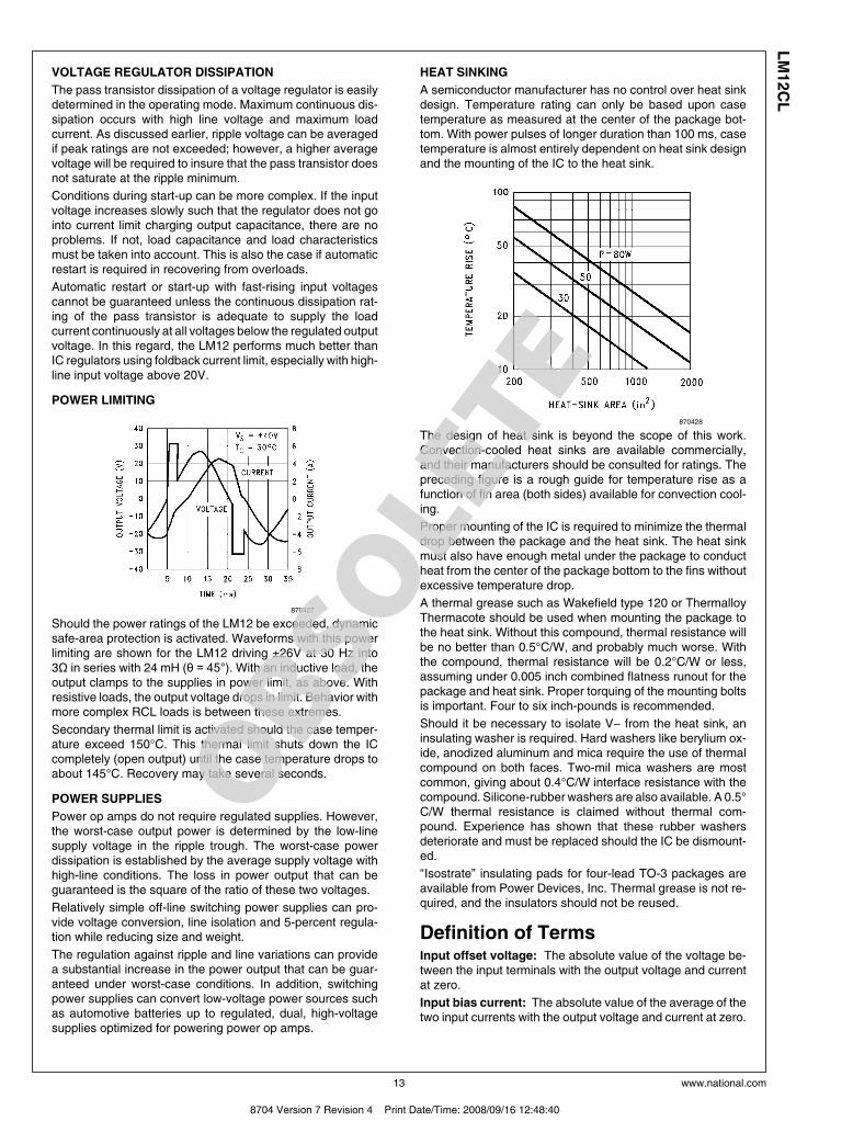
HEAT SINKING
A semiconductor manufacturer has no control over heat sinkdesign. Temperature rating can only be based upon casetemperature as measured at the center of the package bot-tom. With power pulses of longer duration than 100 ms, casetemperature is almost entirely dependent on heat sink designand the mounting of the IC to the heat sink.
870428
The design of heat sink is beyond the scope of this work.Convection-cooled heat sinks are available commercially,and their manufacturers should be consulted for ratings. Thepreceding figure is a rough guide for temperature rise as afunction of fin area (both sides) available for convection cool-ing.
Proper mounting of the IC is required to minimize the thermaldrop between the package and the heat sink. The heat sinkmust also have enough metal under the package to conductheat from the center of the package bottom to the fins withoutexcessive temperature drop.
A thermal grease such as Wakefield type 120 or ThermalloyThermacote should be used when mounting the package tothe heat sink. Without this compound, thermal resistance willbe no better than 0.5°C/W, and probably much worse. Withthe compound, thermal resistance will be 0.2°C/W or less,assuming under 0.005 inch combined flatness runout for thepackage and heat sink. Proper torquing of the mounting boltsis important. Four to six inch-pounds is recommended.
Should it be necessary to isolate V− from the heat sink, aninsulating washer is required. Hard washers like berylium ox-ide, anodized aluminum and mica require the use of thermalcompound on both faces. Two-mil mica washers are mostcommon, giving about 0.4°C/W interface resistance with thecompound. Silicone-rubber washers are also available. A 0.5°C/W thermal resistance is claimed without thermal com-pound. Experience has shown that these rubber washersdeteriorate and must be replaced should the IC be dismount-ed.
“Isostrate” insulating pads for four-lead TO-3 packages areavailable from Power Devices, Inc. Thermal grease is not re-quired, and the insulators should not be reused.
Definition of TermsInput offset voltage: The absolute value of the voltage be-tween the input terminals with the output voltage and currentat zero.
Input bias current: The absolute value of the average of thetwo input currents with the output voltage and current at zero.
13 www.national.com
8704 Version 7 Revision 4 Print Date/Time: 2008/09/16 12:48:40
LM
12C
L
Input offset current: The absolute value of the difference inthe two input currents with the output voltage and current atzero.
Common-mode rejection: The ratio of the input voltagerange to the change in offset voltage between the extremes.
Supply-voltage rejection: The ratio of the specified supply-voltage change to the change in offset voltage between theextremes.
Output saturation threshold: The output swing limit for aspecified input drive beyond that required for zero output. It ismeasured with respect to the supply to which the output isswinging.
Large signal voltage gain: The ratio of the output voltageswing to the differential input voltage required to drive theoutput from zero to either swing limit. The output swing limitis the supply voltage less a specified quasi-saturation voltage.A pulse of short enough duration to minimize thermal effectsis used as a measurement signal.
Thermal gradient feedback: The input offset voltagechange caused by thermal gradients generated by heating ofthe output transistors, but not the package. This effect is de-
layed by several milliseconds and results in increased gainerror below 100 Hz.
Output-current limit: The output current with a fixed outputvoltage and a large input overdrive. The limiting current dropswith time once the protection circuitry is activated.
Power dissipation rating: The power that can be dissipatedfor a specified time interval without activating the protectioncircuitry. For time intervals in excess of 100 ms, dissipationcapability is determined by heat sinking of the IC packagerather than by the IC itself.
Thermal resistance: The peak, junction-temperature rise,per unit of internal power dissipation, above the case tem-perature as measured at the center of the package bottom.The dc thermal resistance applies when one output transistoris operating continuously. The ac thermal resistance applieswith the output transistors conducting alternately at a highenough frequency that the peak capability of neither transistoris exceeded.
Supply current: The current required from the power sourceto operate the amplifier with the output voltage and current atzero.
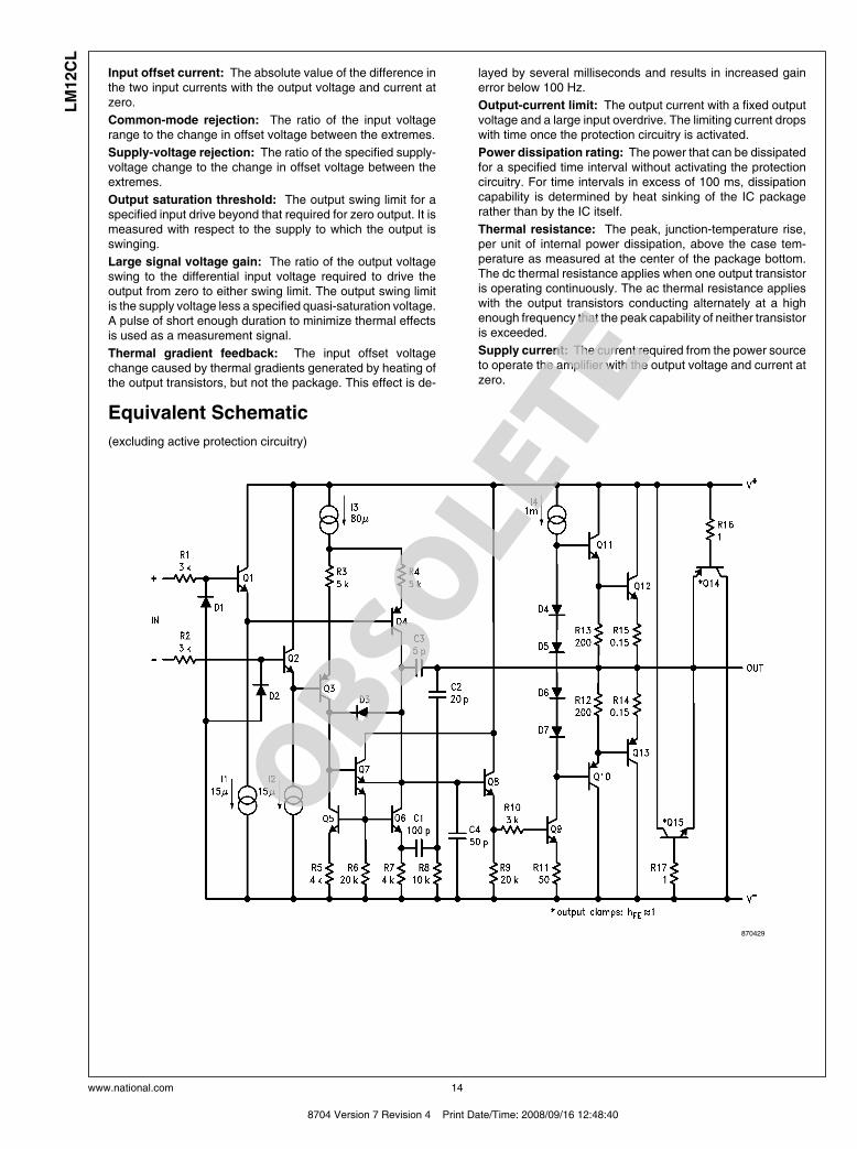
Equivalent Schematic
(excluding active protection circuitry)
870429
www.national.com 14
8704 Version 7 Revision 4 Print Date/Time: 2008/09/16 12:48:40
LM
12C
L
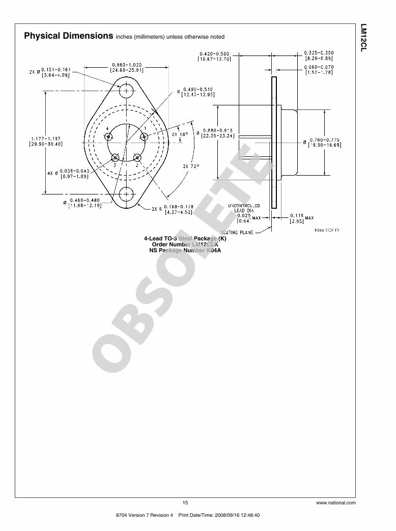
Physical Dimensions inches (millimeters) unless otherwise noted
4-Lead TO-3 Steel Package (K)Order Number LM12CLK
NS Package Number K04A
15 www.national.com
8704 Version 7 Revision 4 Print Date/Time: 2008/09/16 12:48:40
LM
12C
L
NotesL
M12C
L 8
0W
Op
era
tio
nal A
mp
lifi
er
For more National Semiconductor product information and proven design tools, visit the following Web sites at:
Products Design Support
Amplifiers www.national.com/amplifiers WEBENCH www.national.com/webench
Audio www.national.com/audio Analog University www.national.com/AU
Clock Conditioners www.national.com/timing App Notes www.national.com/appnotes
Data Converters www.national.com/adc Distributors www.national.com/contacts
Displays www.national.com/displays Green Compliance www.national.com/quality/green
Ethernet www.national.com/ethernet Packaging www.national.com/packaging
Interface www.national.com/interface Quality and Reliability www.national.com/quality
LVDS www.national.com/lvds Reference Designs www.national.com/refdesigns
Power Management www.national.com/power Feedback www.national.com/feedback
Switching Regulators www.national.com/switchers
LDOs www.national.com/ldo
LED Lighting www.national.com/led
PowerWise www.national.com/powerwise
Serial Digital Interface (SDI) www.national.com/sdi
Temperature Sensors www.national.com/tempsensors
Wireless (PLL/VCO) www.national.com/wireless
THE CONTENTS OF THIS DOCUMENT ARE PROVIDED IN CONNECTION WITH NATIONAL SEMICONDUCTOR CORPORATION(“NATIONAL”) PRODUCTS. NATIONAL MAKES NO REPRESENTATIONS OR WARRANTIES WITH RESPECT TO THE ACCURACYOR COMPLETENESS OF THE CONTENTS OF THIS PUBLICATION AND RESERVES THE RIGHT TO MAKE CHANGES TOSPECIFICATIONS AND PRODUCT DESCRIPTIONS AT ANY TIME WITHOUT NOTICE. NO LICENSE, WHETHER EXPRESS,IMPLIED, ARISING BY ESTOPPEL OR OTHERWISE, TO ANY INTELLECTUAL PROPERTY RIGHTS IS GRANTED BY THISDOCUMENT.
TESTING AND OTHER QUALITY CONTROLS ARE USED TO THE EXTENT NATIONAL DEEMS NECESSARY TO SUPPORTNATIONAL’S PRODUCT WARRANTY. EXCEPT WHERE MANDATED BY GOVERNMENT REQUIREMENTS, TESTING OF ALLPARAMETERS OF EACH PRODUCT IS NOT NECESSARILY PERFORMED. NATIONAL ASSUMES NO LIABILITY FORAPPLICATIONS ASSISTANCE OR BUYER PRODUCT DESIGN. BUYERS ARE RESPONSIBLE FOR THEIR PRODUCTS ANDAPPLICATIONS USING NATIONAL COMPONENTS. PRIOR TO USING OR DISTRIBUTING ANY PRODUCTS THAT INCLUDENATIONAL COMPONENTS, BUYERS SHOULD PROVIDE ADEQUATE DESIGN, TESTING AND OPERATING SAFEGUARDS.
EXCEPT AS PROVIDED IN NATIONAL’S TERMS AND CONDITIONS OF SALE FOR SUCH PRODUCTS, NATIONAL ASSUMES NOLIABILITY WHATSOEVER, AND NATIONAL DISCLAIMS ANY EXPRESS OR IMPLIED WARRANTY RELATING TO THE SALEAND/OR USE OF NATIONAL PRODUCTS INCLUDING LIABILITY OR WARRANTIES RELATING TO FITNESS FOR A PARTICULARPURPOSE, MERCHANTABILITY, OR INFRINGEMENT OF ANY PATENT, COPYRIGHT OR OTHER INTELLECTUAL PROPERTYRIGHT.
LIFE SUPPORT POLICY
NATIONAL’S PRODUCTS ARE NOT AUTHORIZED FOR USE AS CRITICAL COMPONENTS IN LIFE SUPPORT DEVICES ORSYSTEMS WITHOUT THE EXPRESS PRIOR WRITTEN APPROVAL OF THE CHIEF EXECUTIVE OFFICER AND GENERALCOUNSEL OF NATIONAL SEMICONDUCTOR CORPORATION. As used herein:
Life support devices or systems are devices which (a) are intended for surgical implant into the body, or (b) support or sustain life andwhose failure to perform when properly used in accordance with instructions for use provided in the labeling can be reasonably expectedto result in a significant injury to the user. A critical component is any component in a life support device or system whose failure to performcan be reasonably expected to cause the failure of the life support device or system or to affect its safety or effectiveness.
National Semiconductor and the National Semiconductor logo are registered trademarks of National Semiconductor Corporation. All otherbrand or product names may be trademarks or registered trademarks of their respective holders.
Copyright© 2008 National Semiconductor Corporation
For the most current product information visit us at www.national.com
National SemiconductorAmericas TechnicalSupport CenterEmail: [email protected]: 1-800-272-9959
National Semiconductor EuropeTechnical Support CenterEmail: [email protected] Tel: +49 (0) 180 5010 771English Tel: +44 (0) 870 850 4288
National Semiconductor AsiaPacific Technical Support CenterEmail: [email protected]
National Semiconductor JapanTechnical Support CenterEmail: [email protected]
www.national.com
8704 Version 7 Revision 4 Print Date/Time: 2008/09/16 12:48:40

IMPORTANT NOTICE
Texas Instruments Incorporated and its subsidiaries (TI) reserve the right to make corrections, modifications, enhancements, improvements,and other changes to its products and services at any time and to discontinue any product or service without notice. Customers shouldobtain the latest relevant information before placing orders and should verify that such information is current and complete. All products aresold subject to TI’s terms and conditions of sale supplied at the time of order acknowledgment.
TI warrants performance of its hardware products to the specifications applicable at the time of sale in accordance with TI’s standardwarranty. Testing and other quality control techniques are used to the extent TI deems necessary to support this warranty. Except wheremandated by government requirements, testing of all parameters of each product is not necessarily performed.
TI assumes no liability for applications assistance or customer product design. Customers are responsible for their products andapplications using TI components. To minimize the risks associated with customer products and applications, customers should provideadequate design and operating safeguards.
TI does not warrant or represent that any license, either express or implied, is granted under any TI patent right, copyright, mask work right,or other TI intellectual property right relating to any combination, machine, or process in which TI products or services are used. Informationpublished by TI regarding third-party products or services does not constitute a license from TI to use such products or services or awarranty or endorsement thereof. Use of such information may require a license from a third party under the patents or other intellectualproperty of the third party, or a license from TI under the patents or other intellectual property of TI.
Reproduction of TI information in TI data books or data sheets is permissible only if reproduction is without alteration and is accompaniedby all associated warranties, conditions, limitations, and notices. Reproduction of this information with alteration is an unfair and deceptivebusiness practice. TI is not responsible or liable for such altered documentation. Information of third parties may be subject to additionalrestrictions.
Resale of TI products or services with statements different from or beyond the parameters stated by TI for that product or service voids allexpress and any implied warranties for the associated TI product or service and is an unfair and deceptive business practice. TI is notresponsible or liable for any such statements.
TI products are not authorized for use in safety-critical applications (such as life support) where a failure of the TI product would reasonablybe expected to cause severe personal injury or death, unless officers of the parties have executed an agreement specifically governingsuch use. Buyers represent that they have all necessary expertise in the safety and regulatory ramifications of their applications, andacknowledge and agree that they are solely responsible for all legal, regulatory and safety-related requirements concerning their productsand any use of TI products in such safety-critical applications, notwithstanding any applications-related information or support that may beprovided by TI. Further, Buyers must fully indemnify TI and its representatives against any damages arising out of the use of TI products insuch safety-critical applications.
TI products are neither designed nor intended for use in military/aerospace applications or environments unless the TI products arespecifically designated by TI as military-grade or "enhanced plastic." Only products designated by TI as military-grade meet militaryspecifications. Buyers acknowledge and agree that any such use of TI products which TI has not designated as military-grade is solely atthe Buyer's risk, and that they are solely responsible for compliance with all legal and regulatory requirements in connection with such use.
TI products are neither designed nor intended for use in automotive applications or environments unless the specific TI products aredesignated by TI as compliant with ISO/TS 16949 requirements. Buyers acknowledge and agree that, if they use any non-designatedproducts in automotive applications, TI will not be responsible for any failure to meet such requirements.
Following are URLs where you can obtain information on other Texas Instruments products and application solutions:
Products Applications
Audio www.ti.com/audio Communications and Telecom www.ti.com/communications
Amplifiers amplifier.ti.com Computers and Peripherals www.ti.com/computers
Data Converters dataconverter.ti.com Consumer Electronics www.ti.com/consumer-apps
DLP® Products www.dlp.com Energy and Lighting www.ti.com/energy
DSP dsp.ti.com Industrial www.ti.com/industrial
Clocks and Timers www.ti.com/clocks Medical www.ti.com/medical
Interface interface.ti.com Security www.ti.com/security
Logic logic.ti.com Space, Avionics and Defense www.ti.com/space-avionics-defense
Power Mgmt power.ti.com Transportation and Automotive www.ti.com/automotive
Microcontrollers microcontroller.ti.com Video and Imaging www.ti.com/video
RFID www.ti-rfid.com
OMAP Mobile Processors www.ti.com/omap
Wireless Connectivity www.ti.com/wirelessconnectivity
TI E2E Community Home Page e2e.ti.com
Mailing Address: Texas Instruments, Post Office Box 655303, Dallas, Texas 75265Copyright © 2011, Texas Instruments Incorporated


![SKC32.61 Datasheet en[1]](https://static.fdocument.org/doc/165x107/544dd02daf7959f3138b5162/skc3261-datasheet-en1.jpg)