Datasheet μPD44164184B
33
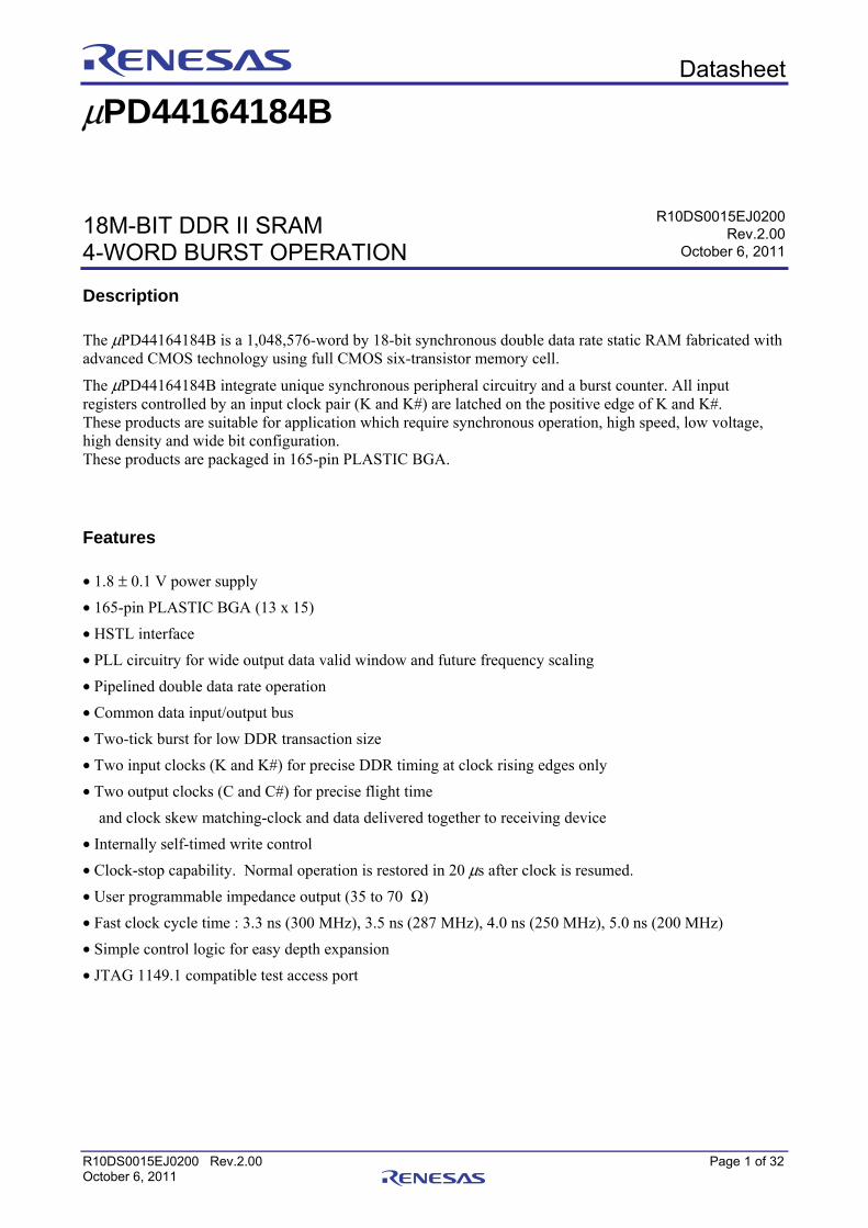
R10DS0015EJ0200 Rev.2.00 Page 1 of 32 October 6, 2011 Datasheet μPD44164184B 18M-BIT DDR II SRAM 4-WORD BURST OPERATION Description The μPD44164184B is a 1,048,576-word by 18-bit synchronous double data rate static RAM fabricated with advanced CMOS technology using full CMOS six-transistor memory cell. The μPD44164184B integrate unique synchronous peripheral circuitry and a burst counter. All input registers controlled by an input clock pair (K and K#) are latched on the positive edge of K and K#. These products are suitable for application which require synchronous operation, high speed, low voltage, high density and wide bit configuration. These products are packaged in 165-pin PLASTIC BGA. Features • 1.8 ± 0.1 V power supply • 165-pin PLASTIC BGA (13 x 15) • HSTL interface • PLL circuitry for wide output data valid window and future frequency scaling • Pipelined double data rate operation • Common data input/output bus • Two-tick burst for low DDR transaction size • Two input clocks (K and K#) for precise DDR timing at clock rising edges only • Two output clocks (C and C#) for precise flight time and clock skew matching-clock and data delivered together to receiving device • Internally self-timed write control • Clock-stop capability. Normal operation is restored in 20 μs after clock is resumed. • User programmable impedance output (35 to 70 Ω) • Fast clock cycle time : 3.3 ns (300 MHz), 3.5 ns (287 MHz), 4.0 ns (250 MHz), 5.0 ns (200 MHz) • Simple control logic for easy depth expansion • JTAG 1149.1 compatible test access port R10DS0015EJ0200 Rev.2.00 October 6, 2011
Transcript of Datasheet μPD44164184B
R10DS0015EJ0200 Rev.2.00 Page 1 of 32 October 6, 2011
Datasheet
μPD44164184B 18M-BIT DDR II SRAM 4-WORD BURST OPERATION Description
The μPD44164184B is a 1,048,576-word by 18-bit synchronous double data rate static RAM fabricated with advanced CMOS technology using full CMOS six-transistor memory cell.
The μPD44164184B integrate unique synchronous peripheral circuitry and a burst counter. All input registers controlled by an input clock pair (K and K#) are latched on the positive edge of K and K#. These products are suitable for application which require synchronous operation, high speed, low voltage, high density and wide bit configuration. These products are packaged in 165-pin PLASTIC BGA.
Features • 1.8 ± 0.1 V power supply • 165-pin PLASTIC BGA (13 x 15) • HSTL interface • PLL circuitry for wide output data valid window and future frequency scaling • Pipelined double data rate operation • Common data input/output bus • Two-tick burst for low DDR transaction size • Two input clocks (K and K#) for precise DDR timing at clock rising edges only • Two output clocks (C and C#) for precise flight time and clock skew matching-clock and data delivered together to receiving device • Internally self-timed write control • Clock-stop capability. Normal operation is restored in 20 μs after clock is resumed. • User programmable impedance output (35 to 70 Ω) • Fast clock cycle time : 3.3 ns (300 MHz), 3.5 ns (287 MHz), 4.0 ns (250 MHz), 5.0 ns (200 MHz) • Simple control logic for easy depth expansion • JTAG 1149.1 compatible test access port
R10DS0015EJ0200Rev.2.00
October 6, 2011
μPD44164184B
R10DS0015EJ0200 Rev.2.00 Page 2 of 32 October 6, 2011
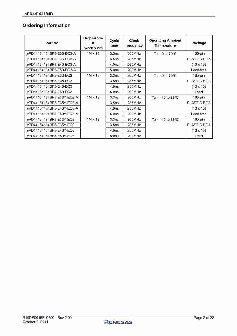
Ordering Information
Part No. Organizatio
n (word x bit)
Cycle time
Clock frequency
Operating Ambient Temperature
Package
μPD44164184BF5-E33-EQ3-A 1M x 18 3.3ns 300MHz Ta = 0 to 70°C 165-pin μPD44164184BF5-E35-EQ3-A 3.5ns 287MHz PLASTIC BGAμPD44164184BF5-E40-EQ3-A 4.0ns 250MHz (13 x 15) μPD44164184BF5-E50-EQ3-A 5.0ns 200MHz Lead-free μPD44164184BF5-E33-EQ3 1M x 18 3.3ns 300MHz Ta = 0 to 70°C 165-pin μPD44164184BF5-E35-EQ3 3.5ns 287MHz PLASTIC BGAμPD44164184BF5-E40-EQ3 4.0ns 250MHz (13 x 15) μPD44164184BF5-E50-EQ3 5.0ns 200MHz Lead μPD44164184BF5-E33Y-EQ3-A 1M x 18 3.3ns 300MHz Ta = −40 to 85°C 165-pin μPD44164184BF5-E35Y-EQ3-A 3.5ns 287MHz PLASTIC BGAμPD44164184BF5-E40Y-EQ3-A 4.0ns 250MHz (13 x 15) μPD44164184BF5-E50Y-EQ3-A 5.0ns 200MHz Lead-free μPD44164184BF5-E33Y-EQ3 1M x 18 3.3ns 300MHz Ta = −40 to 85°C 165-pin μPD44164184BF5-E35Y-EQ3 3.5ns 287MHz PLASTIC BGAμPD44164184BF5-E40Y-EQ3 4.0ns 250MHz (13 x 15) μPD44164184BF5-E50Y-EQ3 5.0ns 200MHz Lead
μPD44164184B
R10DS0015EJ0200 Rev.2.00 Page 3 of 32 October 6, 2011
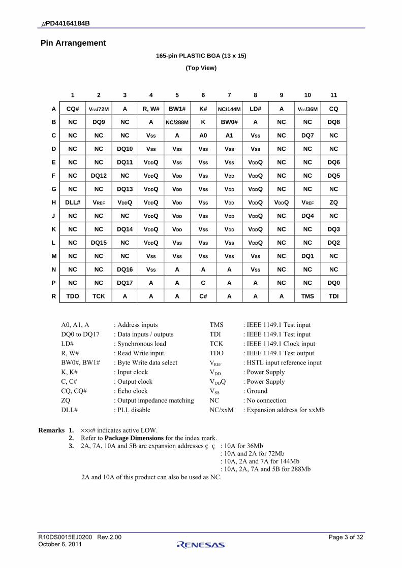
Pin Arrangement 165-pin PLASTIC BGA (13 x 15)
(Top View)
1 2 3 4 5 6 7 8 9 10 11
A CQ# VSS/72M A R, W# BW1# K# NC/144M LD# A VSS/36M CQ
B NC DQ9 NC A NC/288M K BW0# A NC NC DQ8
C NC NC NC VSS A A0 A1 VSS NC DQ7 NC
D NC NC DQ10 VSS VSS VSS VSS VSS NC NC NC
E NC NC DQ11 VDDQ VSS VSS VSS VDDQ NC NC DQ6
F NC DQ12 NC VDDQ VDD VSS VDD VDDQ NC NC DQ5
G NC NC DQ13 VDDQ VDD VSS VDD VDDQ NC NC NC
H DLL# VREF VDDQ VDDQ VDD VSS VDD VDDQ VDDQ VREF ZQ
J NC NC NC VDDQ VDD VSS VDD VDDQ NC DQ4 NC
K NC NC DQ14 VDDQ VDD VSS VDD VDDQ NC NC DQ3
L NC DQ15 NC VDDQ VSS VSS VSS VDDQ NC NC DQ2
M NC NC NC VSS VSS VSS VSS VSS NC DQ1 NC
N NC NC DQ16 VSS A A A VSS NC NC NC
P NC NC DQ17 A A C A A NC NC DQ0
R TDO TCK A A A C# A A A TMS TDI
A0, A1, A : Address inputs TMS : IEEE 1149.1 Test input DQ0 to DQ17 : Data inputs / outputs TDI : IEEE 1149.1 Test input LD# : Synchronous load TCK : IEEE 1149.1 Clock input R, W# : Read Write input TDO : IEEE 1149.1 Test output BW0#, BW1# : Byte Write data select VREF : HSTL input reference input K, K# : Input clock VDD : Power Supply C, C# : Output clock VDDQ : Power Supply CQ, CQ# : Echo clock VSS : Ground ZQ : Output impedance matching NC : No connection DLL# : PLL disable NC/xxM : Expansion address for xxMb
Remarks 1. ×××# indicates active LOW. 2. Refer to Package Dimensions for the index mark. 3. 2A, 7A, 10A and 5B are expansion addresses : 10A for 36Mb
: 10A and 2A for 72Mb : 10A, 2A and 7A for 144Mb : 10A, 2A, 7A and 5B for 288Mb
2A and 10A of this product can also be used as NC.
μPD44164184B
R10DS0015EJ0200 Rev.2.00 Page 4 of 32 October 6, 2011
Pin Description (1/2)
Symbol Type Description
A0 A1 A
Input
Synchronous Address Inputs: These inputs are registered and must meet the setup and hold times around the rising edge of K. All transactions operate on a burst of four words (two clock periods of bus activity). A0 and A1 are used as the lowest two address bits for BURST READ and BURST WRITE operations permitting a random burst start address. These inputs are ignored when device is deselected, i.e., NOP (LD# = HIGH), or once BURST operation is in progress.
DQ0 to DQ17 Input/Output Synchronous Data IOs: Input data must meet setup and hold times around the rising edges of K and K#. Output data is synchronized to the respective C and C# data clocks or to K and K# if C and C# are tied to HIGH.
LD# Input
Synchronous Load: This input is brought LOW when a bus cycle sequence is to be defined. This definition includes address and read/write direction. All transactions operate on a burst of 4 data (two clock periods of bus activity).
R, W# Input
Synchronous Read/Write Input: When LD# is LOW, this input designates the access type (READ when R, W# is HIGH, WRITE when R, W# is LOW) for the loaded address. R, W# must meet the setup and hold times around the rising edge of K. If a synchronous load command (LD# = LOW) is input, inputs of R, W# and LD# on the subsequent rising edge of K are ignored.
BW0#, BW1#. Input
Synchronous Byte Writes: When LOW these inputs cause their respective byte to be registered and written during WRITE cycles. These signals must meet setup and hold times around the rising edges of K and K# for each of the two rising edges comprising the WRITE cycle. See Pin Arrangement for signal to data relationships. See Byte Write Operation for relation between BWx# and Dxx.
K, K# Input
Input Clock: This input clock pair registers address and control inputs on the rising edge of K, and registers data on the rising edge of K and the rising edge of K#. K# is ideally 180 degrees out of phase with K. All synchronous inputs must meet setup and hold times around the clock rising edges.
C, C# Input Output Clock: This clock pair provides a user controlled means of tuning device output data. The rising edge of C# is used as the output timing reference for first output data. The rising edge of C is used as the output reference for second output data. Ideally, C# is 180 degrees out of phase with C. When use of K and K# as the reference instead of C and C#, then fixed C and C# to HIGH. Operation cannot be guaranteed unless C and C# are fixed to HIGH (i.e. toggle of C and C#)
μPD44164184B
R10DS0015EJ0200 Rev.2.00 Page 5 of 32 October 6, 2011
(2/2)
Symbol Type Description
CQ, CQ# Output Synchronous Echo Clock Outputs. The rising edges of these outputs are tightly matched to the synchronous data outputs and can be used as a data valid indication. These signals run freely and do not stop when DQ tristates. If C and C# are stopped (if K and K# are stopped in the single clock mode), CQ and CQ# will also stop.
ZQ Input Output Impedance Matching Input: This input is used to tune the device outputs to the system data bus impedance. DQ, CQ and CQ# output impedance are set to 0.2 x RQ, where RQ is a resistor from this bump to ground. The output impedance can be minimized by directly connect ZQ to VDDQ. This pin cannot be connected directly to GND or left unconnected. The output impedance is adjusted every 20 μs upon power-up to account for drifts in supply voltage and temperature. After replacement for a resistor, the new output impedance is reset by implementing power-on sequence.
DLL# Input PLL Disable: When debugging the system or board, the operation can be performed at a clock frequency slower than TKHKH (MAX.) without the PLL circuit being used, if DLL# = LOW. The AC/DC characteristics cannot be guaranteed. For normal operation, DLL# must be HIGH and it can be connected to VDDQ through a 10 kΩ or less resistor.
TMS TDI
Input
IEEE 1149.1 Test Inputs: 1.8 V I/O level. These balls may be left Not Connected if the JTAG function is not used in the circuit.
TCK Input IEEE 1149.1 Clock Input: 1.8 V I/O level. This pin must be tied to VSS if the JTAG function is not used in the circuit.
TDO Output IEEE 1149.1 Test Output: 1.8 V I/O level. When providing any external voltage to TDO signal, it is recommended to pull up to VDD.
VREF HSTL Input Reference Voltage: Nominally VDDQ/2. Provides a reference voltage for the input buffers.
VDD Supply Power Supply: 1.8 V nominal. See Recommended DC Operating Conditions and DC Characteristics for range.
VDDQ Supply Power Supply: Isolated Output Buffer Supply. Nominally 1.5 V. 1.8 V is also permissible. See Recommended DC Operating Conditions and DC Characteristics for range.
VSS Supply Power Supply: Ground NC No Connect: These signals are not connected internally.
μPD44164184B
R10DS0015EJ0200 Rev.2.00 Page 6 of 32 October 6, 2011
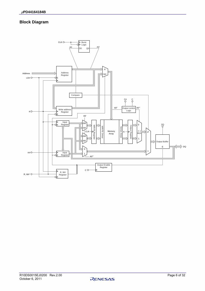
Block Diagram
2 : 1MUX
0
1
/A0'
A0'
/A0'
A0'
0
1InputRegisterE
K#
R, W#`
InputRegisterE
Write addressRegister
EK
R, W#Register
E
Output controlLogic
C# C
AddressRegister
ELD#
Address
A0'' A0'''
Compare
Output Buffer
ZQ
DQ
Output EnableRegister
C
BurstLogic
D0 Q0A0
CLK
A0'
WR
ITE
Register
MemoryArray
WR
ITE
Driver
Sense A
mps
Output R
egister
A0'
CLK K
E
A0'''
R
W#
μPD44164184B
R10DS0015EJ0200 Rev.2.00 Page 7 of 32 October 6, 2011
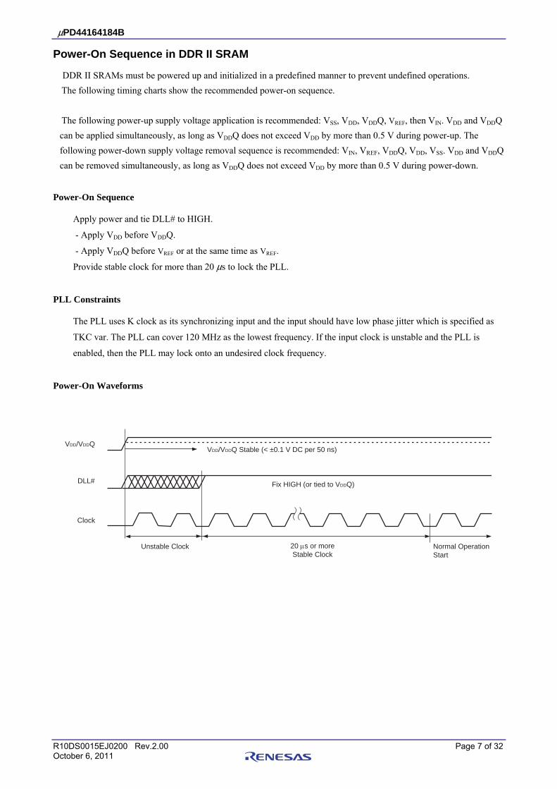
Power-On Sequence in DDR II SRAM
DDR II SRAMs must be powered up and initialized in a predefined manner to prevent undefined operations. The following timing charts show the recommended power-on sequence. The following power-up supply voltage application is recommended: VSS, VDD, VDDQ, VREF, then VIN. VDD and VDDQ can be applied simultaneously, as long as VDDQ does not exceed VDD by more than 0.5 V during power-up. The following power-down supply voltage removal sequence is recommended: VIN, VREF, VDDQ, VDD, VSS. VDD and VDDQ can be removed simultaneously, as long as VDDQ does not exceed VDD by more than 0.5 V during power-down.
Power-On Sequence
Apply power and tie DLL# to HIGH.
- Apply VDD before VDDQ.
- Apply VDDQ before VREF or at the same time as VREF.
Provide stable clock for more than 20 μs to lock the PLL.
PLL Constraints
The PLL uses K clock as its synchronizing input and the input should have low phase jitter which is specified as
TKC var. The PLL can cover 120 MHz as the lowest frequency. If the input clock is unstable and the PLL is
enabled, then the PLL may lock onto an undesired clock frequency.
Power-On Waveforms
DLL#
20 μs or moreStable Clock
VDD/VDDQ Stable (< ±0.1 V DC per 50 ns)
Fix HIGH (or tied to VDDQ)
VDD/VDDQ
Clock
Unstable Clock Normal OperationStart
μPD44164184B
R10DS0015EJ0200 Rev.2.00 Page 8 of 32 October 6, 2011
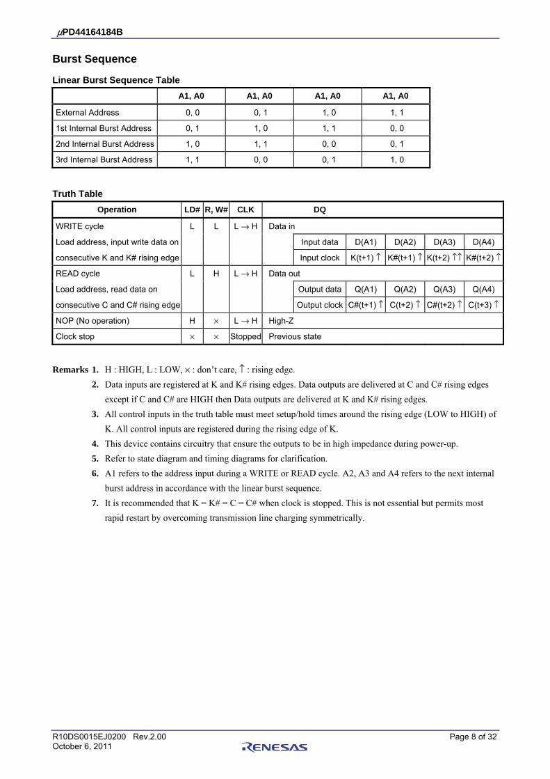
Burst Sequence
Linear Burst Sequence Table A1, A0 A1, A0 A1, A0 A1, A0
External Address 0, 0 0, 1 1, 0 1, 1
1st Internal Burst Address 0, 1 1, 0 1, 1 0, 0
2nd Internal Burst Address 1, 0 1, 1 0, 0 0, 1
3rd Internal Burst Address 1, 1 0, 0 0, 1 1, 0
Truth Table Operation LD# R, W# CLK DQ
WRITE cycle L L L → H Data in
Load address, input write data on Input data D(A1) D(A2) D(A3) D(A4)
consecutive K and K# rising edge Input clock K(t+1) ↑ K#(t+1) ↑ K(t+2) ↑↑ K#(t+2) ↑
READ cycle L H L → H Data out
Load address, read data on Output data Q(A1) Q(A2) Q(A3) Q(A4)
consecutive C and C# rising edge Output clock C#(t+1) ↑ C(t+2) ↑ C#(t+2) ↑ C(t+3) ↑
NOP (No operation) H × L → H High-Z
Clock stop × × Stopped Previous state
Remarks 1. H : HIGH, L : LOW, × : don’t care, ↑ : rising edge. 2. Data inputs are registered at K and K# rising edges. Data outputs are delivered at C and C# rising edges
except if C and C# are HIGH then Data outputs are delivered at K and K# rising edges. 3. All control inputs in the truth table must meet setup/hold times around the rising edge (LOW to HIGH) of
K. All control inputs are registered during the rising edge of K. 4. This device contains circuitry that ensure the outputs to be in high impedance during power-up. 5. Refer to state diagram and timing diagrams for clarification. 6. A1 refers to the address input during a WRITE or READ cycle. A2, A3 and A4 refers to the next internal
burst address in accordance with the linear burst sequence. 7. It is recommended that K = K# = C = C# when clock is stopped. This is not essential but permits most
rapid restart by overcoming transmission line charging symmetrically.
μPD44164184B
R10DS0015EJ0200 Rev.2.00 Page 9 of 32 October 6, 2011
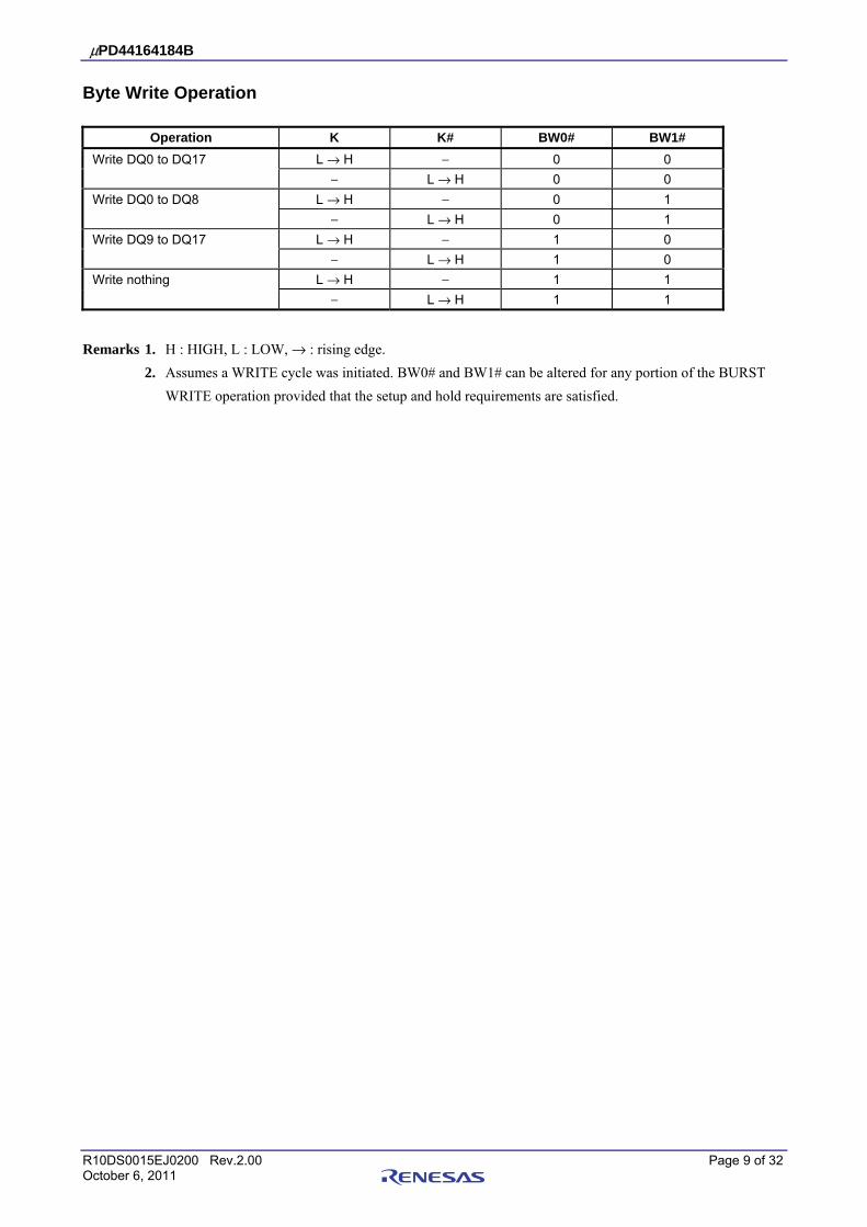
Byte Write Operation
Operation K K# BW0# BW1# Write DQ0 to DQ17 L → H − 0 0 − L → H 0 0 Write DQ0 to DQ8 L → H − 0 1 − L → H 0 1 Write DQ9 to DQ17 L → H − 1 0 − L → H 1 0 Write nothing L → H − 1 1 − L → H 1 1
Remarks 1. H : HIGH, L : LOW, → : rising edge. 2. Assumes a WRITE cycle was initiated. BW0# and BW1# can be altered for any portion of the BURST
WRITE operation provided that the setup and hold requirements are satisfied.
μPD44164184B
R10DS0015EJ0200 Rev.2.00 Page 10 of 32 October 6, 2011
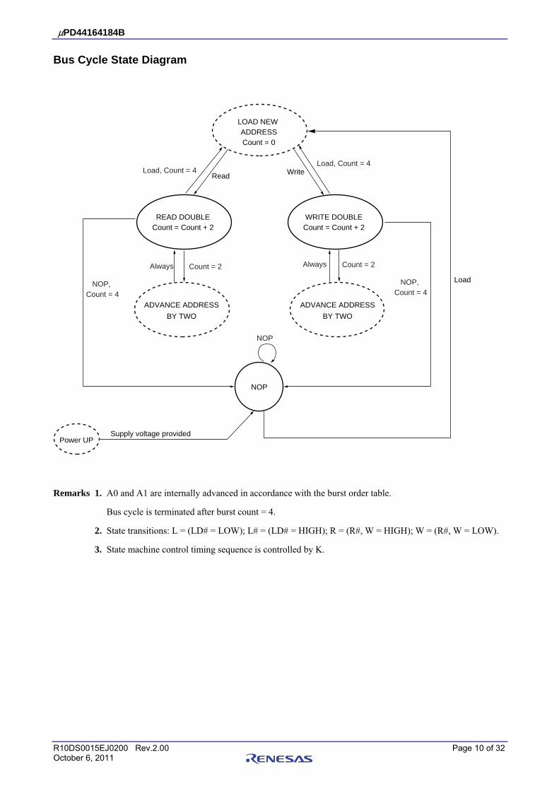
Bus Cycle State Diagram
READ DOUBLECount = Count + 2
WRITE DOUBLECount = Count + 2
Power UP
Write
NOP
Supply voltage provided
LOAD NEW ADDRESSCount = 0
NOP
ADVANCE ADDRESS
BY TWO
ADVANCE ADDRESS
BY TWO
Load, Count = 4
ReadLoad, Count = 4
Always Count = 2 Always Count = 2
LoadNOP, Count = 4
NOP, Count = 4
Remarks 1. A0 and A1 are internally advanced in accordance with the burst order table.
Bus cycle is terminated after burst count = 4.
2. State transitions: L = (LD# = LOW); L# = (LD# = HIGH); R = (R#, W = HIGH); W = (R#, W = LOW).
3. State machine control timing sequence is controlled by K.
μPD44164184B
R10DS0015EJ0200 Rev.2.00 Page 11 of 32 October 6, 2011
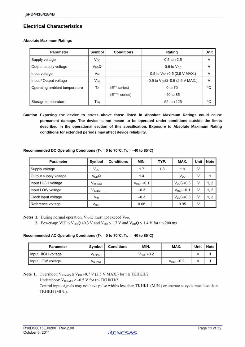
Electrical Characteristics Absolute Maximum Ratings
Parameter Symbol Conditions Rating Unit
Supply voltage VDD −0.5 to +2.5 V
Output supply voltage VDDQ −0.5 to VDD V
Input voltage VIN −0.5 to VDD+0.5 (2.5 V MAX.) V
Input / Output voltage VI/O −0.5 to VDDQ+0.5 (2.5 V MAX.) V
Operating ambient temperature TA (E** series) 0 to 70 °C
(E**Y series) −40 to 85
Storage temperature Tstg −55 to +125 °C
Caution Exposing the device to stress above those listed in Absolute Maximum Ratings could cause
permanent damage. The device is not meant to be operated under conditions outside the limits described in the operational section of this specification. Exposure to Absolute Maximum Rating conditions for extended periods may affect device reliability.
Recommended DC Operating Conditions (TA = 0 to 70°C, TA = −40 to 85°C)
Parameter Symbol Conditions MIN. TYP. MAX. Unit Note
Supply voltage VDD 1.7 1.8 1.9 V
Output supply voltage VDDQ 1.4 VDD V 1
Input HIGH voltage VIH (DC) VREF +0.1 VDDQ+0.3 V 1, 2
Input LOW voltage VIL (DC) −0.3 VREF −0.1 V 1, 2
Clock input voltage VIN −0.3 VDDQ+0.3 V 1, 2
Reference voltage VREF 0.68 0.95 V
Notes 1. During normal operation, VDDQ must not exceed VDD. 2. Power-up: VIH ≤ VDDQ +0.3 V and VDD ≤ 1.7 V and VDDQ ≤ 1.4 V for t ≤ 200 ms
Recommended AC Operating Conditions (TA = 0 to 70°C, TA = −40 to 85°C)
Parameter Symbol Conditions MIN. MAX. Unit Note
Input HIGH voltage VIH (AC) VREF +0.2 V 1
Input LOW voltage VIL (AC) VREF −0.2 V 1
Note 1. Overshoot: VIH (AC) ≤ VDD +0.7 V (2.5 V MAX.) for t ≤ TKHKH/2 Undershoot: VIL (AC) ≥ −0.5 V for t ≤ TKHKH/2 Control input signals may not have pulse widths less than TKHKL (MIN.) or operate at cycle rates less than
TKHKH (MIN.).
μPD44164184B
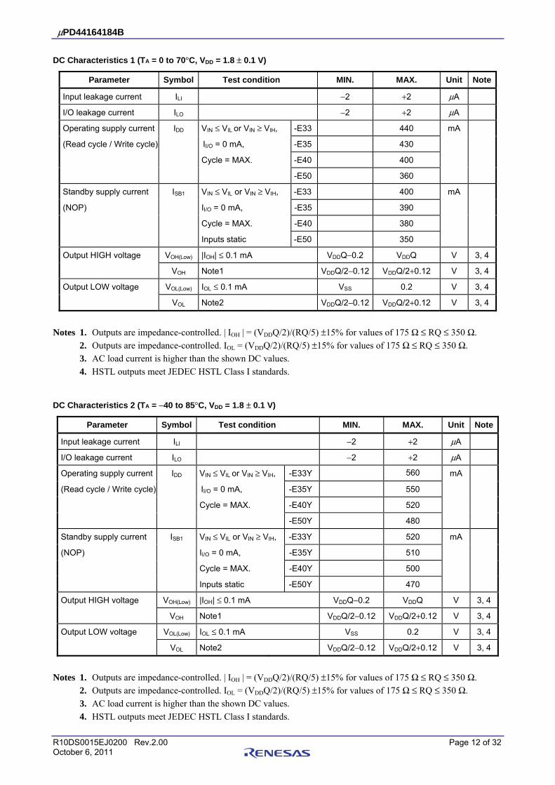
R10DS0015EJ0200 Rev.2.00 Page 12 of 32 October 6, 2011
DC Characteristics 1 (TA = 0 to 70°C, VDD = 1.8 ± 0.1 V)
Parameter Symbol Test condition MIN. MAX. Unit Note
Input leakage current ILI −2 +2 μA
I/O leakage current ILO −2 +2 μA
Operating supply current IDD VIN ≤ VIL or VIN ≥ VIH, -E33 440 mA
(Read cycle / Write cycle) II/O = 0 mA, -E35 430
Cycle = MAX. -E40 400
-E50 360
Standby supply current ISB1 VIN ≤ VIL or VIN ≥ VIH, -E33 400 mA
(NOP) II/O = 0 mA, -E35 390
Cycle = MAX. -E40 380
Inputs static -E50 350
Output HIGH voltage VOH(Low) |IOH| ≤ 0.1 mA VDDQ−0.2 VDDQ V 3, 4
VOH Note1 VDDQ/2−0.12 VDDQ/2+0.12 V 3, 4
Output LOW voltage VOL(Low) IOL ≤ 0.1 mA VSS 0.2 V 3, 4
VOL Note2 VDDQ/2−0.12 VDDQ/2+0.12 V 3, 4
Notes 1. Outputs are impedance-controlled. | IOH | = (VDDQ/2)/(RQ/5) ±15% for values of 175 Ω ≤ RQ ≤ 350 Ω. 2. Outputs are impedance-controlled. IOL = (VDDQ/2)/(RQ/5) ±15% for values of 175 Ω ≤ RQ ≤ 350 Ω. 3. AC load current is higher than the shown DC values. 4. HSTL outputs meet JEDEC HSTL Class I standards.
DC Characteristics 2 (TA = −40 to 85°C, VDD = 1.8 ± 0.1 V)
Parameter Symbol Test condition MIN. MAX. Unit Note
Input leakage current ILI −2 +2 μA
I/O leakage current ILO −2 +2 μA
Operating supply current IDD VIN ≤ VIL or VIN ≥ VIH, -E33Y 560 mA
(Read cycle / Write cycle) II/O = 0 mA, -E35Y 550
Cycle = MAX. -E40Y 520
-E50Y 480
Standby supply current ISB1 VIN ≤ VIL or VIN ≥ VIH, -E33Y 520 mA
(NOP) II/O = 0 mA, -E35Y 510
Cycle = MAX. -E40Y 500
Inputs static -E50Y 470
Output HIGH voltage VOH(Low) |IOH| ≤ 0.1 mA VDDQ−0.2 VDDQ V 3, 4
VOH Note1 VDDQ/2−0.12 VDDQ/2+0.12 V 3, 4
Output LOW voltage VOL(Low) IOL ≤ 0.1 mA VSS 0.2 V 3, 4
VOL Note2 VDDQ/2−0.12 VDDQ/2+0.12 V 3, 4
Notes 1. Outputs are impedance-controlled. | IOH | = (VDDQ/2)/(RQ/5) ±15% for values of 175 Ω ≤ RQ ≤ 350 Ω. 2. Outputs are impedance-controlled. IOL = (VDDQ/2)/(RQ/5) ±15% for values of 175 Ω ≤ RQ ≤ 350 Ω. 3. AC load current is higher than the shown DC values. 4. HSTL outputs meet JEDEC HSTL Class I standards.
μPD44164184B
R10DS0015EJ0200 Rev.2.00 Page 13 of 32 October 6, 2011
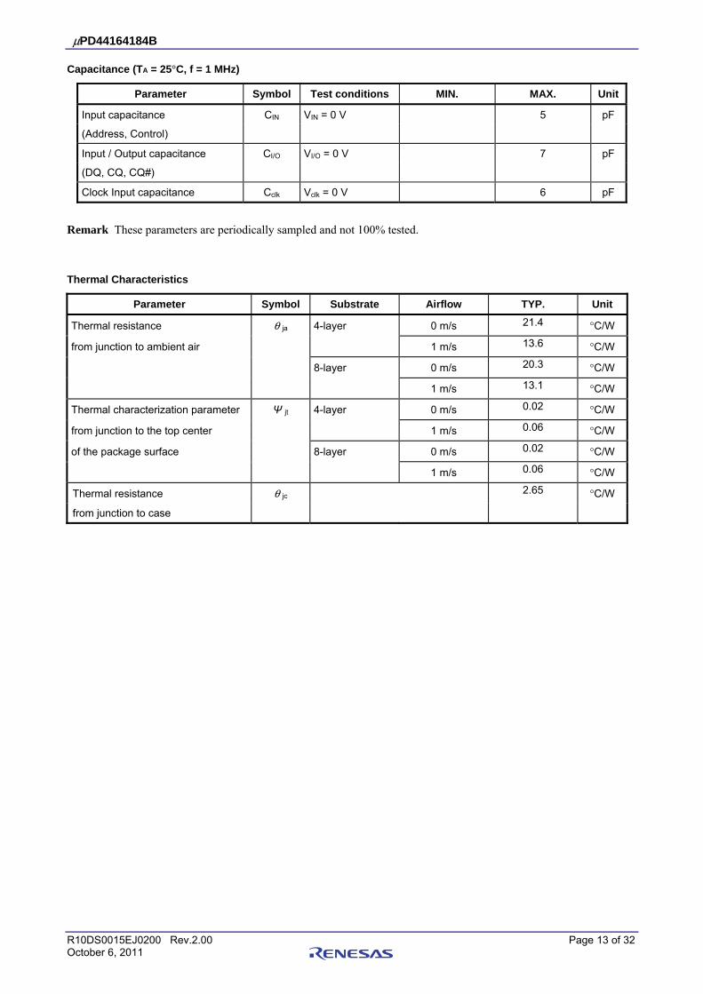
Capacitance (TA = 25°C, f = 1 MHz)
Parameter Symbol Test conditions MIN. MAX. Unit
Input capacitance CIN VIN = 0 V 5 pF
(Address, Control)
Input / Output capacitance CI/O VI/O = 0 V 7 pF
(DQ, CQ, CQ#)
Clock Input capacitance Cclk Vclk = 0 V 6 pF
Remark These parameters are periodically sampled and not 100% tested.
Thermal Characteristics
Parameter Symbol Substrate Airflow TYP. Unit
Thermal resistance θ ja 4-layer 0 m/s 21.4 °C/W
from junction to ambient air 1 m/s 13.6 °C/W
8-layer 0 m/s 20.3 °C/W
1 m/s 13.1 °C/W
Thermal characterization parameter Ψ jt 4-layer 0 m/s 0.02 °C/W
from junction to the top center 1 m/s 0.06 °C/W
of the package surface 8-layer 0 m/s 0.02 °C/W
1 m/s 0.06 °C/W
Thermal resistance θ jc 2.65 °C/W
from junction to case
μPD44164184B
R10DS0015EJ0200 Rev.2.00 Page 14 of 32 October 6, 2011
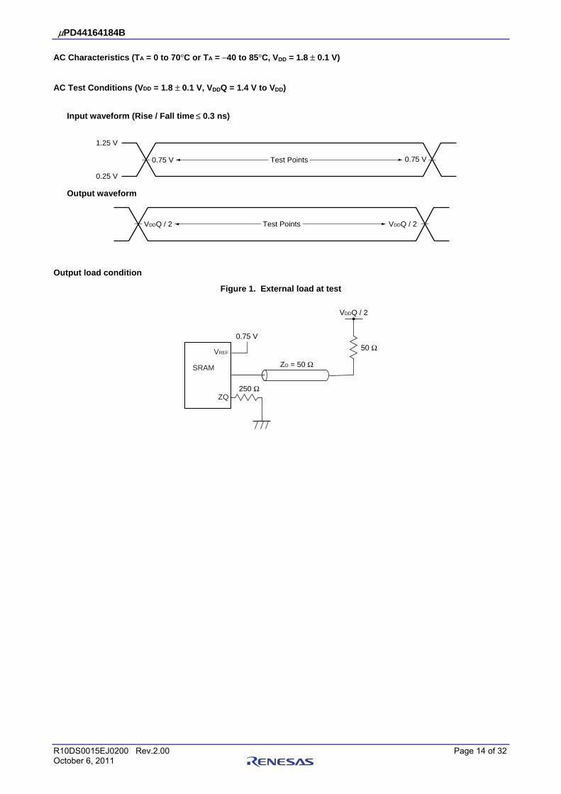
AC Characteristics (TA = 0 to 70°C or TA = −40 to 85°C, VDD = 1.8 ± 0.1 V)
AC Test Conditions (VDD = 1.8 ± 0.1 V, VDDQ = 1.4 V to VDD)
Input waveform (Rise / Fall time ≤ 0.3 ns)
0.75 V 0.75 VTest Points
1.25 V
0.25 V
Output waveform
VDDQ / 2 VDDQ / 2Test Points
Output load condition
Figure 1. External load at test
VDDQ / 2
0.75 V
50 Ω
ZO = 50 Ω
250 Ω
SRAM
VREF
ZQ
μPD44164184B
R10DS0015EJ0200 Rev.2.00 Page 15 of 32 October 6, 2011
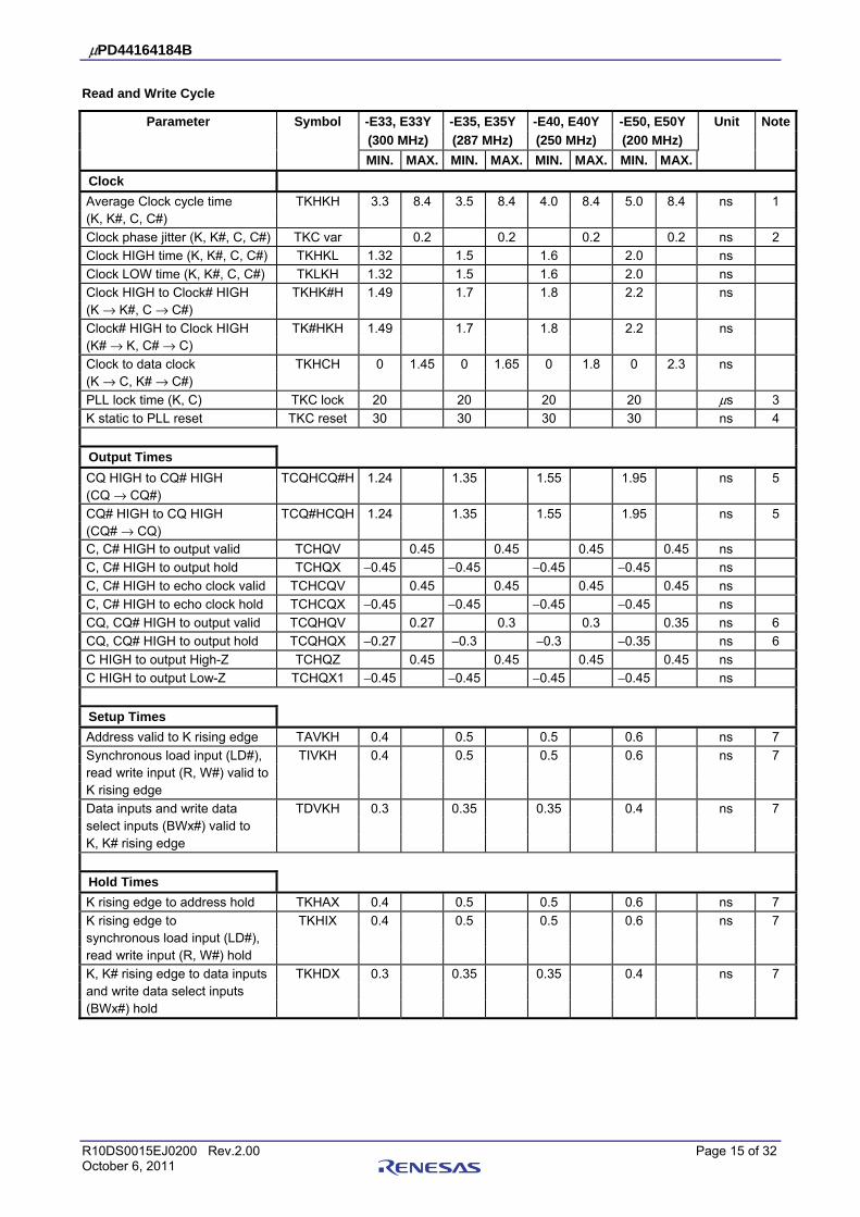
Read and Write Cycle
Parameter Symbol -E33, E33Y -E35, E35Y -E40, E40Y -E50, E50Y Unit Note (300 MHz) (287 MHz) (250 MHz) (200 MHz) MIN. MAX. MIN. MAX. MIN. MAX. MIN. MAX.
Clock Average Clock cycle time TKHKH 3.3 8.4 3.5 8.4 4.0 8.4 5.0 8.4 ns 1 (K, K#, C, C#) Clock phase jitter (K, K#, C, C#) TKC var 0.2 0.2 0.2 0.2 ns 2 Clock HIGH time (K, K#, C, C#) TKHKL 1.32 1.5 1.6 2.0 ns Clock LOW time (K, K#, C, C#) TKLKH 1.32 1.5 1.6 2.0 ns Clock HIGH to Clock# HIGH TKHK#H 1.49 1.7 1.8 2.2 ns (K → K#, C → C#) Clock# HIGH to Clock HIGH TK#HKH 1.49 1.7 1.8 2.2 ns (K# → K, C# → C) Clock to data clock TKHCH 0 1.45 0 1.65 0 1.8 0 2.3 ns (K → C, K# → C#) PLL lock time (K, C) TKC lock 20 20 20 20 μs 3 K static to PLL reset TKC reset 30 30 30 30 ns 4 Output Times CQ HIGH to CQ# HIGH TCQHCQ#H 1.24 1.35 1.55 1.95 ns 5 (CQ → CQ#) CQ# HIGH to CQ HIGH TCQ#HCQH 1.24 1.35 1.55 1.95 ns 5 (CQ# → CQ) C, C# HIGH to output valid TCHQV 0.45 0.45 0.45 0.45 ns C, C# HIGH to output hold TCHQX −0.45 −0.45 −0.45 −0.45 ns C, C# HIGH to echo clock valid TCHCQV 0.45 0.45 0.45 0.45 ns C, C# HIGH to echo clock hold TCHCQX −0.45 −0.45 −0.45 −0.45 ns CQ, CQ# HIGH to output valid TCQHQV 0.27 0.3 0.3 0.35 ns 6 CQ, CQ# HIGH to output hold TCQHQX −0.27 −0.3 −0.3 −0.35 ns 6 C HIGH to output High-Z TCHQZ 0.45 0.45 0.45 0.45 ns C HIGH to output Low-Z TCHQX1 −0.45 −0.45 −0.45 −0.45 ns
Setup Times Address valid to K rising edge TAVKH 0.4 0.5 0.5 0.6 ns 7 Synchronous load input (LD#), TIVKH 0.4 0.5 0.5 0.6 ns 7 read write input (R, W#) valid to K rising edge Data inputs and write data TDVKH 0.3 0.35 0.35 0.4 ns 7 select inputs (BWx#) valid to K, K# rising edge
Hold Times K rising edge to address hold TKHAX 0.4 0.5 0.5 0.6 ns 7 K rising edge to TKHIX 0.4 0.5 0.5 0.6 ns 7 synchronous load input (LD#), read write input (R, W#) hold K, K# rising edge to data inputs TKHDX 0.3 0.35 0.35 0.4 ns 7 and write data select inputs (BWx#) hold
μPD44164184B
R10DS0015EJ0200 Rev.2.00 Page 16 of 32 October 6, 2011
Notes 1. When debugging the system or board, these products can operate at a clock frequency slower than TKHKH (MAX.) without the PLL circuit being used, if DLL# = LOW. Read latency (RL) is changed to 1.0 clock cycle in this operation. The AC/DC characteristics cannot be guaranteed, however.
2. Clock phase jitter is the variance from clock rising edge to the next expected clock rising edge. TKC var (MAX.) indicates a peak-to-peak value.
3. VDD slew rate must be less than 0.1 V DC per 50 ns for PLL lock retention. PLL lock time begins once VDD and input clock are stable. It is recommended that the device is kept NOP (LD# = HIGH) during these cycles.
4. K input is monitored for this operation. See below for the timing.
K
K
TKC resetor
TKC reset
5. Guaranteed by design. 6. Echo clock is very tightly controlled to data valid / data hold. By design, there is a ± 0.1 ns variation from
echo clock to data. The data sheet parameters reflect tester guardbands and test setup variations. 7. This is a synchronous device. All addresses, data and control lines must meet the specified setup and hold
times for all latching clock edges. Remarks 1. This parameter is sampled. 2. Test conditions as specified with the output loading as shown in AC Test Conditions unless otherwise
noted. 3. Control input signals may not be operated with pulse widths less than TKHKL (MIN.). 4. If C, C# are tied HIGH, K, K# become the references for C, C# timing parameters. 5. VDDQ is 1.5 V DC.
μPD44164184B
R10DS0015EJ0200 Rev.2.00 Page 17 of 32 October 6, 2011
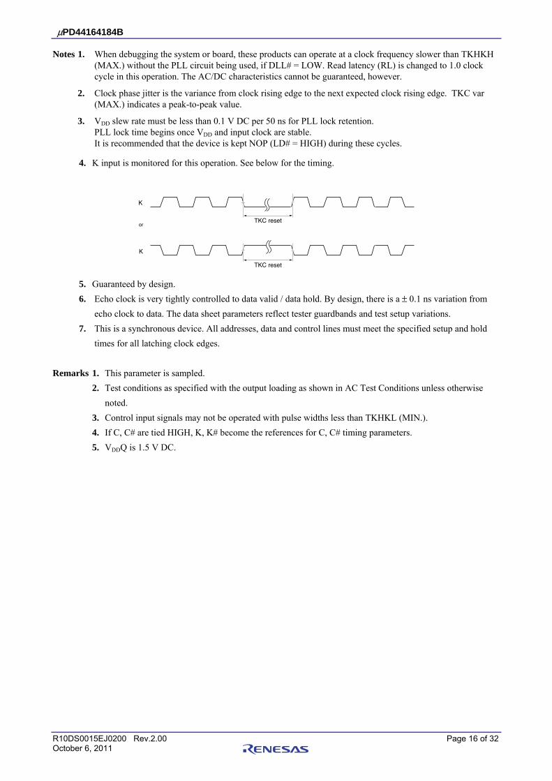
Read and Write Timing
TKHKH
TKHAX
Q00 Q02
K
LD#
Address
DQ Q01
K#
2 4 6 8 10 12 131 3 5 7 9 11
R, W#
Qx2 Q03 Q11Q10 Q13Q12 D20 D22D21 D23 D31D30 D33D32
TKHK#H TK#HKH
CQ
CQ#
C
C#
TKHCH
TCHQX1
TCHQVTCHQV
TCHQXTCHQX
TCQHQX
TCQHQVTCHQZ
TKHKL TKLKH TKHK#H
TDVKH
TKHDX
TDVKH
TKHDX
NOP READ(burst of 4)
READ(burst of 4)
NOP NOP WRITE(burst of 4)
WRITE(burst of 4)
READ(burst of 4)
TKHKL TKLKH
TKHIX
TKLKH
TCHCQV
TCHCQV
TCHCQX
TCHCQX
A0 A1 A2 A4A3
TK#HKH
TIVKH
TAVKH
TKHCH
TKHKH
TCQ#HCQHTCQHCQ#H
Remarks 1. Q01 refers to output from address A0. Q02 refers to output from the next internal burst address following A0, etc.
2. Outputs are disabled (high impedance) 3.5 clock cycles after the last READ (LD# = LOW, R, W# = HIGH) is input in the sequences of [READ]-[NOP].
3. The second NOP cycle at the cycle “7” is not necessary for correct device operation; however, at high clock frequencies it may be required to prevent bus contention.
μPD44164184B
R10DS0015EJ0200 Rev.2.00 Page 18 of 32 October 6, 2011
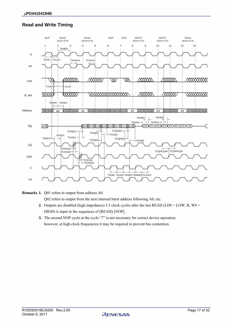
Application Example
SRAMController
Data IO
Address
LD#
R, W#
BW#
SRAM#1 CQ/CQ#
SRAM#4 CQ/CQ#
Source CLK/CLK#
Return CLK/CLK#
ZQCQ#
CQSRAM#4DQ
A LD# R, W# BWx# C/C# K/K#
R
RVt
Vt
RVt
RVt
RVt
R =250 Ω
R =250 Ω
ZQCQ#
CQSRAM#1DQ
A LD# R, W# BWx# C/C# K/K#
R = 50 Ω Vt = Vref
. . .
. . .
Remark AC characteristics are defined at the condition of SRAM outputs, CQ, CQ# and DQ with termination.
μPD44164184B
R10DS0015EJ0200 Rev.2.00 Page 19 of 32 October 6, 2011
JTAG Specification
These products support a limited set of JTAG functions as in IEEE standard 1149.1.
Test Access Port (TAP) Pins Pin name Pin assignments Description
TCK 2R Test Clock Input. All input are captured on the rising edge of TCK and all outputs propagate from the falling edge of TCK.
TMS 10R Test Mode Select. This is the command input for the TAP controller state machine.
TDI 11R Test Data Input. This is the input side of the serial registers placed between TDI and TDO. The register placed between TDI and TDO is determined by the state of the TAP controller state machine and the instruction that is currently loaded in the TAP instruction.
TDO 1R Test Data Output. This is the output side of the serial registers placed between TDI and TDO. Output changes in response to the falling edge of TCK.
Remark The device does not have TRST (TAP reset). The Test-Logic Reset state is entered while TMS is held HIGH
for five rising edges of TCK. The TAP controller state is also reset on the SRAM POWER-UP.
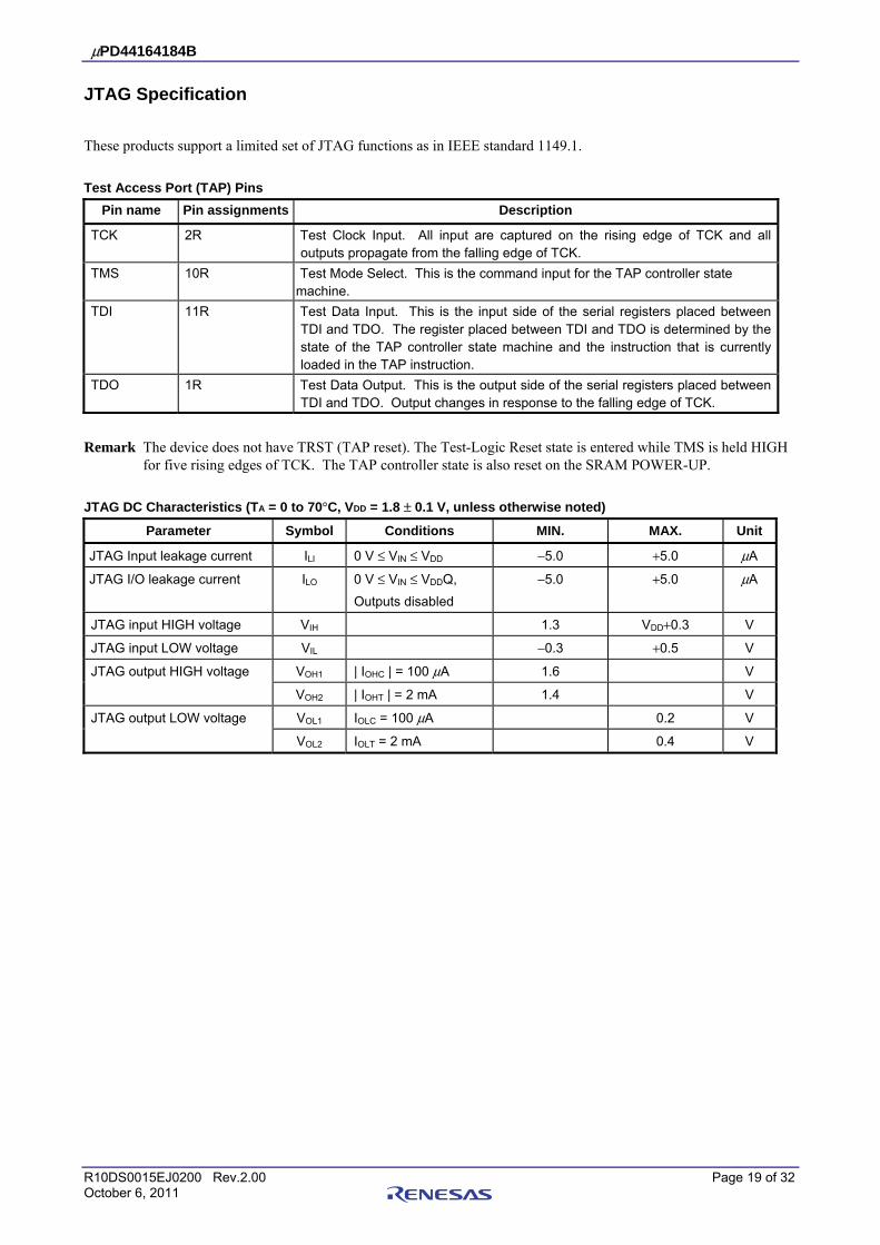
JTAG DC Characteristics (TA = 0 to 70°C, VDD = 1.8 ± 0.1 V, unless otherwise noted)
Parameter Symbol Conditions MIN. MAX. Unit
JTAG Input leakage current ILI 0 V ≤ VIN ≤ VDD −5.0 +5.0 μA
JTAG I/O leakage current ILO 0 V ≤ VIN ≤ VDDQ, −5.0 +5.0 μA
Outputs disabled
JTAG input HIGH voltage VIH 1.3 VDD+0.3 V
JTAG input LOW voltage VIL −0.3 +0.5 V
JTAG output HIGH voltage VOH1 | IOHC | = 100 μA 1.6 V
VOH2 | IOHT | = 2 mA 1.4 V
JTAG output LOW voltage VOL1 IOLC = 100 μA 0.2 V
VOL2 IOLT = 2 mA 0.4 V
μPD44164184B
R10DS0015EJ0200 Rev.2.00 Page 20 of 32 October 6, 2011
JTAG AC Test Conditions
Input waveform (Rise / Fall time ≤ 1 ns)
0.9 V 0.9 VTest Points
1.8 V
0 V
Output waveform
0.9 V 0.9 VTest Points
Output load
Figure 2. External load at test
TDO
ZO = 50 Ω
VTT = 0.9 V
20 pF
50 Ω
μPD44164184B
R10DS0015EJ0200 Rev.2.00 Page 21 of 32 October 6, 2011
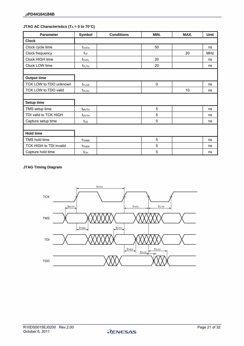
JTAG AC Characteristics (TA = 0 to 70°C)
Parameter Symbol Conditions MIN. MAX. UnitClock Clock cycle time tTHTH 50 ns Clock frequency fTF 20 MHz
Clock HIGH time tTHTL 20 ns
Clock LOW time tTLTH 20 ns
Output time TCK LOW to TDO unknown tTLOX 0 ns TCK LOW to TDO valid tTLOV 10 ns
Setup time TMS setup time tMVTH 5 ns TDI valid to TCK HIGH tDVTH 5 ns
Capture setup time tCS 5 ns
Hold time TMS hold time tTHMX 5 ns TCK HIGH to TDI invalid tTHDX 5 ns
Capture hold time tCH 5 ns
JTAG Timing Diagram
tTHTH
tTLOV
tTLTHtTHTLtMVTH
tTHDX
tDVTHtTHMX
TCK
TMS
TDI
TDO
tTLOX
μPD44164184B
R10DS0015EJ0200 Rev.2.00 Page 22 of 32 October 6, 2011
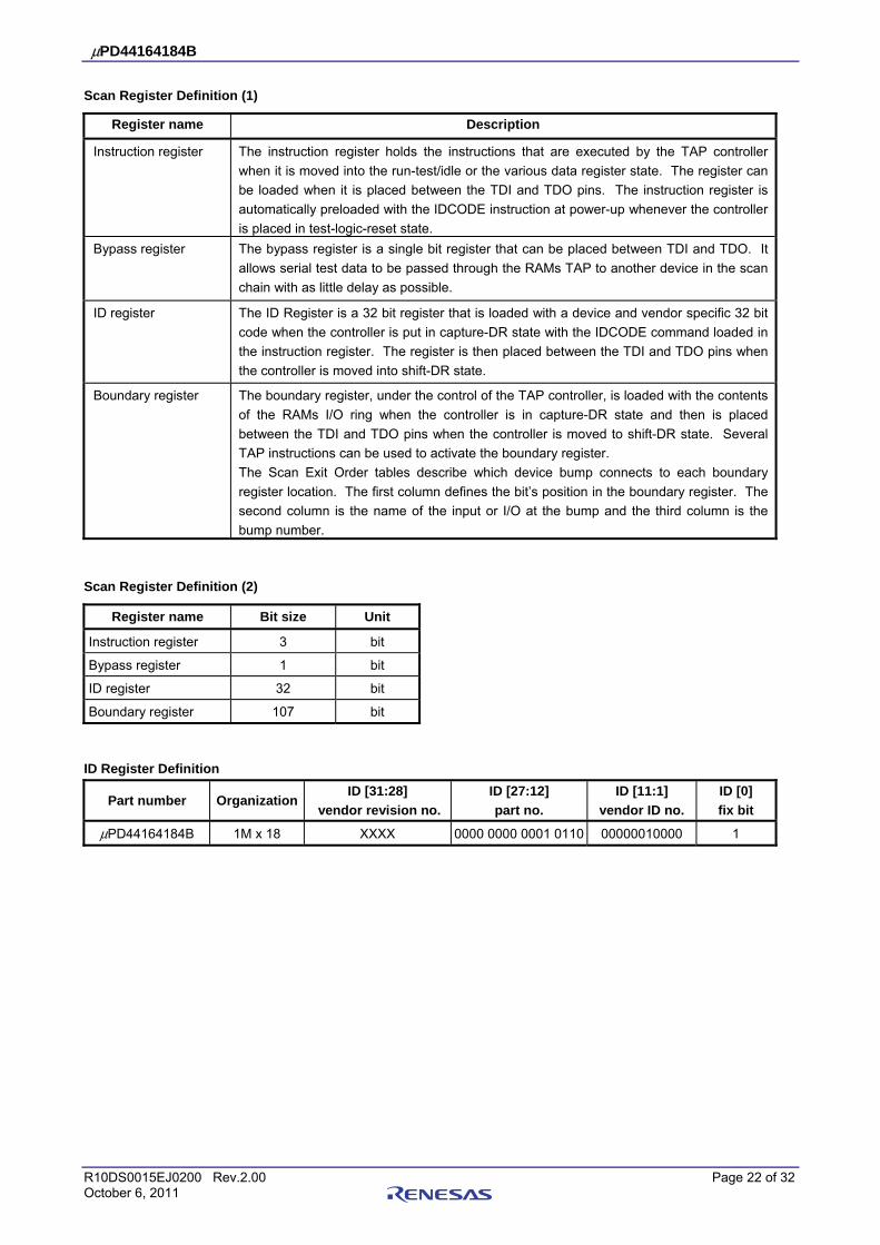
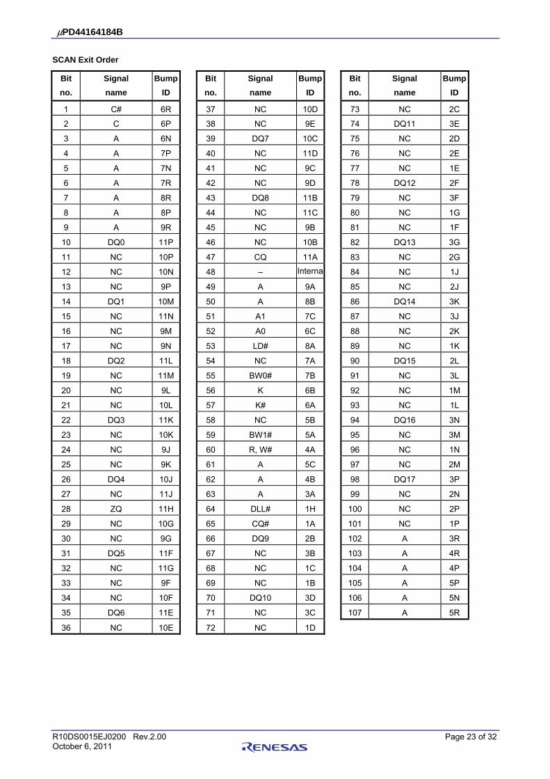
Scan Register Definition (1)
Register name Description
Instruction register The instruction register holds the instructions that are executed by the TAP controller when it is moved into the run-test/idle or the various data register state. The register can be loaded when it is placed between the TDI and TDO pins. The instruction register is automatically preloaded with the IDCODE instruction at power-up whenever the controller is placed in test-logic-reset state.
Bypass register The bypass register is a single bit register that can be placed between TDI and TDO. It allows serial test data to be passed through the RAMs TAP to another device in the scan chain with as little delay as possible.
ID register The ID Register is a 32 bit register that is loaded with a device and vendor specific 32 bit code when the controller is put in capture-DR state with the IDCODE command loaded in the instruction register. The register is then placed between the TDI and TDO pins when the controller is moved into shift-DR state.
Boundary register The boundary register, under the control of the TAP controller, is loaded with the contents of the RAMs I/O ring when the controller is in capture-DR state and then is placed between the TDI and TDO pins when the controller is moved to shift-DR state. Several TAP instructions can be used to activate the boundary register. The Scan Exit Order tables describe which device bump connects to each boundary register location. The first column defines the bit’s position in the boundary register. The second column is the name of the input or I/O at the bump and the third column is the bump number.
Scan Register Definition (2)
Register name Bit size Unit
Instruction register 3 bit
Bypass register 1 bit
ID register 32 bit
Boundary register 107 bit
ID Register Definition
Part number Organization ID [31:28]
vendor revision no.ID [27:12] part no.
ID [11:1] vendor ID no.
ID [0] fix bit
μPD44164184B 1M x 18 XXXX 0000 0000 0001 0110 00000010000 1
μPD44164184B
R10DS0015EJ0200 Rev.2.00 Page 23 of 32 October 6, 2011
SCAN Exit Order
Bit Signal Bump Bit Signal Bump Bit Signal Bumpno. name ID no. name ID no. name ID
1 C# 6R 37 NC 10D 73 NC 2C
2 C 6P 38 NC 9E 74 DQ11 3E
3 A 6N 39 DQ7 10C 75 NC 2D
4 A 7P 40 NC 11D 76 NC 2E
5 A 7N 41 NC 9C 77 NC 1E
6 A 7R 42 NC 9D 78 DQ12 2F
7 A 8R 43 DQ8 11B 79 NC 3F
8 A 8P 44 NC 11C 80 NC 1G
9 A 9R 45 NC 9B 81 NC 1F
10 DQ0 11P 46 NC 10B 82 DQ13 3G
11 NC 10P 47 CQ 11A 83 NC 2G
12 NC 10N 48 – Interna 84 NC 1J
13 NC 9P 49 A 9A 85 NC 2J
14 DQ1 10M 50 A 8B 86 DQ14 3K
15 NC 11N 51 A1 7C 87 NC 3J
16 NC 9M 52 A0 6C 88 NC 2K
17 NC 9N 53 LD# 8A 89 NC 1K
18 DQ2 11L 54 NC 7A 90 DQ15 2L
19 NC 11M 55 BW0# 7B 91 NC 3L
20 NC 9L 56 K 6B 92 NC 1M
21 NC 10L 57 K# 6A 93 NC 1L
22 DQ3 11K 58 NC 5B 94 DQ16 3N
23 NC 10K 59 BW1# 5A 95 NC 3M
24 NC 9J 60 R, W# 4A 96 NC 1N
25 NC 9K 61 A 5C 97 NC 2M
26 DQ4 10J 62 A 4B 98 DQ17 3P
27 NC 11J 63 A 3A 99 NC 2N
28 ZQ 11H 64 DLL# 1H 100 NC 2P
29 NC 10G 65 CQ# 1A 101 NC 1P
30 NC 9G 66 DQ9 2B 102 A 3R
31 DQ5 11F 67 NC 3B 103 A 4R
32 NC 11G 68 NC 1C 104 A 4P
33 NC 9F 69 NC 1B 105 A 5P
34 NC 10F 70 DQ10 3D 106 A 5N
35 DQ6 11E 71 NC 3C 107 A 5R
36 NC 10E 72 NC 1D
μPD44164184B
R10DS0015EJ0200 Rev.2.00 Page 24 of 32 October 6, 2011
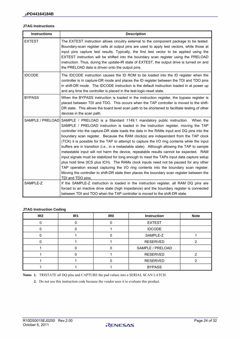
JTAG Instructions
Instructions Description
EXTEST The EXTEST instruction allows circuitry external to the component package to be tested. Boundary-scan register cells at output pins are used to apply test vectors, while those at input pins capture test results. Typically, the first test vector to be applied using the EXTEST instruction will be shifted into the boundary scan register using the PRELOAD instruction. Thus, during the update-IR state of EXTEST, the output drive is turned on and the PRELOAD data is driven onto the output pins.
IDCODE The IDCODE instruction causes the ID ROM to be loaded into the ID register when the controller is in capture-DR mode and places the ID register between the TDI and TDO pins in shift-DR mode. The IDCODE instruction is the default instruction loaded in at power up and any time the controller is placed in the test-logic-reset state.
BYPASS When the BYPASS instruction is loaded in the instruction register, the bypass register is placed between TDI and TDO. This occurs when the TAP controller is moved to the shift-DR state. This allows the board level scan path to be shortened to facilitate testing of other devices in the scan path.
SAMPLE / PRELOAD SAMPLE / PRELOAD is a Standard 1149.1 mandatory public instruction. When the SAMPLE / PRELOAD instruction is loaded in the instruction register, moving the TAP controller into the capture-DR state loads the data in the RAMs input and DQ pins into the boundary scan register. Because the RAM clock(s) are independent from the TAP clock (TCK) it is possible for the TAP to attempt to capture the I/O ring contents while the input buffers are in transition (i.e., in a metastable state). Although allowing the TAP to sample metastable input will not harm the device, repeatable results cannot be expected. RAM input signals must be stabilized for long enough to meet the TAPs input data capture setup plus hold time (tCS plus tCH). The RAMs clock inputs need not be paused for any other TAP operation except capturing the I/O ring contents into the boundary scan register. Moving the controller to shift-DR state then places the boundary scan register between the TDI and TDO pins.
SAMPLE-Z If the SAMPLE-Z instruction is loaded in the instruction register, all RAM DQ pins are forced to an inactive drive state (high impedance) and the boundary register is connected between TDI and TDO when the TAP controller is moved to the shift-DR state.
JTAG Instruction Coding
IR2 IR1 IR0 Instruction Note
0 0 0 EXTEST
0 0 1 IDCODE
0 1 0 SAMPLE-Z 1
0 1 1 RESERVED 2
1 0 0 SAMPLE / PRELOAD
1 0 1 RESERVED 2
1 1 0 RESERVED 2
1 1 1 BYPASS
Notes 1. TRISTATE all DQ pins and CAPTURE the pad values into a SERIAL SCAN LATCH.
2. Do not use this instruction code because the vendor uses it to evaluate this product.
μPD44164184B
R10DS0015EJ0200 Rev.2.00 Page 25 of 32 October 6, 2011
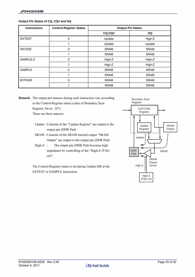
Output Pin States of CQ, CQ# and DQ
Instructions Control-Register Status Output Pin Status
CQ,CQ# DQ
EXTEST 0 Update High-Z
1 Update Update
IDCODE 0 SRAM SRAM
1 SRAM SRAM
SAMPLE-Z 0 High-Z High-Z
1 High-Z High-Z
SAMPLE 0 SRAM SRAM
1 SRAM SRAM
BYPASS 0 SRAM SRAM
1 SRAM SRAM
Remark The output pin statuses during each instruction vary according to the Control-Register status (value of Boundary Scan Register, bit no. 107). There are three statuses:
Update : Contents of the “Update Register” are output to the output pin (DDR Pad).
SRAM : Contents of the SRAM internal output “SRAM Output” are output to the output pin (DDR Pad).
High-Z : The output pin (DDR Pad) becomes high impedance by controlling of the “High-Z JTAG ctrl”.
The Control-Register status is set during Update-DR at the EXTEST or SAMPLE instruction.
SRAM
CAPTURERegister
Boundary Scan Register
UpdateRegister
DDRPad
SRAMOutputDriver
High-ZJTAG ctrl
High-Z
Update
SRAMOutput
μPD44164184B
R10DS0015EJ0200 Rev.2.00 Page 26 of 32 October 6, 2011
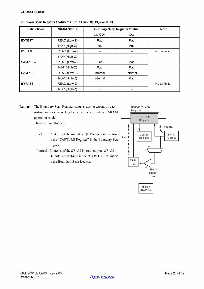
Boundary Scan Register Status of Output Pins CQ, CQ# and DQ
Instructions SRAM Status Boundary Scan Register Status Note
CQ,CQ# DQ
EXTEST READ (Low-Z) Pad Pad
NOP (High-Z) Pad Pad
IDCODE READ (Low-Z) − − No definition
NOP (High-Z) − −
SAMPLE-Z READ (Low-Z) Pad Pad
NOP (High-Z) Pad Pad
SAMPLE READ (Low-Z) Internal Internal
NOP (High-Z) Internal Pad
BYPASS READ (Low-Z) − − No definition
NOP (High-Z) − −
Remark The Boundary Scan Register statuses during execution each instruction vary according to the instruction code and SRAM operation mode. There are two statuses:
Pad : Contents of the output pin (DDR Pad) are captured in the “CAPTURE Register” in the Boundary Scan Register.
Internal : Contents of the SRAM internal output “SRAM Output” are captured in the “CAPTURE Register” in the Boundary Scan Register.
Pad
Internal
SRAMOutputDriver
UpdateRegister
DDRPad
High-ZJTAG ctrl
CAPTURERegister
SRAMOutput
Boundary Scan Register
μPD44164184B
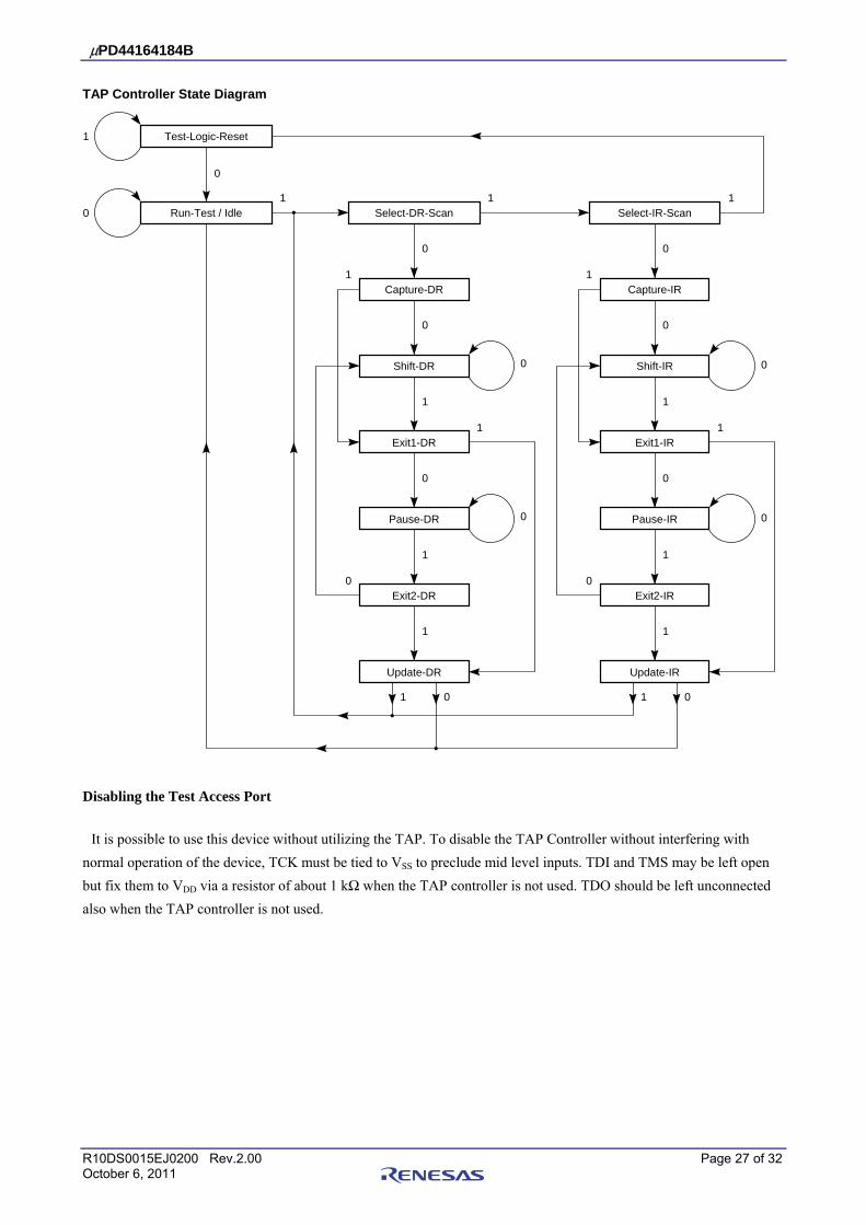
R10DS0015EJ0200 Rev.2.00 Page 27 of 32 October 6, 2011
TAP Controller State Diagram
Test-Logic-Reset
Run-Test / Idle Select-DR-Scan
Capture-DR Capture-IR
Shift-DR
Exit1-DR
Pause-DR
Exit2-DR
Update-DR Update-IR
Exit2-IR
Pause-IR
Exit1-IR
Shift-IR
Select-IR-Scan
0
0
0
1
0
1
1
0
0
1
0
1
1
0
0
0
0
1 0 1 0
1 1 10
1
1
0
1
0
1 1
Disabling the Test Access Port
It is possible to use this device without utilizing the TAP. To disable the TAP Controller without interfering with normal operation of the device, TCK must be tied to VSS to preclude mid level inputs. TDI and TMS may be left open but fix them to VDD via a resistor of about 1 kΩ when the TAP controller is not used. TDO should be left unconnected also when the TAP controller is not used.
μPD44164184B
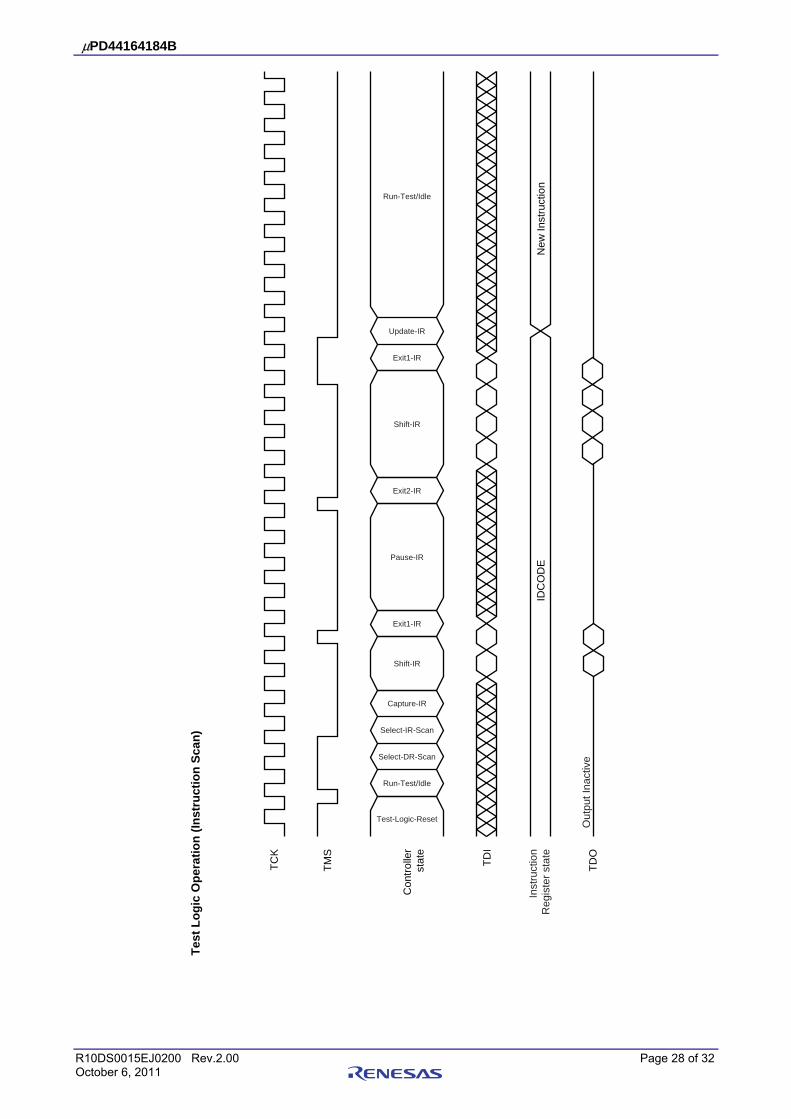
R10DS0015EJ0200 Rev.2.00 Page 28 of 32 October 6, 2011
Test
Log
ic O
pera
tion
(Inst
ruct
ion
Scan
)
TCK
Con
trolle
rst
ate
TDI
TMS
TDO
Test-Logic-Reset
Run-Test/Idle
Select-DR-Scan
Select-IR-Scan
Capture-IR
Shift-IR
Exit1-IR
Pause-IR
Exit2-IR
Shift-IR
Exit1-IR
Update-IR
Run-Test/Idle
IDC
OD
EIn
stru
ctio
nR
egis
ter s
tate
New
Inst
ruct
ion
Out
put I
nact
ive
μPD44164184B
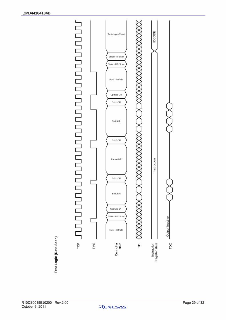
R10DS0015EJ0200 Rev.2.00 Page 29 of 32 October 6, 2011
Test
Log
ic (D
ata
Scan
)
Con
trolle
rst
ate
TDI
TMS
TDO
Run-Test/Idle
Select-DR-Scan
Capture-DR
Shift-DR
Exit1-DR
Pause-DR
Exit2-DR
Shift-DR
Exit1-DR
Update-DR
Test-Logic-Reset
Inst
ruct
ion
Inst
ruct
ion
Reg
iste
r sta
teID
CO
DE
Run-Test/Idle
Select-DR-Scan
Select-IR-Scan
Out
put I
nact
ive
TCK
μPD44164184B
R10DS0015EJ0200 Rev.2.00 Page 30 of 32 October 6, 2011
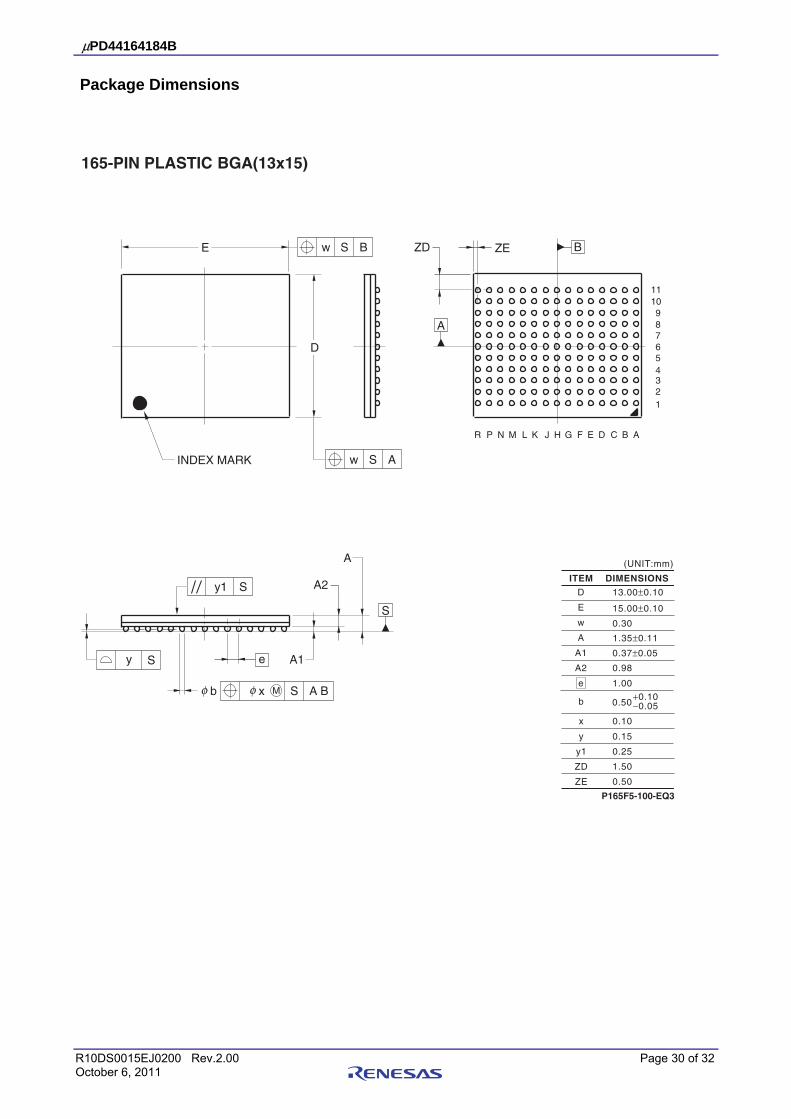
Package Dimensions
165-PIN PLASTIC BGA(13x15)
ITEM DIMENSIONS
D
E
w
A
A1
A2
e
13.00±0.10
15.00±0.10
0.30
0.37±0.05
−0.05
0.10
1.35±0.11
0.98
1.00
(UNIT:mm)
0.15
0.25
1.50
0.50
S
e
y1 S
A
A1
A2
Sy
Sxb A BM
Sw A
Sw B ZEZD
INDEX MARK
A
B
123456789
1011
ABCDEFGHJKLMNPR
E
D
x
y
y1
ZD
ZE
b 0.50
P165F5-100-EQ3
+0.10
μPD44164184B
R10DS0015EJ0200 Rev.2.00 Page 31 of 32 October 6, 2011
Recommended Soldering Condition
Please consult with our sales offices for soldering conditions of these products.
Types of Surface Mount Devices
μPD44164184BF5-EQ3 : 165-pin PLASTIC BGA (13 x 15)
Quality Grade
• A quality grade of the products is “Standard”. • Anti-radioactive design is not implemented in the products. • Semiconductor devices have the possibility of unexpected defects by affection of cosmic ray that reach to
the ground and so forth.
All trademarks and registered trademarks are the property of their respective owners.
C - 32
Revision History μPD44164184B
Description Rev. Date
Page Summary 1st edition ’10.02.01 - New Preliminary Data Sheet Rev.0.02 ’10.08.18 P12 DC Characteristics (Modification, Spec of IDD and ISB1) P13 Thermal Characteristics (Modification, Spec) Rev.1.00 ’11.01.05 P29 Package Dimensions (Modification, Dimensions) Throughout Preliminary Data Sheet Data Sheet Rev.2.00 ’11.10.06 Throughout Add Lead and the extended temperature operation product
Notice1. All information included in this document is current as of the date this document is issued. Such information, however, is subject to change without any prior notice. Before purchasing or using any Renesas
Electronics products listed herein, please confirm the latest product information with a Renesas Electronics sales office. Also, please pay regular and careful attention to additional and different information to
be disclosed by Renesas Electronics such as that disclosed through our website.
2. Renesas Electronics does not assume any liability for infringement of patents, copyrights, or other intellectual property rights of third parties by or arising from the use of Renesas Electronics products or
technical information described in this document. No license, express, implied or otherwise, is granted hereby under any patents, copyrights or other intellectual property rights of Renesas Electronics or
others.
3. You should not alter, modify, copy, or otherwise misappropriate any Renesas Electronics product, whether in whole or in part.
4. Descriptions of circuits, software and other related information in this document are provided only to illustrate the operation of semiconductor products and application examples. You are fully responsible for
the incorporation of these circuits, software, and information in the design of your equipment. Renesas Electronics assumes no responsibility for any losses incurred by you or third parties arising from the
use of these circuits, software, or information.
5. When exporting the products or technology described in this document, you should comply with the applicable export control laws and regulations and follow the procedures required by such laws and
regulations. You should not use Renesas Electronics products or the technology described in this document for any purpose relating to military applications or use by the military, including but not limited to
the development of weapons of mass destruction. Renesas Electronics products and technology may not be used for or incorporated into any products or systems whose manufacture, use, or sale is
prohibited under any applicable domestic or foreign laws or regulations.
6. Renesas Electronics has used reasonable care in preparing the information included in this document, but Renesas Electronics does not warrant that such information is error free. Renesas Electronics
assumes no liability whatsoever for any damages incurred by you resulting from errors in or omissions from the information included herein.
7. Renesas Electronics products are classified according to the following three quality grades: "Standard", "High Quality", and "Specific". The recommended applications for each Renesas Electronics product
depends on the product's quality grade, as indicated below. You must check the quality grade of each Renesas Electronics product before using it in a particular application. You may not use any Renesas
Electronics product for any application categorized as "Specific" without the prior written consent of Renesas Electronics. Further, you may not use any Renesas Electronics product for any application for
which it is not intended without the prior written consent of Renesas Electronics. Renesas Electronics shall not be in any way liable for any damages or losses incurred by you or third parties arising from the
use of any Renesas Electronics product for an application categorized as "Specific" or for which the product is not intended where you have failed to obtain the prior written consent of Renesas Electronics.
The quality grade of each Renesas Electronics product is "Standard" unless otherwise expressly specified in a Renesas Electronics data sheets or data books, etc.
"Standard": Computers; office equipment; communications equipment; test and measurement equipment; audio and visual equipment; home electronic appliances; machine tools;
personal electronic equipment; and industrial robots.
"High Quality": Transportation equipment (automobiles, trains, ships, etc.); traffic control systems; anti-disaster systems; anti-crime systems; safety equipment; and medical equipment not specifically
designed for life support.
"Specific": Aircraft; aerospace equipment; submersible repeaters; nuclear reactor control systems; medical equipment or systems for life support (e.g. artificial life support devices or systems), surgical
implantations, or healthcare intervention (e.g. excision, etc.), and any other applications or purposes that pose a direct threat to human life.
8. You should use the Renesas Electronics products described in this document within the range specified by Renesas Electronics, especially with respect to the maximum rating, operating supply voltage
range, movement power voltage range, heat radiation characteristics, installation and other product characteristics. Renesas Electronics shall have no liability for malfunctions or damages arising out of the
use of Renesas Electronics products beyond such specified ranges.
9. Although Renesas Electronics endeavors to improve the quality and reliability of its products, semiconductor products have specific characteristics such as the occurrence of failure at a certain rate and
malfunctions under certain use conditions. Further, Renesas Electronics products are not subject to radiation resistance design. Please be sure to implement safety measures to guard them against the
possibility of physical injury, and injury or damage caused by fire in the event of the failure of a Renesas Electronics product, such as safety design for hardware and software including but not limited to
redundancy, fire control and malfunction prevention, appropriate treatment for aging degradation or any other appropriate measures. Because the evaluation of microcomputer software alone is very difficult,
please evaluate the safety of the final products or system manufactured by you.
10. Please contact a Renesas Electronics sales office for details as to environmental matters such as the environmental compatibility of each Renesas Electronics product. Please use Renesas Electronics
products in compliance with all applicable laws and regulations that regulate the inclusion or use of controlled substances, including without limitation, the EU RoHS Directive. Renesas Electronics assumes
no liability for damages or losses occurring as a result of your noncompliance with applicable laws and regulations.
11. This document may not be reproduced or duplicated, in any form, in whole or in part, without prior written consent of Renesas Electronics.
12. Please contact a Renesas Electronics sales office if you have any questions regarding the information contained in this document or Renesas Electronics products, or if you have any other inquiries.
(Note 1) "Renesas Electronics" as used in this document means Renesas Electronics Corporation and also includes its majority-owned subsidiaries.
(Note 2) "Renesas Electronics product(s)" means any product developed or manufactured by or for Renesas Electronics.
http://www.renesas.comRefer to "http://www.renesas.com/" for the latest and detailed information.
Renesas Electronics America Inc. 2880 Scott Boulevard Santa Clara, CA 95050-2554, U.S.A.Tel: +1-408-588-6000, Fax: +1-408-588-6130Renesas Electronics Canada Limited1101 Nicholson Road, Newmarket, Ontario L3Y 9C3, CanadaTel: +1-905-898-5441, Fax: +1-905-898-3220Renesas Electronics Europe LimitedDukes Meadow, Millboard Road, Bourne End, Buckinghamshire, SL8 5FH, U.KTel: +44-1628-585-100, Fax: +44-1628-585-900Renesas Electronics Europe GmbHArcadiastrasse 10, 40472 Düsseldorf, Germany Tel: +49-211-65030, Fax: +49-211-6503-1327 Renesas Electronics (China) Co., Ltd.7th Floor, Quantum Plaza, No.27 ZhiChunLu Haidian District, Beijing 100083, P.R.China Tel: +86-10-8235-1155, Fax: +86-10-8235-7679Renesas Electronics (Shanghai) Co., Ltd.Unit 204, 205, AZIA Center, No.1233 Lujiazui Ring Rd., Pudong District, Shanghai 200120, China Tel: +86-21-5877-1818, Fax: +86-21-6887-7858 / -7898 Renesas Electronics Hong Kong LimitedUnit 1601-1613, 16/F., Tower 2, Grand Century Place, 193 Prince Edward Road West, Mongkok, Kowloon, Hong KongTel: +852-2886-9318, Fax: +852 2886-9022/9044Renesas Electronics Taiwan Co., Ltd.7F, No. 363 Fu Shing North Road Taipei, TaiwanTel: +886-2-8175-9600, Fax: +886 2-8175-9670Renesas Electronics Singapore Pte. Ltd. 1 harbourFront Avenue, #06-10, keppel Bay Tower, Singapore 098632Tel: +65-6213-0200, Fax: +65-6278-8001Renesas Electronics Malaysia Sdn.Bhd. Unit 906, Block B, Menara Amcorp, Amcorp Trade Centre, No. 18, Jln Persiaran Barat, 46050 Petaling Jaya, Selangor Darul Ehsan, MalaysiaTel: +60-3-7955-9390, Fax: +60-3-7955-9510Renesas Electronics Korea Co., Ltd.11F., Samik Lavied' or Bldg., 720-2 Yeoksam-Dong, Kangnam-Ku, Seoul 135-080, KoreaTel: +82-2-558-3737, Fax: +82-2-558-5141
SALES OFFICES
© 2011 Renesas Electronics Corporation. All rights reserved.
Colophon 1.0


![SKC32.61 Datasheet en[1]](https://static.fdocument.org/doc/165x107/544dd02daf7959f3138b5162/skc3261-datasheet-en1.jpg)