
Lecture X Solid state dr hab. Ewa Popko. Measured resistivities range over more than 30 orders of...
32
Lecture X Solid state dr hab. Ewa Popko
-
Upload
rolf-russell -
Category
Documents
-
view
217 -
download
0
Transcript of Lecture X Solid state dr hab. Ewa Popko. Measured resistivities range over more than 30 orders of...

Lecture X
Solid state
dr hab. Ewa Popko
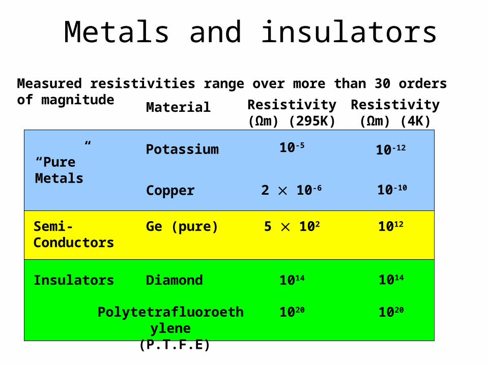
Measured resistivities range over more than 30 orders of magnitude
Material Resistivity (Ωm) (295K)
Resistivity (Ωm) (4K)
10-12
“Pure”Metals
Copper
10-5
Semi-Conductors
Ge (pure) 5 102 1012
Insulators Diamond 1014
Polytetrafluoroethylene (P.T.F.E)
1020
1014
1020
Potassium
2 10-6 10-10
Metals and insulators
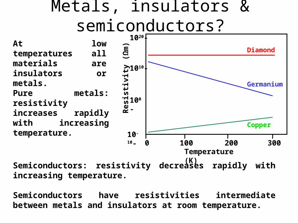
Metals, insulators & semiconductors?
At low temperatures all materials are insulators or metals.
Semiconductors: resistivity decreases rapidly with increasing temperature. Semiconductors have resistivities intermediate between metals and insulators at room temperature.
Pure metals: resistivity increases rapidly with increasing temperature.
1020-
1010-
100 -
10-10-R
esis
tivi
ty (
Ωm
)
100 200 3000Temperature (K)
Diamond
Germanium
Copper
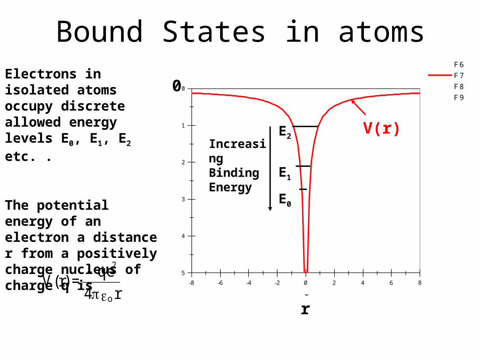
Bound States in atoms
r4
qe = )r(V
o
2
Electrons in isolated atoms occupy discrete allowed energy levels E0, E1, E2 etc. .
The potential energy of an electron a distance r from a positively charge nucleus of charge q is
-8 -6 -4 -2 0 2 4 6 8-5
-4
-3
-2
-1
0
F6 F7 F8 F9
r
V(r)E2
E1
E0
r
0
Increasing Binding Energy
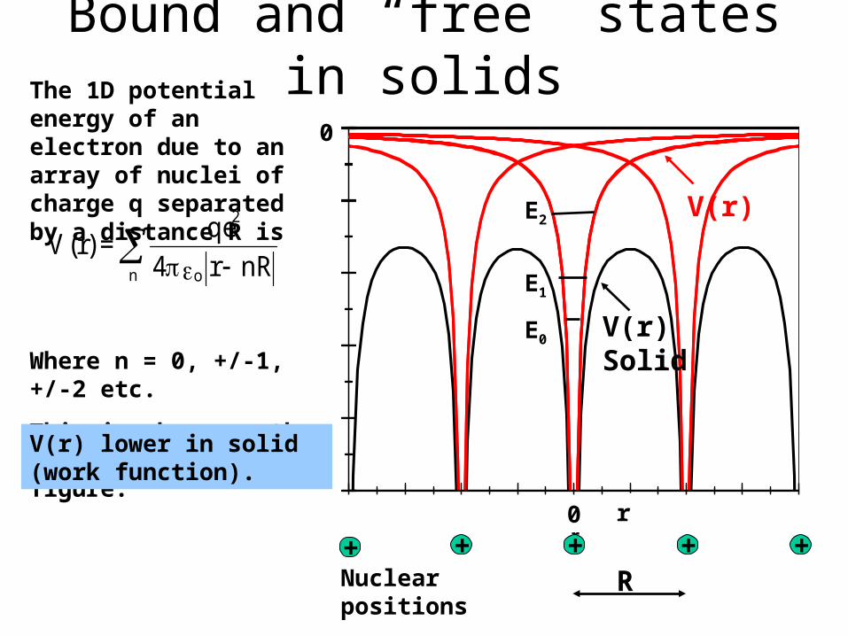
Bound and “free” states in solids
-8 -6 -4 -2 0 2 4 6 8-5
-4
-3
-2
-1
0
F6 F7 F8 F9
r
-8 -6 -4 -2 0 2 4 6 8-5
-4
-3
-2
-1
0
F6 F7 F8 F9
r
-8 -6 -4 -2 0 2 4 6 8-5
-4
-3
-2
-1
0
F6 F7 F8 F9
r
V(r)E2
E1
E0
The 1D potential energy of an electron due to an array of nuclei of charge q separated by a distance R is
Where n = 0, +/-1, +/-2 etc.
This is shown as the black line in the figure.
n o
2
nRr4
qe = )r(V
r
0
0
+ + + + +RNuclear positions
V(r) lower in solid (work function).
V(r)Solid
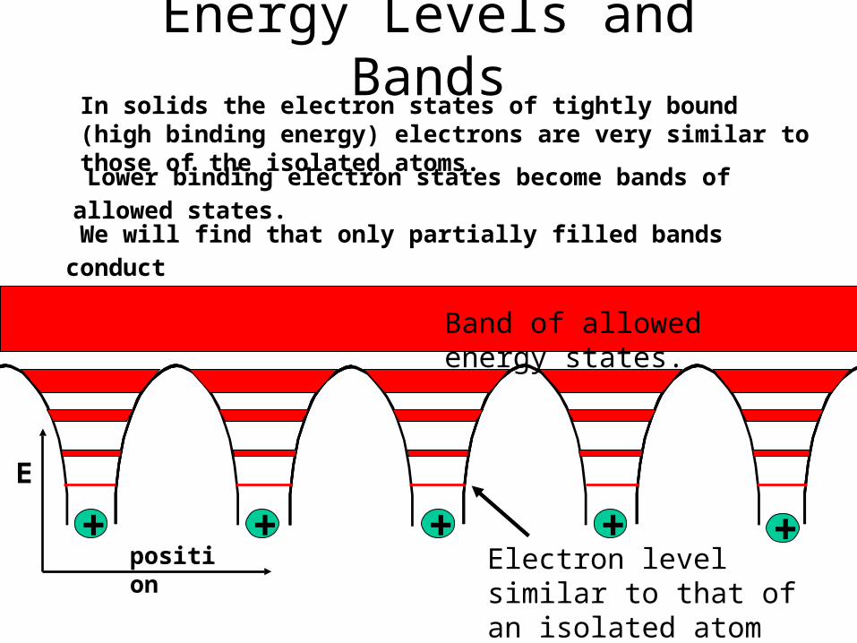
Energy Levels and Bands
+E
+ + + +position Electron level similar to
that of an isolated atom
Band of allowed energy states.
In solids the electron states of tightly bound (high binding energy) electrons are very similar to those of the isolated atoms.
Lower binding electron states become bands of allowed states.
We will find that only partially filled bands conduct
Band TheoryThe calculation of the allowed electron states in a solid is referred to as band theory or band structure theory.
Free electron model
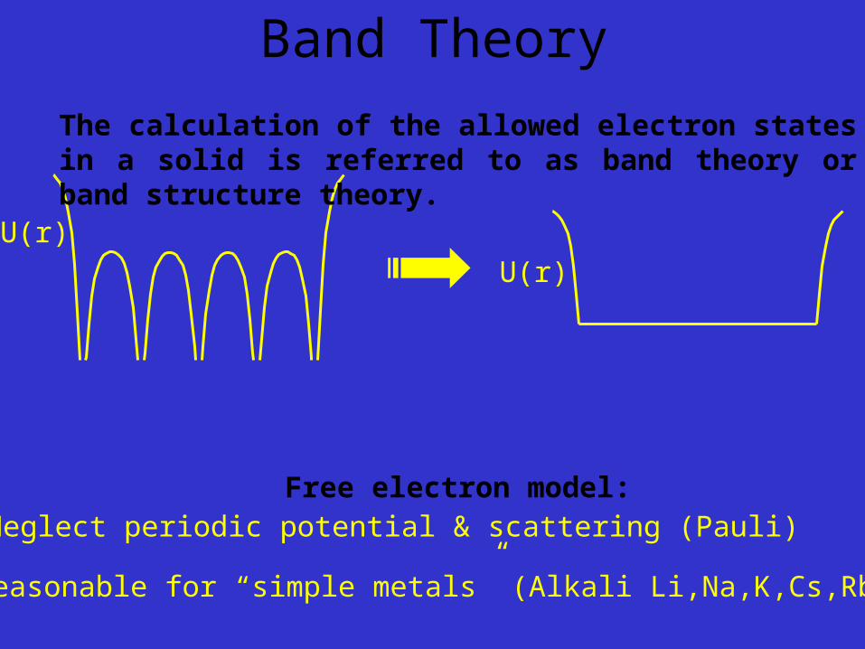
U(r)U(r)
Neglect periodic potential & scattering (Pauli)
Reasonable for “simple metals” (Alkali Li,Na,K,Cs,Rb)
Band Theory
The calculation of the allowed electron states in a solid is referred to as band theory or band structure theory.
Free electron model:
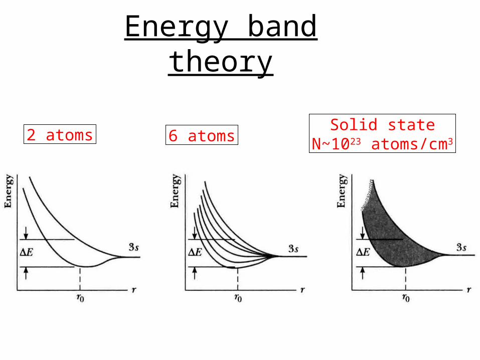
Solid stateN~1023 atoms/cm32 atoms 6 atoms
Energy band theory
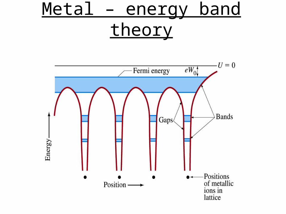
Metal – energy band theory
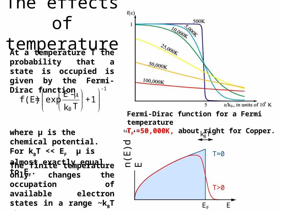
At a temperature T the probability that a state is occupied is given by the Fermi-Dirac function
1 +
Tk
-Eexp = f(E)
B
-1
EEF
N(E
) dE
kBT
T=0
T>0
n(E
)dE
The finite temperature only changes the occupation of available electron states in a range ~kBT about EF.
where μ is the chemical potential. For kBT << EF μ is
almost exactly equal to EF.
Fermi-Dirac function for a Fermi temperature TF =50,000K, about right for Copper.
The effects of temperature
Band theory ctd.
To obtain the full band structure, we need to solve Schrödinger’s equation for the full lattice potential. This cannot be done exactly and various approximation schemes are used. We will introduce two very different models, the nearly free electron and tight binding models.
We will continue to treat the electrons as independent, i.e. neglect the electron-electron interaction.
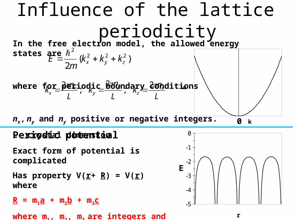
Influence of the lattice periodicityIn the free electron model, the allowed energy states are
where for periodic boundary conditions
nx , ny and ny positive or negative integers.
L- crystal dimension
)(2
2222
zyx kkkm
E
L
nk
L
nk
L
nk z
zy
yx
x
2;
2;
2 E
k0
-5
-4
-3
-2
-1
0
r
E
Periodic potential
Exact form of potential is complicated
Has property V(r+ R) = V(r) where
R = m1a + m2b + m3c
where m1, m2, m3 are integers and a ,b ,c are the primitive lattice vectors.
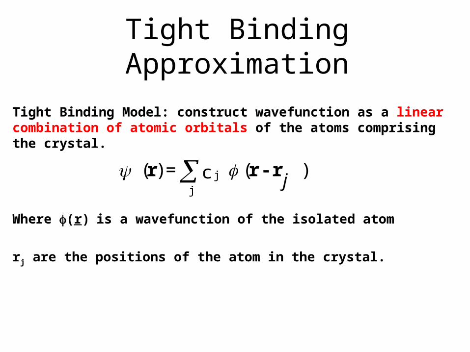
Tight Binding Approximation
Tight Binding Model: construct wavefunction as a linear combination of atomic orbitals of the atoms comprising the crystal.
Where (r)is a wavefunction of the isolated atom
rj are the positions of the atom in the crystal.
) ( c = )( j
jj
r-r r
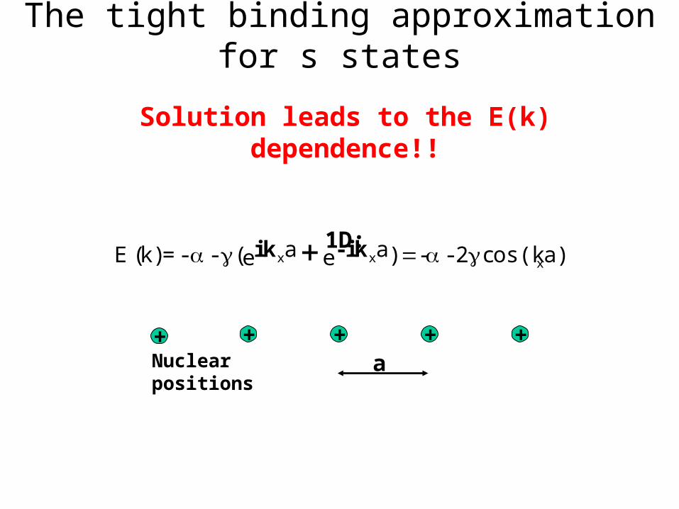
The tight binding approximation for s states
)aos(kc 2- -)e ae a( - - = k)( E xxx k i-k i
+ + + + +aNuclear positions
Solution leads to the E(k) dependence!!
1D:
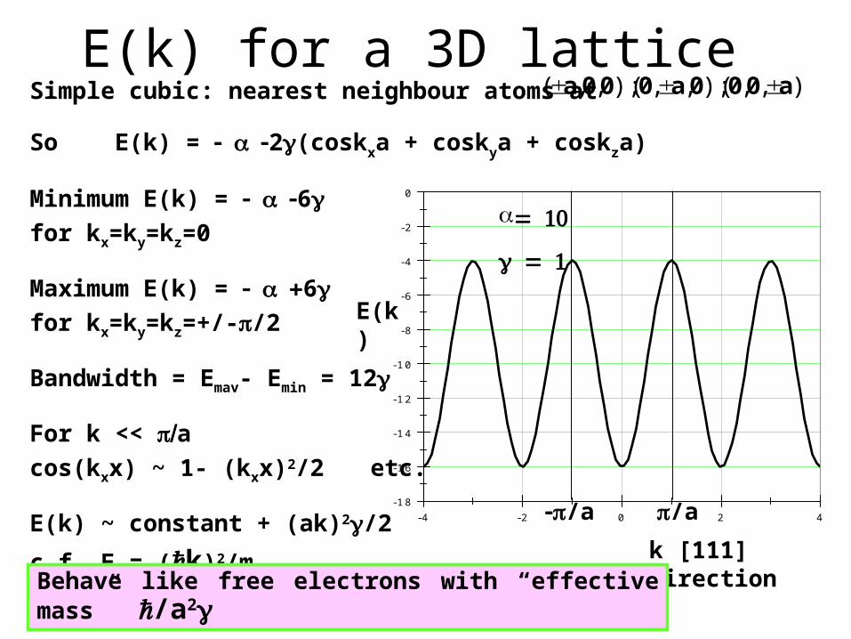
E(k) for a 3D lattice Simple cubic: nearest neighbour atoms at
So E(k) = 2(coskxa + coskya + coskza)
Minimum E(k) = 6for kx=ky=kz=0
Maximum E(k) = 6for kx=ky=kz=+/-/2
Bandwidth = Emav- Emin = 12
For k << acos(kxx) ~ 1- (kxx)2/2 etc.
E(k) ~ constant + (ak)2/2
c.f. E = (k)2/me
),,();,,();,,( a000a000a
-4 -2 0 2 4-18
-16
-14
-12
-10
-8
-6
-4
-2
0
F1
k [111] direction
/a/a
E(k)
Behave like free electrons with “effective mass” /a2
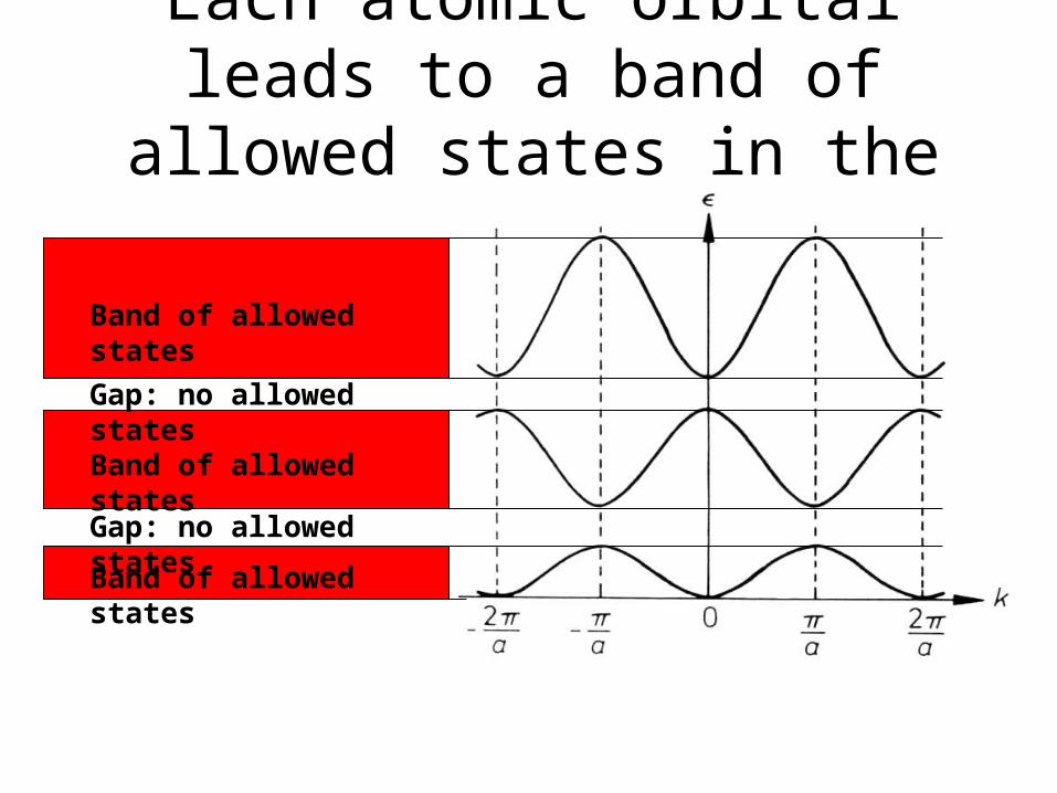
Each atomic orbital leads to a band of allowed states in the solid
Band of allowed states
Band of allowed states
Band of allowed states
Gap: no allowed states
Gap: no allowed states
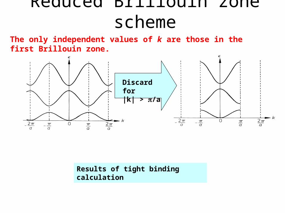
Reduced Brillouin zone scheme
The only independent values of k are those in the first Brillouin zone.
Results of tight binding calculation
Discard for |k| > /a
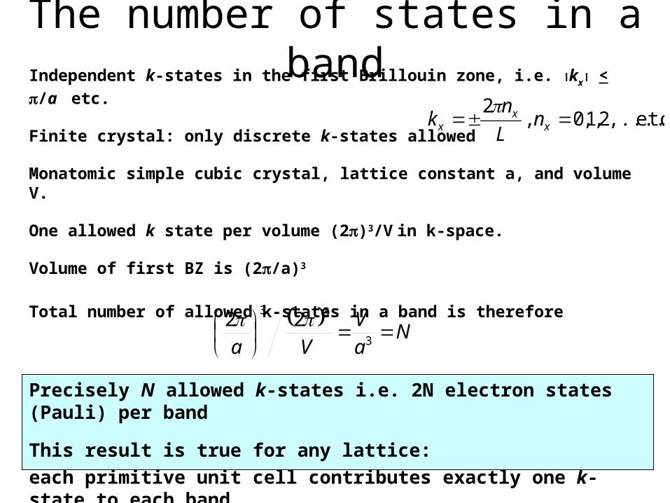
The number of states in a bandIndependent k-states in the first Brillouin zone, i.e. kx < /a etc.
Finite crystal: only discrete k-states allowed
Monatomic simple cubic crystal, lattice constant a, and volume V.
One allowed k state per volume (2)3/V in k-space.
Volume of first BZ is (2/a)3
Total number of allowed k-states in a band is therefore
.etc,....2,1,0,2
xx
x nL
nk
N
aV
Va
3
3322
Precisely N allowed k-states i.e. 2N electron states (Pauli) per band
This result is true for any lattice:
each primitive unit cell contributes exactly one k-state to each band.
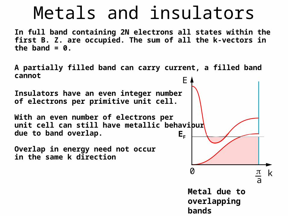
Metals and insulatorsIn full band containing 2N electrons all states within the first B. Z. are occupied. The sum of all the k-vectors in the band = 0.
A partially filled band can carry current, a filled band cannot
Insulators have an even integer numberof electrons per primitive unit cell.
With an even number of electrons perunit cell can still have metallic behaviourdue to band overlap.
Overlap in energy need not occurin the same k direction
E
k0 a
EF
Metal due to overlapping bands
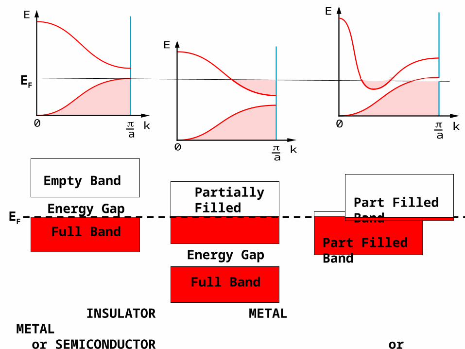
Full Band
Empty Band
Energy Gap
Full Band
Partially Filled Band
Energy GapPart Filled Band
Part Filled Band EF
INSULATOR METAL METAL or SEMICONDUCTOR or SEMI-METAL
E
k0 a
EF
E
k0 a
E
k0 a
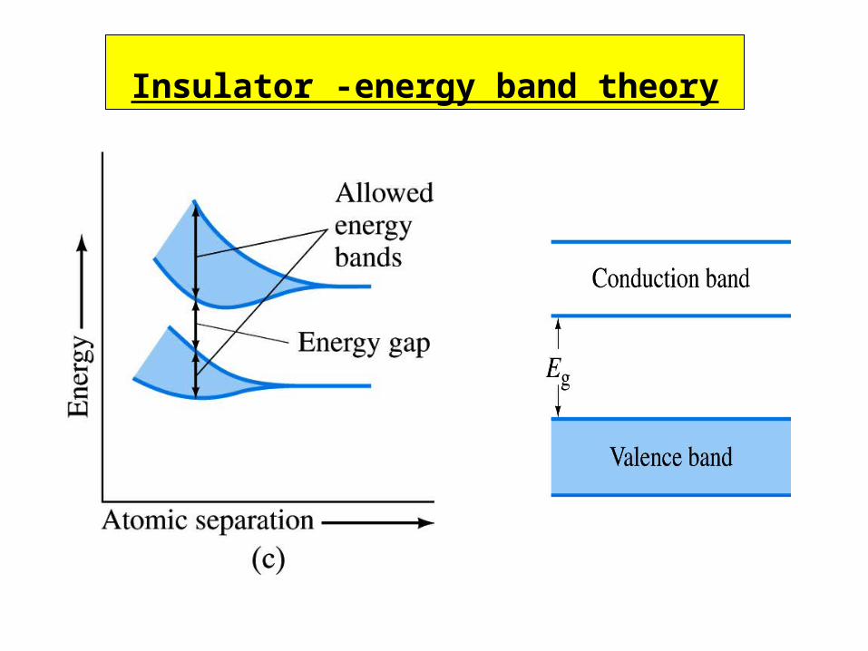
Insulator -energy band theory
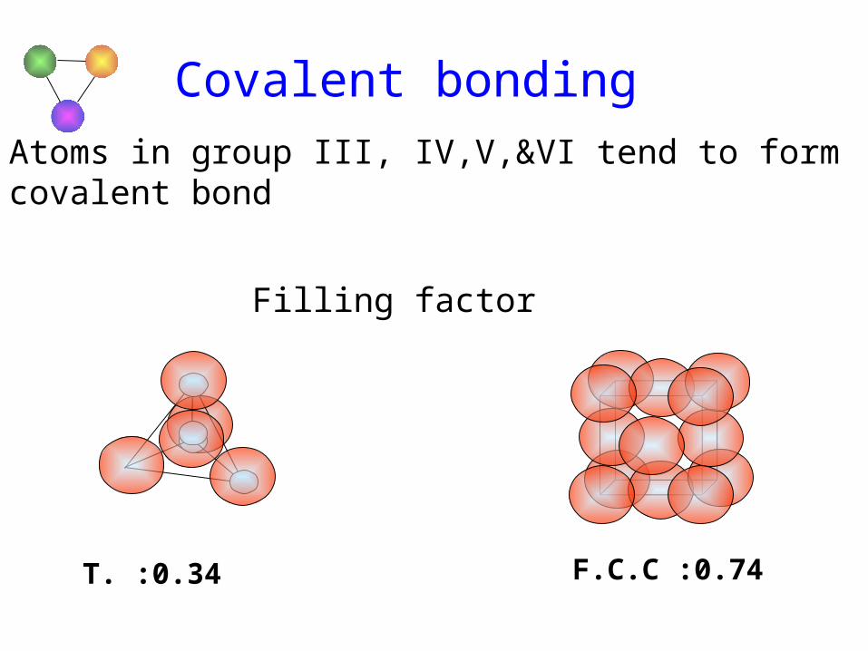
Covalent bonding
Atoms in group III, IV,V,&VI tend to form covalent bond
Filling factor
T. :0.34 F.C.C :0.74
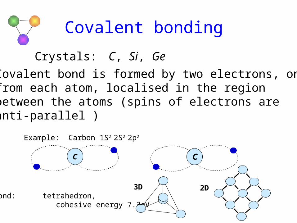
Covalent bonding
Crystals: C, Si, Ge
Covalent bond is formed by two electrons, one from each atom, localised in the region between the atoms (spins of electrons areanti-parallel )
Example: Carbon 1S2 2S2 2p2
C C
Diamond: tetrahedron, cohesive energy 7.3eV
3D 2D
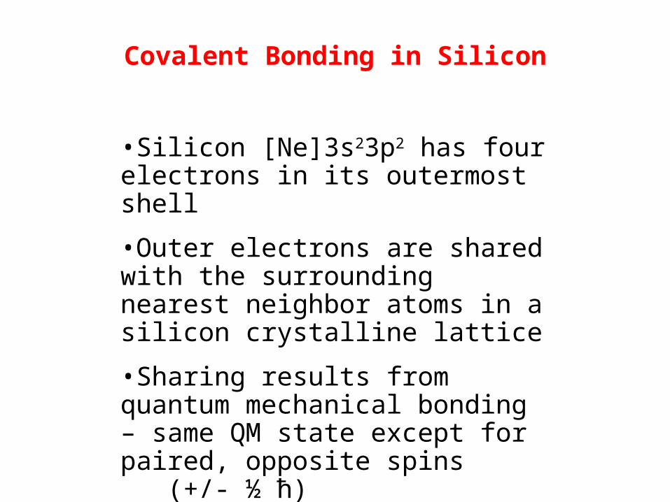
Covalent Bonding in Silicon
•Silicon [Ne]3s23p2 has four electrons in its outermost shell
•Outer electrons are shared with the surrounding nearest neighbor atoms in a silicon crystalline lattice
•Sharing results from quantum mechanical bonding – same QM state except for paired, opposite spins (+/- ½ ħ)
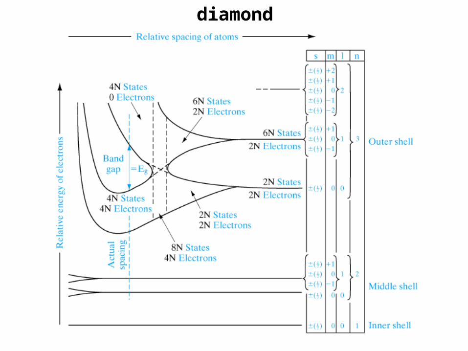
diamond
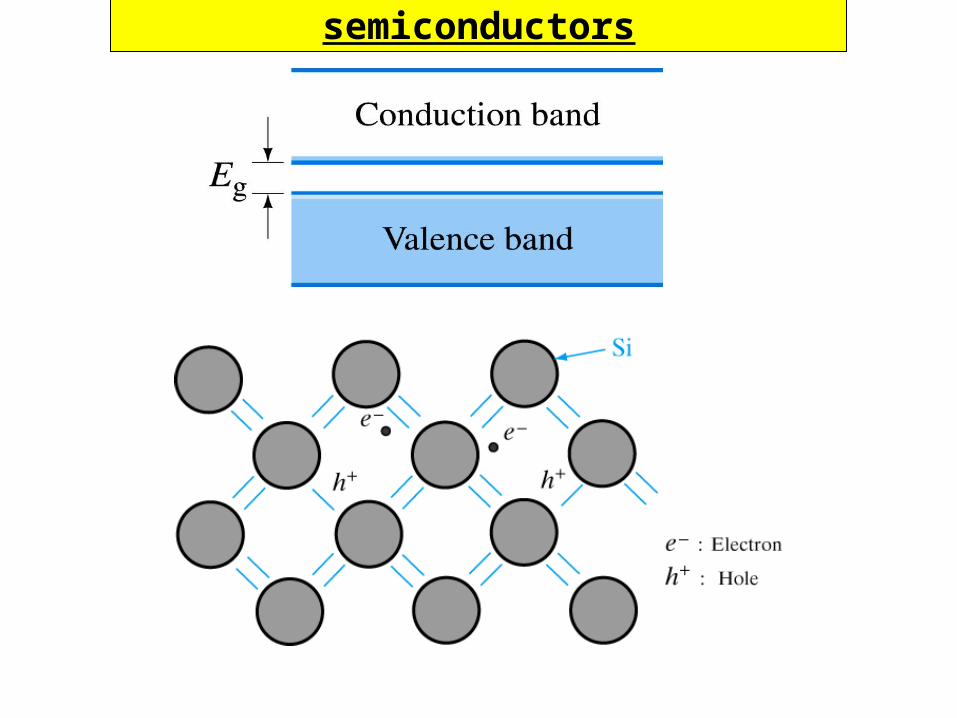
semiconductors
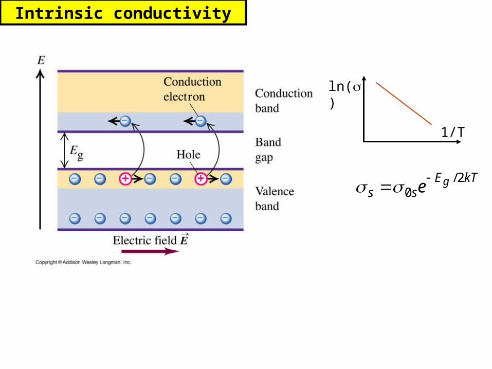
Intrinsic conductivity
kTEss
ge2/
0
ln()
1/T
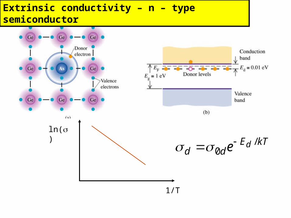
1/T
ln()
kTEdd
de /0
Extrinsic conductivity – n – type semiconductor
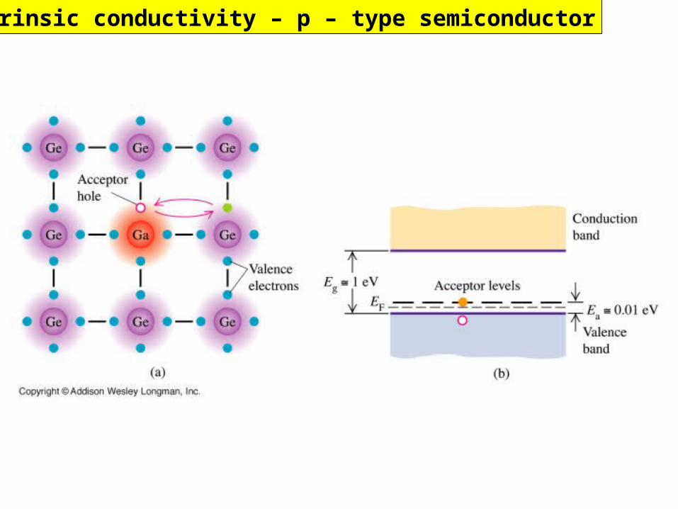
Extrinsic conductivity – p – type semiconductor
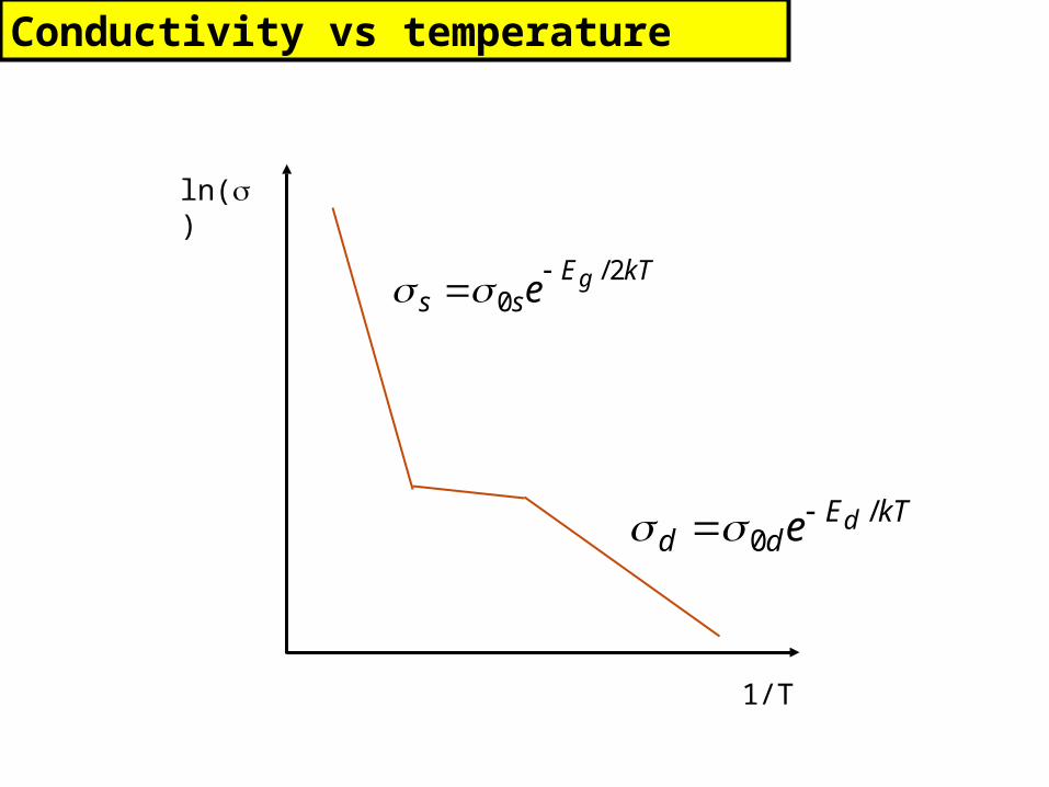
Conductivity vs temperature
kTEss
ge2/
0
ln()
kTEdd
de /0
1/T
ActiniumAluminium (Aluminum)AmericiumAntimonyArgonArsenicAstatineBariumBerkeliumBerylliumBismuthBohriumBoronBromineCadmiumCaesium (Cesium)CalciumCaliforniumCarbonCerium
ChlorineChromiumCobaltCopperCuriumDarmstadtiumDubniumDysprosiumEinsteiniumErbiumEuropiumFermiumFluorineFranciumGadoliniumGalliumGermaniumGoldHafniumHassium
HeliumHolmiumHydrogenIndiumIodineIridiumIronKryptonLanthanumLawrenciumLeadLithiumLutetiumMagnesiumManganeseMeitneriumMendeleviumMercuryMolybdenumNeodymium
NeonNeptuniumNickelNiobiumNitrogenNobeliumOsmiumOxygenPalladiumPhosphorusPlatinumPlutoniumPoloniumPotassiumPraseodymiumPromethiumProtactiniumRadiumRadonRhenium
RhodiumRubidiumRutheniumRutherfordiumSamariumScandiumSeaborgiumSeleniumSiliconSilverSodiumStrontiumSulfur (Sulphur)TantalumTechnetiumTelluriumTerbiumThalliumThoriumThulium
TinTitaniumTungstenUnunbiumUnunhexiumUnunoctiumUnunpentiumUnunquadiumUnunseptiumUnuntriumUraniumVanadiumXenonYtterbiumYttriumZincZirconium
![RESISTIVITY [ ]](https://static.fdocument.org/doc/165x107/6249524a7a9f6a12787a8128/resistivity-.jpg)


![1) Resistivity of a wire depends on...1) Resistivity of a wire depends on A [ ]) length B [v]) material C [ ]) cross section area D [ ]) none of the above 2) If 1 A current flows in](https://static.fdocument.org/doc/165x107/5e822bdb7755860f623263fd/1-resistivity-of-a-wire-depends-on-1-resistivity-of-a-wire-depends-on-a-.jpg)