woodwardruleStructural Analysis (Application of Woodward-Fieser Rules) of spectroscopy
1
Introduction toCMOS VLSI
Design
Lecture 1A: Manufacturing& Layout
David Harris
Harvey Mudd CollegeSpring 2004
Steven LevitanFall 2008

2
EE1412
© Digital Integrated Circuits2nd Manufacturing
The Manufacturing ProcessThe Manufacturing Process
For a great tour through the IC manufacturing process and its different steps, checkhttp://www.fullman.com/semiconductors/semiconductors.html
3
1: Circuits & Layout Slide 3CMOS VLSI Design
CMOS FabricationCMOS transistors are fabricated on silicon waferLithography process similar to printing pressOn each step, different materials are deposited or etchedEasiest to understand by viewing both top and cross-section of wafer in a simplified manufacturing process
4
EE1414
© Digital Integrated Circuits2nd Manufacturing
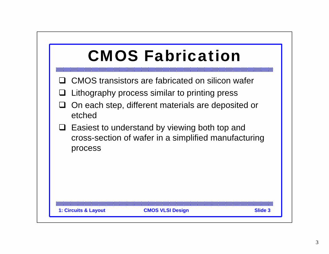
oxidation
opticalmask
processstep
photoresist coatingphotoresistremoval (ashing)
spin, rinse, dryacid etch
photoresist
stepper exposure
development
Typical operations in a single photolithographic cycle (from [Fullman]).
PhotoPhoto--Lithographic ProcessLithographic Process
5
EE1415
© Digital Integrated Circuits2nd Manufacturing
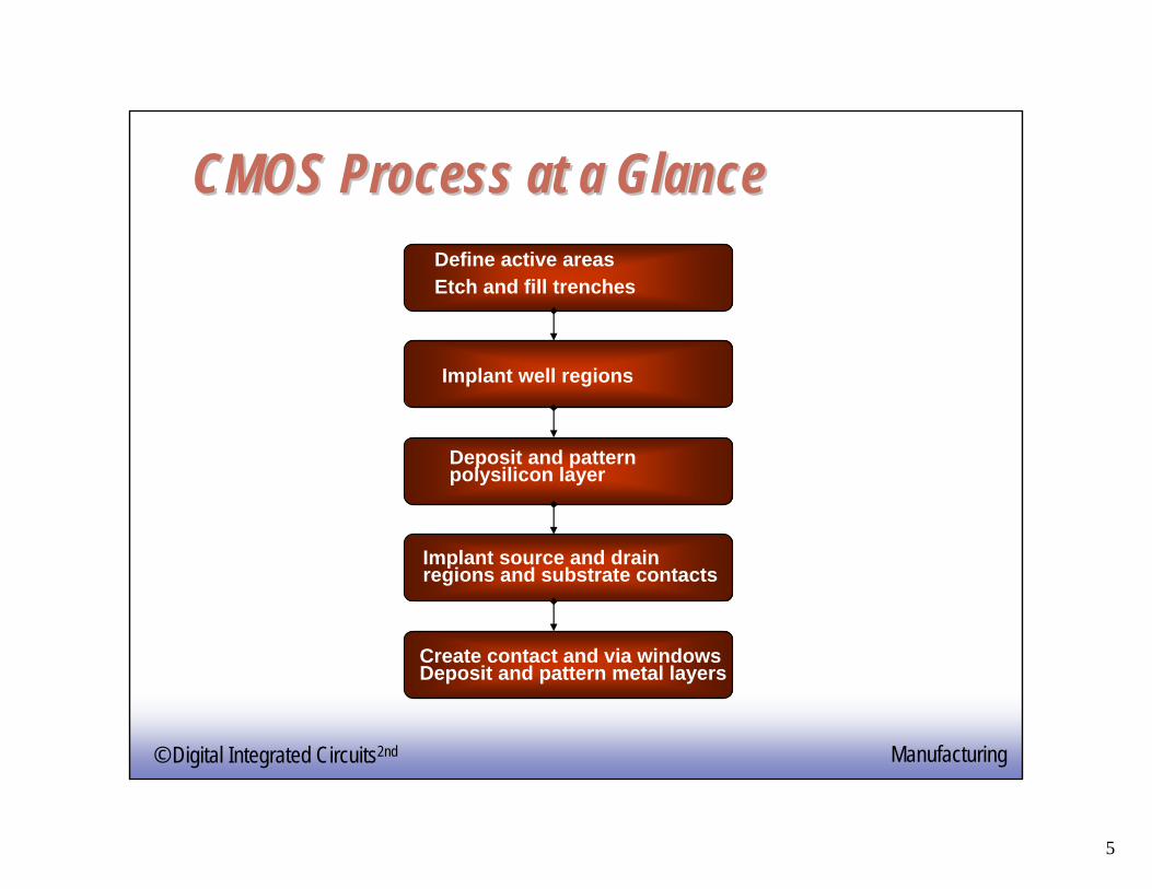
CMOS Process at a GlanceCMOS Process at a GlanceDefine active areasEtch and fill trenches
Implant well regions
Deposit and patternpolysilicon layer
Implant source and drainregions and substrate contacts
Create contact and via windowsDeposit and pattern metal layers
6
EE1416
© Digital Integrated Circuits2nd Manufacturing
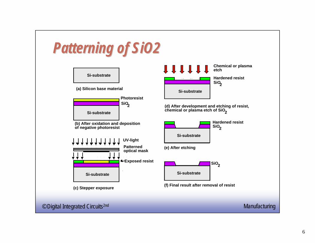
Patterning of SiO2Patterning of SiO2Si-substrate
Si-substrate Si-substrate
(a) Silicon base material
(b) After oxidation and depositionof negative photoresist
(c) Stepper exposure
PhotoresistSiO2
UV-lightPatternedoptical mask
Exposed resist
SiO2
Si-substrate
Si-substrate
Si-substrate
SiO2
SiO2
(d) After development and etching of resist,chemical or plasma etch of SiO2
(e) After etching
(f) Final result after removal of resist
Hardened resist
Hardened resist
Chemical or plasmaetch
7
EE1417
© Digital Integrated Circuits2nd ManufacturingCopyright © 2005 Pearson Addison-Wesley. All rights reserved.
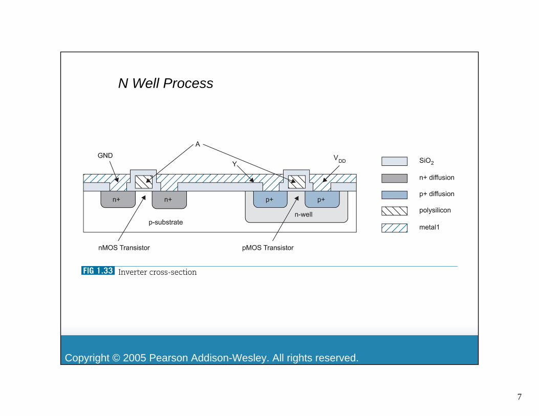
N Well Process
8
1: Circuits & Layout Slide 8CMOS VLSI Design
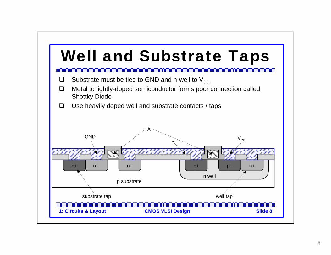
Well and Substrate TapsSubstrate must be tied to GND and n-well to VDD
Metal to lightly-doped semiconductor forms poor connection called Shottky DiodeUse heavily doped well and substrate contacts / taps
n+
p substrate
p+
n well
A
YGND VDD
n+p+
substrate tap well tap
n+ p+
9
1: Circuits & Layout Slide 9CMOS VLSI Design
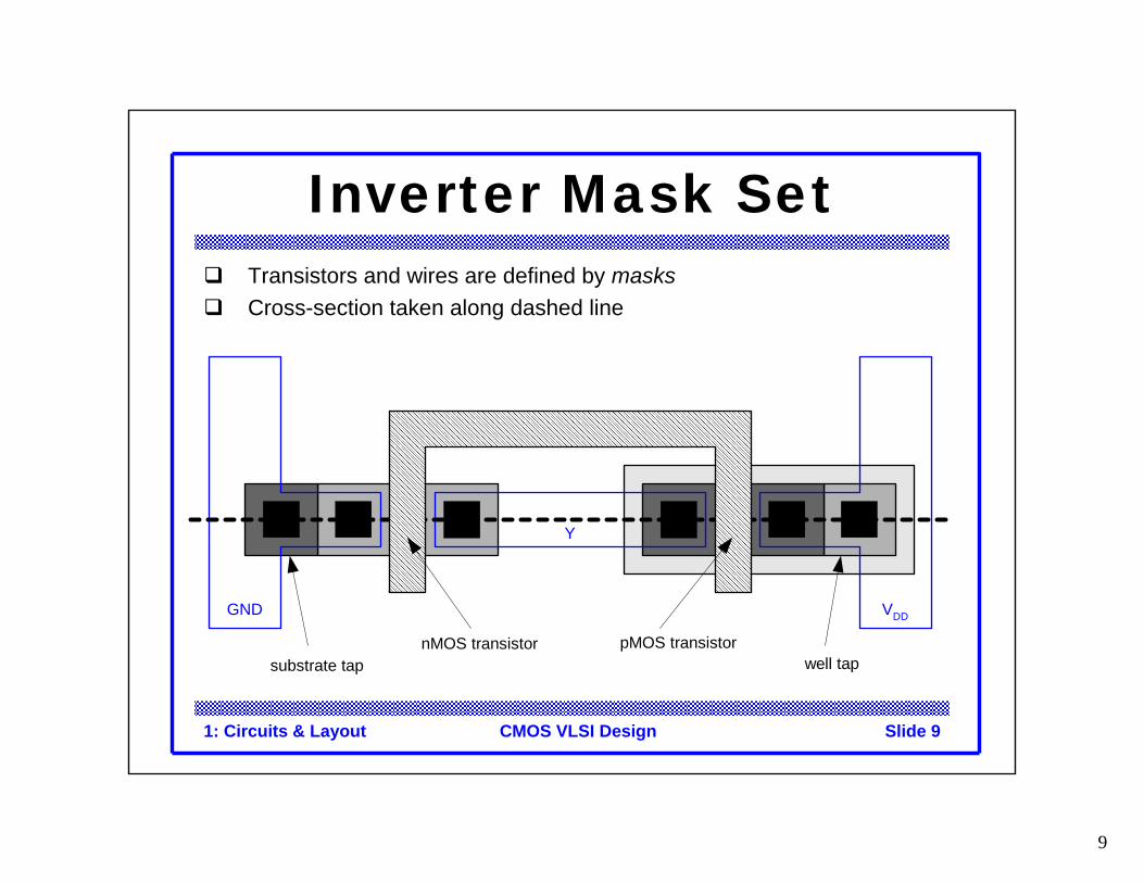
Inverter Mask SetTransistors and wires are defined by masksCross-section taken along dashed line
GND VDD
Y
A
substrate tap well tapnMOS transistor pMOS transistor
10
1: Circuits & Layout Slide 10CMOS VLSI Design
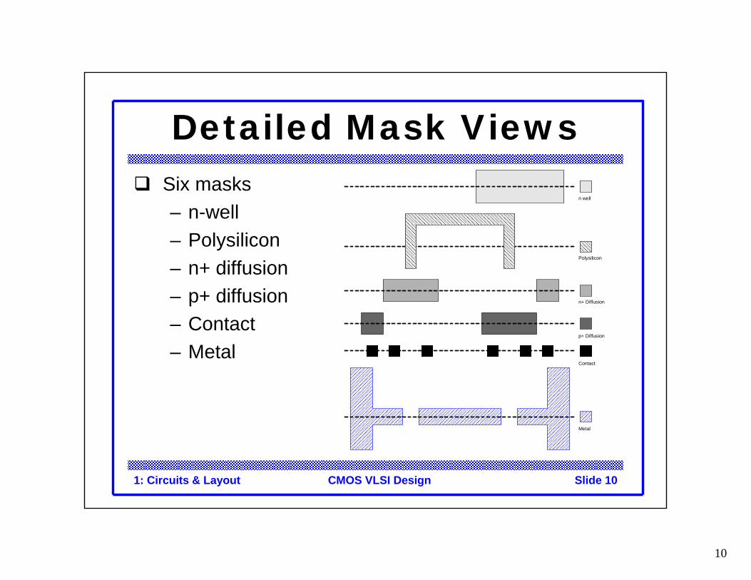
Detailed Mask ViewsSix masks– n-well– Polysilicon– n+ diffusion– p+ diffusion– Contact– Metal
Metal
Polysilicon
Contact
n+ Diffusion
p+ Diffusion
n well
11
EE14111
© Digital Integrated Circuits2nd ManufacturingCopyright © 2005 Pearson Addison-Wesley. All rights reserved.
12
1: Circuits & Layout Slide 12CMOS VLSI Design
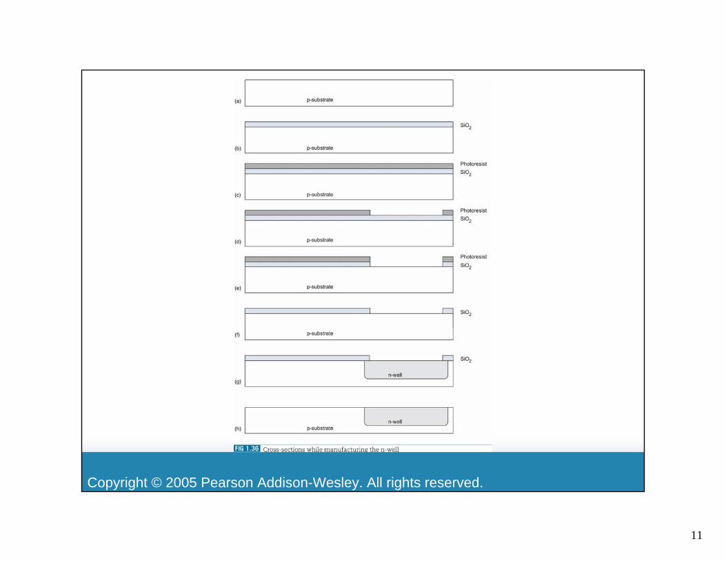
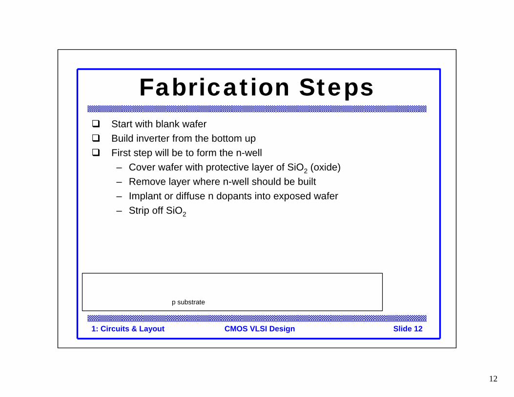
Fabrication StepsStart with blank waferBuild inverter from the bottom upFirst step will be to form the n-well– Cover wafer with protective layer of SiO2 (oxide)– Remove layer where n-well should be built– Implant or diffuse n dopants into exposed wafer– Strip off SiO2
p substrate
13
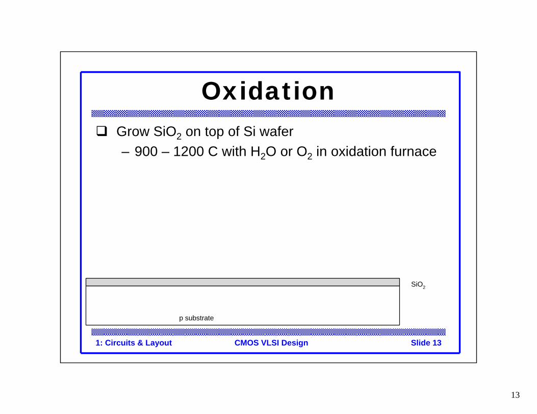
1: Circuits & Layout Slide 13CMOS VLSI Design
OxidationGrow SiO2 on top of Si wafer– 900 – 1200 C with H2O or O2 in oxidation furnace
p substrate
SiO2
14
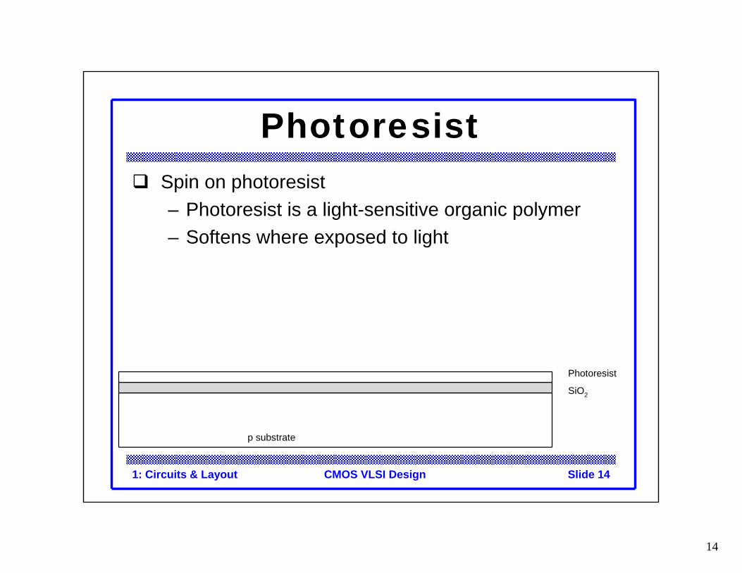
1: Circuits & Layout Slide 14CMOS VLSI Design
PhotoresistSpin on photoresist– Photoresist is a light-sensitive organic polymer– Softens where exposed to light
p substrate
SiO2
Photoresist
15
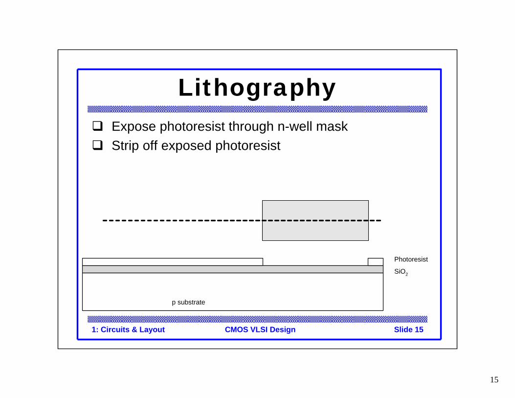
1: Circuits & Layout Slide 15CMOS VLSI Design
LithographyExpose photoresist through n-well maskStrip off exposed photoresist
p substrate
SiO2
Photoresist
16
1: Circuits & Layout Slide 16CMOS VLSI Design
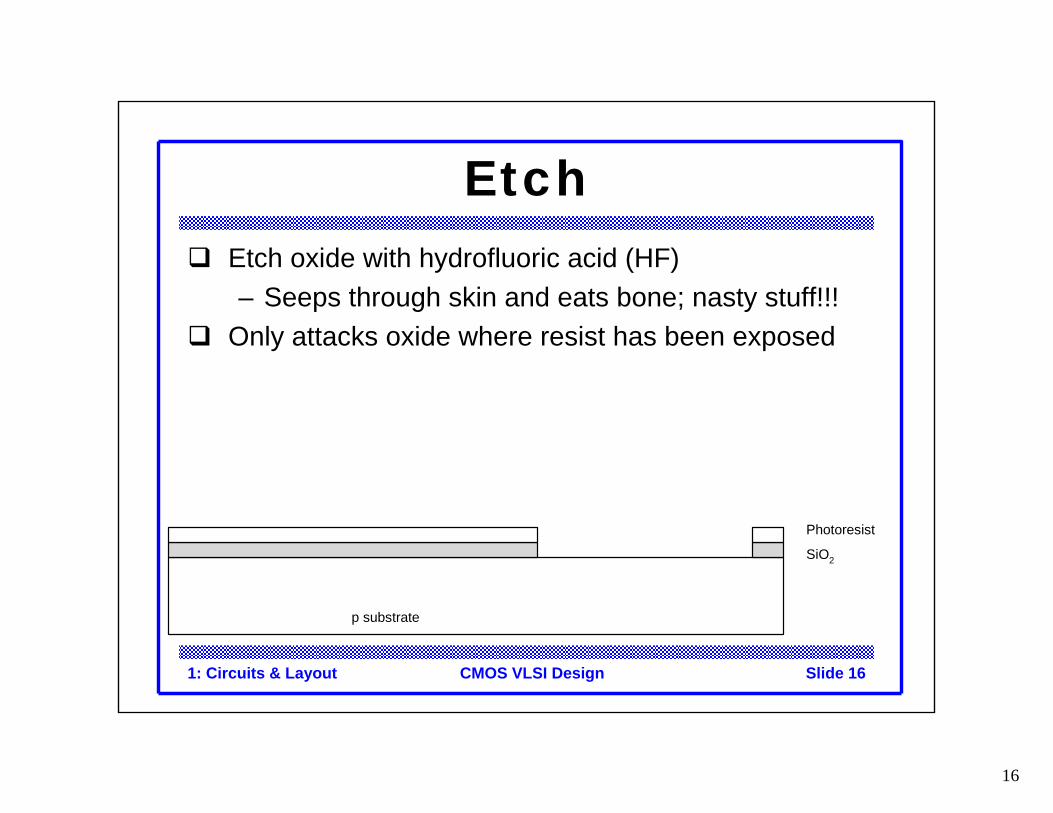
EtchEtch oxide with hydrofluoric acid (HF)– Seeps through skin and eats bone; nasty stuff!!!
Only attacks oxide where resist has been exposed
p substrate
SiO2
Photoresist
17
1: Circuits & Layout Slide 17CMOS VLSI Design
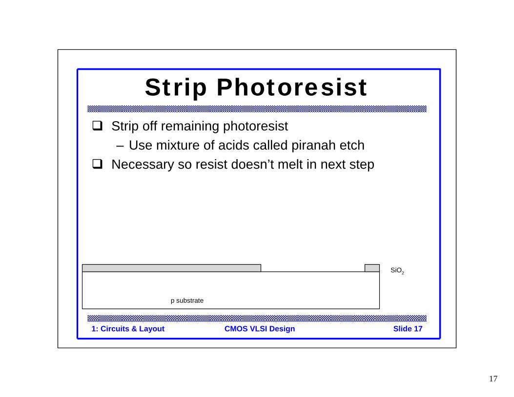
Strip PhotoresistStrip off remaining photoresist– Use mixture of acids called piranah etch
Necessary so resist doesn’t melt in next step
p substrate
SiO2
18
1: Circuits & Layout Slide 18CMOS VLSI Design
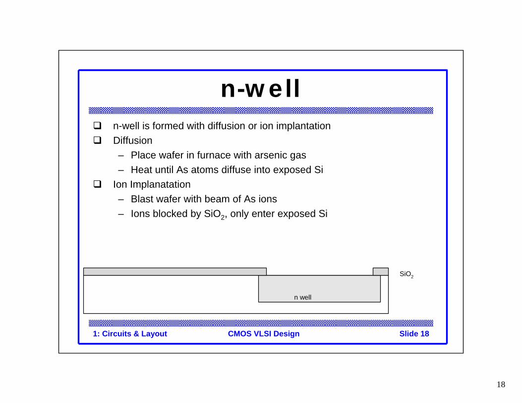
n-welln-well is formed with diffusion or ion implantationDiffusion– Place wafer in furnace with arsenic gas– Heat until As atoms diffuse into exposed Si
Ion Implanatation– Blast wafer with beam of As ions– Ions blocked by SiO2, only enter exposed Si
n well
SiO2
19
1: Circuits & Layout Slide 19CMOS VLSI Design
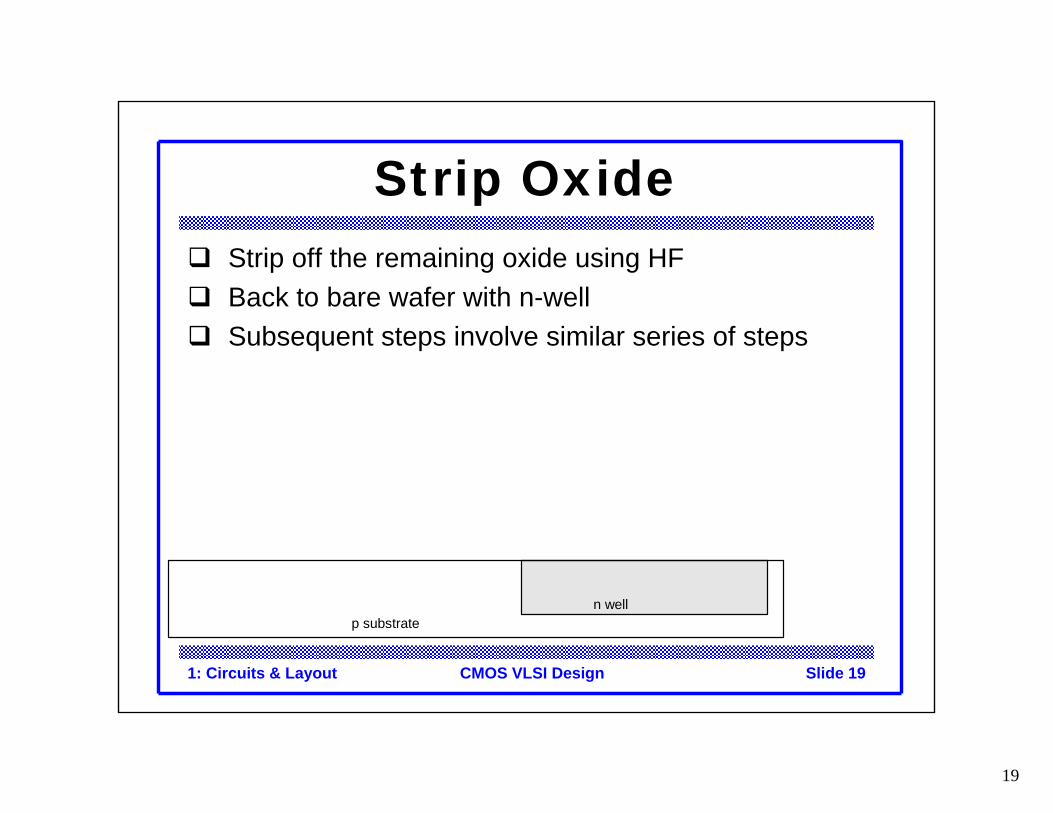
Strip OxideStrip off the remaining oxide using HFBack to bare wafer with n-wellSubsequent steps involve similar series of steps
p substraten well
20
EE14120
© Digital Integrated Circuits2nd ManufacturingCopyright © 2005 Pearson Addison-Wesley. All rights reserved.
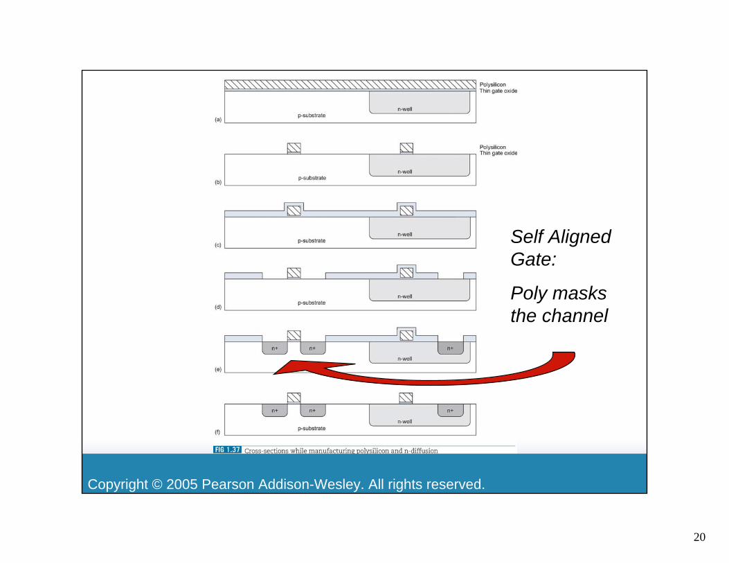
Self Aligned Gate:
Poly masks the channel
21
1: Circuits & Layout Slide 21CMOS VLSI Design
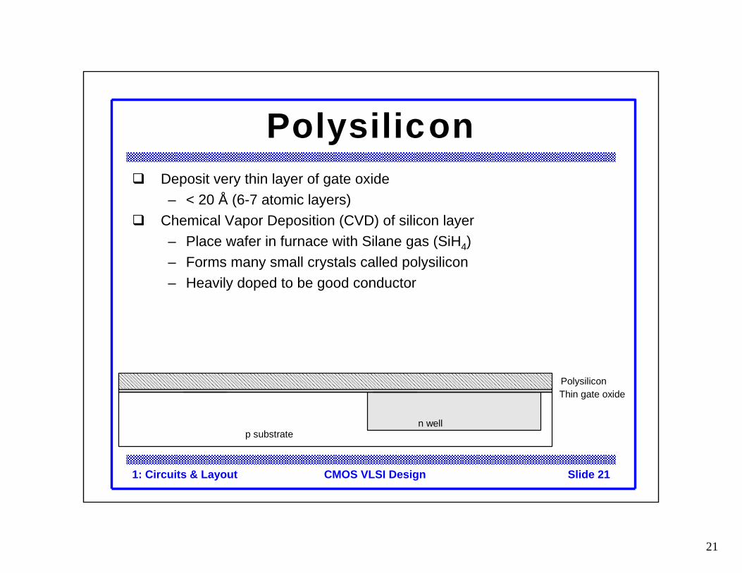
PolysiliconDeposit very thin layer of gate oxide– < 20 Å (6-7 atomic layers)
Chemical Vapor Deposition (CVD) of silicon layer– Place wafer in furnace with Silane gas (SiH4)– Forms many small crystals called polysilicon– Heavily doped to be good conductor
Thin gate oxidePolysilicon
p substraten well
22
1: Circuits & Layout Slide 22CMOS VLSI Design
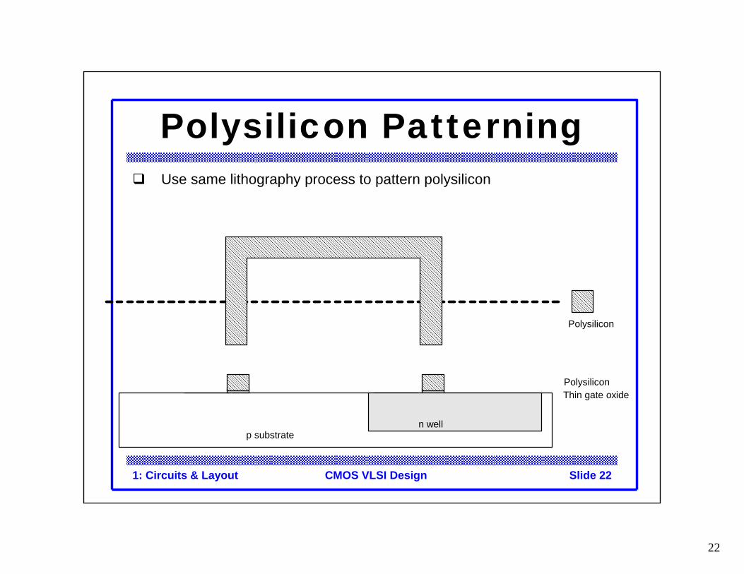
Polysilicon PatterningUse same lithography process to pattern polysilicon
Polysilicon
p substrate
Thin gate oxidePolysilicon
n well
23
1: Circuits & Layout Slide 23CMOS VLSI Design
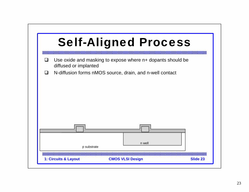
Self-Aligned ProcessUse oxide and masking to expose where n+ dopants should be diffused or implantedN-diffusion forms nMOS source, drain, and n-well contact
p substraten well
24
1: Circuits & Layout Slide 24CMOS VLSI Design
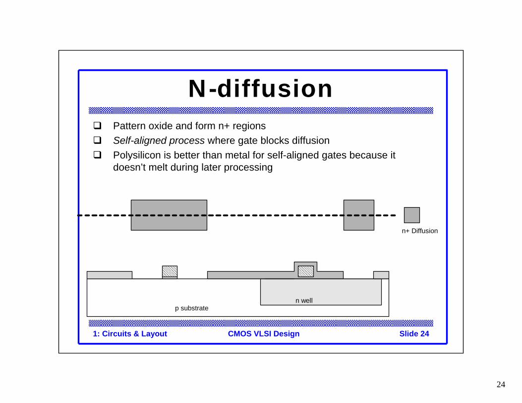
N-diffusionPattern oxide and form n+ regionsSelf-aligned process where gate blocks diffusionPolysilicon is better than metal for self-aligned gates because it doesn’t melt during later processing
p substraten well
n+ Diffusion
25
1: Circuits & Layout Slide 25CMOS VLSI Design
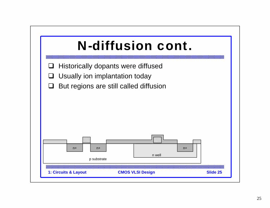
N-diffusion cont.Historically dopants were diffusedUsually ion implantation todayBut regions are still called diffusion
n wellp substrate
n+n+ n+
26
1: Circuits & Layout Slide 26CMOS VLSI Design
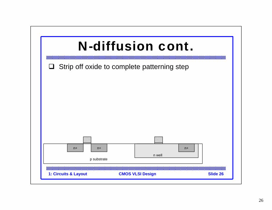
N-diffusion cont.Strip off oxide to complete patterning step
n wellp substrate
n+n+ n+
27
EE14127
© Digital Integrated Circuits2nd ManufacturingCopyright © 2005 Pearson Addison-Wesley. All rights reserved.
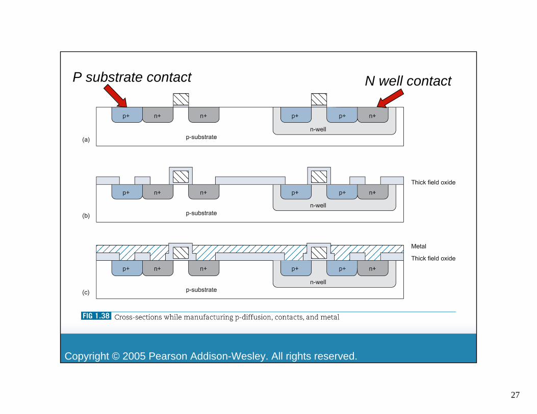
N well contactP substrate contact
28
1: Circuits & Layout Slide 28CMOS VLSI Design
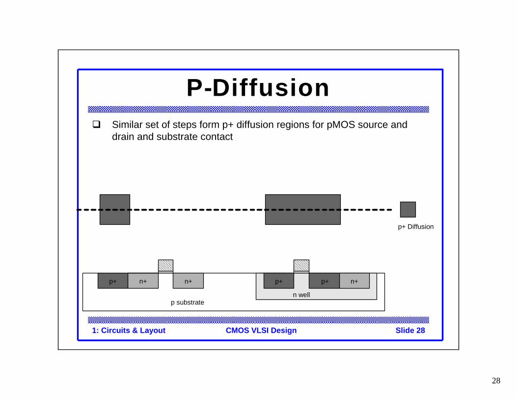
P-DiffusionSimilar set of steps form p+ diffusion regions for pMOS source and drain and substrate contact
p+ Diffusion
p substraten well
n+n+ n+p+p+p+
29
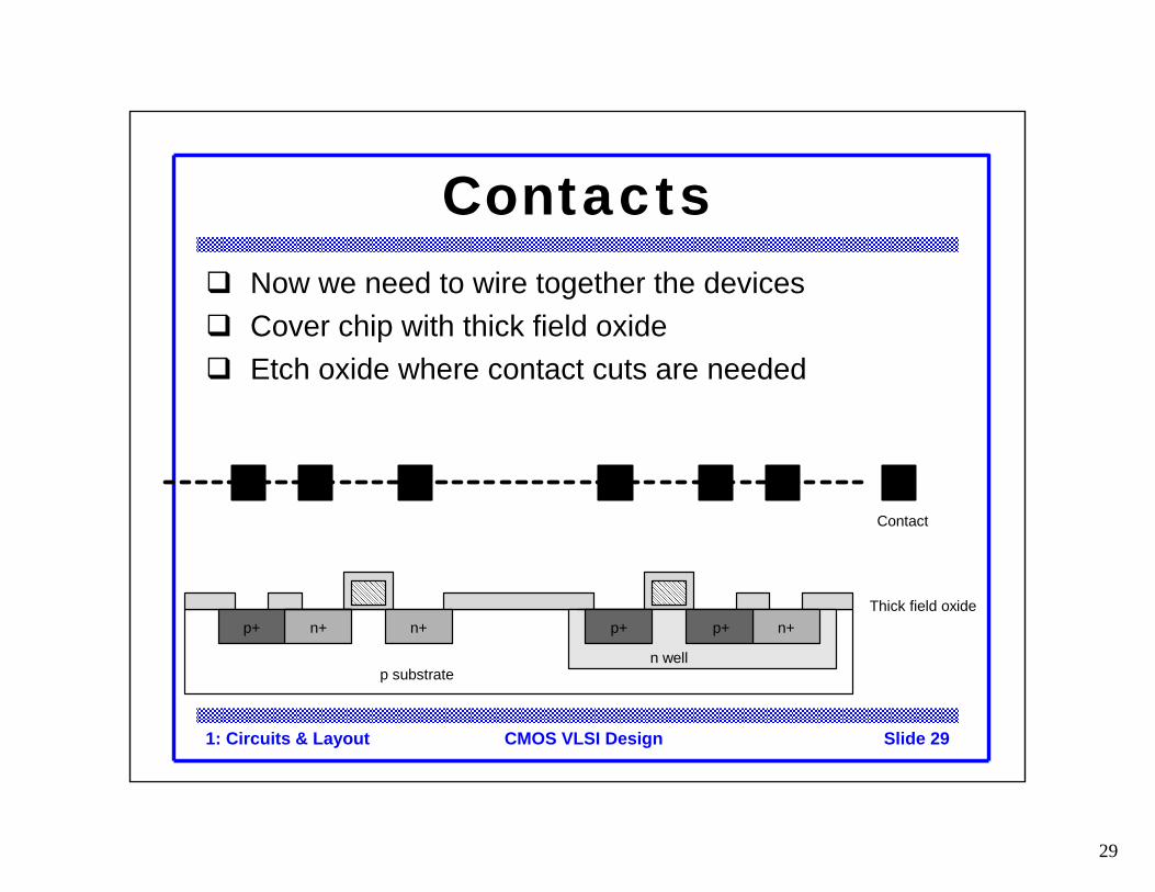
1: Circuits & Layout Slide 29CMOS VLSI Design
ContactsNow we need to wire together the devicesCover chip with thick field oxideEtch oxide where contact cuts are needed
p substrate
Thick field oxide
n well
n+n+ n+p+p+p+
Contact
30
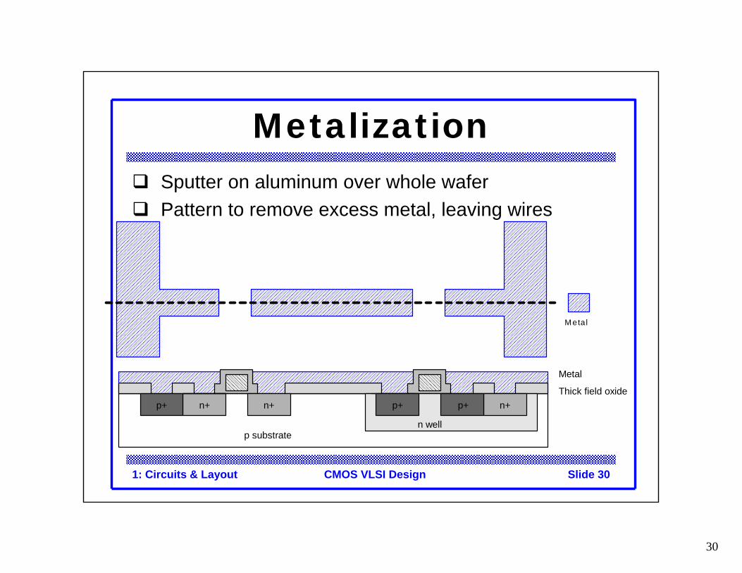
1: Circuits & Layout Slide 30CMOS VLSI Design
MetalizationSputter on aluminum over whole waferPattern to remove excess metal, leaving wires
p substrate
Metal
Thick field oxide
n well
n+n+ n+p+p+p+
M etal
31
EE14131
© Digital Integrated Circuits2nd Manufacturing
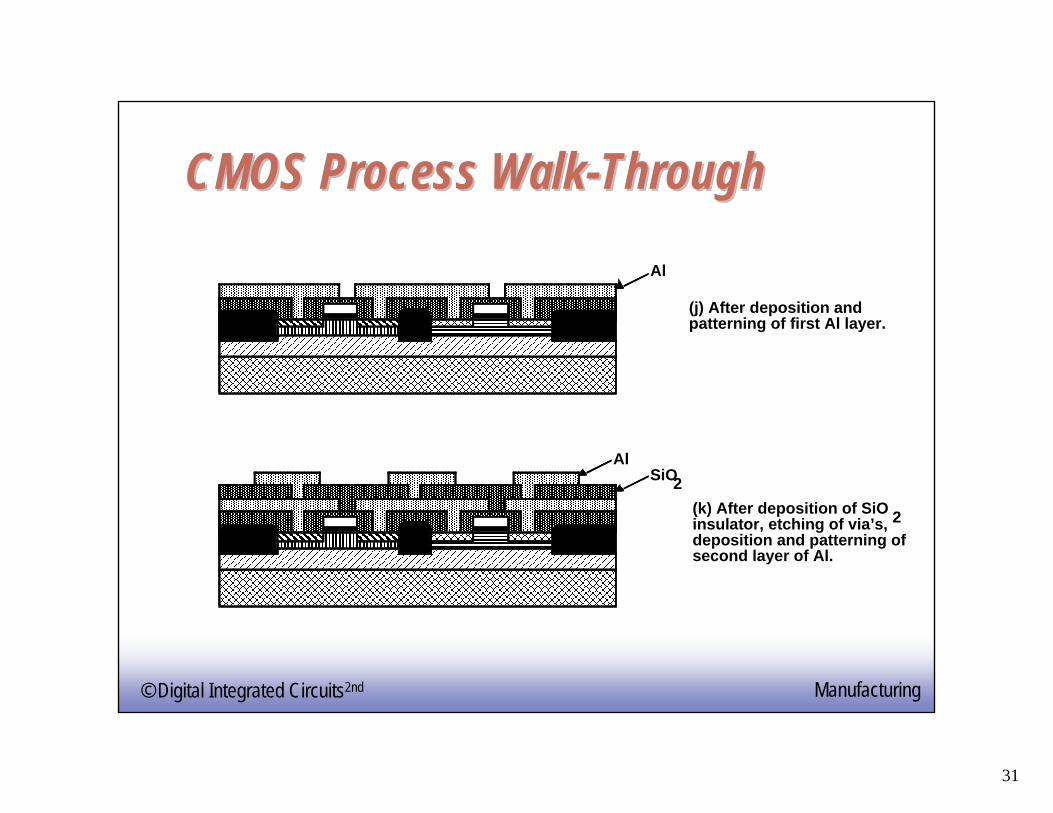
CMOS Process WalkCMOS Process Walk--ThroughThrough
(j) After deposition and patterning of first Al layer.
Al
(k) After deposition of SiO 2insulator, etching of via’s,deposition and patterning ofsecond layer of Al.
AlSiO2
32
EE14132
© Digital Integrated Circuits2nd Manufacturing
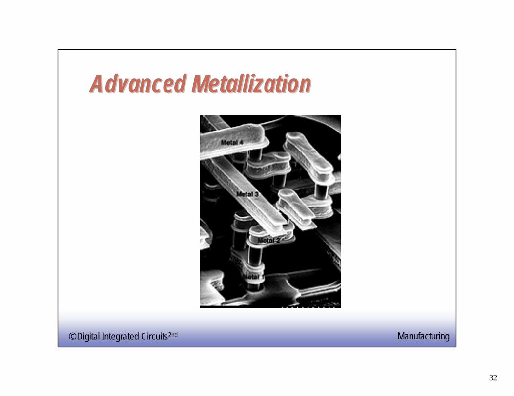
Advanced MetallizationAdvanced Metallization
33
EE14133
© Digital Integrated Circuits2nd Manufacturing
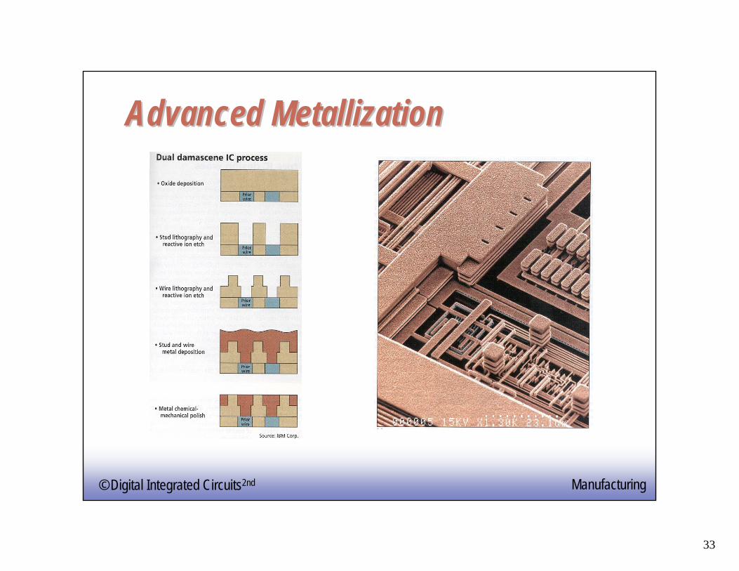
Advanced MetallizationAdvanced Metallization
34
1: Circuits & Layout Slide 34CMOS VLSI Design
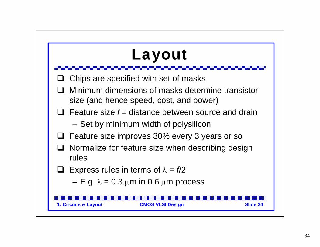
LayoutChips are specified with set of masksMinimum dimensions of masks determine transistor size (and hence speed, cost, and power)Feature size f = distance between source and drain– Set by minimum width of polysilicon
Feature size improves 30% every 3 years or soNormalize for feature size when describing design rulesExpress rules in terms of λ = f/2– E.g. λ = 0.3 μm in 0.6 μm process
35
EE14135
© Digital Integrated Circuits2nd Manufacturing
Design RulesDesign RulesInterface between designer and process engineerGuidelines for constructing process masksUnit dimension: Minimum line width
scalable design rules: lambda parameterabsolute dimensions (micron rules)
Rules fromManufacturing process (antenna rules)Final result (shorts/opens)
Could beElectrical – maximum currentMechanical – surface planarityThermal - overheatingOptical – mask requirementsCharacterization – only some size transistors well characterized
Rules used to be 3 pages, now a book, soon worse…
36
1: Circuits & Layout Slide 36CMOS VLSI Design
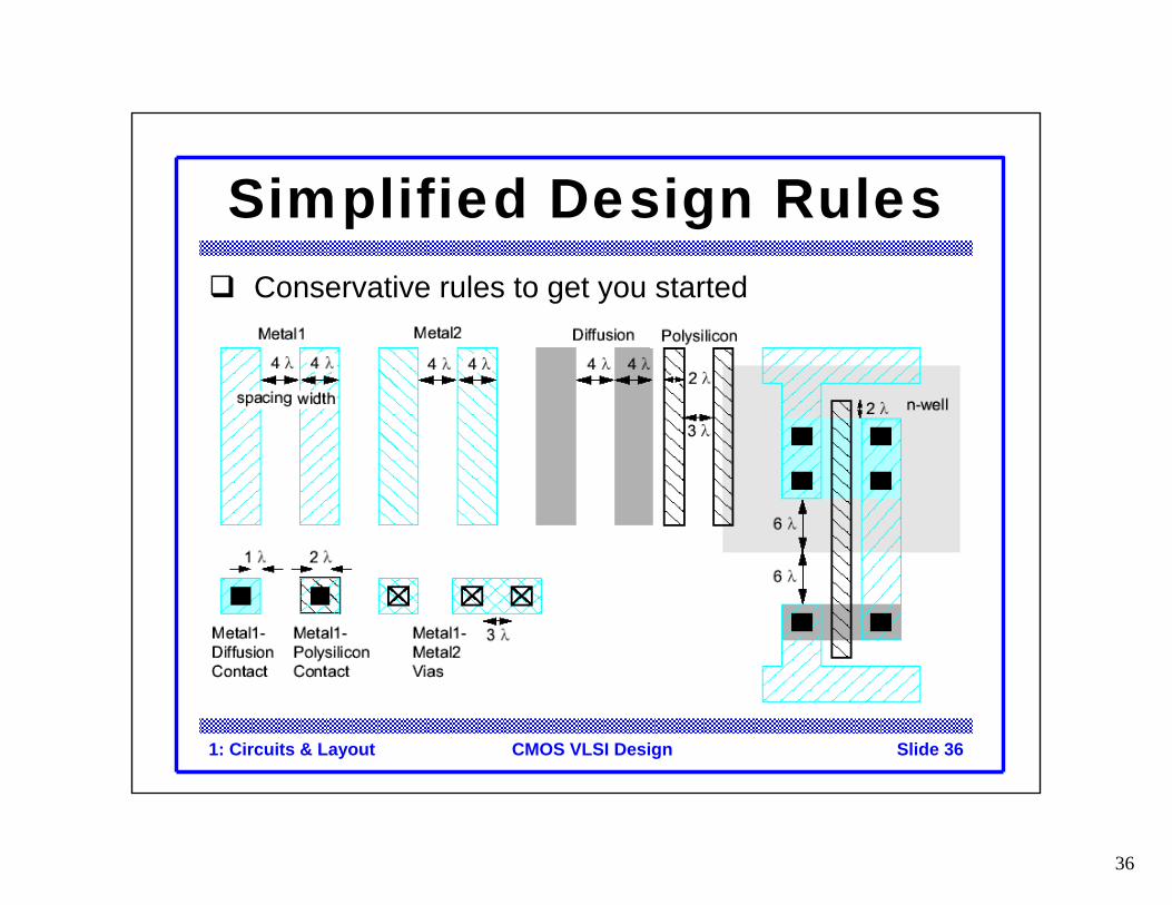
Simplified Design RulesConservative rules to get you started
37
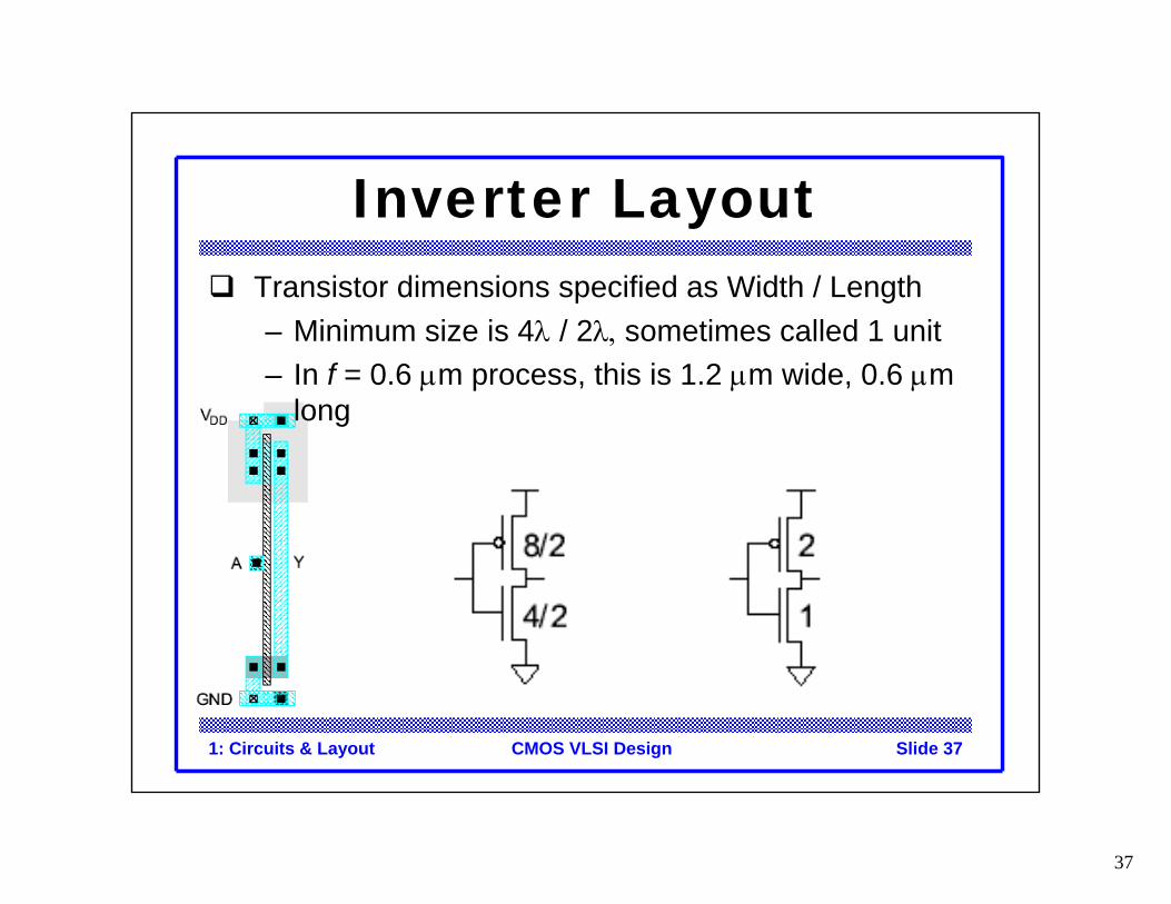
1: Circuits & Layout Slide 37CMOS VLSI Design
Inverter LayoutTransistor dimensions specified as Width / Length– Minimum size is 4λ / 2λ, sometimes called 1 unit– In f = 0.6 μm process, this is 1.2 μm wide, 0.6 μm
long
38
EE14138
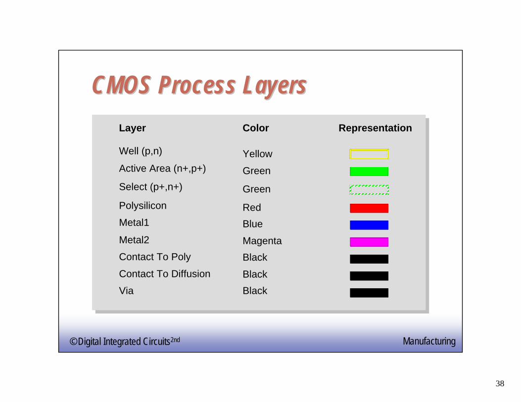
© Digital Integrated Circuits2nd Manufacturing
CMOS Process LayersCMOS Process LayersLayer
Polysilicon
Metal1
Metal2
Contact To Poly
Contact To Diffusion
Via
Well (p,n)
Active Area (n+,p+)
Color Representation
Yellow
Green
RedBlue
MagentaBlack
BlackBlack
Select (p+,n+) Green
39
EE14139
© Digital Integrated Circuits2nd Manufacturing
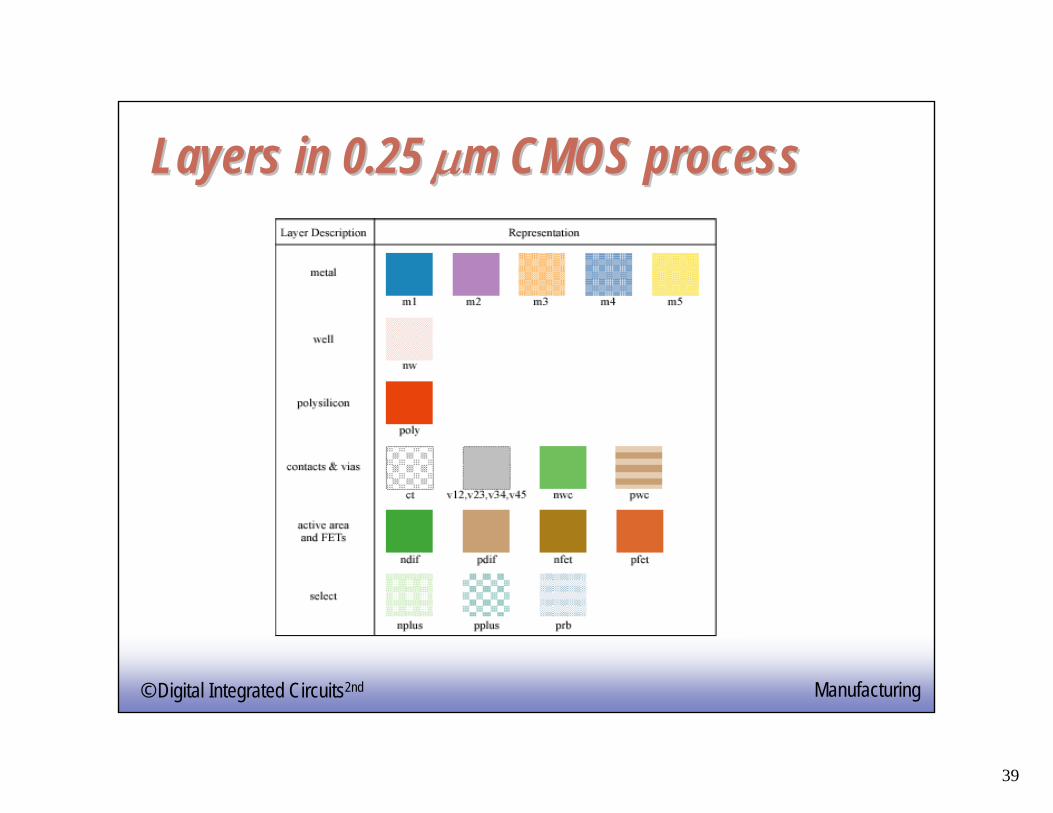
Layers in 0.25 Layers in 0.25 μμm CMOS processm CMOS process
40
EE14140
© Digital Integrated Circuits2nd Manufacturing
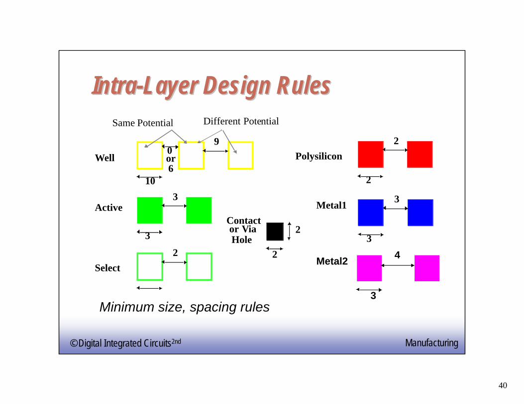
IntraIntra--Layer Design RulesLayer Design Rules
Metal2 4
3
10
90
Well
Active3
3
Polysilicon2
2
Different PotentialSame Potential
Metal1 3
32
Contactor Via
Select2
or6
2Hole
Minimum size, spacing rules

41
EE14141
© Digital Integrated Circuits2nd Manufacturing
Transistor Layout (inter layer rules)Transistor Layout (inter layer rules)
1
2
5
3
Tran
sist
or
42
EE14142
© Digital Integrated Circuits2nd Manufacturing
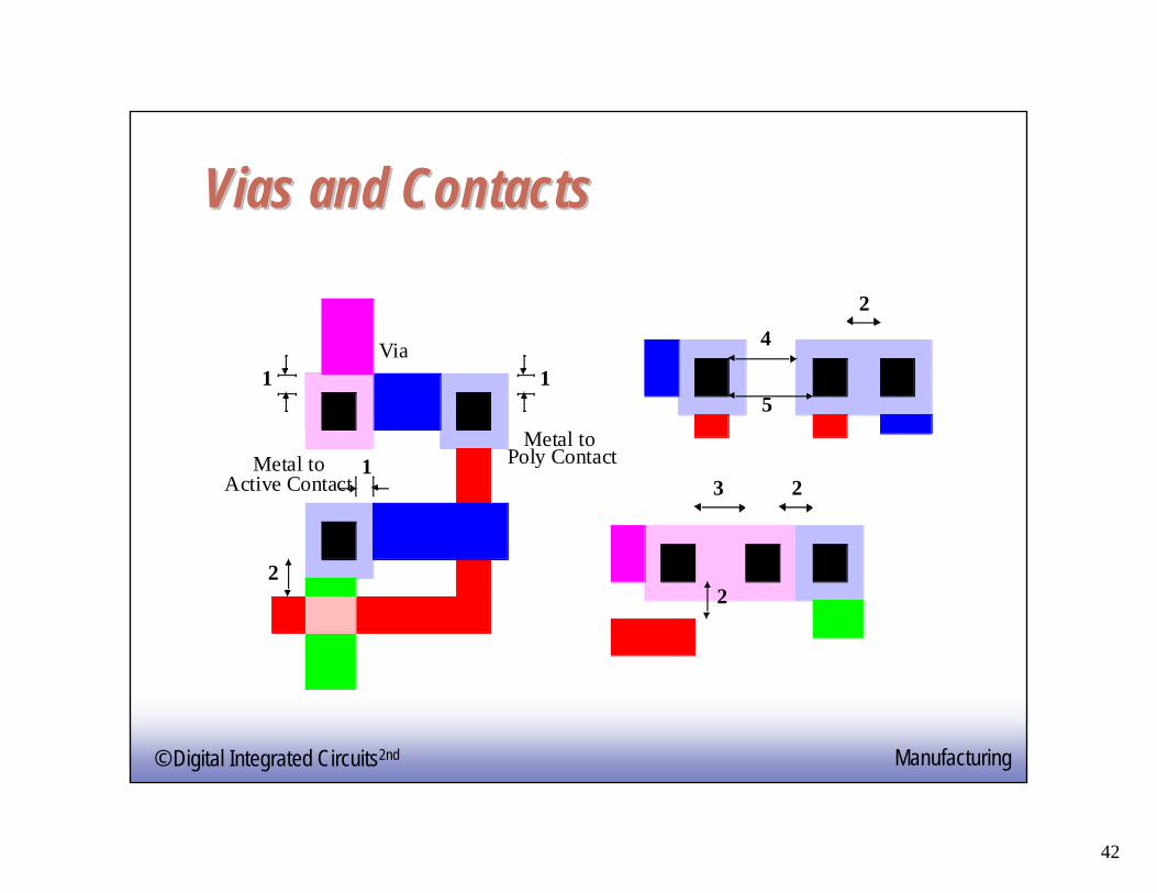
ViasVias and Contactsand Contacts
1
2
1
Via
Metal toPoly ContactMetal to
Active Contact
1
2
5
4
3 2
2
43
EE14143
© Digital Integrated Circuits2nd Manufacturing
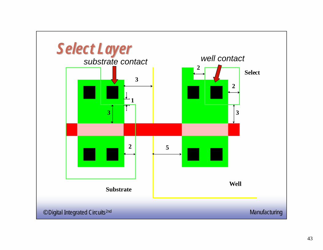
Select LayerSelect Layer
1
3 3
2
2
2
WellSubstrate
Select3
5
well contactsubstrate contact
44
EE14144
© Digital Integrated Circuits2nd Manufacturing
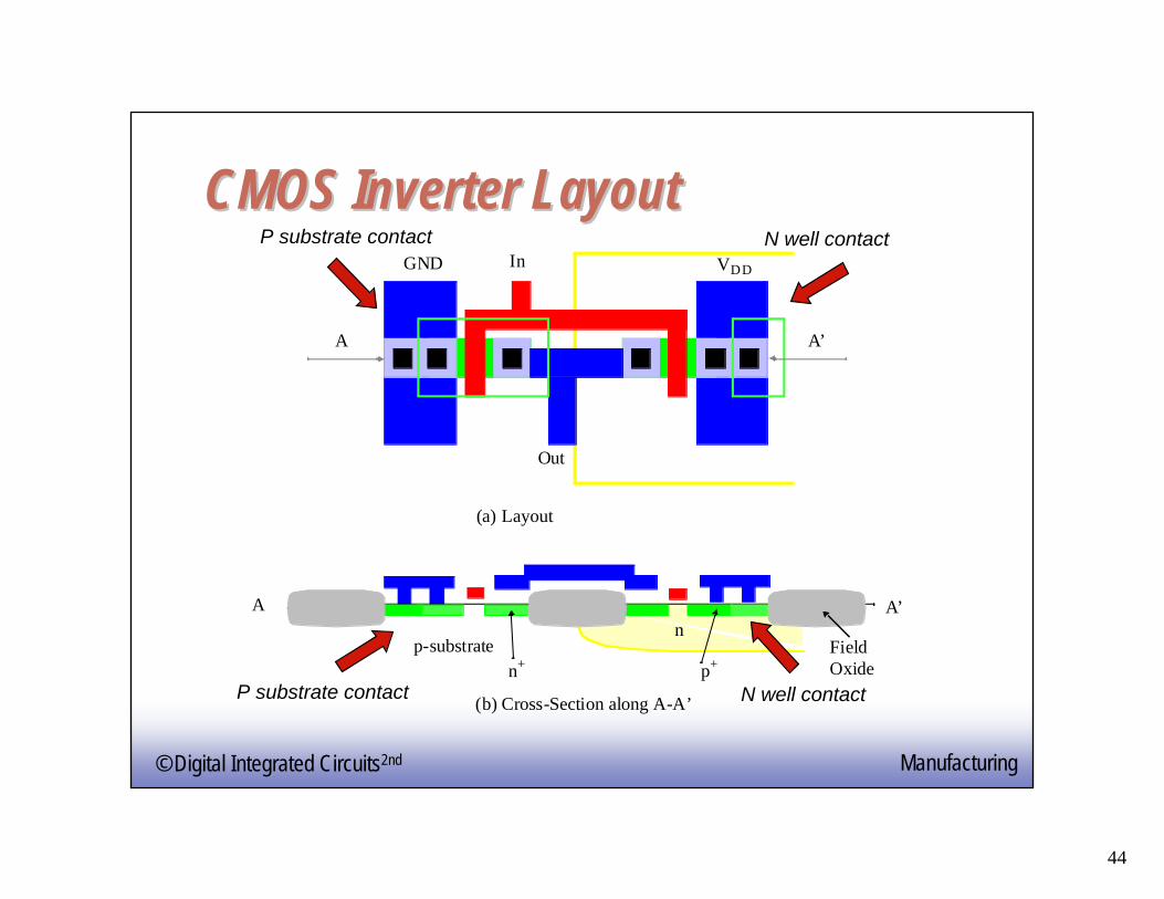
CMOS Inverter LayoutCMOS Inverter Layout
A A’
np-substrate Field
Oxidep+n+
In
Out
GND VDD
(a) Layout
(b) Cross-Section along A-A’
A A’
N well contactP substrate contact
N well contactP substrate contact
45
EE14145
© Digital Integrated Circuits2nd Manufacturing
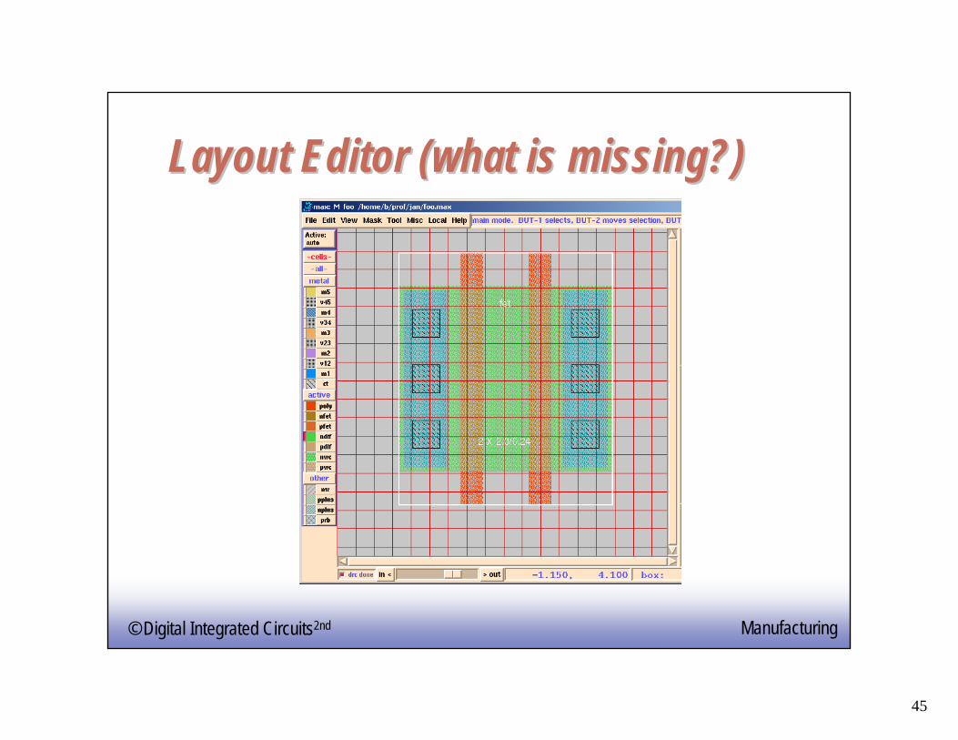
Layout Editor (what is missing?)Layout Editor (what is missing?)
46
EE14146
© Digital Integrated Circuits2nd Manufacturing
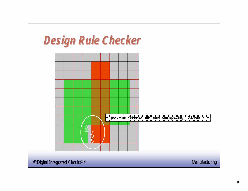
Design Rule CheckerDesign Rule Checker
poly_not_fet to all_diff minimum spacing = 0.14 um.
47
EE14147
© Digital Integrated Circuits2nd Manufacturing
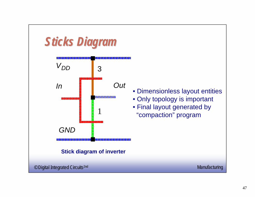
Sticks DiagramSticks Diagram
1
3
In Out
VDD
GND
Stick diagram of inverter
• Dimensionless layout entities• Only topology is important• Final layout generated by “compaction” program
48
1: Circuits & Layout Slide 48CMOS VLSI Design
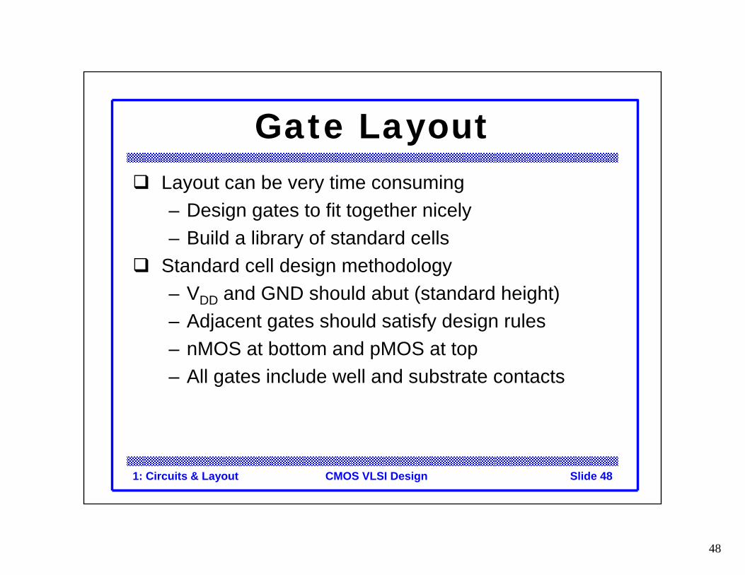
Gate LayoutLayout can be very time consuming– Design gates to fit together nicely– Build a library of standard cells
Standard cell design methodology– VDD and GND should abut (standard height)– Adjacent gates should satisfy design rules– nMOS at bottom and pMOS at top– All gates include well and substrate contacts
49
1: Circuits & Layout Slide 49CMOS VLSI Design
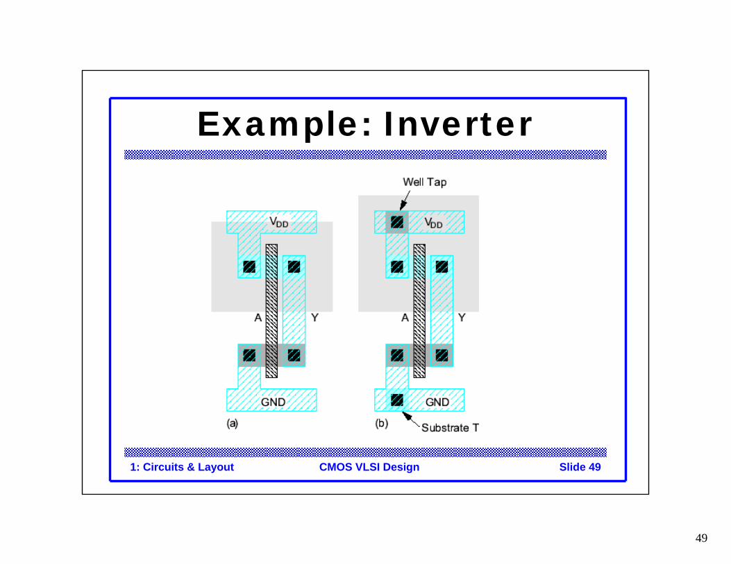
Example: Inverter
50
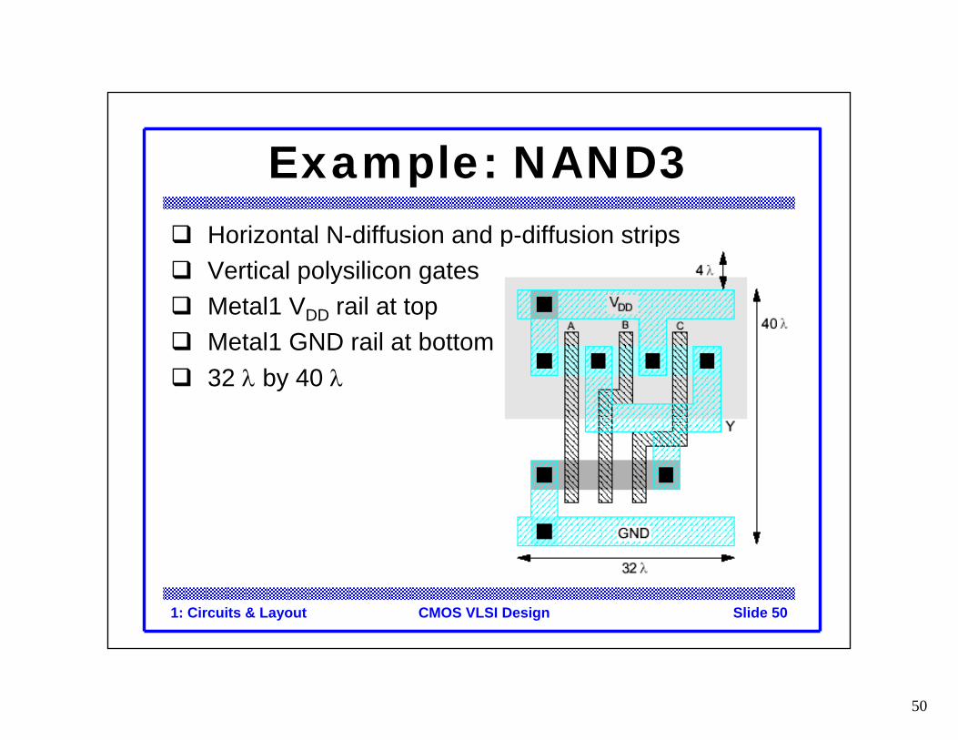
1: Circuits & Layout Slide 50CMOS VLSI Design
Example: NAND3Horizontal N-diffusion and p-diffusion stripsVertical polysilicon gatesMetal1 VDD rail at topMetal1 GND rail at bottom32 λ by 40 λ
51
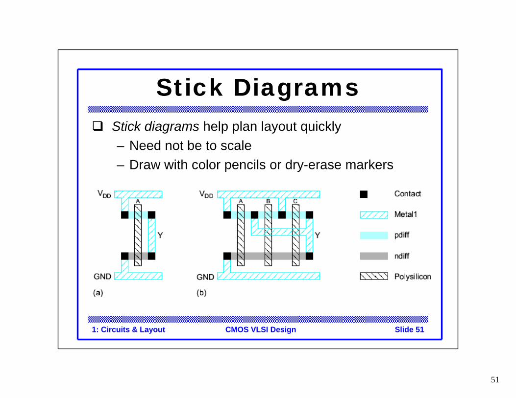
1: Circuits & Layout Slide 51CMOS VLSI Design
Stick DiagramsStick diagrams help plan layout quickly– Need not be to scale– Draw with color pencils or dry-erase markers
52
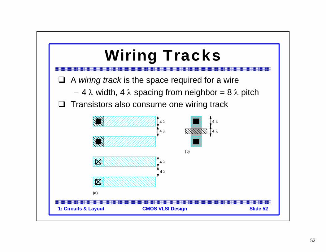
1: Circuits & Layout Slide 52CMOS VLSI Design
Wiring TracksA wiring track is the space required for a wire– 4 λ width, 4 λ spacing from neighbor = 8 λ pitch
Transistors also consume one wiring track
53
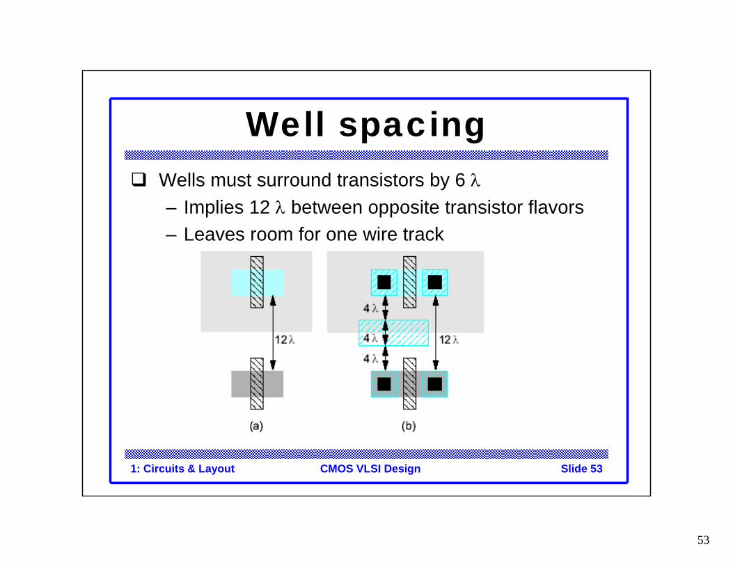
1: Circuits & Layout Slide 53CMOS VLSI Design
Well spacingWells must surround transistors by 6 λ– Implies 12 λ between opposite transistor flavors– Leaves room for one wire track
54
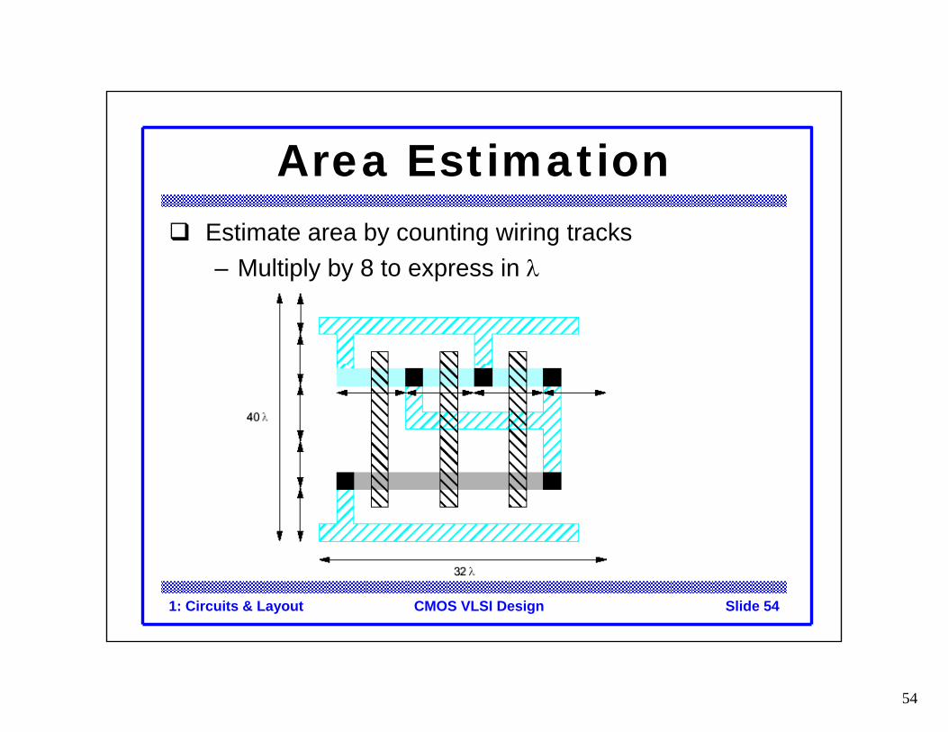
1: Circuits & Layout Slide 54CMOS VLSI Design
Area EstimationEstimate area by counting wiring tracks– Multiply by 8 to express in λ
55
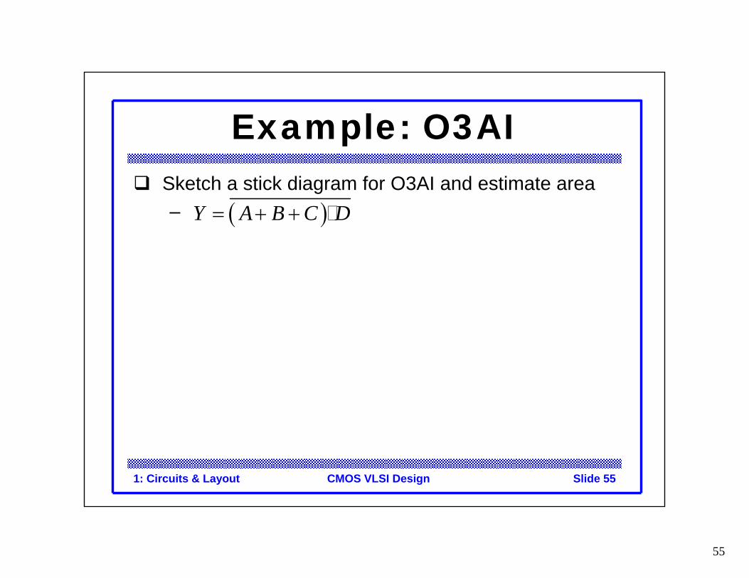
1: Circuits & Layout Slide 55CMOS VLSI Design
Example: O3AISketch a stick diagram for O3AI and estimate area– ( )Y A B C D= + +
56
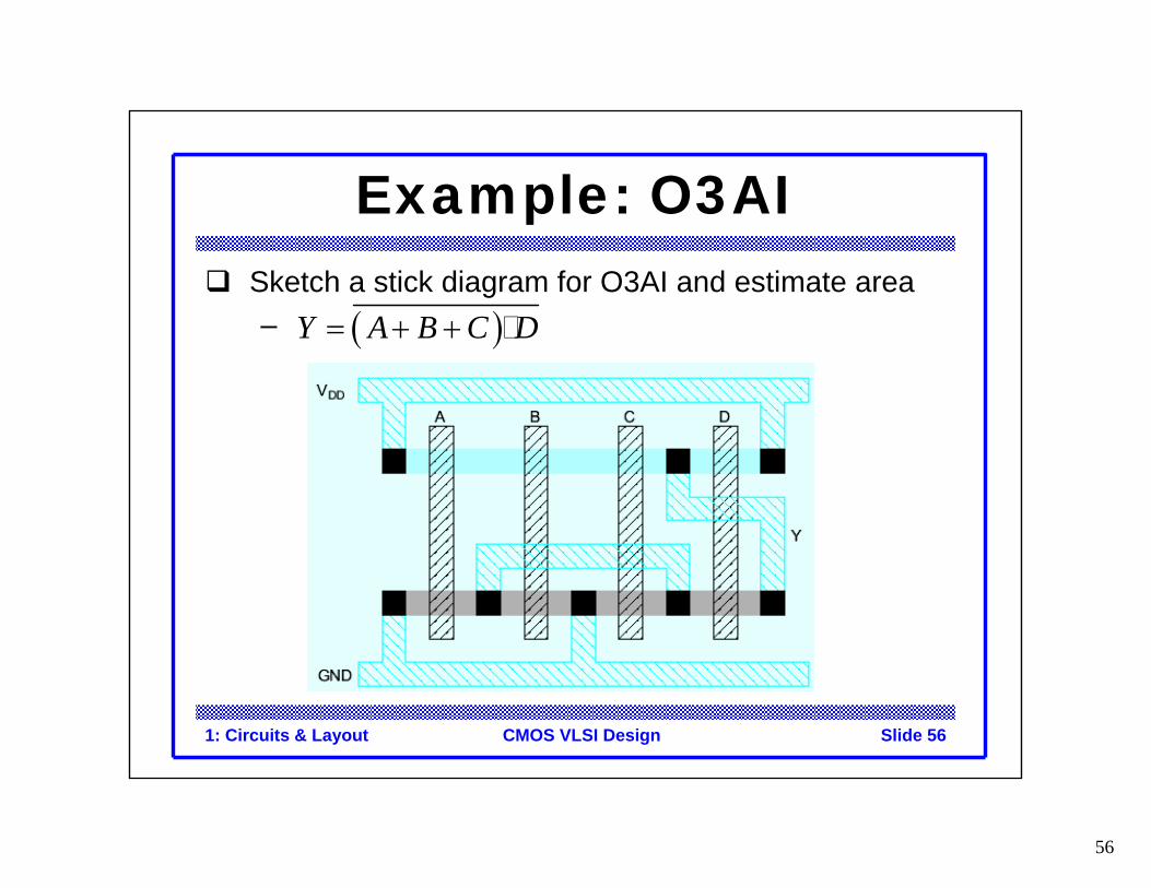
1: Circuits & Layout Slide 56CMOS VLSI Design
Example: O3AISketch a stick diagram for O3AI and estimate area– ( )Y A B C D= + +
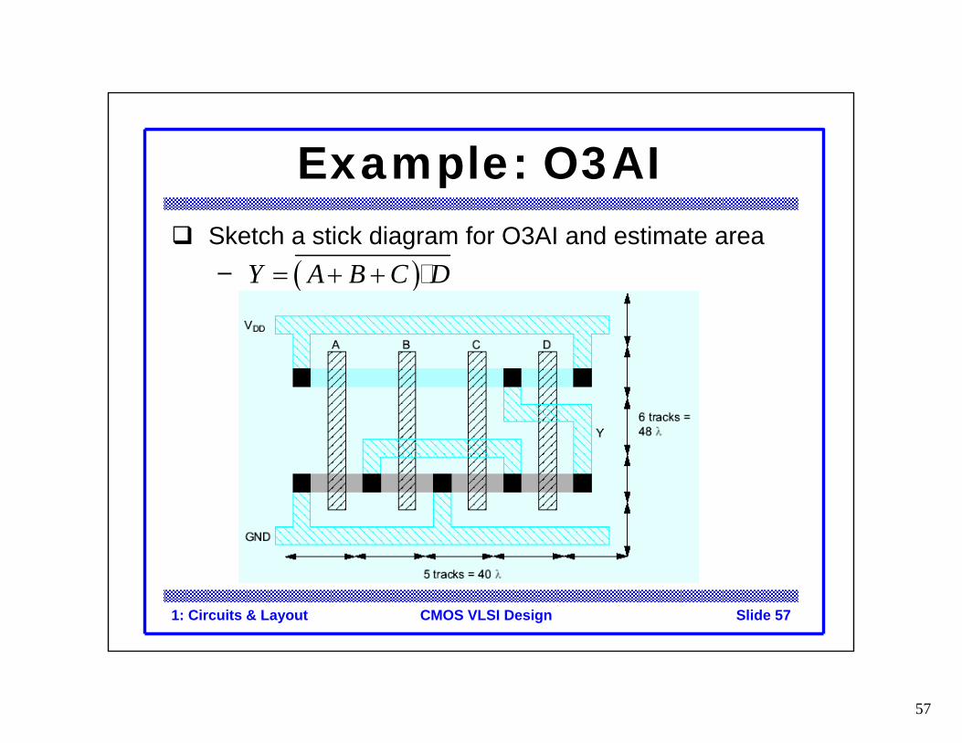
57
1: Circuits & Layout Slide 57CMOS VLSI Design
Example: O3AISketch a stick diagram for O3AI and estimate area– ( )Y A B C D= + +