LC Oscillators – Lower RF Frequencieshome.sandiego.edu/~ekim/e194rfs01/lec25ek.pdf · •...
25
Basic Oscillator Model • Oscillator has positive feedback loop at selected frequency • Barkhausen criteria implies that the multiplication of the transfer functions of open loop amplifier and feedback stage is H F (ω)H A (ω) = 1 • Barkhausen criteria aka loop gain equation
Transcript of LC Oscillators – Lower RF Frequencieshome.sandiego.edu/~ekim/e194rfs01/lec25ek.pdf · •...
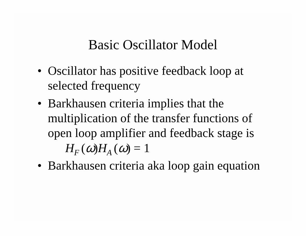
Basic Oscillator Model
• Oscillator has positive feedback loop at selected frequency
• Barkhausen criteria implies that the multiplication of the transfer functions of open loop amplifier and feedback stage is
HF (ω)HA (ω) = 1• Barkhausen criteria aka loop gain equation
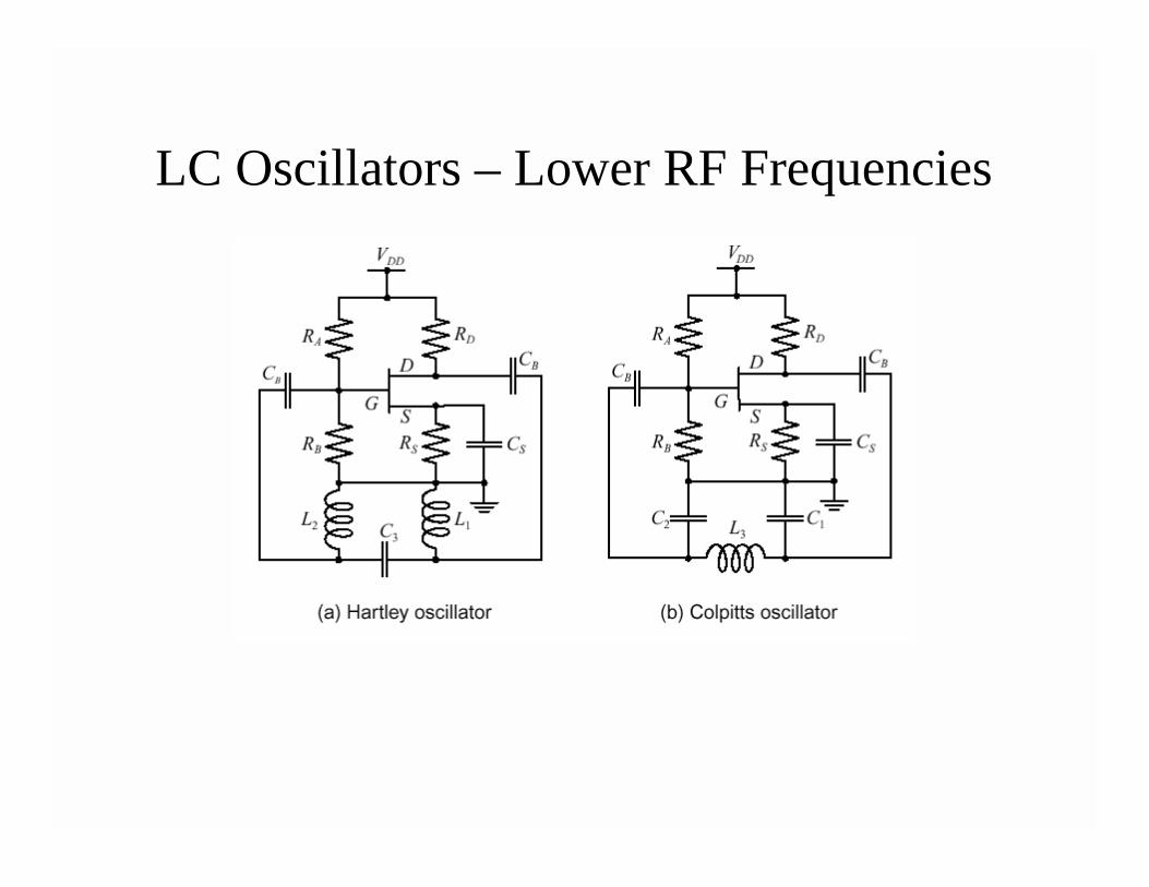
LC Oscillators – Lower RF Frequencies
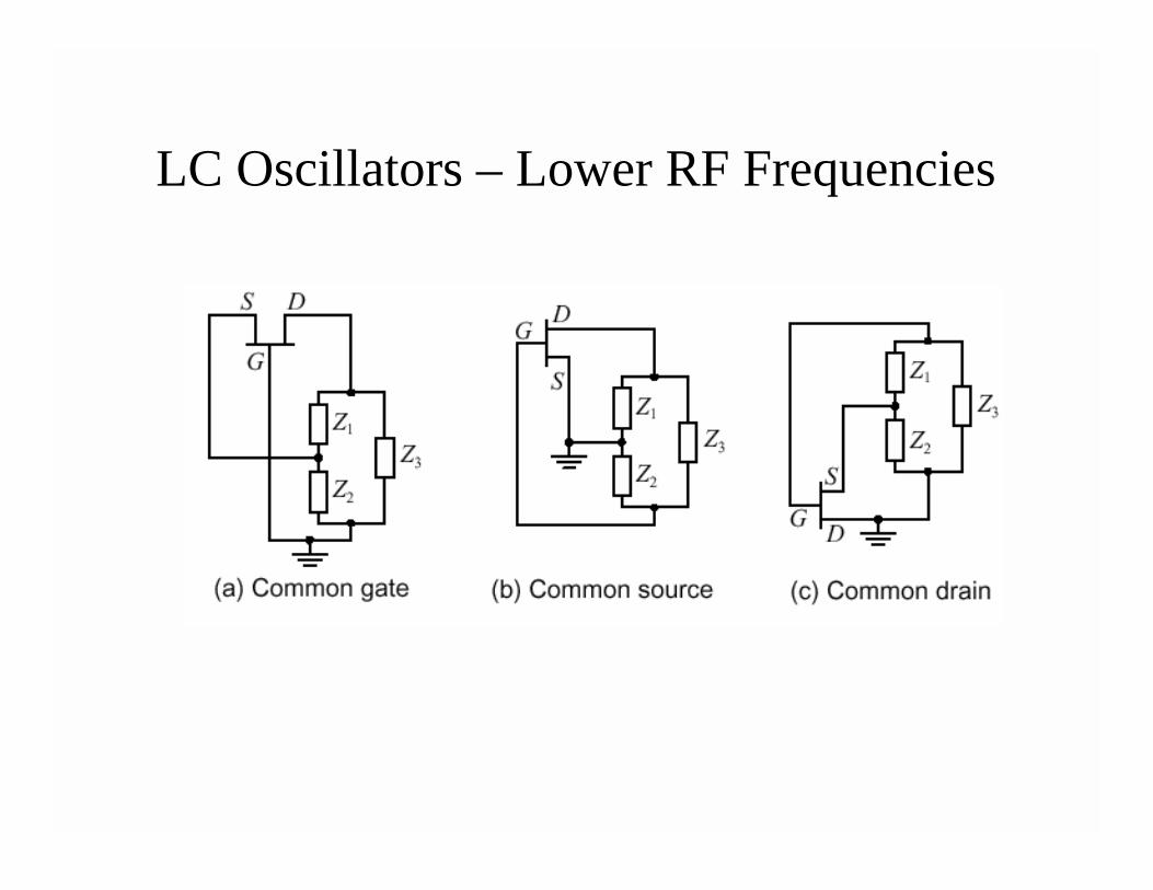
LC Oscillators – Lower RF Frequencies
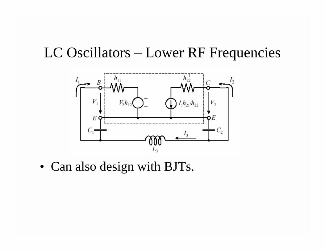
LC Oscillators – Lower RF Frequencies
• Can also design with BJTs.

High RF & Microwave Oscillators
• Take advantage of our knowledge of stability
• Rollett Stability Factor k < 1
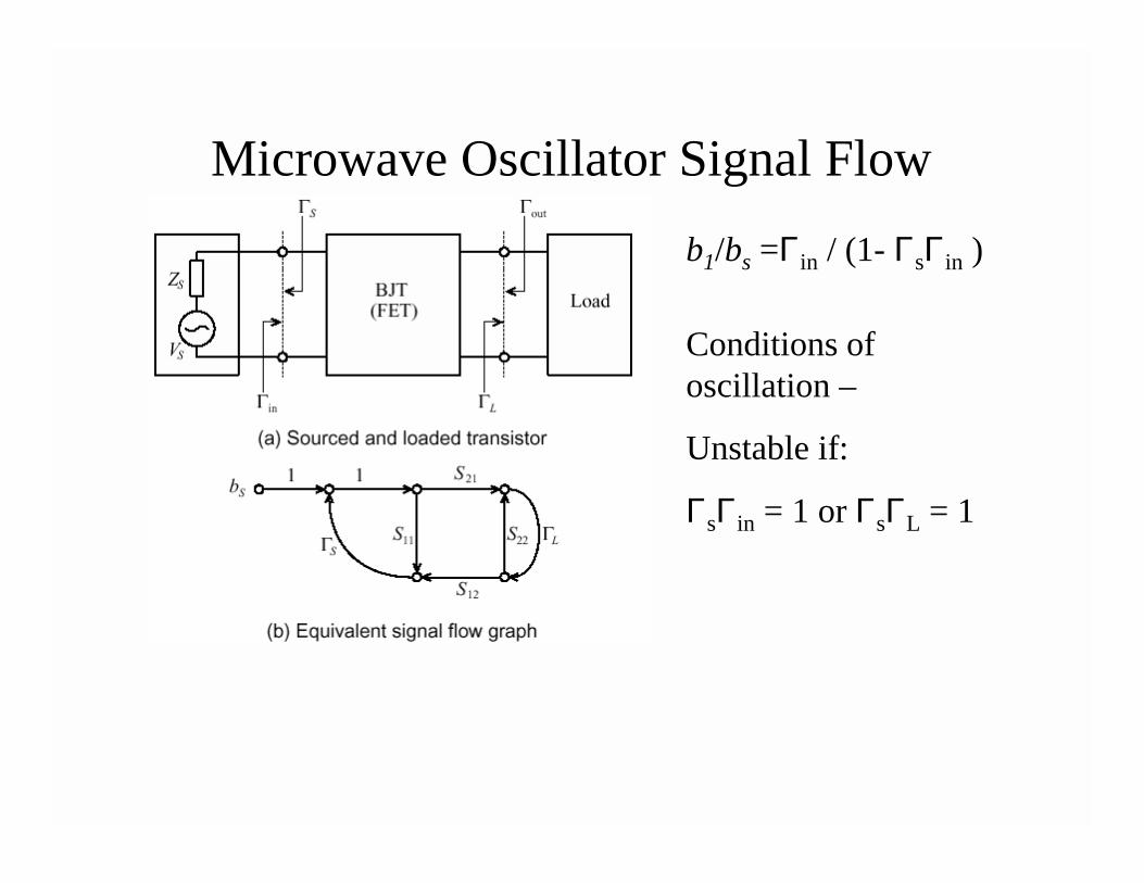
Microwave Oscillator Signal Flowb1/bs =Γin / (1- ΓsΓin )
Conditions of oscillation –
Unstable if:
ΓsΓin = 1 or ΓsΓL = 1
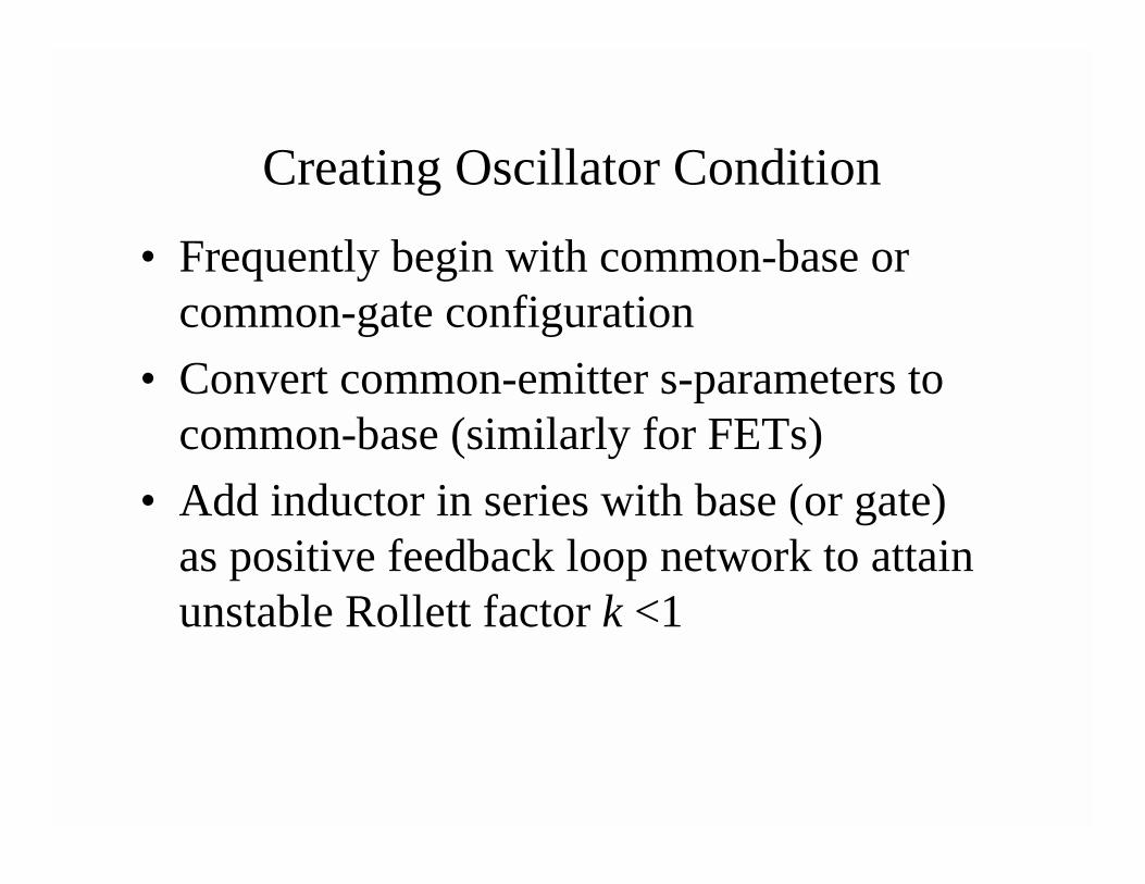
Creating Oscillator Condition
• Frequently begin with common-base or common-gate configuration
• Convert common-emitter s-parameters to common-base (similarly for FETs)
• Add inductor in series with base (or gate) as positive feedback loop network to attain unstable Rollett factor k <1
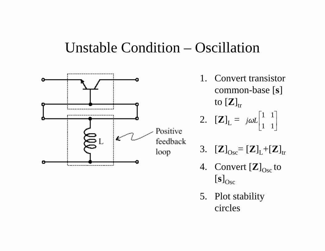
Unstable Condition – Oscillation
1. Convert transistor common-base [s] to [Z]tr
2. [Z]L =
3. [Z]Osc= [Z]L+[Z]tr
4. Convert [Z]Osc to [s]Osc
5. Plot stability circles
1 11 1
j Lω
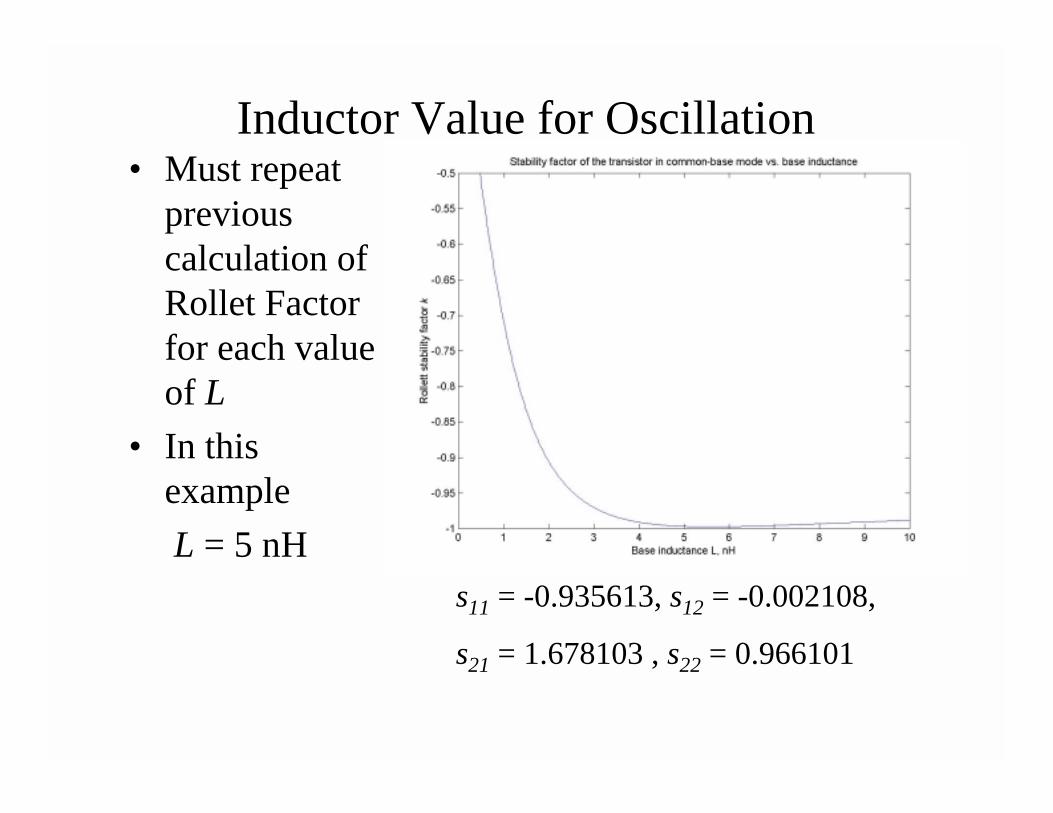
Inductor Value for Oscillation• Must repeat
previous calculation ofRollet Factor for each value of L
• In this exampleL = 5 nH
s11 = -0.935613, s12 = -0.002108,
s21 = 1.678103 , s22 = 0.966101
Unstable Transistor Oscillator Design1. Select potentially unstable transistor at freq2. Select appropriate transistor configuration3. Draw output stability circle in ΓL plane4. Select appropriate value of ΓL to produce largest
possible negative resistance at input of transistor yielding |ΓL | >1 and Zin < 0
5. Select source tuning impedance Zs as if the circuit was a one-port oscillator by RS + RIN < 0 typically RS = |RIN|/3, RIN < 0 and XS = -XIN
6. Design source tuning and terminating networks with lumped or distributed elements
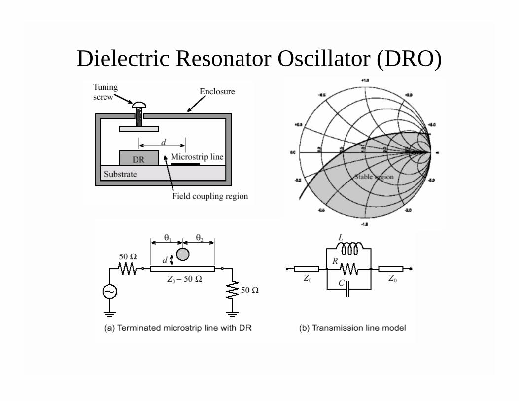
Dielectric Resonator Oscillator (DRO)
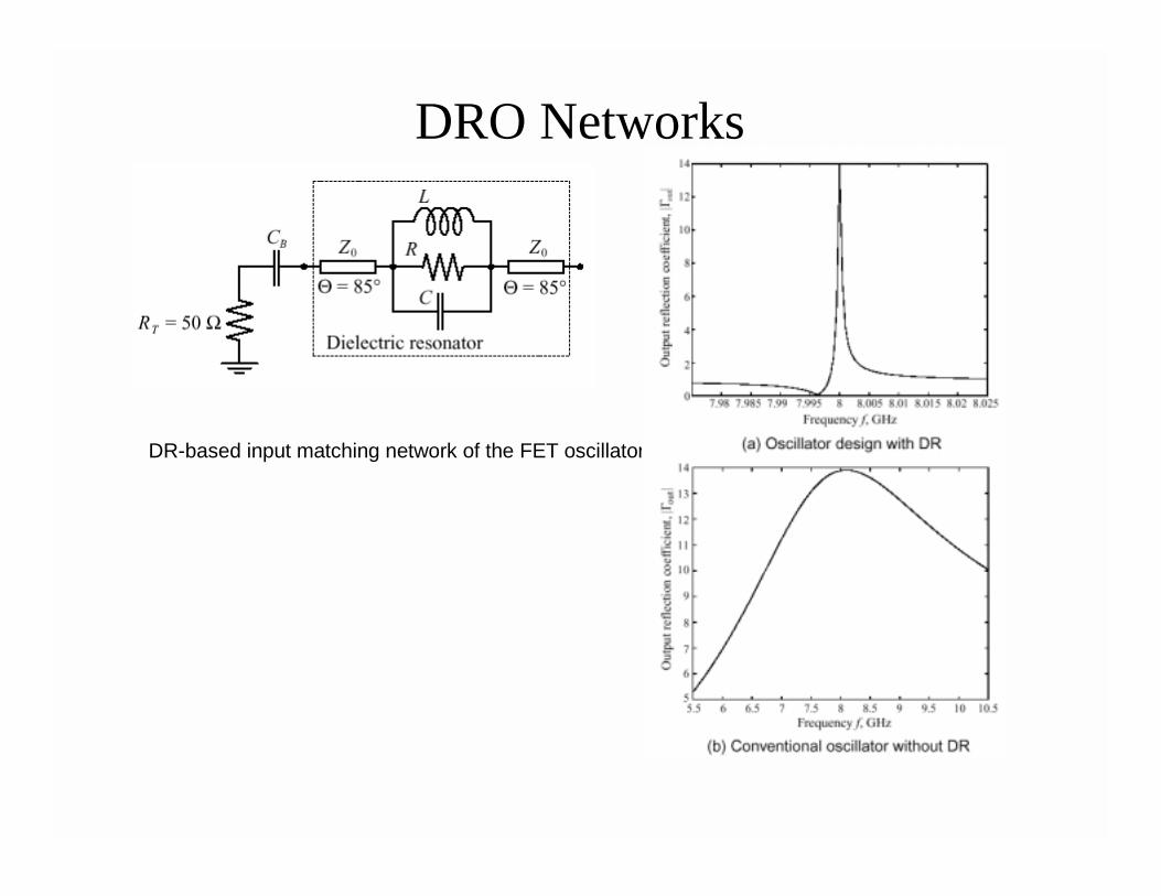
DRO Networks
DR-based input matching network of the FET oscillator.
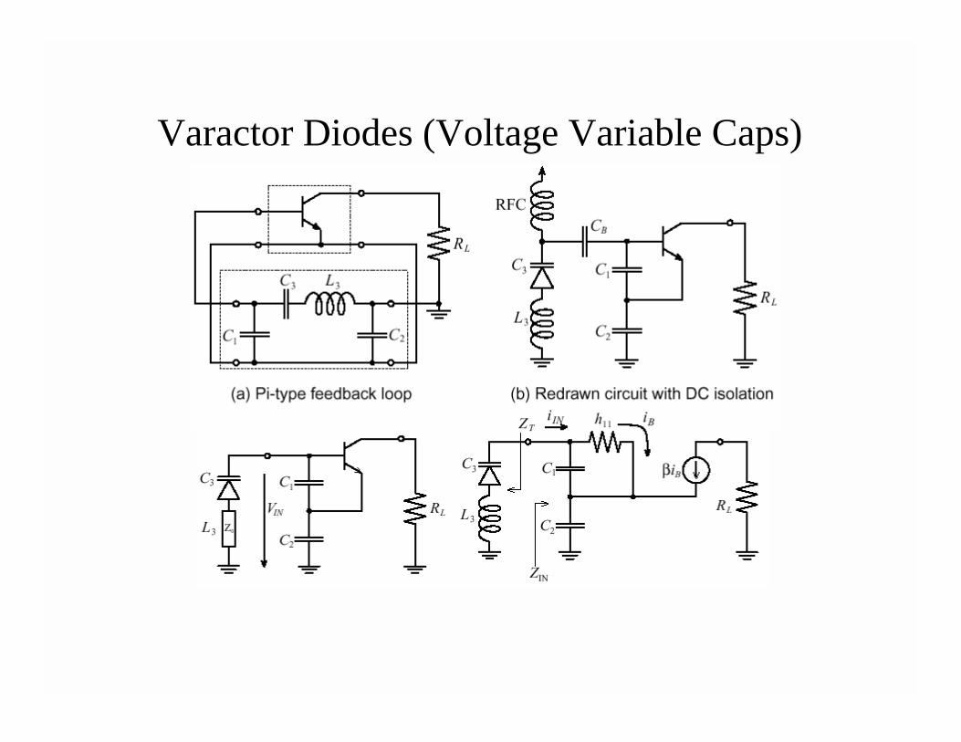
Varactor Diodes (Voltage Variable Caps)
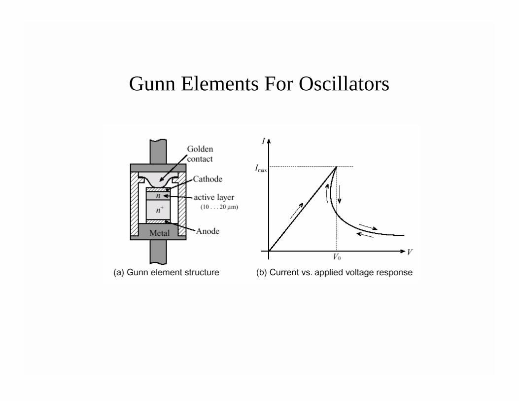
Gunn Elements For Oscillators
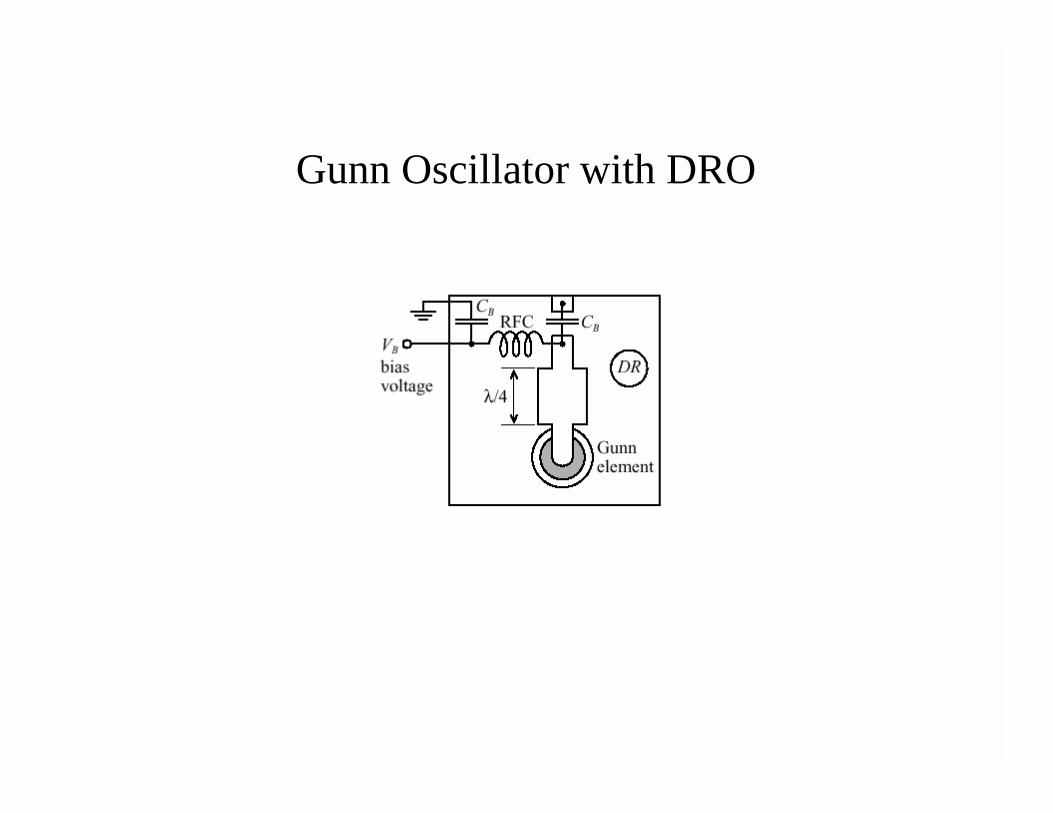
Gunn Oscillator with DRO
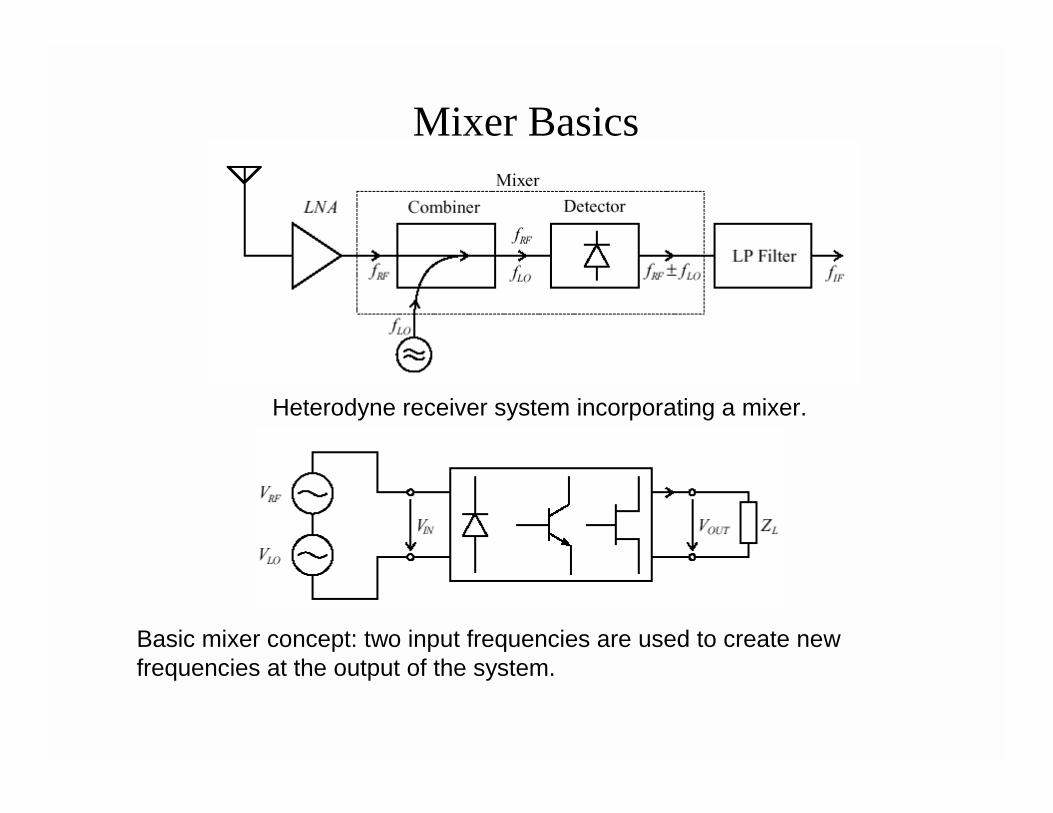
Mixer Basics
Heterodyne receiver system incorporating a mixer.
Basic mixer concept: two input frequencies are used to create new frequencies at the output of the system.
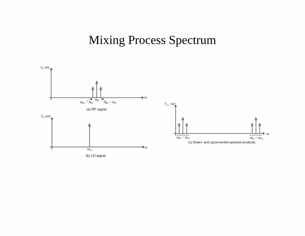
Mixing Process Spectrum
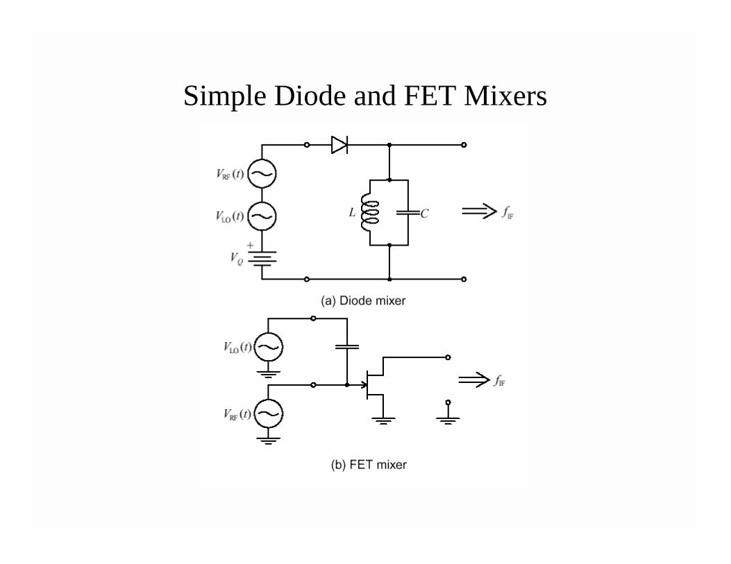
Simple Diode and FET Mixers
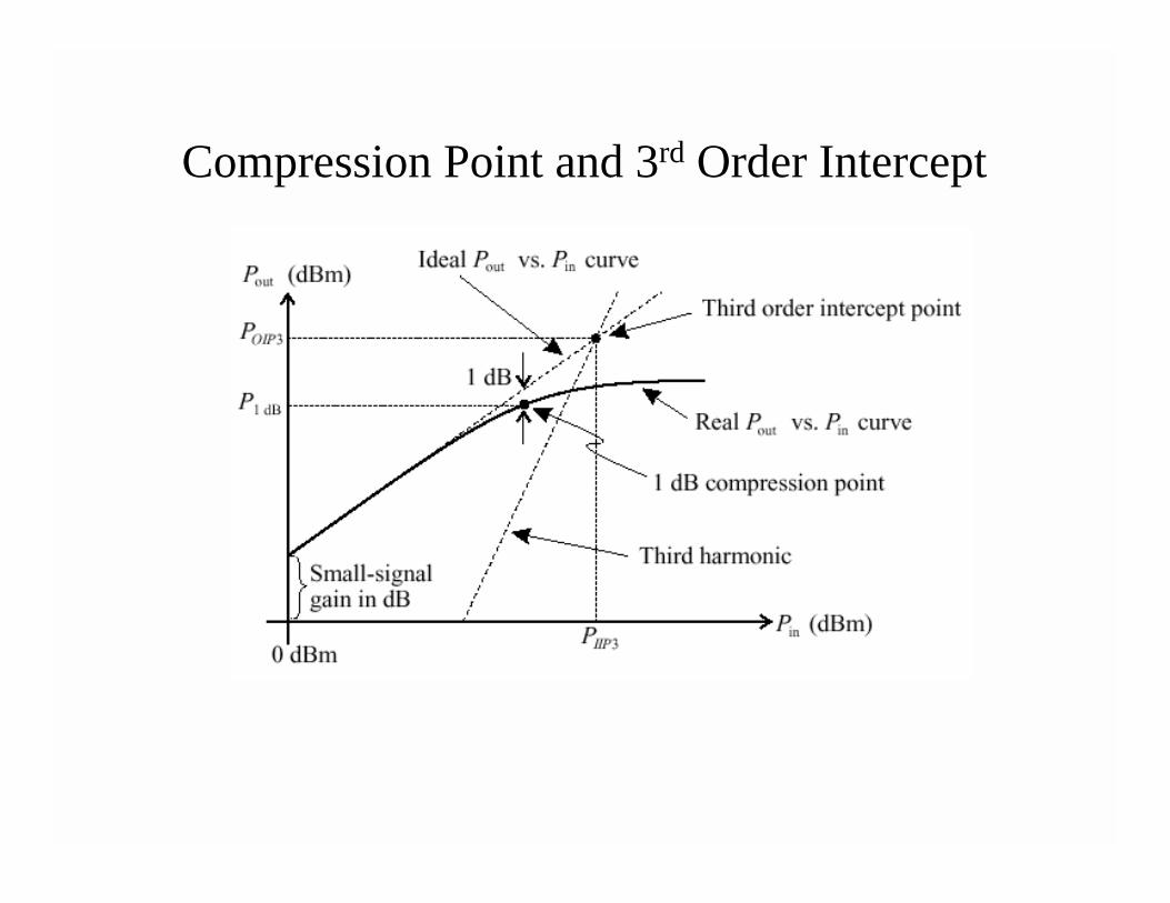
Compression Point and 3rd Order Intercept
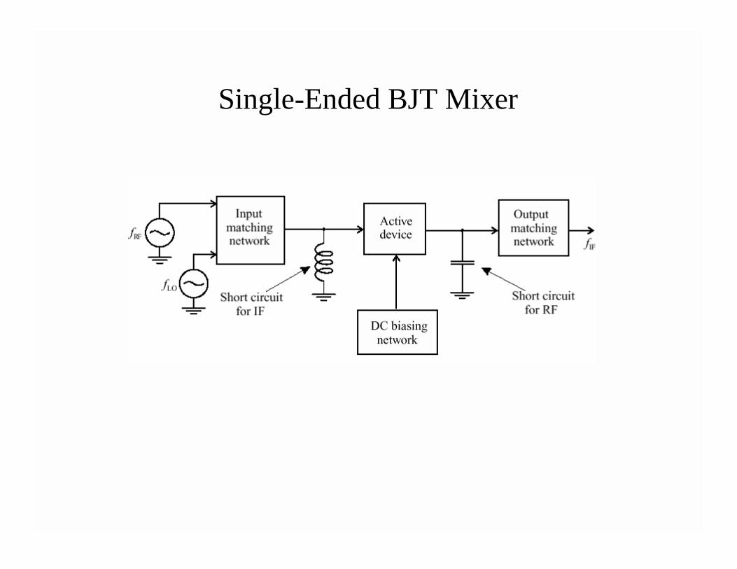
Single-Ended BJT Mixer
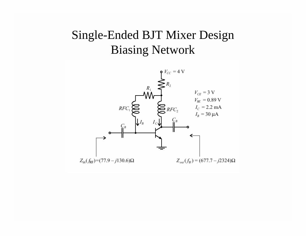
Single-Ended BJT Mixer Design Biasing Network
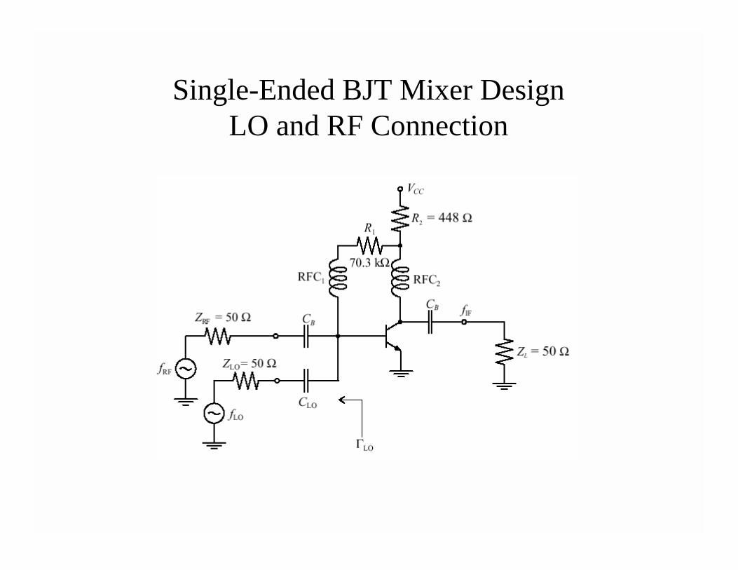
Single-Ended BJT Mixer DesignLO and RF Connection
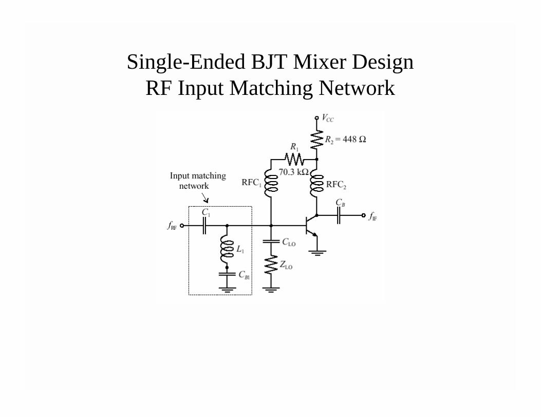
Single-Ended BJT Mixer DesignRF Input Matching Network
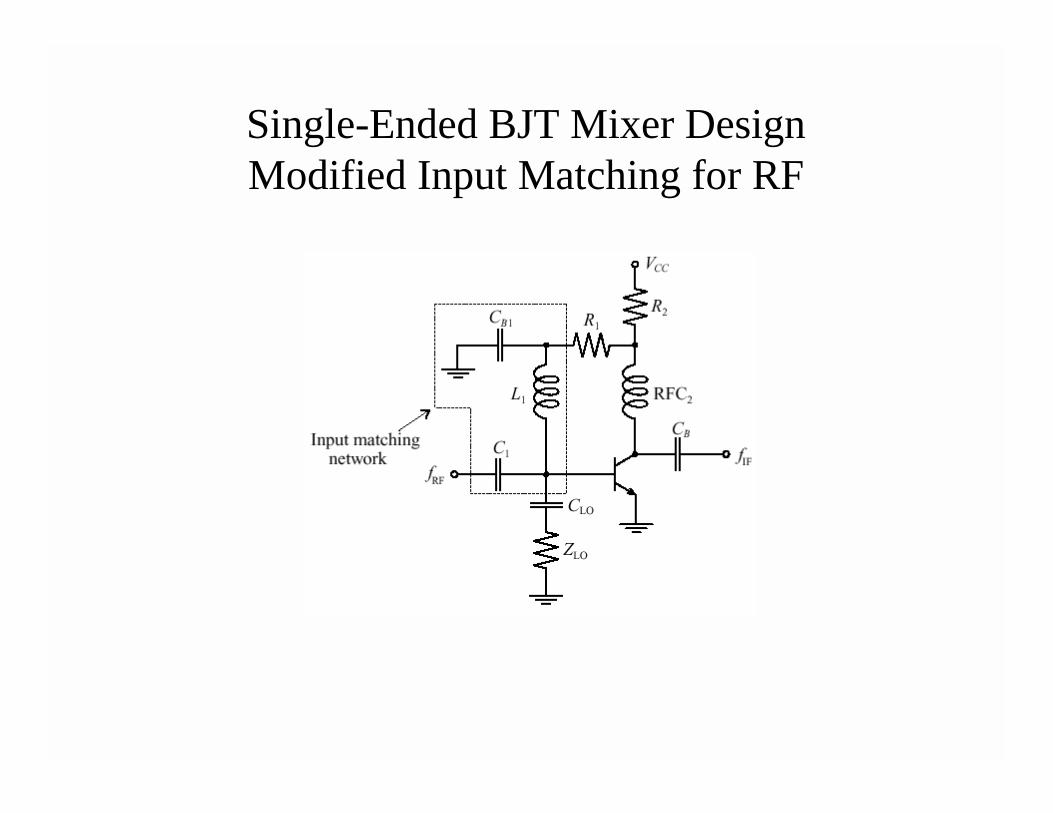
Single-Ended BJT Mixer DesignModified Input Matching for RF
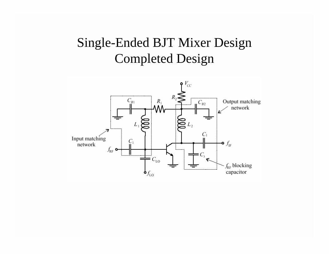
Single-Ended BJT Mixer DesignCompleted Design


![SITRANS F C MASSFLO - Siemens · SITRANS F C MASSFLO ... 50 50 50 50 50 50 50 50 Equivalent cable must have Lc/Rc ratio lower or equal to 100 [µh/Ω]. SITRANS F C MASSFLO ...](https://static.fdocument.org/doc/165x107/5add07b37f8b9aa5088c4cf1/sitrans-f-c-massflo-siemens-f-c-massflo-50-50-50-50-50-50-50-50-equivalent.jpg)