Introduction to Molecular Electronics2010...
35
Introduction to Molecular Electronics Lecture 2
Transcript of Introduction to Molecular Electronics2010...
Introduction to Molecular
Electronics
Lecture 2
Scope
• Electronic energy levels in a molecule: electronic structure of a π-conjugated system
• Designing Molecular building blocks
• Molecular Electronics with Scanning probe techniques (continued in the paperpresentation)
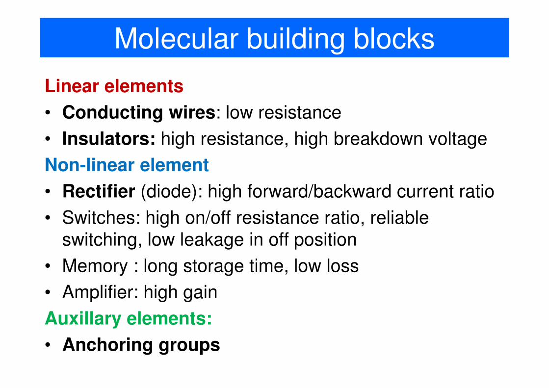
Molecular building blocks
Linear elements
• Conducting wires: low resistance
• Insulators: high resistance, high breakdown voltage
Non-linear element
• Rectifier (diode): high forward/backward current ratio
• Switches: high on/off resistance ratio, reliable
switching, low leakage in off position
• Memory : long storage time, low loss
• Amplifier: high gain
Auxillary elements:
• Anchoring groups
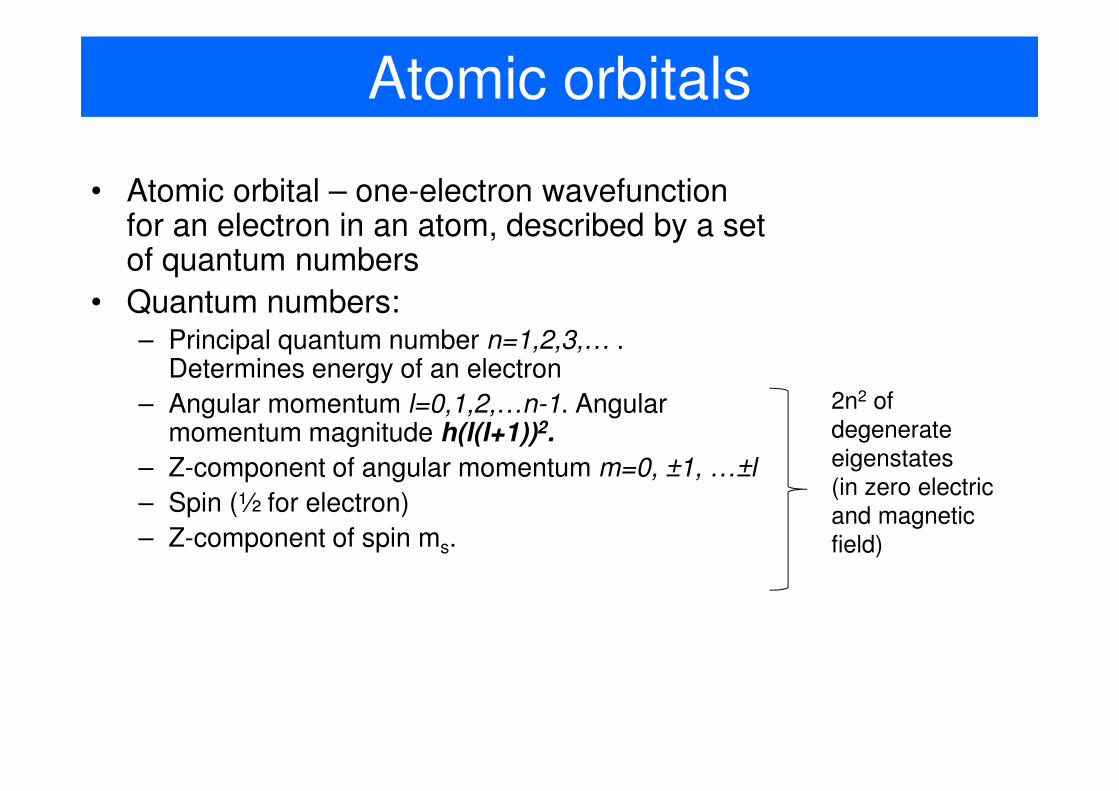
Atomic orbitals
• Atomic orbital – one-electron wavefunctionfor an electron in an atom, described by a set of quantum numbers
• Quantum numbers:– Principal quantum number n=1,2,3,… .
Determines energy of an electron
– Angular momentum l=0,1,2,…n-1. Angular momentum magnitude h(l(l+1))2.
– Z-component of angular momentum m=0, ±1, …±l
– Spin (½ for electron)
– Z-component of spin ms.
2n2 of
degenerate
eigenstates
(in zero electric
and magnetic
field)
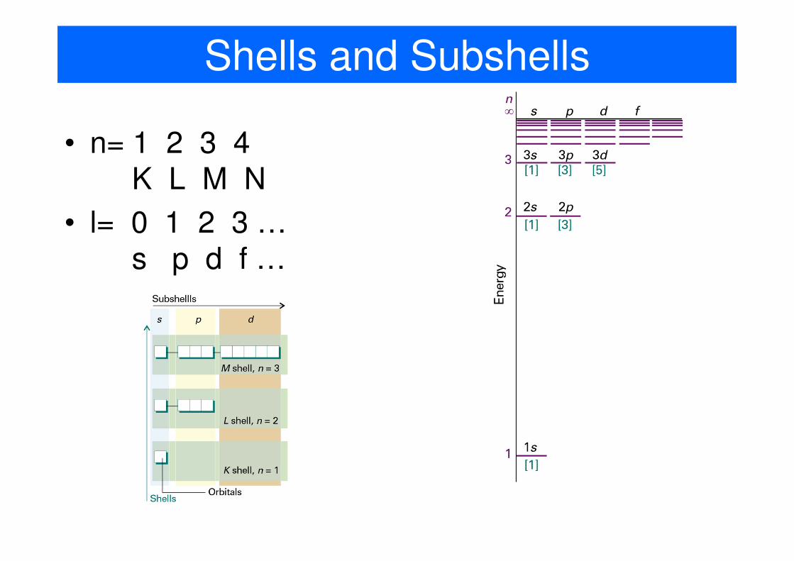
Shells and Subshells
• n= 1 2 3 4K L M N
• l= 0 1 2 3 …s p d f …
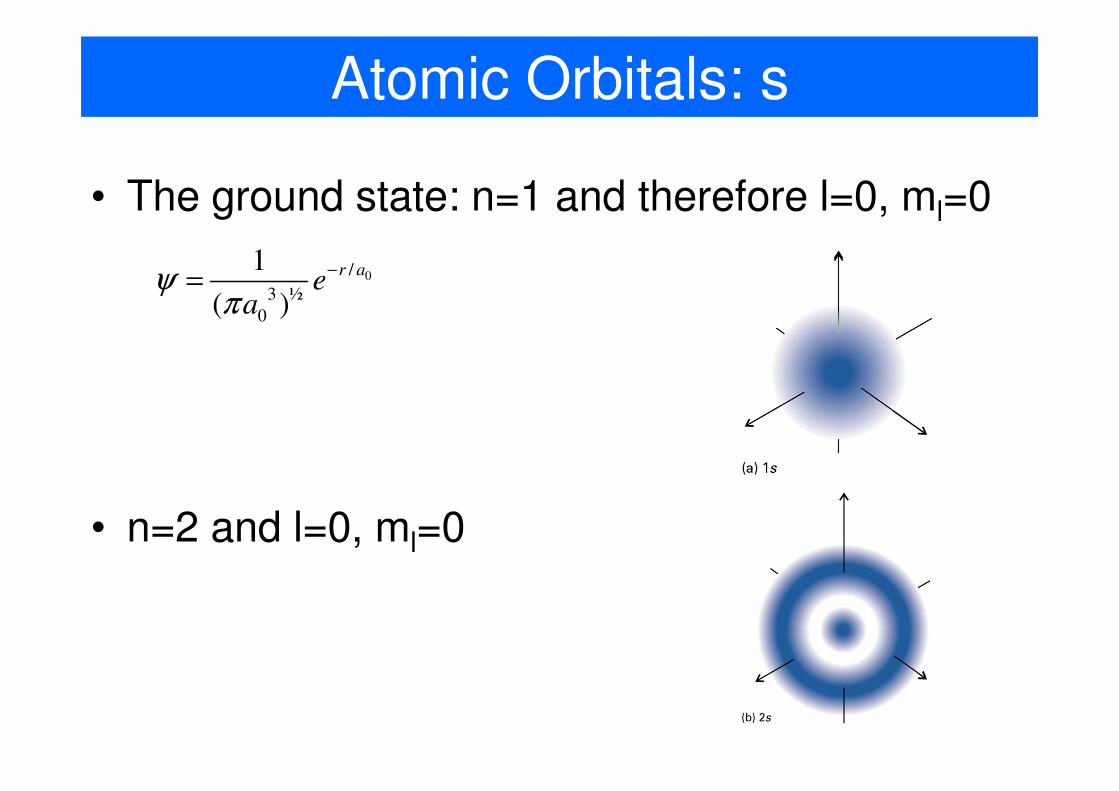
Atomic Orbitals: s
• The ground state: n=1 and therefore l=0, ml=0
0/
3 ½
0
1
( )
r ae
aψ
π−=
• n=2 and l=0, ml=0
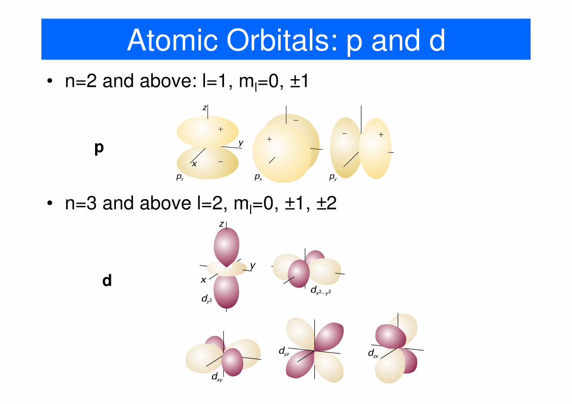
Atomic Orbitals: p and d
p
d
• n=2 and above: l=1, ml=0, ±1
• n=3 and above l=2, ml=0, ±1, ±2
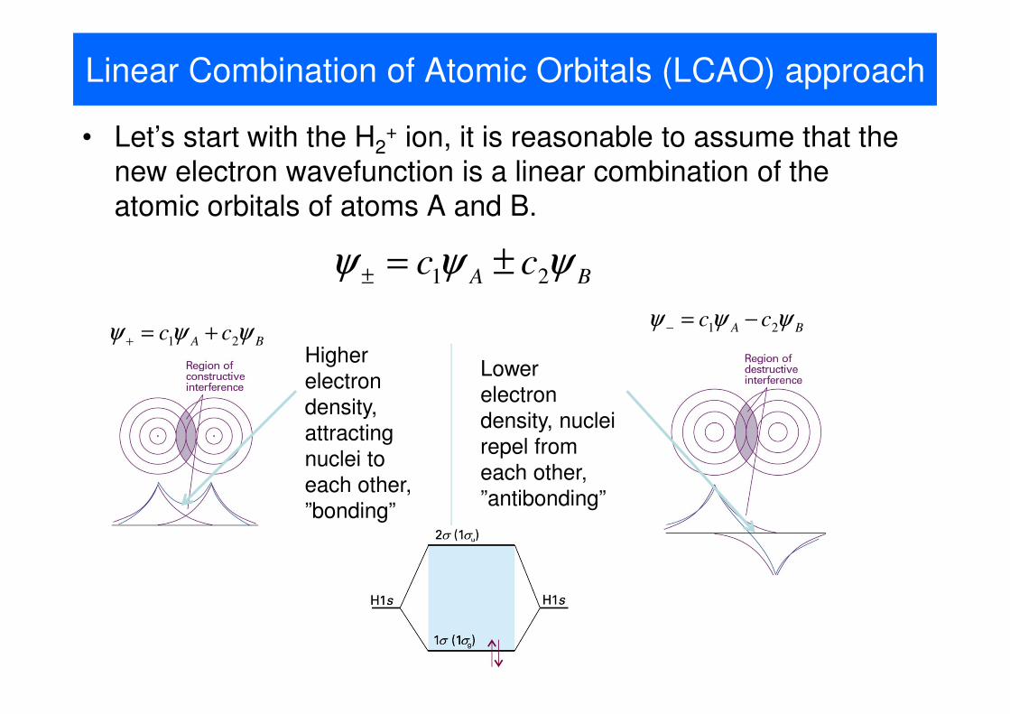
Linear Combination of Atomic Orbitals (LCAO) approach
• Let’s start with the H2+ ion, it is reasonable to assume that the
new electron wavefunction is a linear combination of the
atomic orbitals of atoms A and B.
BA cc ψψψ21
±=±
BA cc ψψψ21
+=+BA cc ψψψ
21−=−
Higher
electron
density,
attracting
nuclei to
each other,
”bonding”
Lower
electron
density, nuclei
repel from
each other,
”antibonding”
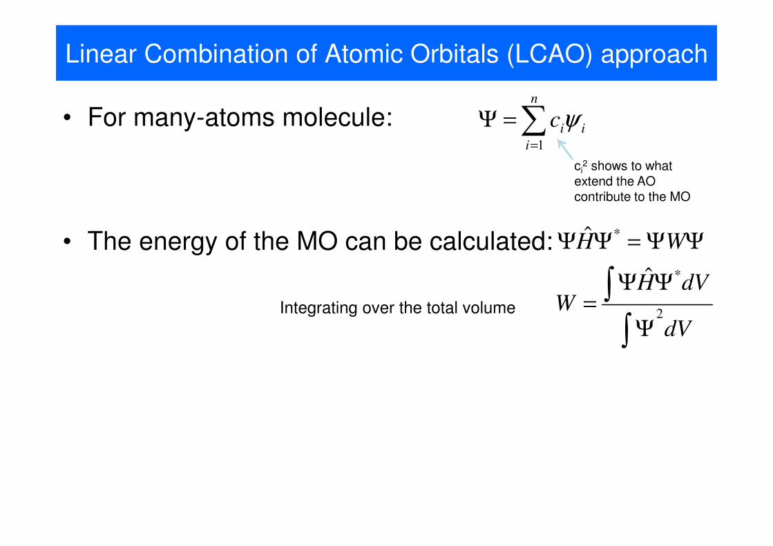
Linear Combination of Atomic Orbitals (LCAO) approach
• For many-atoms molecule: ∑=
=Ψn
i
iic1
ψ
ci2 shows to what
extend the AO contribute to the MO
• The energy of the MO can be calculated:
dV
dVHW
WH
2
*
*
ˆ
ˆ
∫
∫Ψ
ΨΨ=
ΨΨ=ΨΨ
Integrating over the total volume
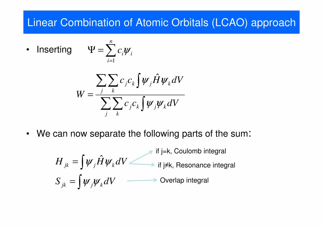
Linear Combination of Atomic Orbitals (LCAO) approach
• Inserting ∑=
=Ψn
i
iic1
ψ
• We can now separate the following parts of the sum:
dVcc
dVHcc
W
kj
j k
kj
kj
j k
kj
∫∑∑
∫∑∑=
ψψ
ψψ ˆ
dVS
dVHH
kjjk
kjjk
∫
∫=
=
ψψ
ψψ ˆ
Overlap integral
if j=k, Coulomb integral
if j≠k, Resonance integral
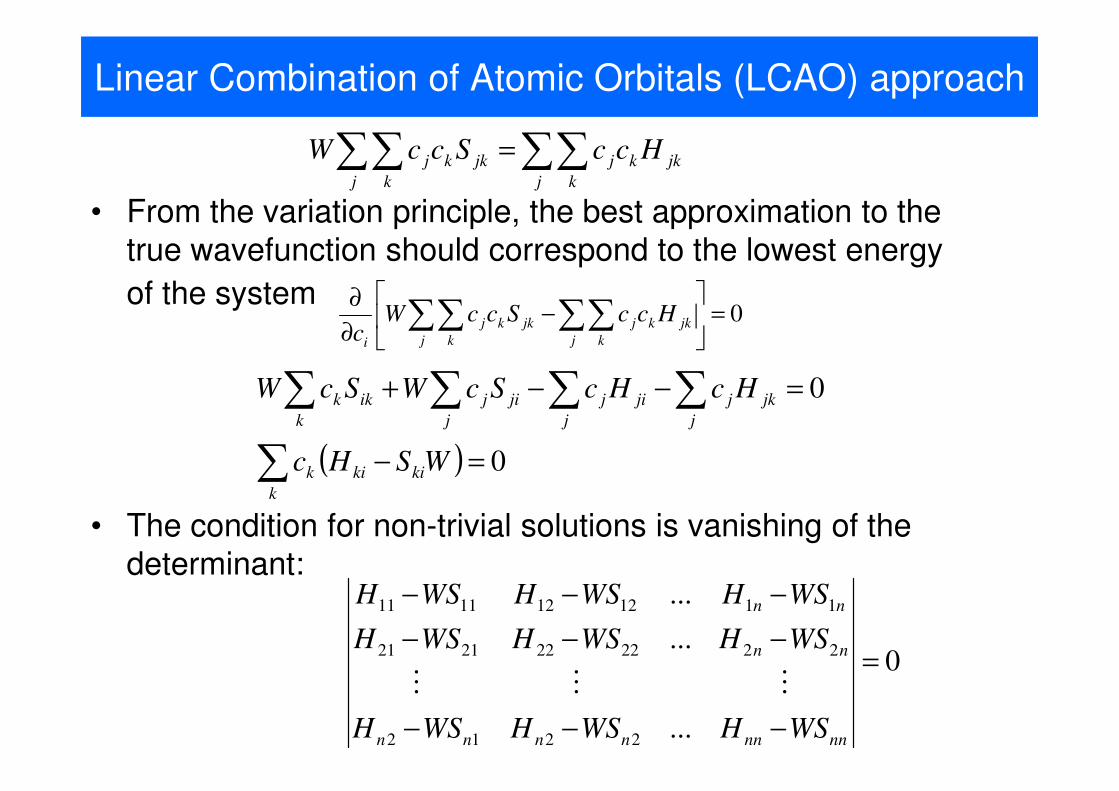
Linear Combination of Atomic Orbitals (LCAO) approach
• From the variation principle, the best approximation to the
true wavefunction should correspond to the lowest energy
of the system
• The condition for non-trivial solutions is vanishing of the
determinant:
jk
j k
kjjk
j k
kj HccSccW ∑∑∑∑ =
0=
−
∂
∂∑∑∑∑ jk
j k
kjjk
j k
kj
i
HccSccWc
( ) 0
0
=−
=−−+
∑
∑∑∑∑
WSHc
HcHcScWScW
kiki
k
k
jk
j
jji
j
jji
j
jik
k
k
0
...
...
...
2212
2222222121
1112121111
=
−−−
−−−
−−−
nnnnnnnn
nn
nn
WSHWSHWSH
WSHWSHWSH
WSHWSHWSH
���
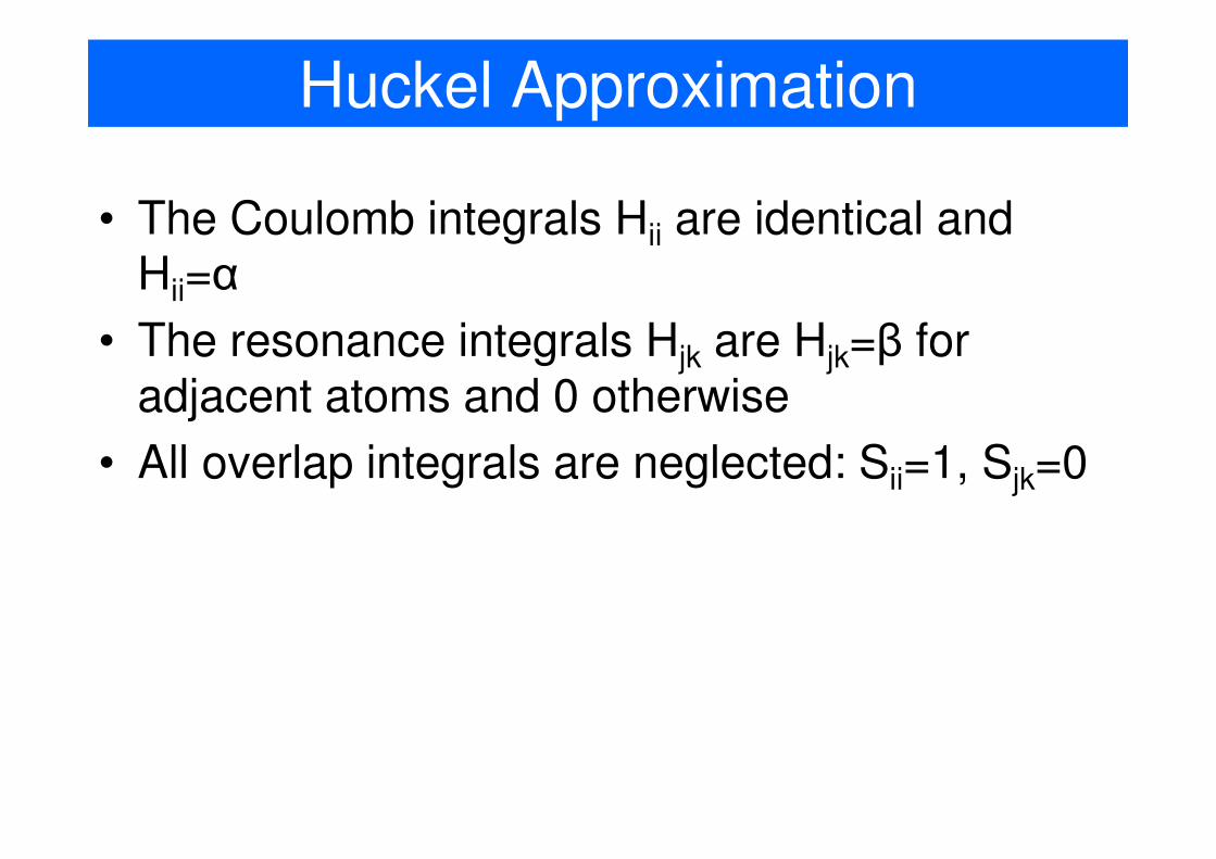
Huckel Approximation
• The Coulomb integrals Hii are identical and Hii=α
• The resonance integrals Hjk are Hjk=β for adjacent atoms and 0 otherwise
• All overlap integrals are neglected: Sii=1, Sjk=0
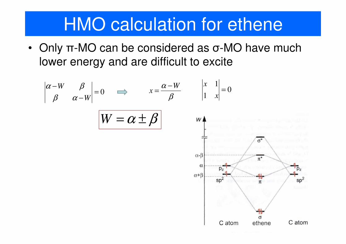
HMO calculation for ethene• Only π-MO can be considered as σ-MO have much
lower energy and are difficult to excite
0=−
−
W
W
αβ
βα
β
α Wx
−= 0
1
1=
x
x
βα ±=W
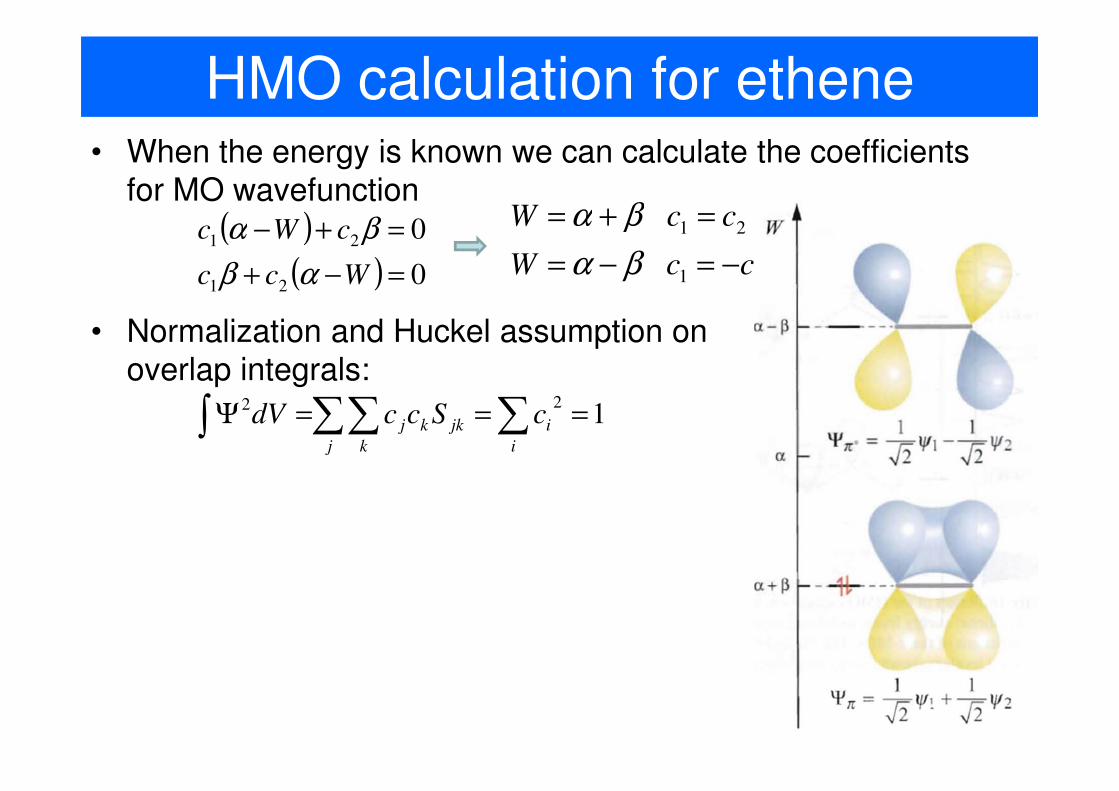
HMO calculation for ethene• When the energy is known we can calculate the coefficients
for MO wavefunction( )
( ) 0
0
21
21
=−+
=+−
Wcc
cWc
αβ
βα
21
21
ccW
ccW
−=−=
=+=
βα
βα
• Normalization and Huckel assumption on
overlap integrals:
∑∑∑∫ ===Ψi
ijk
j k
kj cSccdV 122
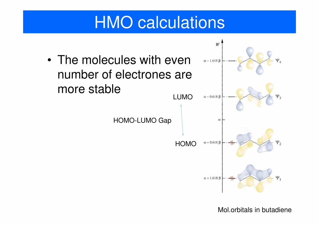
HMO calculations
• The molecules with even number of electrones are more stable
Mol.orbitals in butadiene
HOMO
LUMO
HOMO-LUMO Gap
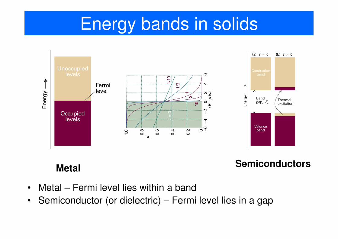
Energy bands in solids
• Metal – Fermi level lies within a band
• Semiconductor (or dielectric) – Fermi level lies in a gap
Metal Semiconductors
Intermediate case: molecules
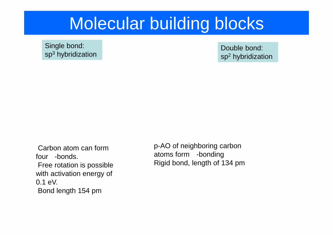
Molecular building blocks
• Carbon atom can form
four σ-bonds.
• Free rotation is possible
with activation energy of
0.1 eV.
• Bond length 154 pm
Double bond:
sp2 hybridization
p-AO of neighboring carbon
atoms form π-bonding
Rigid bond, length of 134 pm
Single bond:
sp3 hybridization
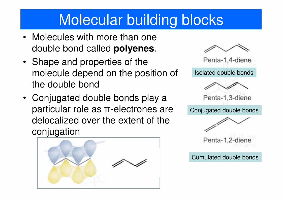
Molecular building blocks• Molecules with more than one
double bond called polyenes.
• Shape and properties of the
molecule depend on the position of
the double bond
• Conjugated double bonds play a
particular role as π-electrones are
delocalized over the extent of the
conjugation
Isolated double bonds
Conjugated double bonds
Cumulated double bonds
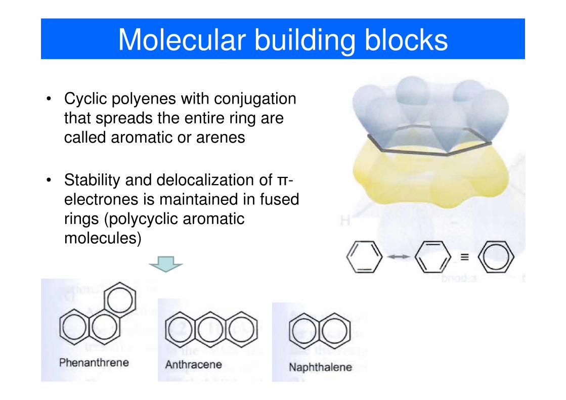
Molecular building blocks
• Cyclic polyenes with conjugation
that spreads the entire ring are
called aromatic or arenes
• Stability and delocalization of π-
electrones is maintained in fused
rings (polycyclic aromatic
molecules)
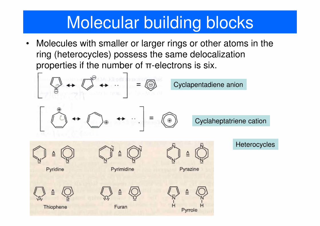
Molecular building blocks• Molecules with smaller or larger rings or other atoms in the
ring (heterocycles) possess the same delocalization
properties if the number of π-electrons is six.
Cyclapentadiene anion
Cyclaheptatriene cation
Heterocycles
Molecular building blocks
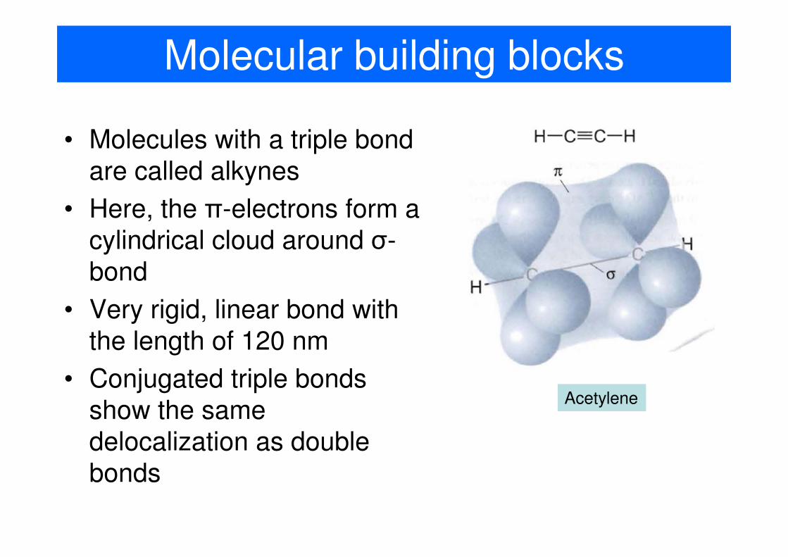
• Molecules with a triple bond
are called alkynes
• Here, the π-electrons form a
cylindrical cloud around σ-
bond
• Very rigid, linear bond with
the length of 120 nm
• Conjugated triple bonds
show the same
delocalization as double
bonds
Acetylene
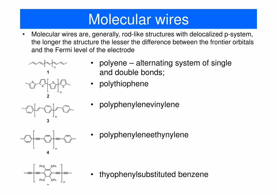
Molecular wires
• polyene – alternating system of single
and double bonds;
• polythiophene
• polyphenylenevinylene
• polyphenyleneethynylene
• thyophenylsubstituted benzene
• Molecular wires are, generally, rod-like structures with delocalized p-system, the longer the structure the lesser the difference between the frontier orbitals and the Fermi level of the electrode
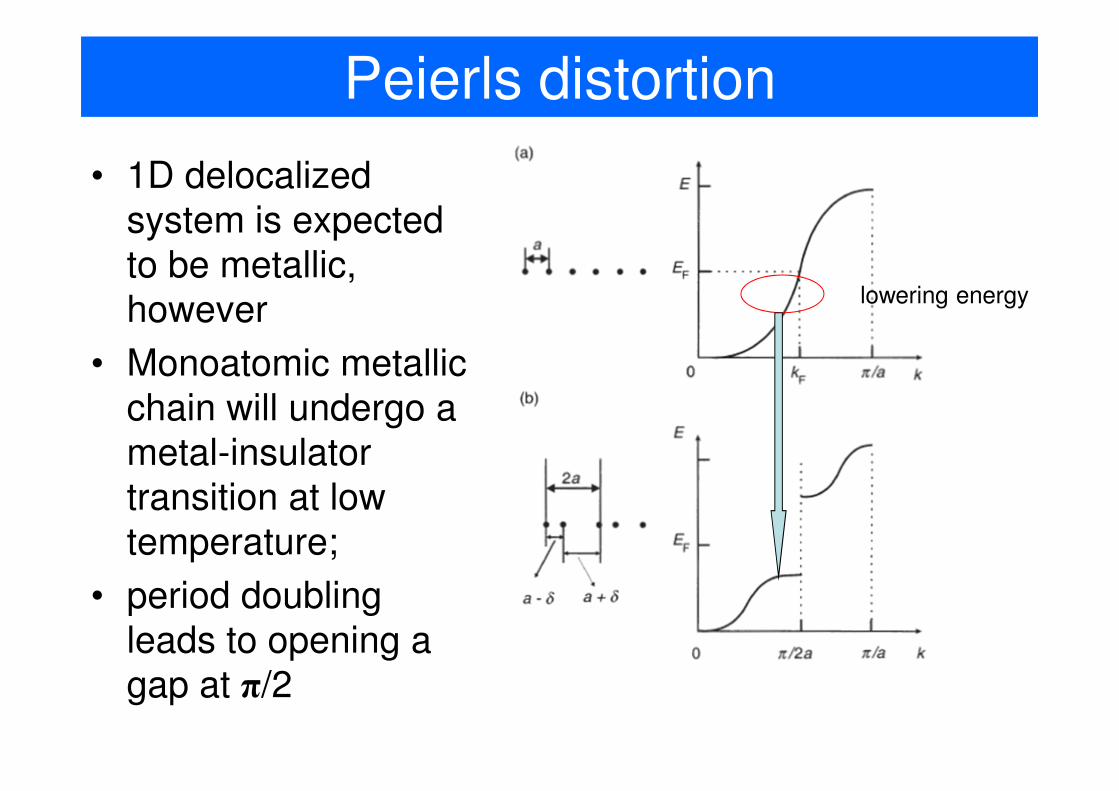
Peierls distortion
• 1D delocalized
system is expected
to be metallic,
however
• Monoatomic metallic
chain will undergo a
metal-insulator
transition at low
temperature;
• period doubling
leads to opening a gap at π/2
lowering energy
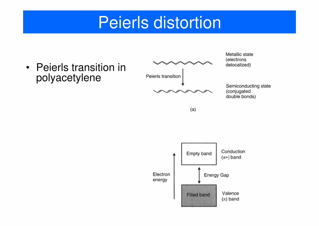
Peierls distortion
• Peierls transition in polyacetylene
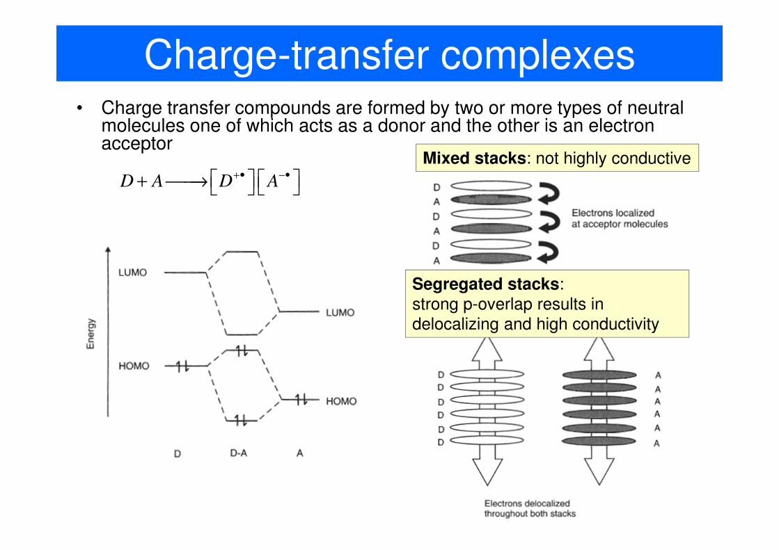
Charge-transfer complexes• Charge transfer compounds are formed by two or more types of neutral
molecules one of which acts as a donor and the other is an electron acceptor
D A D A+• −• + →
Mixed stacks: not highly conductive
Segregated stacks:
strong p-overlap results in
delocalizing and high conductivity
Charge-transfer complexes
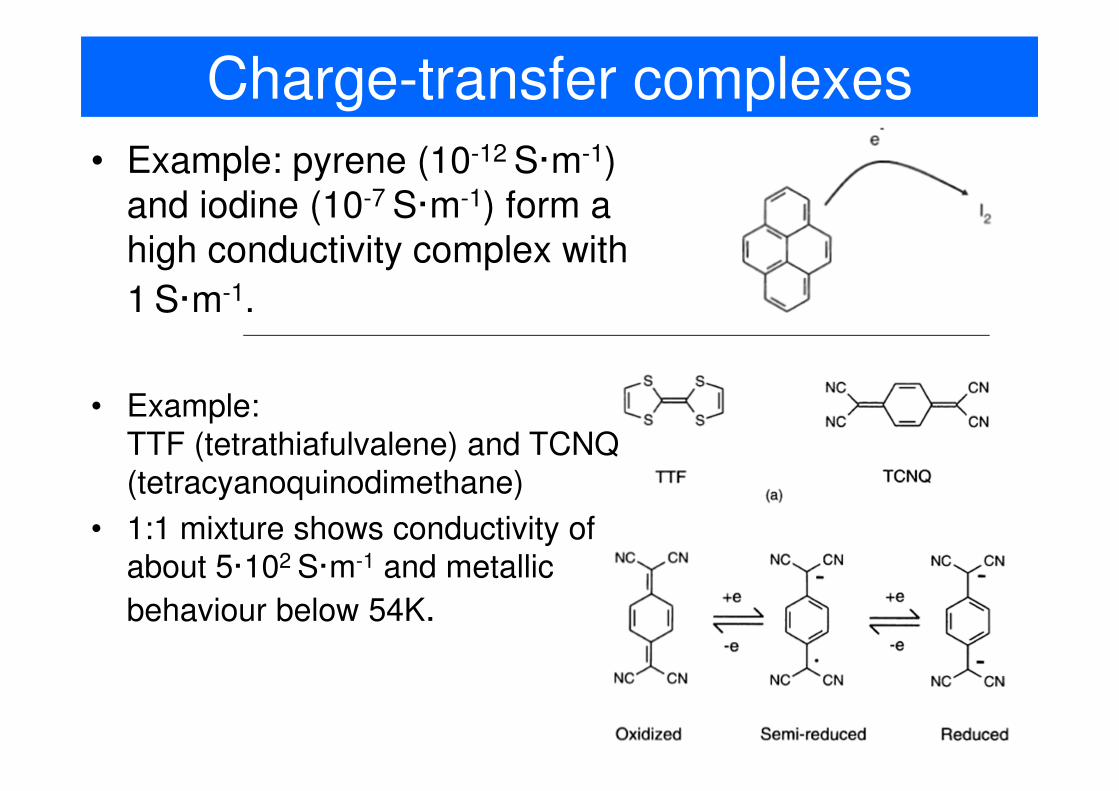
• Example: pyrene (10-12 S·m-1)
and iodine (10-7 S·m-1) form a
high conductivity complex with
1 S·m-1.
• Example:
TTF (tetrathiafulvalene) and TCNQ
(tetracyanoquinodimethane)
• 1:1 mixture shows conductivity of
about 5·102 S·m-1 and metallic
behaviour below 54K.
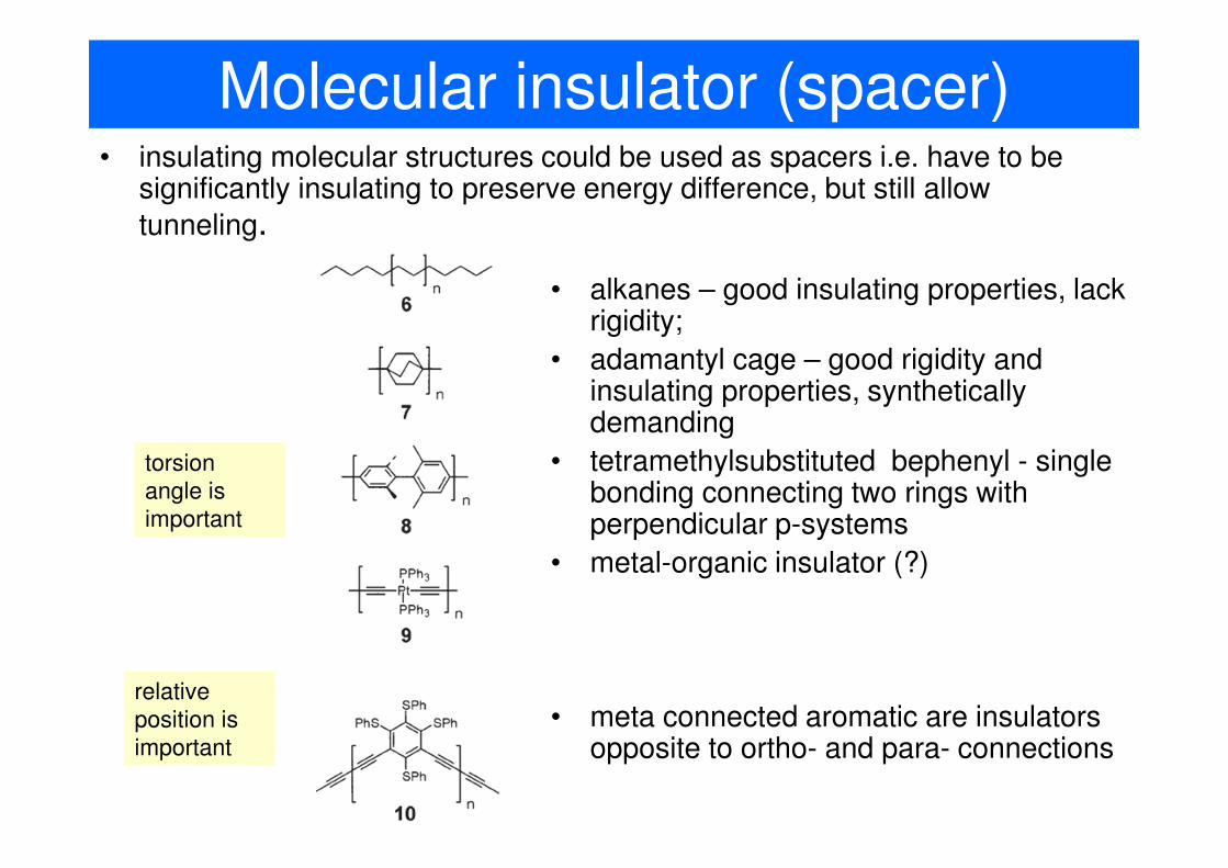
Molecular insulator (spacer)• insulating molecular structures could be used as spacers i.e. have to be
significantly insulating to preserve energy difference, but still allow
tunneling.
• alkanes – good insulating properties, lack rigidity;
• adamantyl cage – good rigidity and insulating properties, synthetically demanding
• tetramethylsubstituted bephenyl - single bonding connecting two rings with perpendicular p-systems
• metal-organic insulator (?)
• meta connected aromatic are insulators opposite to ortho- and para- connections
relative
position is
important
torsion
angle is
important
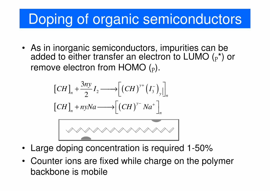
Doping of organic semiconductors
• As in inorganic semiconductors, impurities can be added to either transfer an electron to LUMO (p*) or
remove electron from HOMO (p).
[ ] ( ) ( )
[ ] ( )
2 3
3
2
y
n y n
y
nn
nyCH I CH I
CH nyNa CH Na
+ −
− +
+ →
+ →
• Large doping concentration is required 1-50%
• Counter ions are fixed while charge on the polymer
backbone is mobile
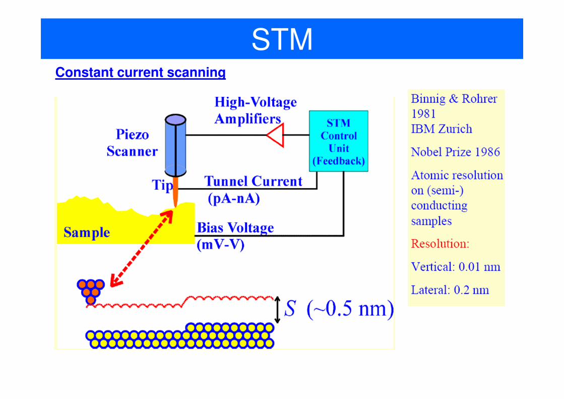
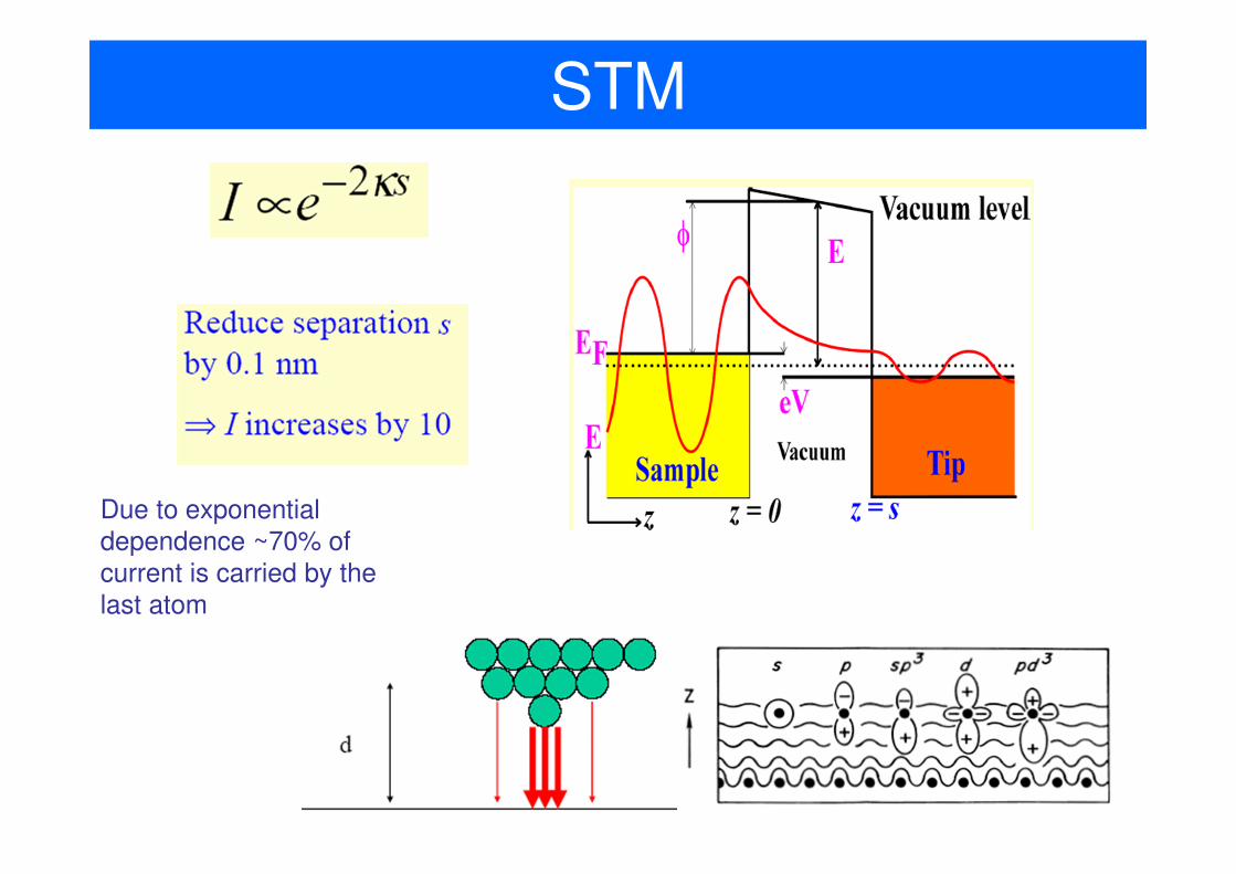
STMConstant current scanning
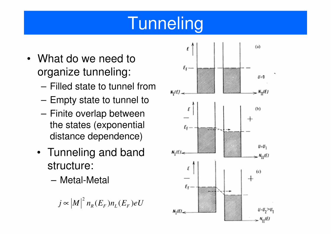
Tunneling
• What do we need to
organize tunneling:
– Filled state to tunnel from
– Empty state to tunnel to
– Finite overlap between
the states (exponential
distance dependence)
• Tunneling and band
structure:
– Metal-Metal
2( ) ( )R F L Fj M n E n E eU∝
STM
Due to exponential
dependence ~70% of
current is carried by the
last atom
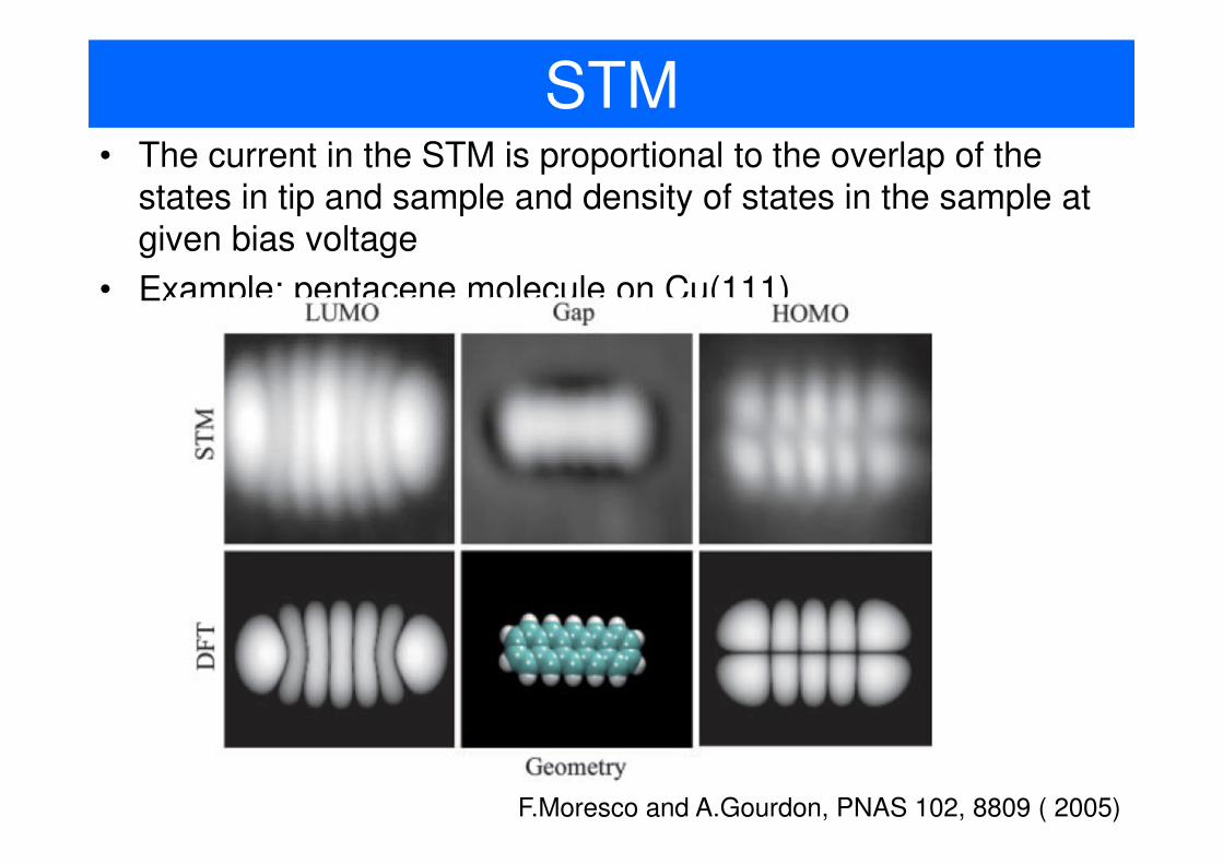
STM• The current in the STM is proportional to the overlap of the
states in tip and sample and density of states in the sample at
given bias voltage
• Example: pentacene molecule on Cu(111)
F.Moresco and A.Gourdon, PNAS 102, 8809 ( 2005)
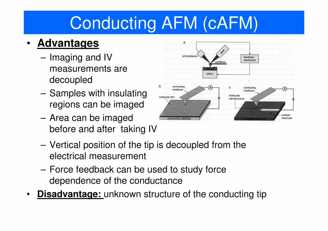
Conducting AFM (cAFM)• Advantages
– Imaging and IV
measurements are
decoupled
– Samples with insulating
regions can be imaged
– Area can be imaged
before and after taking IV
– Vertical position of the tip is decoupled from the
electrical measurement
– Force feedback can be used to study force
dependence of the conductance
• Disadvantage: unknown structure of the conducting tip
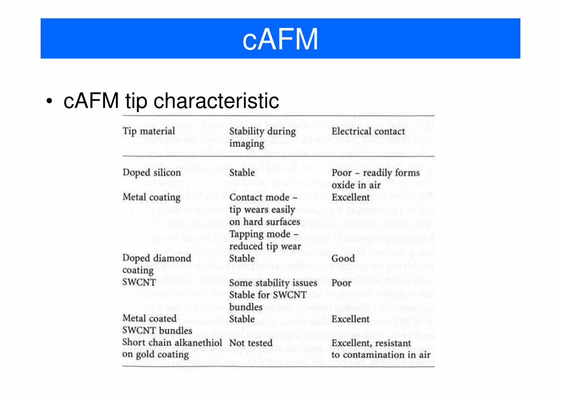
cAFM
• cAFM tip characteristic


![PP - Introduction · Particle Physics - Introduction A.A. 2017 - 2018 Paolo Bagnaia last mod. 26-Feb-18 . ... [Perkins] D.Perkins - Introduction to High Energy Physics, 4th ed.](https://static.fdocument.org/doc/165x107/5b4f64637f8b9a5a6f8c5607/pp-particle-physics-introduction-aa-2017-2018-paolo-bagnaia-last-mod.jpg)