INAx126 MicroPower Instrumentation Amplifier Single and ...
35
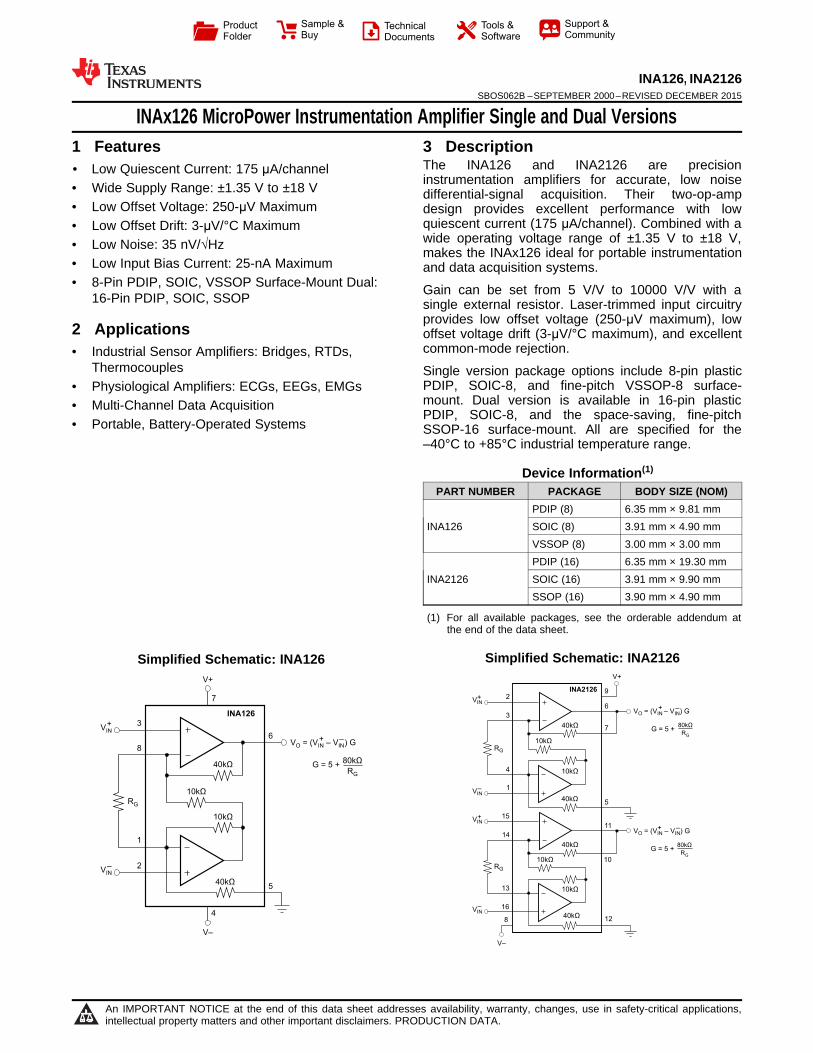
40kΩ 10kΩ 10kΩ 40kΩ INA2126 5 7 8 1 4 3 2 9 6 R G V IN – V IN + V+ V– V O = (V IN –V IN ) G – + G = 5 + V O = (V IN –V IN ) G – + G = 5 + 40kΩ 10kΩ 10kΩ 40kΩ 12 16 13 14 15 11 10 R G V IN – V IN + 80kΩ R G 80kΩ R G 40kΩ 10kΩ 10kΩ 40kΩ INA126 5 4 2 1 8 3 7 6 R G V IN – V IN + V+ V– V O = (V IN –V IN ) G – + 80kΩ R G G=5+ Product Folder Sample & Buy Technical Documents Tools & Software Support & Community INA126, INA2126 SBOS062B – SEPTEMBER 2000 – REVISED DECEMBER 2015 INAx126 MicroPower Instrumentation Amplifier Single and Dual Versions 1 Features 3 Description The INA126 and INA2126 are precision 1• Low Quiescent Current: 175 μA/channel instrumentation amplifiers for accurate, low noise • Wide Supply Range: ±1.35 V to ±18 V differential-signal acquisition. Their two-op-amp • Low Offset Voltage: 250-μV Maximum design provides excellent performance with low quiescent current (175 μA/channel). Combined with a • Low Offset Drift: 3-μV/°C Maximum wide operating voltage range of ±1.35 V to ±18 V, • Low Noise: 35 nV/√Hz makes the INAx126 ideal for portable instrumentation • Low Input Bias Current: 25-nA Maximum and data acquisition systems. • 8-Pin PDIP, SOIC, VSSOP Surface-Mount Dual: Gain can be set from 5 V/V to 10000 V/V with a 16-Pin PDIP, SOIC, SSOP single external resistor. Laser-trimmed input circuitry provides low offset voltage (250-μV maximum), low 2 Applications offset voltage drift (3-μV/°C maximum), and excellent common-mode rejection. • Industrial Sensor Amplifiers: Bridges, RTDs, Thermocouples Single version package options include 8-pin plastic PDIP, SOIC-8, and fine-pitch VSSOP-8 surface- • Physiological Amplifiers: ECGs, EEGs, EMGs mount. Dual version is available in 16-pin plastic • Multi-Channel Data Acquisition PDIP, SOIC-8, and the space-saving, fine-pitch • Portable, Battery-Operated Systems SSOP-16 surface-mount. All are specified for the –40°C to +85°C industrial temperature range. Device Information (1) PART NUMBER PACKAGE BODY SIZE (NOM) PDIP (8) 6.35 mm × 9.81 mm INA126 SOIC (8) 3.91 mm × 4.90 mm VSSOP (8) 3.00 mm × 3.00 mm PDIP (16) 6.35 mm × 19.30 mm INA2126 SOIC (16) 3.91 mm × 9.90 mm SSOP (16) 3.90 mm × 4.90 mm (1) For all available packages, see the orderable addendum at the end of the data sheet. Simplified Schematic: INA2126 Simplified Schematic: INA126 1 An IMPORTANT NOTICE at the end of this data sheet addresses availability, warranty, changes, use in safety-critical applications, intellectual property matters and other important disclaimers. PRODUCTION DATA.
Transcript of INAx126 MicroPower Instrumentation Amplifier Single and ...
40kΩ
10kΩ
10kΩ
40kΩ
INA2126
5
7
8
1
4
3
29
6
RG
VIN–
VIN+
V+
V–
VO = (VIN – VIN) G–+
G = 5 +
VO = (VIN – VIN) G–+
G = 5 +40kΩ
10kΩ
10kΩ
40kΩ 12
16
13
14
15
11
10RG
VIN–
VIN+
80kΩ
RG
80kΩ
RG
40kΩ
10kΩ
10kΩ
40kΩ
INA126
5
4
2
1
8
3
7
6
RG
VIN–
VIN+
V+
V–
VO = (VIN – VIN) G–+
80kΩ
RG
G = 5 +
Product
Folder
Sample &Buy
Technical
Documents
Tools &
Software
Support &Community
INA126, INA2126SBOS062B –SEPTEMBER 2000–REVISED DECEMBER 2015
INAx126 MicroPower Instrumentation Amplifier Single and Dual Versions1 Features 3 Description
The INA126 and INA2126 are precision1• Low Quiescent Current: 175 μA/channel
instrumentation amplifiers for accurate, low noise• Wide Supply Range: ±1.35 V to ±18 V differential-signal acquisition. Their two-op-amp• Low Offset Voltage: 250-μV Maximum design provides excellent performance with low
quiescent current (175 μA/channel). Combined with a• Low Offset Drift: 3-μV/°C Maximumwide operating voltage range of ±1.35 V to ±18 V,• Low Noise: 35 nV/√Hz makes the INAx126 ideal for portable instrumentation
• Low Input Bias Current: 25-nA Maximum and data acquisition systems.• 8-Pin PDIP, SOIC, VSSOP Surface-Mount Dual: Gain can be set from 5 V/V to 10000 V/V with a16-Pin PDIP, SOIC, SSOP single external resistor. Laser-trimmed input circuitry
provides low offset voltage (250-μV maximum), low2 Applications offset voltage drift (3-μV/°C maximum), and excellentcommon-mode rejection.• Industrial Sensor Amplifiers: Bridges, RTDs,
Thermocouples Single version package options include 8-pin plasticPDIP, SOIC-8, and fine-pitch VSSOP-8 surface-• Physiological Amplifiers: ECGs, EEGs, EMGsmount. Dual version is available in 16-pin plastic• Multi-Channel Data AcquisitionPDIP, SOIC-8, and the space-saving, fine-pitch
• Portable, Battery-Operated Systems SSOP-16 surface-mount. All are specified for the–40°C to +85°C industrial temperature range.
Device Information(1)
PART NUMBER PACKAGE BODY SIZE (NOM)PDIP (8) 6.35 mm × 9.81 mm
INA126 SOIC (8) 3.91 mm × 4.90 mmVSSOP (8) 3.00 mm × 3.00 mmPDIP (16) 6.35 mm × 19.30 mm
INA2126 SOIC (16) 3.91 mm × 9.90 mmSSOP (16) 3.90 mm × 4.90 mm
(1) For all available packages, see the orderable addendum atthe end of the data sheet.
Simplified Schematic: INA2126Simplified Schematic: INA126
1
An IMPORTANT NOTICE at the end of this data sheet addresses availability, warranty, changes, use in safety-critical applications,intellectual property matters and other important disclaimers. PRODUCTION DATA.
INA126, INA2126SBOS062B –SEPTEMBER 2000–REVISED DECEMBER 2015 www.ti.com
Table of Contents7.4 Device Functional Modes........................................ 111 Features .................................................................. 1
8 Application and Implementation ........................ 122 Applications ........................................................... 18.1 Application Information............................................ 123 Description ............................................................. 18.2 Typical Application ................................................. 124 Revision History..................................................... 2
9 Power Supply Recommendations ...................... 165 Pin Configuration and Functions ......................... 39.1 Low Voltage Operation ........................................... 166 Specifications......................................................... 5
10 Layout................................................................... 176.1 Absolute Maximum Ratings ...................................... 510.1 Layout Guidelines ................................................. 176.2 ESD Ratings ............................................................ 510.2 Layout Example .................................................... 186.3 Recommended Operating Conditions....................... 5
11 Device and Documentation Support ................. 196.4 Thermal Information: INA126.................................... 511.1 Related Links ........................................................ 196.5 Thermal Information: INA2126.................................. 611.2 Community Resources.......................................... 196.6 Electrical Characteristics........................................... 611.3 Trademarks ........................................................... 196.7 Typical Characteristics .............................................. 811.4 Electrostatic Discharge Caution............................ 197 Detailed Description ............................................ 1111.5 Glossary ................................................................ 197.1 Overview ................................................................. 11
12 Mechanical, Packaging, and Orderable7.2 Functional Block Diagram ....................................... 11Information ........................................................... 197.3 Feature Description................................................. 11
4 Revision HistoryNOTE: Page numbers for previous revisions may differ from page numbers in the current version.
Changes from Revision A (August 2005) to Revision B Page
• Added ESD Ratings table, Feature Description section, Device Functional Modes, Application and Implementationsection, Power Supply Recommendations section, Layout section, Device and Documentation Support section, andMechanical, Packaging, and Orderable Information section .................................................................................................. 1
2 Submit Documentation Feedback Copyright © 2000–2015, Texas Instruments Incorporated
Product Folder Links: INA126 INA2126
RG
V–
IN
V+
IN
V–
RG
V+
VO
Ref
1
2
3
4
8
7
6
5
INA126, INA2126www.ti.com SBOS062B –SEPTEMBER 2000–REVISED DECEMBER 2015
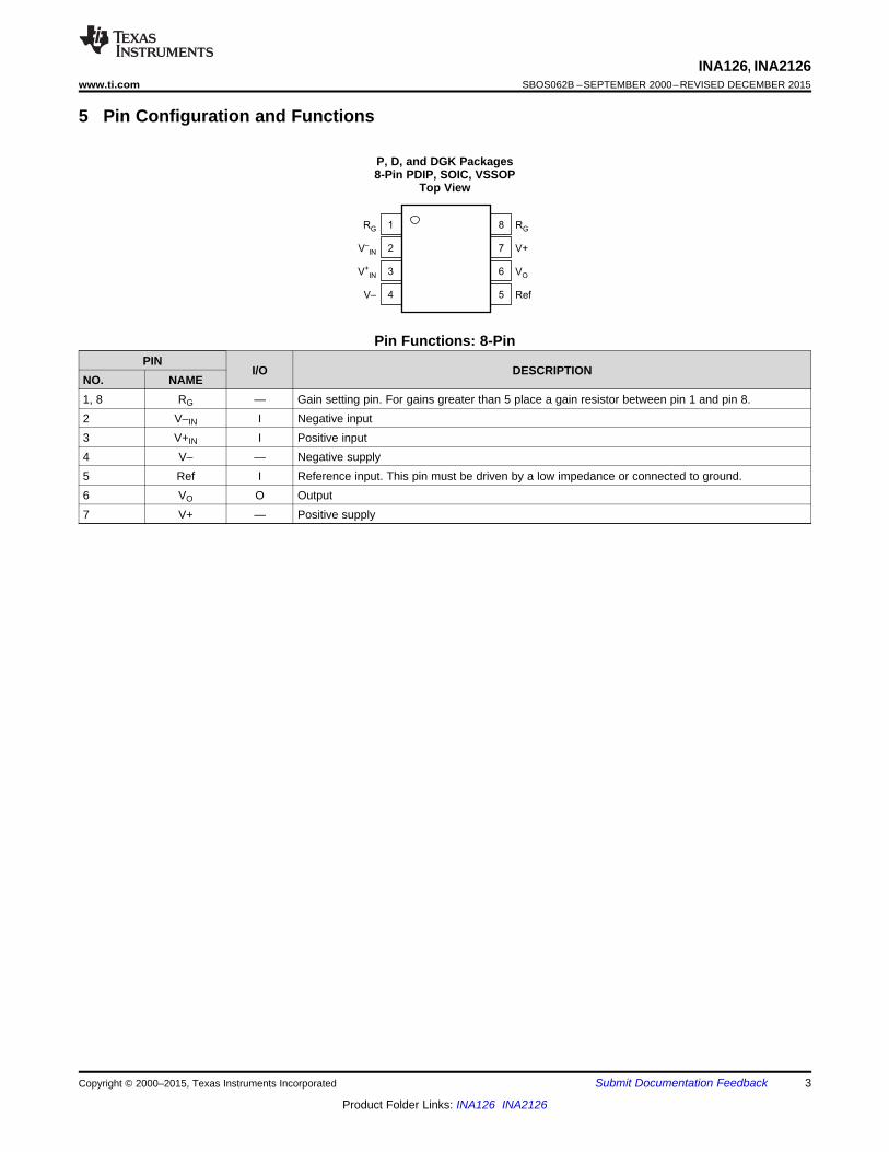
5 Pin Configuration and Functions
P, D, and DGK Packages8-Pin PDIP, SOIC, VSSOP
Top View
Pin Functions: 8-PinPIN
I/O DESCRIPTIONNO. NAME1, 8 RG — Gain setting pin. For gains greater than 5 place a gain resistor between pin 1 and pin 8.2 V–IN I Negative input3 V+IN I Positive input4 V– — Negative supply5 Ref I Reference input. This pin must be driven by a low impedance or connected to ground.6 VO O Output7 V+ — Positive supply
Copyright © 2000–2015, Texas Instruments Incorporated Submit Documentation Feedback 3
Product Folder Links: INA126 INA2126
VINA
VINA
RGA
RGA
VINB
VINB
RGB
RGB
1
2
3
4
RefA
VOA
SenseA
V–
5
6
7
8
16
15
14
13
RefB
VOB
SenseB
V+
12
11
10
9
–
+
–
+
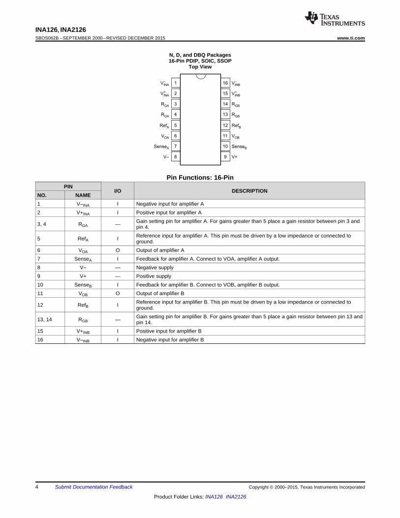
INA126, INA2126SBOS062B –SEPTEMBER 2000–REVISED DECEMBER 2015 www.ti.com
N, D, and DBQ Packages16-Pin PDIP, SOIC, SSOP
Top View
Pin Functions: 16-PinPIN
I/O DESCRIPTIONNO. NAME1 V–INA I Negative input for amplifier A2 V+INA I Positive input for amplifier A
Gain setting pin for amplifier A. For gains greater than 5 place a gain resistor between pin 3 and3, 4 RGA — pin 4.Reference input for amplifier A. This pin must be driven by a low impedance or connected to5 RefA I ground.
6 VOA O Output of amplifier A7 SenseA I Feedback for amplifier A. Connect to VOA, amplifier A output.8 V– — Negative supply9 V+ — Positive supply10 SenseB I Feedback for amplifier B. Connect to VOB, amplifier B output.11 VOB O Output of amplifier B
Reference input for amplifier B. This pin must be driven by a low impedance or connected to12 RefB I ground.Gain setting pin for amplifier B. For gains greater than 5 place a gain resistor between pin 13 and13, 14 RGB — pin 14.
15 V+INB I Positive input for amplifier B16 V–INB I Negative input for amplifier B
4 Submit Documentation Feedback Copyright © 2000–2015, Texas Instruments Incorporated
Product Folder Links: INA126 INA2126
INA126, INA2126www.ti.com SBOS062B –SEPTEMBER 2000–REVISED DECEMBER 2015
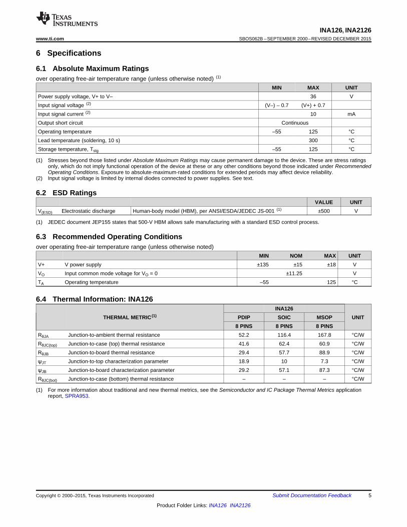
6 Specifications
6.1 Absolute Maximum Ratingsover operating free-air temperature range (unless otherwise noted) (1)
MIN MAX UNITPower supply voltage, V+ to V– 36 VInput signal voltage (2) (V–) – 0.7 (V+) + 0.7Input signal current (2) 10 mAOutput short circuit ContinuousOperating temperature –55 125 °CLead temperature (soldering, 10 s) 300 °CStorage temperature, Tstg –55 125 °C
(1) Stresses beyond those listed under Absolute Maximum Ratings may cause permanent damage to the device. These are stress ratingsonly, which do not imply functional operation of the device at these or any other conditions beyond those indicated under RecommendedOperating Conditions. Exposure to absolute-maximum-rated conditions for extended periods may affect device reliability.
(2) Input signal voltage is limited by internal diodes connected to power supplies. See text.
6.2 ESD RatingsVALUE UNIT
V(ESD) Electrostatic discharge Human-body model (HBM), per ANSI/ESDA/JEDEC JS-001 (1) ±500 V
(1) JEDEC document JEP155 states that 500-V HBM allows safe manufacturing with a standard ESD control process.
6.3 Recommended Operating Conditionsover operating free-air temperature range (unless otherwise noted)
MIN NOM MAX UNITV+ V power supply ±135 ±15 ±18 VVO Input common mode voltage for VO = 0 ±11.25 VTA Operating temperature –55 125 °C
6.4 Thermal Information: INA126INA126
THERMAL METRIC (1) PDIP SOIC MSOP UNIT8 PINS 8 PINS 8 PINS
RθJA Junction-to-ambient thermal resistance 52.2 116.4 167.8 °C/WRθJC(top) Junction-to-case (top) thermal resistance 41.6 62.4 60.9 °C/WRθJB Junction-to-board thermal resistance 29.4 57.7 88.9 °C/WψJT Junction-to-top characterization parameter 18.9 10 7.3 °C/WψJB Junction-to-board characterization parameter 29.2 57.1 87.3 °C/WRθJC(bot) Junction-to-case (bottom) thermal resistance – – – °C/W
(1) For more information about traditional and new thermal metrics, see the Semiconductor and IC Package Thermal Metrics applicationreport, SPRA953.
Copyright © 2000–2015, Texas Instruments Incorporated Submit Documentation Feedback 5
Product Folder Links: INA126 INA2126
INA126, INA2126SBOS062B –SEPTEMBER 2000–REVISED DECEMBER 2015 www.ti.com
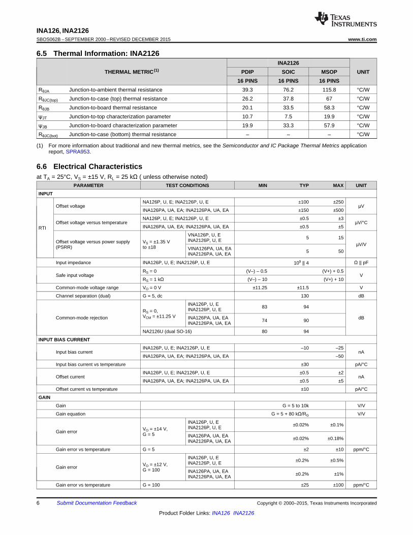
6.5 Thermal Information: INA2126INA2126
THERMAL METRIC (1) PDIP SOIC MSOP UNIT16 PINS 16 PINS 16 PINS
RθJA Junction-to-ambient thermal resistance 39.3 76.2 115.8 °C/WRθJC(top) Junction-to-case (top) thermal resistance 26.2 37.8 67 °C/WRθJB Junction-to-board thermal resistance 20.1 33.5 58.3 °C/WψJT Junction-to-top characterization parameter 10.7 7.5 19.9 °C/WψJB Junction-to-board characterization parameter 19.9 33.3 57.9 °C/WRθJC(bot) Junction-to-case (bottom) thermal resistance – – – °C/W
(1) For more information about traditional and new thermal metrics, see the Semiconductor and IC Package Thermal Metrics applicationreport, SPRA953.
6.6 Electrical Characteristicsat TA = 25°C, VS = ±15 V, RL = 25 kΩ ( unless otherwise noted)
PARAMETER TEST CONDITIONS MIN TYP MAX UNIT
INPUT
NA126P, U, E; INA2126P, U, E ±100 ±250Offset voltage µV
INA126PA, UA, EA; INA2126PA, UA, EA ±150 ±500
NA126P, U, E; INA2126P, U, E ±0.5 ±3Offset voltage versus temperature µV/°C
INA126PA, UA, EA; INA2126PA, UA, EA ±0.5 ±5RTIVNA126P, U, E 5 15INA2126P, U, EOffset voltage versus power supply VS = ±1.35 V µV/V(PSRR) to ±18 VINA126PA, UA, EA 5 50INA2126PA, UA, EA
Input impedance INA126P, U, E; INA2126P, U, E Ω || pF109 || 4
RS = 0 (V–) – 0.5 (V+) + 0.5Safe input voltage V
RS = 1 kΩ (V–) – 10 (V+) + 10
Common-mode voltage range VO = 0 V ±11.25 ±11.5 V
Channel separation (dual) G = 5, dc 130 dB
INA126P, U, E 83 94INA2126P, U, ERS = 0,VCM = ±11.25 VCommon-mode rejection INA126PA, UA, EA dB74 90INA2126PA, UA, EA
NA2126U (dual SO-16) 80 94
INPUT BIAS CURRENT
INA126P, U, E; INA2126P, U, E –10 –25Input bias current nA
INA126PA, UA, EA; INA2126PA, UA, EA –50
Input bias current vs temperature ±30 pA/°C
INA126P, U, E; INA2126P, U, E ±0.5 ±2Offset current nA
INA126PA, UA, EA; INA2126PA, UA, EA ±0.5 ±5
Offset current vs temperature ±10 pA/°C
GAIN
Gain G = 5 to 10k V/V
Gain equation G = 5 + 80 kΩ/RG V/V
INA126P, U, E ±0.02% ±0.1%INA2126P, U, EVO = ±14 V,Gain error G = 5 INA126PA, UA, EA ±0.02% ±0.18%INA2126PA, UA, EA
Gain error vs temperature G = 5 ±2 ±10 ppm/°C
INA126P, U, E ±0.2% ±0.5%INA2126P, U, EVO = ±12 V,Gain error G = 100 INA126PA, UA, EA ±0.2% ±1%INA2126PA, UA, EA
Gain error vs temperature G = 100 ±25 ±100 ppm/°C
6 Submit Documentation Feedback Copyright © 2000–2015, Texas Instruments Incorporated
Product Folder Links: INA126 INA2126
INA126, INA2126www.ti.com SBOS062B –SEPTEMBER 2000–REVISED DECEMBER 2015
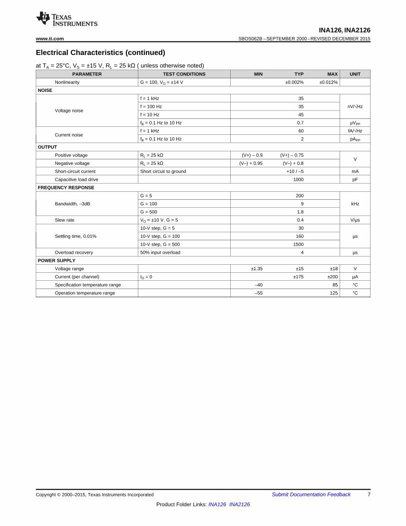
Electrical Characteristics (continued)at TA = 25°C, VS = ±15 V, RL = 25 kΩ ( unless otherwise noted)
PARAMETER TEST CONDITIONS MIN TYP MAX UNIT
Nonlinearity G = 100, VO = ±14 V ±0.002% ±0.012%
NOISE
f = 1 kHz 35
f = 100 Hz 35 nV/√HzVoltage noise
f = 10 Hz 45
fB = 0.1 Hz to 10 Hz 0.7 μVPP
f = 1 kHz 60 fA/√HzCurrent noise
fB = 0.1 Hz to 10 Hz 2 pAPP
OUTPUT
Positive voltage RL = 25 kΩ (V+) – 0.9 (V+) – 0.75V
Negative voltage RL = 25 kΩ (V–) + 0.95 (V–) + 0.8
Short-circuit current Short circuit to ground +10 / –5 mA
Capacitive load drive 1000 pF
FREQUENCY RESPONSE
G = 5 200
Bandwidth, –3dB G = 100 9 kHz
G = 500 1.8
Slew rate VO = ±10 V, G = 5 0.4 V/μs
10-V step, G = 5 30
Settling time, 0.01% 10-V step, G = 100 160 µs
10-V step, G = 500 1500
Overload recovery 50% input overload 4 µs
POWER SUPPLY
Voltage range ±1.35 ±15 ±18 V
Current (per channel) IO = 0 ±175 ±200 µA
Specification temperature range –40 85 °C
Operation temperature range –55 125 °C
Copyright © 2000–2015, Texas Instruments Incorporated Submit Documentation Feedback 7
Product Folder Links: INA126 INA2126
Output Voltage (V)
Com
mon-M
ode V
oltage (
V)
–15 –10 0 5 15–5
15
10
5
0
–5
–10
–15
10
VD/2
+
+–
–
VCM
VOVD/2 Ref
–15V
+15V
+
Limited by A2 output swing—see text
Limited by A2 output swing—see text
Output Voltage (V)
Inp
ut C
om
mon
-Mo
de V
oltag
e (
V)
–5 –4 5–3 –2 –1 0 1 2 3 4
5
4
3
2
1
0
–1
–2
–3
–4
–5
Limited by A2 output swing—see text
Limited by A2 output swing—see text
VS = ±5VVS = +5V/0V
VREF = 2.5V
120
100
80
60
40
20
0
Pow
er
Supply
Reje
ction (
dB
)
Frequency (Hz)
10 100 1k 10k 100k 1M
G = 1000
G = 100
G = 5
120
100
80
60
40
20
0
Po
we
r S
up
ply
Re
jectio
n (
dB
)
Frequency (Hz)
10 100 1k 10k 100k 1M
G = 1000
G = 100
G = 5
70
60
50
40
30
20
10
0
–10
Ga
in (
dB
)
Frequency (Hz)
100 1k 10k 100k 1M
G = 1000
G = 100
G = 20
G = 5
110
100
90
80
70
60
50
40
30
20
10
0
Co
mm
on
-Mo
de
Re
jectio
n (
dB
)
Frequency (Hz)
10 100 1k 10k 100k 1M
G = 1000
G = 100
G = 5
INA126, INA2126SBOS062B –SEPTEMBER 2000–REVISED DECEMBER 2015 www.ti.com
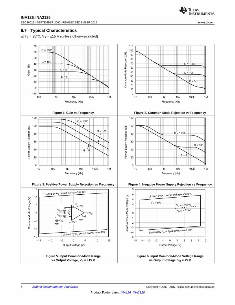
6.7 Typical Characteristicsat TA = 25°C, VS = ±15 V (unless otherwise noted)
Figure 1. Gain vs Frequency Figure 2. Common-Mode Rejection vs Frequency
Figure 3. Positive Power Supply Rejection vs Frequency Figure 4. Negative Power Supply Rejection vs Frequency
Figure 5. Input Common-Mode Range Figure 6. Input Common-Mode Voltage Rangevs Output Voltage, VS = ±15 V vs Output Voltage, VS = ±5 V
8 Submit Documentation Feedback Copyright © 2000–2015, Texas Instruments Incorporated
Product Folder Links: INA126 INA2126
Frequency (Hz)
TH
D+
N(%
)
10 100 1k
1
0.1
0.01
0.001
10k
RL = 100kΩ
G = 5
RL = 10kΩ
0 1 2 3 4 5
Output Current (mA)
Ou
tpu
t V
olta
ge (
V)
Sourcing Current
Sinking Current
V+
(V+)–1
(V+)–2
(V–)+2
(V–)+1
V–
Time After Turn-On (ms)
Offse
t V
olta
ge C
han
ge (
µV
)
0 1 102 3 4 5 6 7 8 9
10
8
6
4
2
0
–2
–4
–6
–8
–10
(Noise)
Temperature (°C)
Qu
iesce
nt
Cu
rre
nt
(µA
)
Sle
w R
ate
(V
/µs)
300
250
200
150
100
50
0
0.6
0.5
0.4
0.3
0.2
0.1
0
–75 –50 –25 0 25 50 75 100 125
+SR
–SR
VS = ±5V
VS = ±1.35VIQ
100
10
1
1k
100
10
Input V
oltage N
ois
e (
nV
/H
z)
√
Frequency (Hz)
1 10 100 10k1k
Input C
urr
ent N
ois
e (
fA/
Hz)
√
Voltage Noise
Current Noise
Gain (V/V)
Settlin
gT
ime (
µs)
1000
100
10
1 10 100 1k
0.01%
0.1%
INA126, INA2126www.ti.com SBOS062B –SEPTEMBER 2000–REVISED DECEMBER 2015
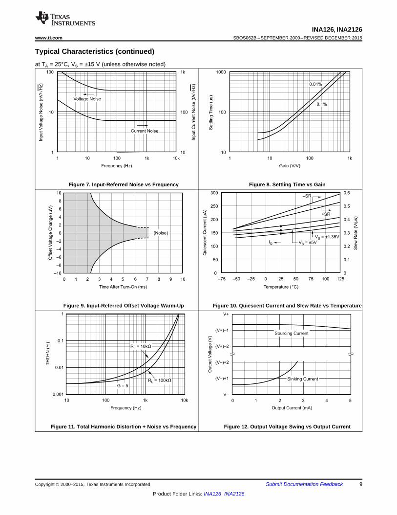
Typical Characteristics (continued)at TA = 25°C, VS = ±15 V (unless otherwise noted)
Figure 7. Input-Referred Noise vs Frequency Figure 8. Settling Time vs Gain
Figure 9. Input-Referred Offset Voltage Warm-Up Figure 10. Quiescent Current and Slew Rate vs Temperature
Figure 11. Total Harmonic Distortion + Noise vs Frequency Figure 12. Output Voltage Swing vs Output Current
Copyright © 2000–2015, Texas Instruments Incorporated Submit Documentation Feedback 9
Product Folder Links: INA126 INA2126
160
150
140
130
120
110
100
90
80
70
60
Se
pa
ratio
n (
dB
)
Frequency (Hz)
100 1k 10k 100k 1M
G = 1000
G = 100
G = 5
Measurement limited
by amplifier or
measurement noise.
RL = 25kΩ
5V
/div
50µs/div
0.2
V/d
iv
500ms/div
20m
V/d
iv
50µs/div
20m
V/d
iv
50µs/div
INA126, INA2126SBOS062B –SEPTEMBER 2000–REVISED DECEMBER 2015 www.ti.com
Typical Characteristics (continued)at TA = 25°C, VS = ±15 V (unless otherwise noted)
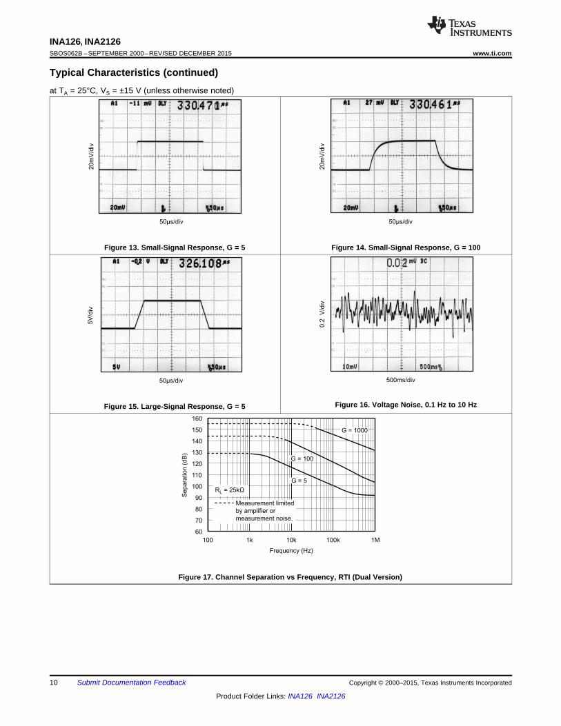
Figure 13. Small-Signal Response, G = 5 Figure 14. Small-Signal Response, G = 100
Figure 16. Voltage Noise, 0.1 Hz to 10 HzFigure 15. Large-Signal Response, G = 5
Figure 17. Channel Separation vs Frequency, RTI (Dual Version)
10 Submit Documentation Feedback Copyright © 2000–2015, Texas Instruments Incorporated
Product Folder Links: INA126 INA2126
+ +
REF
-IN
+IN
OUT
RG
INA126, INA2126www.ti.com SBOS062B –SEPTEMBER 2000–REVISED DECEMBER 2015
7 Detailed Description
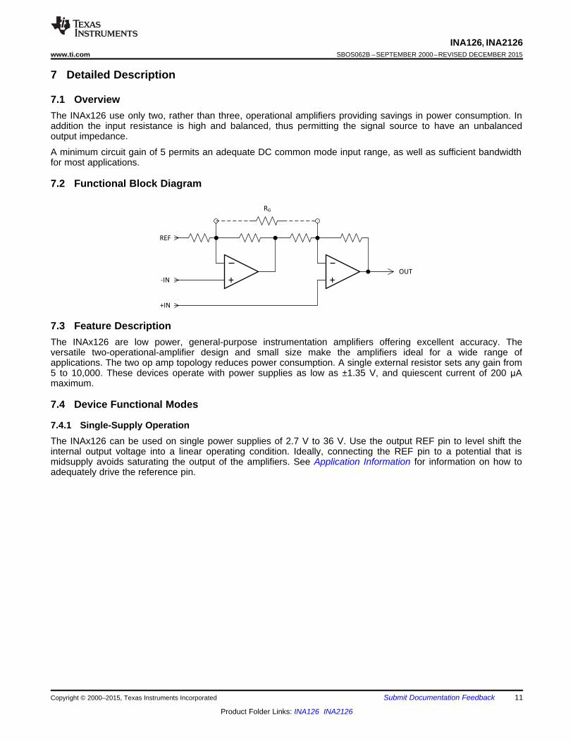
7.1 OverviewThe INAx126 use only two, rather than three, operational amplifiers providing savings in power consumption. Inaddition the input resistance is high and balanced, thus permitting the signal source to have an unbalancedoutput impedance.
A minimum circuit gain of 5 permits an adequate DC common mode input range, as well as sufficient bandwidthfor most applications.
7.2 Functional Block Diagram
7.3 Feature DescriptionThe INAx126 are low power, general-purpose instrumentation amplifiers offering excellent accuracy. Theversatile two-operational-amplifier design and small size make the amplifiers ideal for a wide range ofapplications. The two op amp topology reduces power consumption. A single external resistor sets any gain from5 to 10,000. These devices operate with power supplies as low as ±1.35 V, and quiescent current of 200 μAmaximum.
7.4 Device Functional Modes
7.4.1 Single-Supply OperationThe INAx126 can be used on single power supplies of 2.7 V to 36 V. Use the output REF pin to level shift theinternal output voltage into a linear operating condition. Ideally, connecting the REF pin to a potential that ismidsupply avoids saturating the output of the amplifiers. See Application Information for information on how toadequately drive the reference pin.
Copyright © 2000–2015, Texas Instruments Incorporated Submit Documentation Feedback 11
Product Folder Links: INA126 INA2126
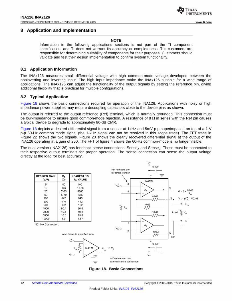
DESIRED GAIN RG NEAREST 1%
(V/V) (Ω) RG VALUE
5 NC NC
10 16k 15.8k
20 5333 5360
50 1779 1780
100 842 845
200 410 412
500 162 162
1000 80.4 80.6
2000 40.1 40.2
5000 16.0 15.8
10000 8.0 7.87
NC: No Connection.
40kΩ
10kΩ
10kΩ
40kΩ
INA126
5
4
2
1
8
3
7
6
RG
RG
VIN
A2
A1
–
VIN+
VIN–
VIN+
V+
V–
INA126
0.1µF
0.1µF
VO
VO
Ref
!
Ref
Load
+
–
Also drawn in simplified form:
VO = (VIN – VIN) G–+
G = 5 +
!
Pin numbers are
for single version
!Dual version has
external sense connection.
80kΩ
RG
INA126, INA2126SBOS062B –SEPTEMBER 2000–REVISED DECEMBER 2015 www.ti.com
8 Application and Implementation
NOTEInformation in the following applications sections is not part of the TI componentspecification, and TI does not warrant its accuracy or completeness. TI’s customers areresponsible for determining suitability of components for their purposes. Customers shouldvalidate and test their design implementation to confirm system functionality.
8.1 Application InformationThe INAx126 measures small differential voltage with high common-mode voltage developed between thenoninverting and inverting input. The high input impedance make the INAx126 suitable for a wide range ofapplications. The INAx126 can adjust the functionality of the output signals by setting the reference pin, givingadditional flexibility that is practical for multiple configurations.
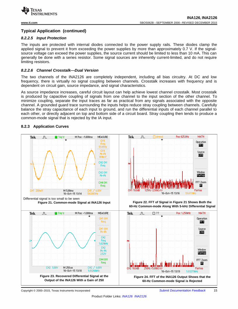
8.2 Typical ApplicationFigure 18 shows the basic connections required for operation of the INA126. Applications with noisy or highimpedance power supplies may require decoupling capacitors close to the device pins as shown.
The output is referred to the output reference (Ref) terminal, which is normally grounded. This connection mustbe low-impedance to ensure good common-mode rejection. A resistance of 8 Ω in series with the Ref pin causesa typical device to degrade to approximately 80-dB CMR.
Figure 18 depicts a desired differential signal from a sensor at 1kHz and 5mV p-p superimposed on top of a 1-Vp-p 60-Hz common mode signal (the 1-kHz signal can not be resolved in this scope trace). The FFT trace inFigure 22 shows the two signals. Figure 23 shows the clearly recovered differential signal at the output of theINA126 operating at a gain of 250. The FFT of figure 4 shows the 60-Hz common-mode is no longer visible.
The dual version (INA2126) has feedback-sense connections, SenseA and SenseB. These must be connected totheir respective output terminals for proper operation. The sense connection can sense the output voltagedirectly at the load for best accuracy.
Figure 18. Basic Connections
12 Submit Documentation Feedback Copyright © 2000–2015, Texas Instruments Incorporated
Product Folder Links: INA126 INA2126
10kΩOPA237
±10mV
Adjustment Range
100Ω
100Ω
100µA
1/2 REF200
100µA
1/2 REF200
V+
V–
RG INA126
Ref
VO!
VIN–
VIN+
! Dual version has
external sense connection.
INA126, INA2126www.ti.com SBOS062B –SEPTEMBER 2000–REVISED DECEMBER 2015
Typical Application (continued)8.2.1 Design RequirementsFor the traces shown in Figure 19 and Figure 20:• Common-mode rejection of at least 80dB• Gain of 250
8.2.2 Detailed Design Procedure
8.2.2.1 Setting the GainGain is set by connecting an external resistor, RG:
g = 5 + 80 kΩ/RG (1)
Commonly used gains and RG resistor values are shown in Figure 18.
The 80-kΩ term in Equation 1 comes from the internal metal film resistors, which are laser-trimmed to accurateabsolute values. The accuracy and temperature coefficient of these resistors are included in the gain accuracyand drift specifications.
The stability and temperature drift of the external gain setting resistor, RG, also affects gain. The RG contributionto gain accuracy and drift can be directly inferred from Equation 1. Low resistor values required for high gain canmake wiring resistance important. Sockets add to the wiring resistance, which contributes additional gain error ingains of approximately 100 or greater.
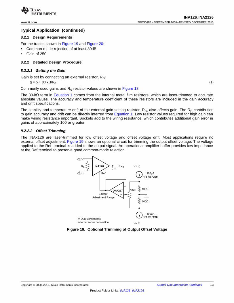
8.2.2.2 Offset TrimmingThe INAx126 are laser-trimmed for low offset voltage and offset voltage drift. Most applications require noexternal offset adjustment. Figure 19 shows an optional circuit for trimming the output offset voltage. The voltageapplied to the Ref terminal is added to the output signal. An operational amplifier buffer provides low impedanceat the Ref terminal to preserve good common-mode rejection.
Figure 19. Optional Trimming of Output Offset Voltage
Copyright © 2000–2015, Texas Instruments Incorporated Submit Documentation Feedback 13
Product Folder Links: INA126 INA2126
47kΩ47kΩ
10kΩ
Microphone,
Hydrophone
etc.
Thermocouple
Center-tap provides
bias current return.
INA126
INA126
INA126
INA126, INA2126SBOS062B –SEPTEMBER 2000–REVISED DECEMBER 2015 www.ti.com
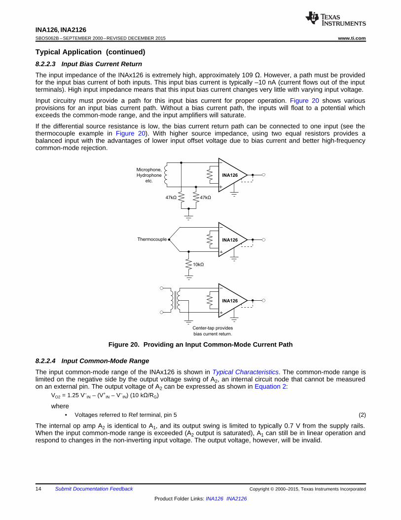
Typical Application (continued)8.2.2.3 Input Bias Current ReturnThe input impedance of the INAx126 is extremely high, approximately 109 Ω. However, a path must be providedfor the input bias current of both inputs. This input bias current is typically –10 nA (current flows out of the inputterminals). High input impedance means that this input bias current changes very little with varying input voltage.
Input circuitry must provide a path for this input bias current for proper operation. Figure 20 shows variousprovisions for an input bias current path. Without a bias current path, the inputs will float to a potential whichexceeds the common-mode range, and the input amplifiers will saturate.
If the differential source resistance is low, the bias current return path can be connected to one input (see thethermocouple example in Figure 20). With higher source impedance, using two equal resistors provides abalanced input with the advantages of lower input offset voltage due to bias current and better high-frequencycommon-mode rejection.
Figure 20. Providing an Input Common-Mode Current Path
8.2.2.4 Input Common-Mode RangeThe input common-mode range of the INAx126 is shown in Typical Characteristics. The common-mode range islimited on the negative side by the output voltage swing of A2, an internal circuit node that cannot be measuredon an external pin. The output voltage of A2 can be expressed as shown in Equation 2:
VO2 = 1.25 V–IN – (V+
IN – V–IN) (10 kΩ/RG)
where• Voltages referred to Ref terminal, pin 5 (2)
The internal op amp A2 is identical to A1, and its output swing is limited to typically 0.7 V from the supply rails.When the input common-mode range is exceeded (A2 output is saturated), A1 can still be in linear operation andrespond to changes in the non-inverting input voltage. The output voltage, however, will be invalid.
14 Submit Documentation Feedback Copyright © 2000–2015, Texas Instruments Incorporated
Product Folder Links: INA126 INA2126
INA126, INA2126www.ti.com SBOS062B –SEPTEMBER 2000–REVISED DECEMBER 2015
Typical Application (continued)8.2.2.5 Input ProtectionThe inputs are protected with internal diodes connected to the power supply rails. These diodes clamp theapplied signal to prevent it from exceeding the power supplies by more than approximately 0.7 V. If the signal-source voltage can exceed the power supplies, the source current should be limited to less than 10 mA. This cangenerally be done with a series resistor. Some signal sources are inherently current-limited, and do not requirelimiting resistors.
8.2.2.6 Channel Crosstalk—Dual VersionThe two channels of the INA2126 are completely independent, including all bias circuitry. At DC and lowfrequency, there is virtually no signal coupling between channels. Crosstalk increases with frequency and isdependent on circuit gain, source impedance, and signal characteristics.
As source impedance increases, careful circuit layout can help achieve lowest channel crosstalk. Most crosstalkis produced by capacitive coupling of signals from one channel to the input section of the other channel. Tominimize coupling, separate the input traces as far as practical from any signals associated with the oppositechannel. A grounded guard trace surrounding the inputs helps reduce stray coupling between channels. Carefullybalance the stray capacitance of each input to ground, and run the differential inputs of each channel parallel toeach other, or directly adjacent on top and bottom side of a circuit board. Stray coupling then tends to produce acommon-mode signal that is rejected by the IA input.
8.2.3 Application Curves
spaceDifferential signal is too small to be seenFigure 22. FFT of Signal in Figure 21 Shows Both theFigure 21. Common-mode Signal at INA126 Input
60-Hz Common-mode Along With 5-kHz Differential Signal
Figure 23. Recovered Differential Signal at the Figure 24. FFT of the INA126 Output Shows that theOutput of the INA126 With a Gain of 250 60-Hz Common-mode Signal is Rejected
Copyright © 2000–2015, Texas Instruments Incorporated Submit Documentation Feedback 15
Product Folder Links: INA126 INA2126
40kΩ
10kΩ
10kΩ
40kΩ
INA126
5 1.2V
4
4
6 8
2
1
8
3
7
6
RG
R1
1kΩ
C1
0.47µF
R2
1kΩ
+5V
R1, C1, R2:
340Hz LP
BridgeSensor
2.5V – ∆V
2.5V + ∆V
REF1004C-1.2
33µA
2
3
1
+IN
–IN
VREF
D
ADS7817
12-Bit
A/D
CS
Ck
6 Serial
Data
Chip
Select
INA126 and ADS7817
are available in fine-pitch
MSOP-8 package
!Dual version has external
sense connection. Pin numbers
shown are for single version.
Clock
5
7
4
8
A2
A1
The ADS7817’s VREF input current is proportional to conversion rate. A
conversion rate of 10kS/s or slower assures enough current to turn on the
reference diode. Converter input range is ±1.2V. Output swing limitation of
INA126 limits the A/D converter to somewhat greater than 11 bits of range.
A similar instrumentation amplifier, INA125, provides
an internal reference voltage for sensor excitation
and/or A/D converter reference.
!
INA126, INA2126SBOS062B –SEPTEMBER 2000–REVISED DECEMBER 2015 www.ti.com
9 Power Supply Recommendations
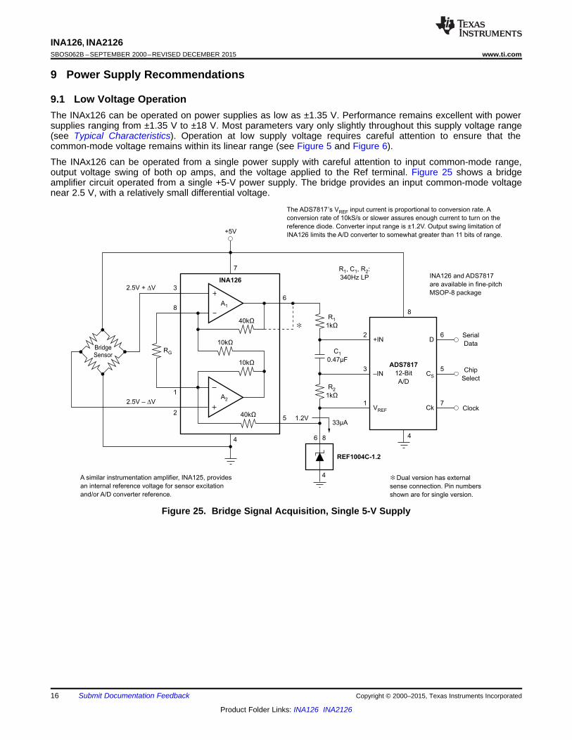
9.1 Low Voltage OperationThe INAx126 can be operated on power supplies as low as ±1.35 V. Performance remains excellent with powersupplies ranging from ±1.35 V to ±18 V. Most parameters vary only slightly throughout this supply voltage range(see Typical Characteristics). Operation at low supply voltage requires careful attention to ensure that thecommon-mode voltage remains within its linear range (see Figure 5 and Figure 6).
The INAx126 can be operated from a single power supply with careful attention to input common-mode range,output voltage swing of both op amps, and the voltage applied to the Ref terminal. Figure 25 shows a bridgeamplifier circuit operated from a single +5-V power supply. The bridge provides an input common-mode voltagenear 2.5 V, with a relatively small differential voltage.
Figure 25. Bridge Signal Acquisition, Single 5-V Supply
16 Submit Documentation Feedback Copyright © 2000–2015, Texas Instruments Incorporated
Product Folder Links: INA126 INA2126
INA126, INA2126www.ti.com SBOS062B –SEPTEMBER 2000–REVISED DECEMBER 2015
10 Layout
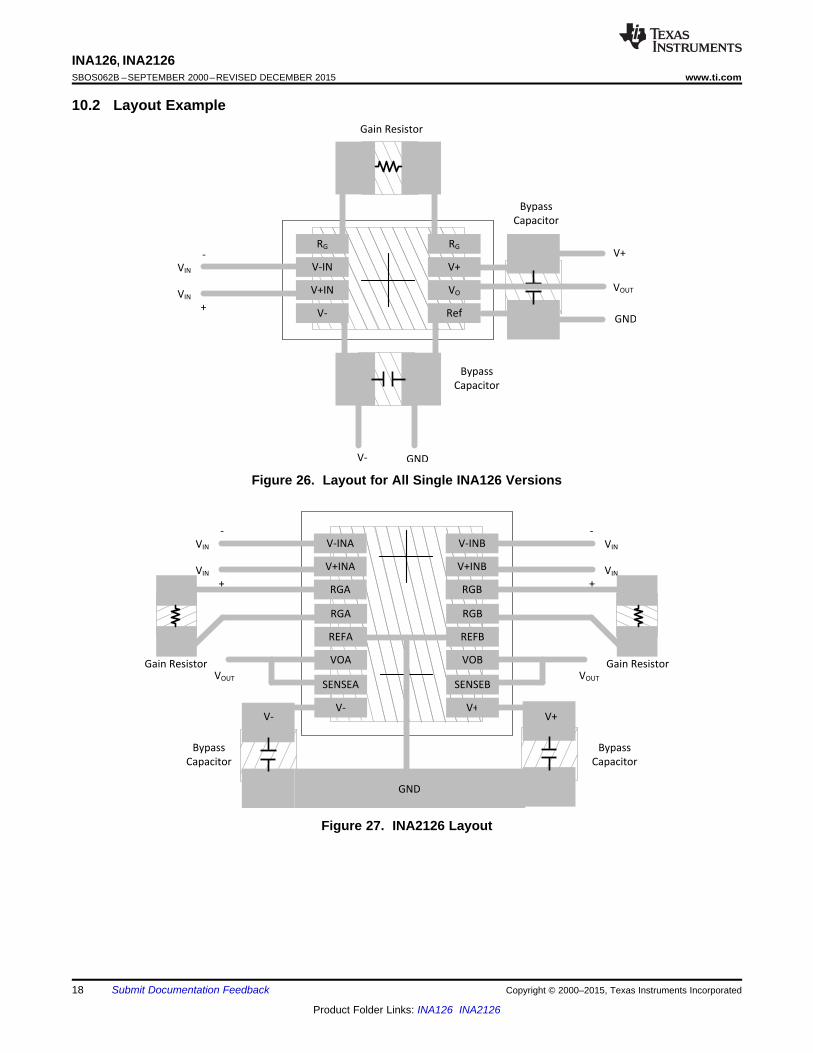
10.1 Layout GuidelinesAttention to good layout practices is always recommended. For best operational performance of the device, usegood printed circuit board (PCB) layout practices, including:• Take care to ensure that both input paths are well-matched for source impedance and capacitance to avoid
converting common-mode signals into differential signals. In addition, parasitic capacitance at the gain-settingpins can also affect CMRR over frequency. For example, in applications that implement gain switching usingswitches or PhotoMOS® relays to change the value of RG, select the component so that the switchcapacitance is as small as possible.– Connect low-ESR, 0.1-μF ceramic bypass capacitors between each supply pin and ground, placed as
close to the device as possible. A single bypass capacitor from V+ to ground is applicable for single-supply applications.
• Separate grounding for analog and digital portions of the circuitry is one of the simplest and most effectivemethods of noise suppression. One or more layers on multilayer PCBs are usually devoted to ground planes.A ground plane helps distribute heat and reduces EMI noise pickup. Make sure to physically separate digitaland analog grounds, paying attention to the flow of the ground current. For more detailed information, seeSLOA089, Circuit Board Layout Techniques.
• In order to reduce parasitic coupling, run the input traces as far away from the supply or output traces aspossible. If these traces cannot be kept separate, crossing the sensitive trace perpendicular is much betterthan in parallel with the noisy trace.
• Place the external components as close to the device as possible. As illustrated in Figure 26, keeping RGclose to the pins minimizes parasitic capacitance.
• Keep the traces as short as possible
Copyright © 2000–2015, Texas Instruments Incorporated Submit Documentation Feedback 17
Product Folder Links: INA126 INA2126
V-INB
V+INB
RGB
V-INA
V+INA
RGA
RGB
REFB
VOB
RGA
REFA
VOA
SENSEB
V+
SENSEA
V-
Bypass
Capacitor
Bypass
Capacitor
GND
V+V-
VIN
VIN
-
+
VOUT
Gain Resistor
VIN
VIN
-
+
VOUT
Gain Resistor
RG
V+
VO
Ref
RG
V-IN
V+IN
V-
VIN
VIN
-
+
V- GND
Bypass
Capacitor
Gain Resistor
Bypass
Capacitor
GND
V+
VOUT
INA126, INA2126SBOS062B –SEPTEMBER 2000–REVISED DECEMBER 2015 www.ti.com
10.2 Layout Example
Figure 26. Layout for All Single INA126 Versions
Figure 27. INA2126 Layout
18 Submit Documentation Feedback Copyright © 2000–2015, Texas Instruments Incorporated
Product Folder Links: INA126 INA2126
INA126, INA2126www.ti.com SBOS062B –SEPTEMBER 2000–REVISED DECEMBER 2015
11 Device and Documentation Support
11.1 Related LinksThe table below lists quick access links. Categories include technical documents, support and communityresources, tools and software, and quick access to sample or buy.
Table 1. Related LinksTECHNICAL TOOLS & SUPPORT &PARTS PRODUCT FOLDER SAMPLE & BUY DOCUMENTS SOFTWARE COMMUNITY
INA126 Click here Click here Click here Click here Click hereINA2126 Click here Click here Click here Click here Click here
11.2 Community ResourcesThe following links connect to TI community resources. Linked contents are provided "AS IS" by the respectivecontributors. They do not constitute TI specifications and do not necessarily reflect TI's views; see TI's Terms ofUse.
TI E2E™ Online Community TI's Engineer-to-Engineer (E2E) Community. Created to foster collaborationamong engineers. At e2e.ti.com, you can ask questions, share knowledge, explore ideas and helpsolve problems with fellow engineers.
Design Support TI's Design Support Quickly find helpful E2E forums along with design support tools andcontact information for technical support.
11.3 TrademarksE2E is a trademark of Texas Instruments.All other trademarks are the property of their respective owners.
11.4 Electrostatic Discharge CautionThese devices have limited built-in ESD protection. The leads should be shorted together or the device placed in conductive foamduring storage or handling to prevent electrostatic damage to the MOS gates.
11.5 GlossarySLYZ022 — TI Glossary.
This glossary lists and explains terms, acronyms, and definitions.
12 Mechanical, Packaging, and Orderable InformationThe following pages include mechanical, packaging, and orderable information. This information is the mostcurrent data available for the designated devices. This data is subject to change without notice and revision ofthis document. For browser-based versions of this data sheet, refer to the left-hand navigation.
Copyright © 2000–2015, Texas Instruments Incorporated Submit Documentation Feedback 19
Product Folder Links: INA126 INA2126
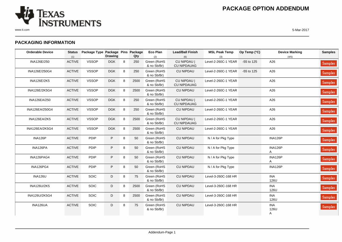
PACKAGE OPTION ADDENDUM
www.ti.com 5-Mar-2017
Addendum-Page 1
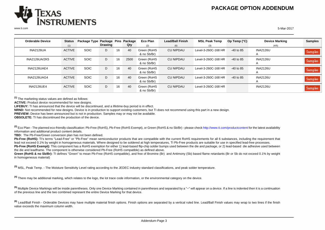
PACKAGING INFORMATION
Orderable Device Status(1)
Package Type PackageDrawing
Pins PackageQty
Eco Plan(2)
Lead/Ball Finish(6)
MSL Peak Temp(3)
Op Temp (°C) Device Marking(4/5)
Samples
INA126E/250 ACTIVE VSSOP DGK 8 250 Green (RoHS& no Sb/Br)
CU NIPDAU |CU NIPDAUAG
Level-2-260C-1 YEAR -55 to 125 A26
INA126E/250G4 ACTIVE VSSOP DGK 8 250 Green (RoHS& no Sb/Br)
CU NIPDAU Level-2-260C-1 YEAR -55 to 125 A26
INA126E/2K5 ACTIVE VSSOP DGK 8 2500 Green (RoHS& no Sb/Br)
CU NIPDAU |CU NIPDAUAG
Level-2-260C-1 YEAR A26
INA126E/2K5G4 ACTIVE VSSOP DGK 8 2500 Green (RoHS& no Sb/Br)
CU NIPDAU Level-2-260C-1 YEAR A26
INA126EA/250 ACTIVE VSSOP DGK 8 250 Green (RoHS& no Sb/Br)
CU NIPDAU |CU NIPDAUAG
Level-2-260C-1 YEAR A26
INA126EA/250G4 ACTIVE VSSOP DGK 8 250 Green (RoHS& no Sb/Br)
CU NIPDAU Level-2-260C-1 YEAR A26
INA126EA/2K5 ACTIVE VSSOP DGK 8 2500 Green (RoHS& no Sb/Br)
CU NIPDAU |CU NIPDAUAG
Level-2-260C-1 YEAR A26
INA126EA/2K5G4 ACTIVE VSSOP DGK 8 2500 Green (RoHS& no Sb/Br)
CU NIPDAU Level-2-260C-1 YEAR A26
INA126P ACTIVE PDIP P 8 50 Green (RoHS& no Sb/Br)
CU NIPDAU N / A for Pkg Type INA126P
INA126PA ACTIVE PDIP P 8 50 Green (RoHS& no Sb/Br)
CU NIPDAU N / A for Pkg Type INA126PA
INA126PAG4 ACTIVE PDIP P 8 50 Green (RoHS& no Sb/Br)
CU NIPDAU N / A for Pkg Type INA126PA
INA126PG4 ACTIVE PDIP P 8 50 Green (RoHS& no Sb/Br)
CU NIPDAU N / A for Pkg Type INA126P
INA126U ACTIVE SOIC D 8 75 Green (RoHS& no Sb/Br)
CU NIPDAU Level-3-260C-168 HR INA126U
INA126U/2K5 ACTIVE SOIC D 8 2500 Green (RoHS& no Sb/Br)
CU NIPDAU Level-3-260C-168 HR INA126U
INA126U/2K5G4 ACTIVE SOIC D 8 2500 Green (RoHS& no Sb/Br)
CU NIPDAU Level-3-260C-168 HR INA126U
INA126UA ACTIVE SOIC D 8 75 Green (RoHS& no Sb/Br)
CU NIPDAU Level-3-260C-168 HR INA126UA
PACKAGE OPTION ADDENDUM
www.ti.com 5-Mar-2017
Addendum-Page 2
Orderable Device Status(1)
Package Type PackageDrawing
Pins PackageQty
Eco Plan(2)
Lead/Ball Finish(6)
MSL Peak Temp(3)
Op Temp (°C) Device Marking(4/5)
Samples
INA126UA/2K5 ACTIVE SOIC D 8 2500 Green (RoHS& no Sb/Br)
CU NIPDAU Level-3-260C-168 HR INA126UA
INA126UAG4 ACTIVE SOIC D 8 75 Green (RoHS& no Sb/Br)
CU NIPDAU Level-3-260C-168 HR INA126UA
INA126UG4 ACTIVE SOIC D 8 75 Green (RoHS& no Sb/Br)
CU NIPDAU Level-3-260C-168 HR INA126U
INA2126E/250 ACTIVE SSOP DBQ 16 250 Green (RoHS& no Sb/Br)
Call TI Level-3-260C-168 HR INA2126EA
INA2126E/250G4 ACTIVE SSOP DBQ 16 250 Green (RoHS& no Sb/Br)
Call TI Level-3-260C-168 HR INA2126EA
INA2126E/2K5 ACTIVE SSOP DBQ 16 2500 Green (RoHS& no Sb/Br)
Call TI Level-3-260C-168 HR INA2126EA
INA2126E/2K5G4 ACTIVE SSOP DBQ 16 2500 Green (RoHS& no Sb/Br)
Call TI Level-3-260C-168 HR INA2126EA
INA2126EA/250 ACTIVE SSOP DBQ 16 250 Green (RoHS& no Sb/Br)
Call TI Level-3-260C-168 HR INA2126EA
INA2126EA/250G4 ACTIVE SSOP DBQ 16 250 Green (RoHS& no Sb/Br)
Call TI Level-3-260C-168 HR INA2126EA
INA2126EA/2K5 ACTIVE SSOP DBQ 16 2500 Green (RoHS& no Sb/Br)
Call TI Level-3-260C-168 HR INA2126EA
INA2126P OBSOLETE PDIP N 16 TBD Call TI Call TI INA2126P
INA2126PA OBSOLETE PDIP N 16 TBD Call TI Call TI INA2126PA
INA2126PAG4 OBSOLETE PDIP N 16 TBD Call TI Call TI INA2126PA
INA2126PG4 OBSOLETE PDIP N 16 TBD Call TI Call TI INA2126P
INA2126U ACTIVE SOIC D 16 40 Green (RoHS& no Sb/Br)
CU NIPDAU Level-3-260C-168 HR INA2126U
PACKAGE OPTION ADDENDUM
www.ti.com 5-Mar-2017
Addendum-Page 3
Orderable Device Status(1)
Package Type PackageDrawing
Pins PackageQty
Eco Plan(2)
Lead/Ball Finish(6)
MSL Peak Temp(3)
Op Temp (°C) Device Marking(4/5)
Samples
INA2126UA ACTIVE SOIC D 16 40 Green (RoHS& no Sb/Br)
CU NIPDAU Level-3-260C-168 HR -40 to 85 INA2126UA
INA2126UA/2K5 ACTIVE SOIC D 16 2500 Green (RoHS& no Sb/Br)
CU NIPDAU Level-3-260C-168 HR -40 to 85 INA2126UA
INA2126UAE4 ACTIVE SOIC D 16 40 Green (RoHS& no Sb/Br)
CU NIPDAU Level-3-260C-168 HR -40 to 85 INA2126UA
INA2126UAG4 ACTIVE SOIC D 16 40 Green (RoHS& no Sb/Br)
CU NIPDAU Level-3-260C-168 HR -40 to 85 INA2126UA
INA2126UE4 ACTIVE SOIC D 16 40 Green (RoHS& no Sb/Br)
CU NIPDAU Level-3-260C-168 HR INA2126U
(1) The marketing status values are defined as follows:ACTIVE: Product device recommended for new designs.LIFEBUY: TI has announced that the device will be discontinued, and a lifetime-buy period is in effect.NRND: Not recommended for new designs. Device is in production to support existing customers, but TI does not recommend using this part in a new design.PREVIEW: Device has been announced but is not in production. Samples may or may not be available.OBSOLETE: TI has discontinued the production of the device.
(2) Eco Plan - The planned eco-friendly classification: Pb-Free (RoHS), Pb-Free (RoHS Exempt), or Green (RoHS & no Sb/Br) - please check http://www.ti.com/productcontent for the latest availabilityinformation and additional product content details.TBD: The Pb-Free/Green conversion plan has not been defined.Pb-Free (RoHS): TI's terms "Lead-Free" or "Pb-Free" mean semiconductor products that are compatible with the current RoHS requirements for all 6 substances, including the requirement thatlead not exceed 0.1% by weight in homogeneous materials. Where designed to be soldered at high temperatures, TI Pb-Free products are suitable for use in specified lead-free processes.Pb-Free (RoHS Exempt): This component has a RoHS exemption for either 1) lead-based flip-chip solder bumps used between the die and package, or 2) lead-based die adhesive used betweenthe die and leadframe. The component is otherwise considered Pb-Free (RoHS compatible) as defined above.Green (RoHS & no Sb/Br): TI defines "Green" to mean Pb-Free (RoHS compatible), and free of Bromine (Br) and Antimony (Sb) based flame retardants (Br or Sb do not exceed 0.1% by weightin homogeneous material)
(3) MSL, Peak Temp. - The Moisture Sensitivity Level rating according to the JEDEC industry standard classifications, and peak solder temperature.
(4) There may be additional marking, which relates to the logo, the lot trace code information, or the environmental category on the device.
(5) Multiple Device Markings will be inside parentheses. Only one Device Marking contained in parentheses and separated by a "~" will appear on a device. If a line is indented then it is a continuationof the previous line and the two combined represent the entire Device Marking for that device.
(6) Lead/Ball Finish - Orderable Devices may have multiple material finish options. Finish options are separated by a vertical ruled line. Lead/Ball Finish values may wrap to two lines if the finishvalue exceeds the maximum column width.
PACKAGE OPTION ADDENDUM
www.ti.com 5-Mar-2017
Addendum-Page 4
Important Information and Disclaimer:The information provided on this page represents TI's knowledge and belief as of the date that it is provided. TI bases its knowledge and belief on informationprovided by third parties, and makes no representation or warranty as to the accuracy of such information. Efforts are underway to better integrate information from third parties. TI has taken andcontinues to take reasonable steps to provide representative and accurate information but may not have conducted destructive testing or chemical analysis on incoming materials and chemicals.TI and TI suppliers consider certain information to be proprietary, and thus CAS numbers and other limited information may not be available for release.
In no event shall TI's liability arising out of such information exceed the total purchase price of the TI part(s) at issue in this document sold by TI to Customer on an annual basis.
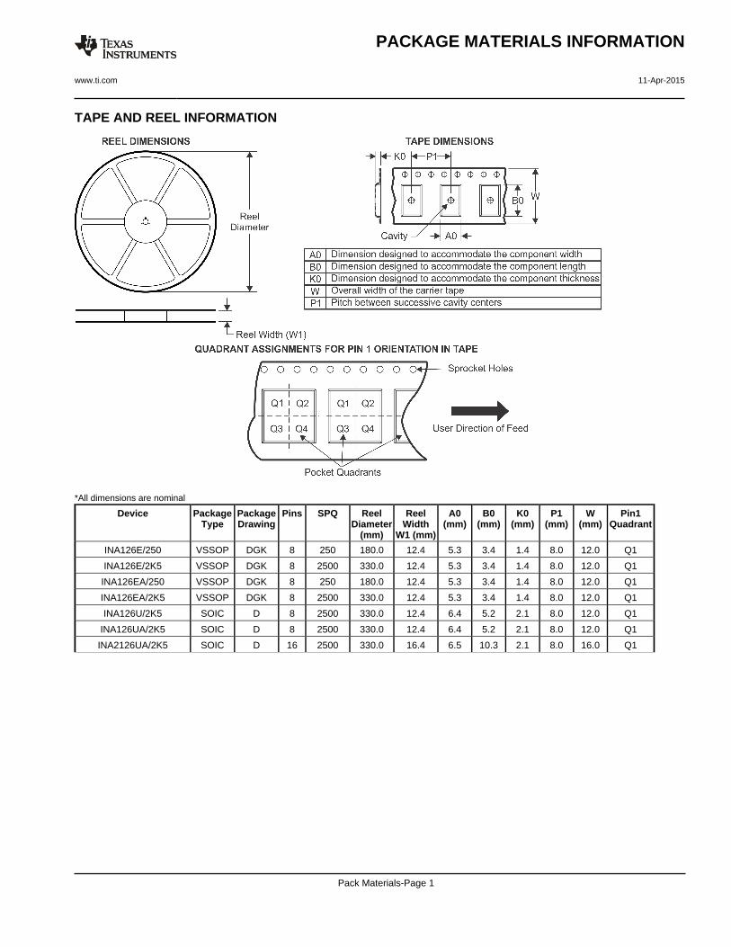
TAPE AND REEL INFORMATION
*All dimensions are nominal
Device PackageType
PackageDrawing
Pins SPQ ReelDiameter
(mm)
ReelWidth
W1 (mm)
A0(mm)
B0(mm)
K0(mm)
P1(mm)
W(mm)
Pin1Quadrant
INA126E/250 VSSOP DGK 8 250 180.0 12.4 5.3 3.4 1.4 8.0 12.0 Q1
INA126E/2K5 VSSOP DGK 8 2500 330.0 12.4 5.3 3.4 1.4 8.0 12.0 Q1
INA126EA/250 VSSOP DGK 8 250 180.0 12.4 5.3 3.4 1.4 8.0 12.0 Q1
INA126EA/2K5 VSSOP DGK 8 2500 330.0 12.4 5.3 3.4 1.4 8.0 12.0 Q1
INA126U/2K5 SOIC D 8 2500 330.0 12.4 6.4 5.2 2.1 8.0 12.0 Q1
INA126UA/2K5 SOIC D 8 2500 330.0 12.4 6.4 5.2 2.1 8.0 12.0 Q1
INA2126UA/2K5 SOIC D 16 2500 330.0 16.4 6.5 10.3 2.1 8.0 16.0 Q1
PACKAGE MATERIALS INFORMATION
www.ti.com 11-Apr-2015
Pack Materials-Page 1
*All dimensions are nominal
Device Package Type Package Drawing Pins SPQ Length (mm) Width (mm) Height (mm)
INA126E/250 VSSOP DGK 8 250 210.0 185.0 35.0
INA126E/2K5 VSSOP DGK 8 2500 367.0 367.0 35.0
INA126EA/250 VSSOP DGK 8 250 210.0 185.0 35.0
INA126EA/2K5 VSSOP DGK 8 2500 367.0 367.0 35.0
INA126U/2K5 SOIC D 8 2500 367.0 367.0 35.0
INA126UA/2K5 SOIC D 8 2500 367.0 367.0 35.0
INA2126UA/2K5 SOIC D 16 2500 367.0 367.0 38.0
PACKAGE MATERIALS INFORMATION
www.ti.com 11-Apr-2015
Pack Materials-Page 2
IMPORTANT NOTICE
Texas Instruments Incorporated (TI) reserves the right to make corrections, enhancements, improvements and other changes to itssemiconductor products and services per JESD46, latest issue, and to discontinue any product or service per JESD48, latest issue. Buyersshould obtain the latest relevant information before placing orders and should verify that such information is current and complete.TI’s published terms of sale for semiconductor products (http://www.ti.com/sc/docs/stdterms.htm) apply to the sale of packaged integratedcircuit products that TI has qualified and released to market. Additional terms may apply to the use or sale of other types of TI products andservices.Reproduction of significant portions of TI information in TI data sheets is permissible only if reproduction is without alteration and isaccompanied by all associated warranties, conditions, limitations, and notices. TI is not responsible or liable for such reproduceddocumentation. Information of third parties may be subject to additional restrictions. Resale of TI products or services with statementsdifferent from or beyond the parameters stated by TI for that product or service voids all express and any implied warranties for theassociated TI product or service and is an unfair and deceptive business practice. TI is not responsible or liable for any such statements.Buyers and others who are developing systems that incorporate TI products (collectively, “Designers”) understand and agree that Designersremain responsible for using their independent analysis, evaluation and judgment in designing their applications and that Designers havefull and exclusive responsibility to assure the safety of Designers' applications and compliance of their applications (and of all TI productsused in or for Designers’ applications) with all applicable regulations, laws and other applicable requirements. Designer represents that, withrespect to their applications, Designer has all the necessary expertise to create and implement safeguards that (1) anticipate dangerousconsequences of failures, (2) monitor failures and their consequences, and (3) lessen the likelihood of failures that might cause harm andtake appropriate actions. Designer agrees that prior to using or distributing any applications that include TI products, Designer willthoroughly test such applications and the functionality of such TI products as used in such applications.TI’s provision of technical, application or other design advice, quality characterization, reliability data or other services or information,including, but not limited to, reference designs and materials relating to evaluation modules, (collectively, “TI Resources”) are intended toassist designers who are developing applications that incorporate TI products; by downloading, accessing or using TI Resources in anyway, Designer (individually or, if Designer is acting on behalf of a company, Designer’s company) agrees to use any particular TI Resourcesolely for this purpose and subject to the terms of this Notice.TI’s provision of TI Resources does not expand or otherwise alter TI’s applicable published warranties or warranty disclaimers for TIproducts, and no additional obligations or liabilities arise from TI providing such TI Resources. TI reserves the right to make corrections,enhancements, improvements and other changes to its TI Resources. TI has not conducted any testing other than that specificallydescribed in the published documentation for a particular TI Resource.Designer is authorized to use, copy and modify any individual TI Resource only in connection with the development of applications thatinclude the TI product(s) identified in such TI Resource. NO OTHER LICENSE, EXPRESS OR IMPLIED, BY ESTOPPEL OR OTHERWISETO ANY OTHER TI INTELLECTUAL PROPERTY RIGHT, AND NO LICENSE TO ANY TECHNOLOGY OR INTELLECTUAL PROPERTYRIGHT OF TI OR ANY THIRD PARTY IS GRANTED HEREIN, including but not limited to any patent right, copyright, mask work right, orother intellectual property right relating to any combination, machine, or process in which TI products or services are used. Informationregarding or referencing third-party products or services does not constitute a license to use such products or services, or a warranty orendorsement thereof. Use of TI Resources may require a license from a third party under the patents or other intellectual property of thethird party, or a license from TI under the patents or other intellectual property of TI.TI RESOURCES ARE PROVIDED “AS IS” AND WITH ALL FAULTS. TI DISCLAIMS ALL OTHER WARRANTIES ORREPRESENTATIONS, EXPRESS OR IMPLIED, REGARDING RESOURCES OR USE THEREOF, INCLUDING BUT NOT LIMITED TOACCURACY OR COMPLETENESS, TITLE, ANY EPIDEMIC FAILURE WARRANTY AND ANY IMPLIED WARRANTIES OFMERCHANTABILITY, FITNESS FOR A PARTICULAR PURPOSE, AND NON-INFRINGEMENT OF ANY THIRD PARTY INTELLECTUALPROPERTY RIGHTS. TI SHALL NOT BE LIABLE FOR AND SHALL NOT DEFEND OR INDEMNIFY DESIGNER AGAINST ANY CLAIM,INCLUDING BUT NOT LIMITED TO ANY INFRINGEMENT CLAIM THAT RELATES TO OR IS BASED ON ANY COMBINATION OFPRODUCTS EVEN IF DESCRIBED IN TI RESOURCES OR OTHERWISE. IN NO EVENT SHALL TI BE LIABLE FOR ANY ACTUAL,DIRECT, SPECIAL, COLLATERAL, INDIRECT, PUNITIVE, INCIDENTAL, CONSEQUENTIAL OR EXEMPLARY DAMAGES INCONNECTION WITH OR ARISING OUT OF TI RESOURCES OR USE THEREOF, AND REGARDLESS OF WHETHER TI HAS BEENADVISED OF THE POSSIBILITY OF SUCH DAMAGES.Unless TI has explicitly designated an individual product as meeting the requirements of a particular industry standard (e.g., ISO/TS 16949and ISO 26262), TI is not responsible for any failure to meet such industry standard requirements.Where TI specifically promotes products as facilitating functional safety or as compliant with industry functional safety standards, suchproducts are intended to help enable customers to design and create their own applications that meet applicable functional safety standardsand requirements. Using products in an application does not by itself establish any safety features in the application. Designers mustensure compliance with safety-related requirements and standards applicable to their applications. Designer may not use any TI products inlife-critical medical equipment unless authorized officers of the parties have executed a special contract specifically governing such use.Life-critical medical equipment is medical equipment where failure of such equipment would cause serious bodily injury or death (e.g., lifesupport, pacemakers, defibrillators, heart pumps, neurostimulators, and implantables). Such equipment includes, without limitation, allmedical devices identified by the U.S. Food and Drug Administration as Class III devices and equivalent classifications outside the U.S.TI may expressly designate certain products as completing a particular qualification (e.g., Q100, Military Grade, or Enhanced Product).Designers agree that it has the necessary expertise to select the product with the appropriate qualification designation for their applicationsand that proper product selection is at Designers’ own risk. Designers are solely responsible for compliance with all legal and regulatoryrequirements in connection with such selection.Designer will fully indemnify TI and its representatives against any damages, costs, losses, and/or liabilities arising out of Designer’s non-compliance with the terms and provisions of this Notice.
Mailing Address: Texas Instruments, Post Office Box 655303, Dallas, Texas 75265Copyright © 2017, Texas Instruments Incorporated