IEEE ELECTRON DEVICE LETTERS, VOL. 33, NO. 4, …hxing/research/pdfs/12-edl-Guo-MBE regrown...
3
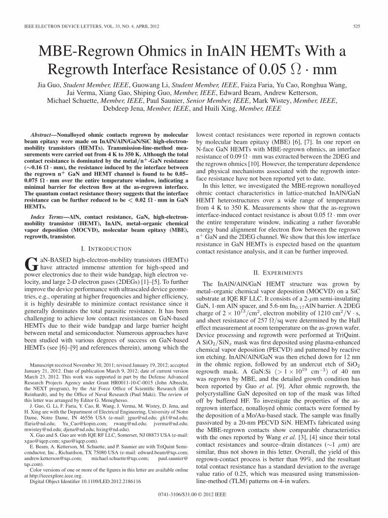
IEEE ELECTRON DEVICE LETTERS, VOL. 33, NO. 4, APRIL 2012 525 MBE-Regrown Ohmics in InAlN HEMTs With a Regrowth Interface Resistance of 0.05 Ω · mm Jia Guo, Student Member, IEEE, Guowang Li, Student Member, IEEE, Faiza Faria, Yu Cao, Ronghua Wang, Jai Verma, Xiang Gao, Shiping Guo, Member, IEEE, Edward Beam, Andrew Ketterson, Michael Schuette, Member, IEEE, Paul Saunier, Senior Member, IEEE, Mark Wistey, Member, IEEE, Debdeep Jena, Member, IEEE, and Huili Xing, Member, IEEE Abstract—Nonalloyed ohmic contacts regrown by molecular beam epitaxy were made on InAlN/AlN/GaN/SiC high-electron- mobility transistors (HEMTs). Transmission-line-method mea- surements were carried out from 4 K to 350 K. Although the total contact resistance is dominated by the metal/n + -GaN resistance (∼0.16 Ω · mm), the resistance induced by the interface between the regrown n + GaN and HEMT channel is found to be 0.05– 0.075 Ω · mm over the entire temperature window, indicating a minimal barrier for electron flow at the as-regrown interface. The quantum contact resistance theory suggests that the interface resistance can be further reduced to be < 0.02 Ω · mm in GaN HEMTs. Index Terms—AlN, contact resistance, GaN, high-electron- mobility transistor (HEMT), InAlN, metal–organic chemical vapor deposition (MOCVD), molecular beam epitaxy (MBE), regrowth, transistor. I. I NTRODUCTION G aN-BASED high-electron-mobility transistors (HEMTs) have attracted immense attention for high-speed and power electronics due to their wide bandgap, high electron ve- locity, and large 2-D electron gases (2DEGs) [1]–[5]. To further improve the device performance with ultrascaled device geome- tries, e.g., operating at higher frequencies and higher efficiency, it is highly desirable to minimize contact resistance since it generally dominates the total parasitic resistance. It has been challenging to achieve low contact resistances on GaN-based HEMTs due to their wide bandgap and large barrier height between metal and semiconductor. Numerous approaches have been studied with various degrees of success on GaN-based HEMTs (see [6]–[9] and references therein), among which the Manuscript received November 30, 2011; revised January 19, 2012; accepted January 21, 2012. Date of publication March 9, 2012; date of current version March 23, 2012. This work was supported in part by the Defense Advanced Research Projects Agency under Grant HR0011-10-C-0015 (John Albrecht, the NEXT program), by the Air Force Office of Scientific Research (Kitt Reinhardt), and by the Office of Naval Research (Paul Maki). The review of this letter was arranged by Editor G. Meneghesso. J. Guo, G. Li, F. Faria, Y. Cao, R. Wang, J. Verma, M. Wistey, D. Jena, and H. Xing are with the Department of Electrical Engineering, University of Notre Dame, Notre Dame, IN 46556 USA (e-mail: [email protected]; [email protected]; [email protected]; [email protected]; [email protected]; [email protected]; [email protected]; [email protected]; [email protected]). X. Gao and S. Guo are with IQE RF LLC, Somerset, NJ 08873 USA (e-mail: [email protected]; [email protected]). E. Beam, A. Ketterson, M. Schuette, and P. Saunier are with TriQuint Semi- conductor, Inc., Richardson, TX 75080 USA (e-mail: [email protected]; [email protected]; [email protected]; paul.saunier@ tqs.com). Color versions of one or more of the figures in this letter are available online at http://ieeexplore.ieee.org. Digital Object Identifier 10.1109/LED.2012.2186116 lowest contact resistances were reported in regrown contacts by molecular beam epitaxy (MBE) [6], [7]. In one report on N-face GaN HEMTs with MBE-regrown ohmics, an interface resistance of 0.09 Ω · mm was extracted between the 2DEG and the regrown ohmics [10]. However, the temperature dependence and physical mechanisms associated with the regrowth inter- face resistance have not been reported yet to date. In this letter, we investigated the MBE-regrown nonalloyed ohmic contact characteristics in lattice-matched InAlN/GaN HEMT heterostructures over a wide range of temperatures from 4 K to 350 K. Measurements show that the as-regrown interface-induced contact resistance is about 0.05 Ω · mm over the entire temperature window, indicating a rather favorable energy band alignment for electron flow between the regrown n + GaN and the 2DEG channel. We show that this low interface resistance in GaN HEMTs is expected based on the quantum contact resistance analysis, and it can be further improved. II. EXPERIMENTS The InAlN/AlN/GaN HEMT structure was grown by metal–organic chemical vapor deposition (MOCVD) on a SiC substrate at IQE RF LLC. It consists of a 2-µm semi-insulating GaN, 1-nm AlN spacer, and 5.6-nm In 0.17 AlN barrier. A 2DEG charge of 2 × 10 13 /cm 2 , electron mobility of 1210 cm 2 /V · s, and sheet resistance of 257 Ω/sq were determined by the Hall effect measurement at room temperature on the as-grown wafer. Device processing and regrowth were performed at TriQuint. A SiO 2 /SiN x mask was first deposited using plasma-enhanced chemical vapor deposition (PECVD) and patterned by reactive ion etching. InAlN/AlN/GaN was then etched down for 12 nm in the ohmic region, followed by an undercut etch of SiO 2 regrowth mask. A GaN:Si (> 1 × 10 19 cm −3 ) of 40 nm was regrown by MBE, and the detailed growth condition has been reported by Guo et al. [9]. After ohmic regrowth, the polycrystalline GaN deposited on top of the mask was lifted off by buffered HF. To investigate the properties of the as- regrown interface, nonalloyed ohmic contacts were formed by the deposition of a Mo/Au-based stack. The sample was finally passivated by a 20-nm PECVD SiN. HEMTs fabricated using the MBE-regrown contacts show comparable characteristics with the ones reported by Wang et al. [3], [4] since their total contact resistances and source–drain distances (∼1 µm) are similar, thus not shown in this letter. Overall, the yield of this regrown-contact process is better than 99%, and the resultant total contact resistance has a standard deviation to the average value ratio of 0.25, which was measured using transmission- line-method (TLM) patterns on 4-in wafers. 0741-3106/$31.00 © 2012 IEEE
Transcript of IEEE ELECTRON DEVICE LETTERS, VOL. 33, NO. 4, …hxing/research/pdfs/12-edl-Guo-MBE regrown...
IEEE ELECTRON DEVICE LETTERS, VOL. 33, NO. 4, APRIL 2012 525
MBE-Regrown Ohmics in InAlN HEMTs With aRegrowth Interface Resistance of 0.05 Ω · mm
Jia Guo, Student Member, IEEE, Guowang Li, Student Member, IEEE, Faiza Faria, Yu Cao, Ronghua Wang,Jai Verma, Xiang Gao, Shiping Guo, Member, IEEE, Edward Beam, Andrew Ketterson,
Michael Schuette, Member, IEEE, Paul Saunier, Senior Member, IEEE, Mark Wistey, Member, IEEE,Debdeep Jena, Member, IEEE, and Huili Xing, Member, IEEE
Abstract—Nonalloyed ohmic contacts regrown by molecularbeam epitaxy were made on InAlN/AlN/GaN/SiC high-electron-mobility transistors (HEMTs). Transmission-line-method mea-surements were carried out from 4 K to 350 K. Although the totalcontact resistance is dominated by the metal/n+-GaN resistance(∼0.16 Ω · mm), the resistance induced by the interface betweenthe regrown n+ GaN and HEMT channel is found to be 0.05–0.075 Ω · mm over the entire temperature window, indicating aminimal barrier for electron flow at the as-regrown interface.The quantum contact resistance theory suggests that the interfaceresistance can be further reduced to be < 0.02 Ω · mm in GaNHEMTs.
Index Terms—AlN, contact resistance, GaN, high-electron-mobility transistor (HEMT), InAlN, metal–organic chemicalvapor deposition (MOCVD), molecular beam epitaxy (MBE),regrowth, transistor.
I. INTRODUCTION
G aN-BASED high-electron-mobility transistors (HEMTs)have attracted immense attention for high-speed and
power electronics due to their wide bandgap, high electron ve-locity, and large 2-D electron gases (2DEGs) [1]–[5]. To furtherimprove the device performance with ultrascaled device geome-tries, e.g., operating at higher frequencies and higher efficiency,it is highly desirable to minimize contact resistance since itgenerally dominates the total parasitic resistance. It has beenchallenging to achieve low contact resistances on GaN-basedHEMTs due to their wide bandgap and large barrier heightbetween metal and semiconductor. Numerous approaches havebeen studied with various degrees of success on GaN-basedHEMTs (see [6]–[9] and references therein), among which the
Manuscript received November 30, 2011; revised January 19, 2012; acceptedJanuary 21, 2012. Date of publication March 9, 2012; date of current versionMarch 23, 2012. This work was supported in part by the Defense AdvancedResearch Projects Agency under Grant HR0011-10-C-0015 (John Albrecht,the NEXT program), by the Air Force Office of Scientific Research (KittReinhardt), and by the Office of Naval Research (Paul Maki). The review ofthis letter was arranged by Editor G. Meneghesso.
J. Guo, G. Li, F. Faria, Y. Cao, R. Wang, J. Verma, M. Wistey, D. Jena, andH. Xing are with the Department of Electrical Engineering, University of NotreDame, Notre Dame, IN 46556 USA (e-mail: [email protected]; [email protected];[email protected]; [email protected]; [email protected]; [email protected];[email protected]; [email protected]; [email protected]).
X. Gao and S. Guo are with IQE RF LLC, Somerset, NJ 08873 USA (e-mail:[email protected]; [email protected]).
E. Beam, A. Ketterson, M. Schuette, and P. Saunier are with TriQuint Semi-conductor, Inc., Richardson, TX 75080 USA (e-mail: [email protected];[email protected]; [email protected]; [email protected]).
Color versions of one or more of the figures in this letter are available onlineat http://ieeexplore.ieee.org.
Digital Object Identifier 10.1109/LED.2012.2186116
lowest contact resistances were reported in regrown contactsby molecular beam epitaxy (MBE) [6], [7]. In one report onN-face GaN HEMTs with MBE-regrown ohmics, an interfaceresistance of 0.09 Ω · mm was extracted between the 2DEG andthe regrown ohmics [10]. However, the temperature dependenceand physical mechanisms associated with the regrowth inter-face resistance have not been reported yet to date.
In this letter, we investigated the MBE-regrown nonalloyedohmic contact characteristics in lattice-matched InAlN/GaNHEMT heterostructures over a wide range of temperaturesfrom 4 K to 350 K. Measurements show that the as-regrowninterface-induced contact resistance is about 0.05 Ω · mm overthe entire temperature window, indicating a rather favorableenergy band alignment for electron flow between the regrownn+ GaN and the 2DEG channel. We show that this low interfaceresistance in GaN HEMTs is expected based on the quantumcontact resistance analysis, and it can be further improved.
II. EXPERIMENTS
The InAlN/AlN/GaN HEMT structure was grown bymetal–organic chemical vapor deposition (MOCVD) on a SiCsubstrate at IQE RF LLC. It consists of a 2-µm semi-insulatingGaN, 1-nm AlN spacer, and 5.6-nm In0.17AlN barrier. A 2DEGcharge of 2 × 10¹³/cm2, electron mobility of 1210 cm2/V · s,and sheet resistance of 257 Ω/sq were determined by the Halleffect measurement at room temperature on the as-grown wafer.Device processing and regrowth were performed at TriQuint.A SiO2/SiNx mask was first deposited using plasma-enhancedchemical vapor deposition (PECVD) and patterned by reactiveion etching. InAlN/AlN/GaN was then etched down for 12 nmin the ohmic region, followed by an undercut etch of SiO2
regrowth mask. A GaN:Si (> 1 × 1019 cm−3) of 40 nmwas regrown by MBE, and the detailed growth condition hasbeen reported by Guo et al. [9]. After ohmic regrowth, thepolycrystalline GaN deposited on top of the mask was liftedoff by buffered HF. To investigate the properties of the as-regrown interface, nonalloyed ohmic contacts were formed bythe deposition of a Mo/Au-based stack. The sample was finallypassivated by a 20-nm PECVD SiN. HEMTs fabricated usingthe MBE-regrown contacts show comparable characteristicswith the ones reported by Wang et al. [3], [4] since their totalcontact resistances and source–drain distances (∼1 µm) aresimilar, thus not shown in this letter. Overall, the yield of thisregrown-contact process is better than 99%, and the resultanttotal contact resistance has a standard deviation to the averagevalue ratio of 0.25, which was measured using transmission-line-method (TLM) patterns on 4-in wafers.
0741-3106/$31.00 © 2012 IEEE
526 IEEE ELECTRON DEVICE LETTERS, VOL. 33, NO. 4, APRIL 2012
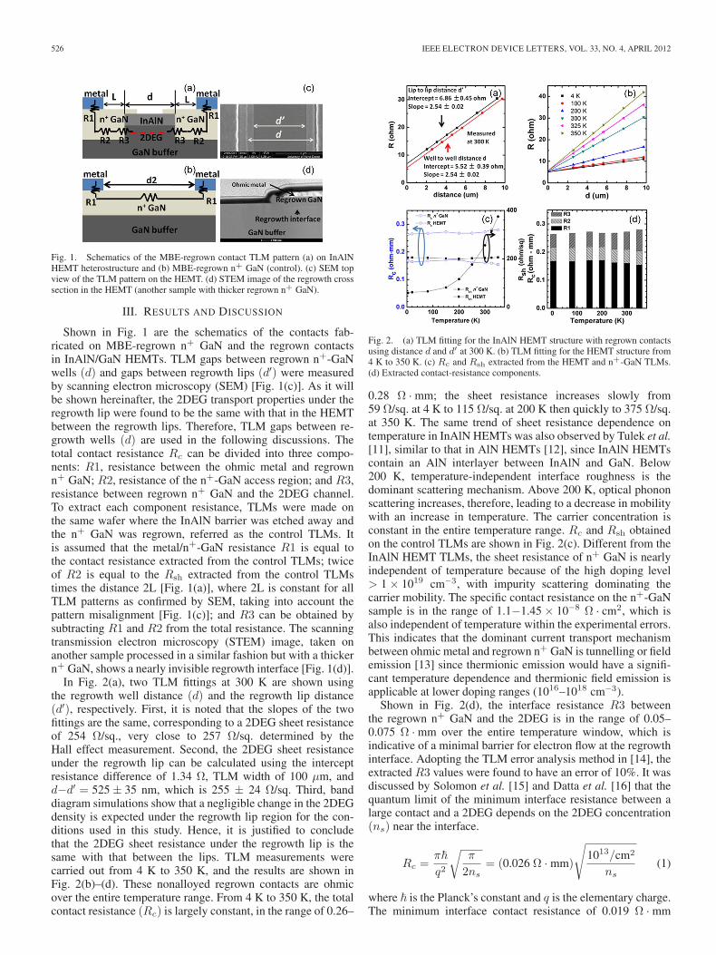
Fig. 1. Schematics of the MBE-regrown contact TLM pattern (a) on InAlNHEMT heterostructure and (b) MBE-regrown n+ GaN (control). (c) SEM topview of the TLM pattern on the HEMT. (d) STEM image of the regrowth crosssection in the HEMT (another sample with thicker regrown n+ GaN).
III. RESULTS AND DISCUSSION
Shown in Fig. 1 are the schematics of the contacts fab-ricated on MBE-regrown n+ GaN and the regrown contactsin InAlN/GaN HEMTs. TLM gaps between regrown n+-GaNwells (d) and gaps between regrowth lips (d′) were measuredby scanning electron microscopy (SEM) [Fig. 1(c)]. As it willbe shown hereinafter, the 2DEG transport properties under theregrowth lip were found to be the same with that in the HEMTbetween the regrowth lips. Therefore, TLM gaps between re-growth wells (d) are used in the following discussions. Thetotal contact resistance Rc can be divided into three compo-nents: R1, resistance between the ohmic metal and regrownn+ GaN; R2, resistance of the n+-GaN access region; and R3,resistance between regrown n+ GaN and the 2DEG channel.To extract each component resistance, TLMs were made onthe same wafer where the InAlN barrier was etched away andthe n+ GaN was regrown, referred as the control TLMs. Itis assumed that the metal/n+-GaN resistance R1 is equal tothe contact resistance extracted from the control TLMs; twiceof R2 is equal to the Rsh extracted from the control TLMstimes the distance 2L [Fig. 1(a)], where 2L is constant for allTLM patterns as confirmed by SEM, taking into account thepattern misalignment [Fig. 1(c)]; and R3 can be obtained bysubtracting R1 and R2 from the total resistance. The scanningtransmission electron microscopy (STEM) image, taken onanother sample processed in a similar fashion but with a thickern+ GaN, shows a nearly invisible regrowth interface [Fig. 1(d)].
In Fig. 2(a), two TLM fittings at 300 K are shown usingthe regrowth well distance (d) and the regrowth lip distance(d′), respectively. First, it is noted that the slopes of the twofittings are the same, corresponding to a 2DEG sheet resistanceof 254 Ω/sq., very close to 257 Ω/sq. determined by theHall effect measurement. Second, the 2DEG sheet resistanceunder the regrowth lip can be calculated using the interceptresistance difference of 1.34 Ω, TLM width of 100 µm, andd−d′ = 525 ± 35 nm, which is 255 ± 24 Ω/sq. Third, banddiagram simulations show that a negligible change in the 2DEGdensity is expected under the regrowth lip region for the con-ditions used in this study. Hence, it is justified to concludethat the 2DEG sheet resistance under the regrowth lip is thesame with that between the lips. TLM measurements werecarried out from 4 K to 350 K, and the results are shown inFig. 2(b)–(d). These nonalloyed regrown contacts are ohmicover the entire temperature range. From 4 K to 350 K, the totalcontact resistance (Rc) is largely constant, in the range of 0.26–
Fig. 2. (a) TLM fitting for the InAlN HEMT structure with regrown contactsusing distance d and d′ at 300 K. (b) TLM fitting for the HEMT structure from4 K to 350 K. (c) Rc and Rsh extracted from the HEMT and n+-GaN TLMs.(d) Extracted contact-resistance components.
0.28 Ω · mm; the sheet resistance increases slowly from59 Ω/sq. at 4 K to 115 Ω/sq. at 200 K then quickly to 375 Ω/sq.at 350 K. The same trend of sheet resistance dependence ontemperature in InAlN HEMTs was also observed by Tulek et al.[11], similar to that in AlN HEMTs [12], since InAlN HEMTscontain an AlN interlayer between InAlN and GaN. Below200 K, temperature-independent interface roughness is thedominant scattering mechanism. Above 200 K, optical phononscattering increases, therefore, leading to a decrease in mobilitywith an increase in temperature. The carrier concentration isconstant in the entire temperature range. Rc and Rsh obtainedon the control TLMs are shown in Fig. 2(c). Different from theInAlN HEMT TLMs, the sheet resistance of n+ GaN is nearlyindependent of temperature because of the high doping level> 1 × 1019 cm−3, with impurity scattering dominating thecarrier mobility. The specific contact resistance on the n+-GaNsample is in the range of 1.1−1.45 × 10⁻⁸ Ω · cm2, which isalso independent of temperature within the experimental errors.This indicates that the dominant current transport mechanismbetween ohmic metal and regrown n+ GaN is tunnelling or fieldemission [13] since thermionic emission would have a signifi-cant temperature dependence and thermionic field emission isapplicable at lower doping ranges (1016–1018 cm−3).
Shown in Fig. 2(d), the interface resistance R3 betweenthe regrown n+ GaN and the 2DEG is in the range of 0.05–0.075 Ω · mm over the entire temperature window, which isindicative of a minimal barrier for electron flow at the regrowthinterface. Adopting the TLM error analysis method in [14], theextracted R3 values were found to have an error of 10%. It wasdiscussed by Solomon et al. [15] and Datta et al. [16] that thequantum limit of the minimum interface resistance between alarge contact and a 2DEG depends on the 2DEG concentration(ns) near the interface.
Rc =π
q2
√π
2ns= (0.026 Ω · mm)
√1013/cm2
ns(1)
where is the Planck’s constant and q is the elementary charge.The minimum interface contact resistance of 0.019 Ω · mm
GUO et al.: MBE-REGROWN OHMICS IN InAlN HEMTs 527
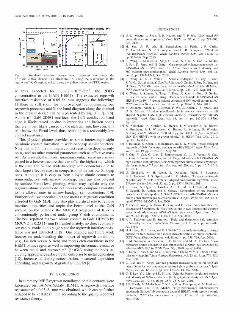
Fig. 3. Simulated electron energy band diagrams (a) along then+ GaN–2DEG channel (x) directions, (b) along the y-direction in theregrown-n+-GaN region, and (c) along the y-direction in the 2DEG region.
is thus expected for ns = 2 × 10¹³/cm2, the 2DEGconcentration in the InAlN HEMTs. The extracted regrowthinterface resistance of 0.05 Ω · mm suggests the following:1) there is still room for improvement by optimizing ourregrowth processes and 2) the band diagram along the channelin the present device can be represented by Fig. 3 [17], [18].At the n+ GaN–2DEG interface, the GaN conduction bandedge is likely raised up due to impurities and broken bondsthat are in part likely caused by the etch damage; however, it isstill below the Fermi level, thus, resulting in a reasonably lowcontact resistance.
This physical picture provides us some interesting insighton ohmic contact formation in wide-bandgap semiconductors.Note that in (1), the minimum contact resistance depends onlyon ns and no other material parameters such as effective massm∗. As a result, the lowest quantum contact resistance is ex-pected in a heterostructure that can offer the highest ns, whichis the case for Si and wide-bandgap semiconductors due totheir large effective mass in comparison to the narrow-bandgapones. Although it is easy to form alloyed ohmic contacts tosemiconductors with narrow bandgap, they are also plaguedby surface Fermi-level pinning, which may explain why theregrown ohmic contacts do not necessarily compare favorablyto the alloyed ones in narrow-bandgap semiconductors [19].Furthermore, we speculate that the metal-rich growth conditionafforded by GaN MBE may also play a critical role to removeinterface impurities and unpin the Fermi level at the GaNsurface; on the contrary, the MOCVD (re)growth of III-V isconventionally performed under group-V rich environments.The best reported regrown ohmic contact in GaN HEMTs byMOCVD is 0.23 Ω · mm [8]; unfortunately, no direct compari-son can be made at this stage since the regrowth interface resis-tance was not extracted in [8]. Our ongoing and future workfocuses on understanding the impact of regrowth conditions(e.g., Ga rich versus N rich) and recess etch conditions in theHEMT ohmic region as well as improving the contact resistancebetween metal and regrown n+ (In)GaN using methods in-cluding appropriate surface treatments prior to metal deposition[18], increase of doping concentration, postmetal depositionannealing, and regrowth of graded n+ InGaN [6].
IV. CONCLUSION
In summary, MBE-regrown nonalloyed ohmic contacts werefabricated on InAlN/AlN/GaN HEMTs. A regrowth interfaceresistance of ∼0.05 Ω · mm was obtained, which can be furtherreduced to be < 0.02 Ω · mm according to the quantum contactresistance theory.
REFERENCES
[1] U. K. Mishra, L. Shen, T. E. Kazior, and Y. F. Wu, “GaN-based RFpower devices and amplifiers,” Proc. IEEE, vol. 96, no. 2, pp. 287–305,Feb. 2008.
[2] H. Sun, A. R. Alt, H. Benedickter, E. Feltin, J.-F. Carlin,M. Gonschorek, N. R. Grandjean, and C. R. Bolognesi, “205-GHz(Al, In)N/GaN HEMTs,” IEEE Electron Device Lett., vol. 31, no. 9,pp. 957–959, Sep. 2010.
[3] R. Wang, P. Saunier, X. Xing, C. Lian, X. Gao, S. Guo, G. Snider,P. Fay, D. Jena, and H. Xing, “Gate-recessed enhancement-mode In-AlN/AlN/GaN HEMTs with 1.9 A/mm drain current density and800 mS/mm transconductance,” IEEE Electron Device Lett., vol. 31,no. 12, pp. 1383–1385, Dec. 2010.
[4] R. Wang, G. Li, J. Verma, B. Sensale-Rodriguez, T. Fang, J. Guo,Z. Y. Hu, O. Laboutin, Y. Cao, W. Johnson, G. Snider, P. Fay, D. Jena, andH. Xing, “220-GHz quaternary barrier InAlNGaN/AlN/GaN HEMTs,”IEEE Electron Device Lett., vol. 32, no. 9, pp. 1215–1217, Sep. 2011.
[5] R. Wang, P. Saunier, Y. Tang, T. Fang, X. Gao, S. Guo, G. Snider,P. Fay, D. Jena, and H. Xing, “Enhancement-mode InAlN/AlN/GaNHEMTs with 10−12 A/mm leakage current and 1012 on/off current ratio,”IEEE Electron Device Lett., vol. 32, no. 3, pp. 309–311, Mar. 2011.
[6] S. Dasgupta, Nidhi, D. F. Brown, F. Wu, S. Keller, J. S. Speck, andU. K. Mishra, “Ultralow nonalloyed ohmic contact resistance to selfaligned N-polar GaN high electron mobility transistors by In(Ga)Nregrowth,” Appl. Phys. Lett., vol. 96, no. 14, pp. 143 504–143 506,Apr. 2010.
[7] K. Shinohara, A. Corrion, D. Regan, I. Milosavljevic, D. Brown,S. Burnham, P. J. Willadsen, C. Butler, A. Schmitz, D. Wheeler,A. Fung, and M. Micovic, “220 GHz fT and 400 GHz fmax in 40-nmGaN DH-HEMTs with re-grown ohmic,” in IEDM Tech. Dig., 2010,pp. 30.1.1–30.1.4.
[8] S. Heikman, S. Keller, S. P. DenBaars, and U. K. Mishra, “Mass transportregrowth of GaN for ohmic contacts to AlGaN/GaN,” Appl. Phys. Lett.,vol. 78, no. 19, pp. 2876–2878, May 2001.
[9] J. Guo, Y. Cao, C. Lian, T. Zimmermann, G. Li, J. Verma, X. Gao,S. Guo, P. Saunier, D. Jena, and H. Xing, “Metal-face InAlN/AlN/GaNhigh electron mobility transistors with regrown ohmic contacts by molec-ular beam epitaxy,” Phys. Stat. Sol. (A), vol. 208, no. 7, pp. 1617–1619,Jul. 2011.
[10] U. Singisetti, M. H. Wong, S. Dasgupta, Nidhi, B. Swenson,B. J. Thibeault, J. S. Speck, and U. K. Mishra, “Enhancement-modeN-polar GaN MISFETs with self-aligned source/drain regrowth,” IEEEElectron Device Lett., vol. 32, no. 2, pp. 137–139, Feb. 2011.
[11] R. Tulek, A. Llgaz, S. Gokden, A. Teke, M. K. Ozturk, M. Kasap,S. Ozcelik, E. Arslan, and E. Ozbay, “Comparison of the transportproperties of high quality AlGaN/AlN/GaN and AlInN/AlN/GaN two-dimensional electron gas heterostructures,” J. Appl. Phys., vol. 105, no. 1,pp. 013707-1–013707-6, Jan. 2009.
[12] Y. Cao, K. Wang, A. Orlov, H. Xing, and D. Jena, “Very low sheet re-sistance and Shubnikov-de-Haas oscillations in two-dimensional electrongases at ultrathin binary AlN/GaN heterojunctions,” Appl. Phys. Lett.,vol. 92, no. 15, pp. 152112-1–152112-3, Apr. 2008.
[13] F. A. Padovani and R. Stratton, “Field and thermionic-field emissionin Schottky barriers,” Solid State Electron., vol. 9, no. 7, pp. 695–707,Jul. 1966.
[14] H.-J. Ueng, D. B. Janes, and K. J. Webb, “Error analysis leading to designcriteria for transmission line model characterization of ohmic contacts,”IEEE Trans. Electron Devices, vol. 48, no. 4, pp. 758–766, Apr. 2001.
[15] P. M. Solomon, A. Palevski, T. F. Kuech, and M. A. Tischler, “Lowresistance ohmic contacts to two-dimensional electron-gas structures byselective MOVPE,” in IEDM Tech. Dig., 1989, pp. 405–408.
[16] S. Datta, F. Assad, and M. S. Lundstrom, “The Si MOSFET from a trans-mission viewpoint,” Superlattice Microstruct., vol. 23, no. 3, pp. 771–780,Mar. 1998.
[17] C. Lian and H. Xing, “Surface potential measurements on Ni-(Al)GaNlateral Schottky junction using scanning kelvin probe microscopy,” Appl.Phys. Lett., vol. 88, no. 2, pp. 022112–022114, Jan. 2006.
[18] C.-T. Lee, Y.-J. Lin, and D.-S. Liu, “Schottky barrier height and surfacestate density of Ni/Au contacts to (NH4)2Sx-treated n-type GaN,” Appl.Phys. Lett., vol. 79, no. 16, pp. 2573–2575, Oct. 2001.
[19] J. B. Shealy, M. Matloubian, T. Y. Liu, M. A. Thompson, M. M. Hashemi,S. DenBaars, and U. K. Mishra, “High-performance submicrometergatelength GaInAs/InP composite channel HEMTs with regrown ohmiccontacts,” IEEE Electron Device Lett., vol. 17, no. 11, pp. 540–542,Nov. 1996.