IC DATA SHEET - digchip.com · TOKO Inc. IC Data Sheet TK717xx GC3-H006C Page - 4 - Absolute...
23
IC DATA SHEET LDO REGULATOR WITH ON/OFF SWITCH TK717xx MEETING YOUR NEEDS
Transcript of IC DATA SHEET - digchip.com · TOKO Inc. IC Data Sheet TK717xx GC3-H006C Page - 4 - Absolute...
IC DATA SHEET
LDO REGULATOR WITH ON/OFF SWITCHTK717xx
MEETING YOUR NEEDS
TOKO Inc. IC Data Sheet TK717xx
GC3-H006C Page - 2 -
TK717xx
Features
・Built-in shunt circuit of output to GND. Charged energy of output capacitor isdischarged quickly.
・Built-in PNP power transistor. Very small Dropout Voltage(Vdrop=163mV at Iout=200mA)
・Very good stability (CL=0.22μF is stable for any type capacitor with 2.0V≦Vout)
・High accuracy out put voltage(±50mV or±1.5%)
・Good ripple rejection ratio(80dB at 1KHz Iout=10mA)
・Wide operating voltage range (1.8V~14V)
・Built-in short circuit protection
・Built-in over temperature protection
・Suitable for low noise applications
・Available with on/off control (High/on). Off time input current becomes pA level
・Very small package
DescriptionThe TK717xx is an integrated circuit with a silicon monolithic bipolar structure. The regulator is of the
low saturation voltage output type with very little quiescent current (72μA).
The PNP power transistor is built-in. The I/O voltage difference is 163 mV (typical) when a current of
200mA is supplied to the system. Because of the low voltage drop, the voltage source can be effectively
used; this makes it very suitable for battery powered equipment.
The on/off function is built into the IC. The current during standby mode becomes very small (pA level).
In addition, the output short-circuit function works at off times. It is a unique characteristic by
which the residual charge of the output side capacitor is rapidly discharged.
The output voltage is available from 1.5 to 10.0V in 0.1V steps. The output voltage is trimmed with high
accuracy. This allows the optimum voltage to be selected for the equipment.
The over current sensor circuit and the reverse-bias protection circuit are built-in.
It is a very rugged design because the ESD protection is high. Therefore, the TK717xx can be used with
confidence. When mounted on the PCB, the power dissipation rating becomes about 500mW, even
though the package is very small.
The TK717xx features very high stability in both DC and AC. The capacitor on the output side provides
stable operation with 0.22μF with 2.0V≦Vout. A capacitor of any type can be used; however, the
larger this capacitor is, the better the overall characteristics are.
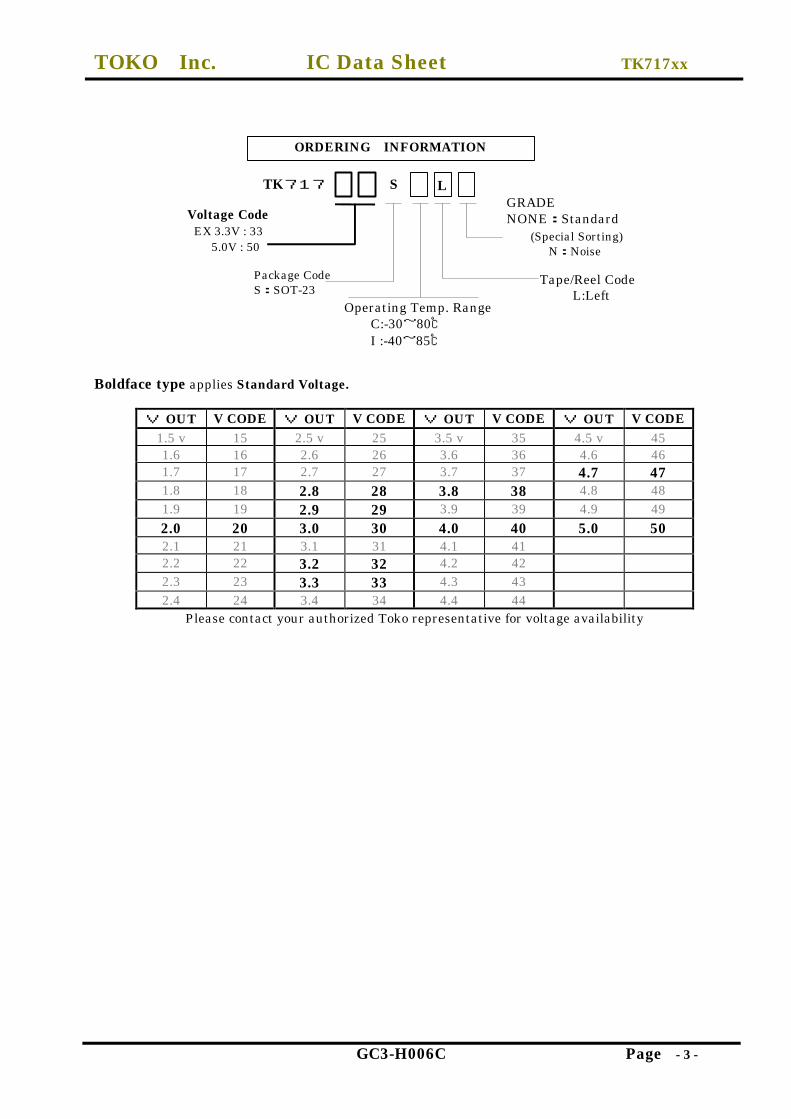
TOKO Inc. IC Data Sheet TK717xx
GC3-H006C Page - 3 -
Boldface type applies Standard Voltage.
V OUT V CODE V OUT V CODE V OUT V CODE V OUT V CODE1.5 v 15 2.5 v 25 3.5 v 35 4.5 v 451.6 16 2.6 26 3.6 36 4.6 461.7 17 2.7 27 3.7 37 4.7 471.8 18 2.8 28 3.8 38 4.8 481.9 19 2.9 29 3.9 39 4.9 492.0 20 3.0 30 4.0 40 5.0 502.1 21 3.1 31 4.1 412.2 22 3.2 32 4.2 422.3 23 3.3 33 4.3 432.4 24 3.4 34 4.4 44
Please contact your authorized Toko representative for voltage availability
Operating Temp. Range C:-30~80℃ I :-40~85℃
Voltage Code EX 3.3V : 33 5.0V : 50
Tape/Reel CodeL:Left
Package CodeS:SOT-23
ORDERING INFORMATION
TK717 SGRADENONE:Standard (Special Sorting) N:Noise
L
TOKO Inc. IC Data Sheet TK717xx
GC3-H006C Page - 4 -
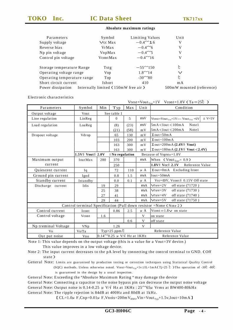
Absolute maximum ratings
Parameters Symbol Limiting Values UnitSupply voltage Vcc Max -0.4~16 VReverse bias VrMax -0.4~6 VNp pin voltage VnpMax -0.4~5 VControl pin voltage VcontMax -0.4~16 V
Storage temperature Range Tstg -55~150 ℃
Operating voltage range Vop 1.8~14 V
Operating temperature range Top -30~80 ℃
Short circuit current Ishort 410 mAPower dissipation Internally limited(150mW free air) 500mW mounted (reference)
Electronic characteristicsVtest=VoutTyp+1V Vcont=1.8V(Ta=25℃)
Parameters Symbol Min Typ Max Unit ConditionOutput voltage Vout See table 1Line regulation LinReg 0 5 mV Vtest=VoutTyp+1V---- VoutTyp +6V ΔV=5V
(8) (23) mV 5mA<Iout<100mA Note1Load regulation LoaReg(21) (58) mV 5mA<Iout<200mA Note1
65 130 mV Iout=50mA103 200 mV Iout=100mA163 300 mV Iout=200mA (2.4V≦Vout)
Vdrop
163 300 mV Iout=180mA (2.1V≦Vout<2.4V)
Dropout voltage
1.5V≦Vout≦2.0V :No regulation Because of VopMin=1.8V
370 mA When (VoutTyp.×0.9)Maximum output current
IoutMax 280
250 1.8V≦Vcc≦2.1V Reference ValueQuiescent current Iq 72 110 μA Iout=0mA Excluding Icont
Ground pin current Ignd 0.8 1.5 mA Iout=50mAStandby current Istandby 0.0 0.1 μA Vcc=8V, Vcont≦0.15V Off state
19 29 mA Vrev=2V off state (71720 )25 38 mA Vrev=3V off state (71730 )27 41 mA Vrev=4V off state (71740 )
Discharge current Idis
29 44 mA Vrev=5V off state (71750 )
Control terminal Specification (Pull down resistor =None(Note 2)Control current Icont 0.86 2.5 μA Vcont=1.8v on state
1.6 V on stateControl voltage Vcont0.6 V off state
Np treminal Voltage VNp 1.26 VVo Vo/Ta Typ=25 ppm/℃ Reference Value
Out put noise Vno 0.14~0.25 μV/√Hz at 1KHz Reference Value
Note 1: This value depends on the output voltage (this is a value for a Vout=3V device.)This value improves in a low voltage device.
Note 2: The input current decreases to the pA level by connecting the control terminal to GND.(Offstate)
General Note: Limits are guaranteed by production testing or correction techniques using Statistical Quality Control
(SQC) methods. Unless otherwise noted. Vtest=VoutTyp+1v;IL=1mA(Tj=25 ℃)The operation of -30℃-80℃
is guaranteed in the design by a usual inspection.
General Note: Exceeding the “Absolute Maximum Rating “ may damage the deviceGeneral Note: Connecting a capacitor to the noise bypass pin can decrease the output noise voltageGeneral Note: Output noise is 0.14-0.25 μV/√Hz at 1KHz : 25~65μVrms at BW400-80kHzGeneral Note: The ripple rejection is 84dB at 400Hz and 80dB at 1kHz.
[CL=1.0μF,Cnp=0.01μF,Vnois=200mVRMS,Vin=VoutTyp+1.5v,Iout=10mA]
TOKO Inc. IC Data Sheet TK717xx
GC3-H006C Page - 5 -
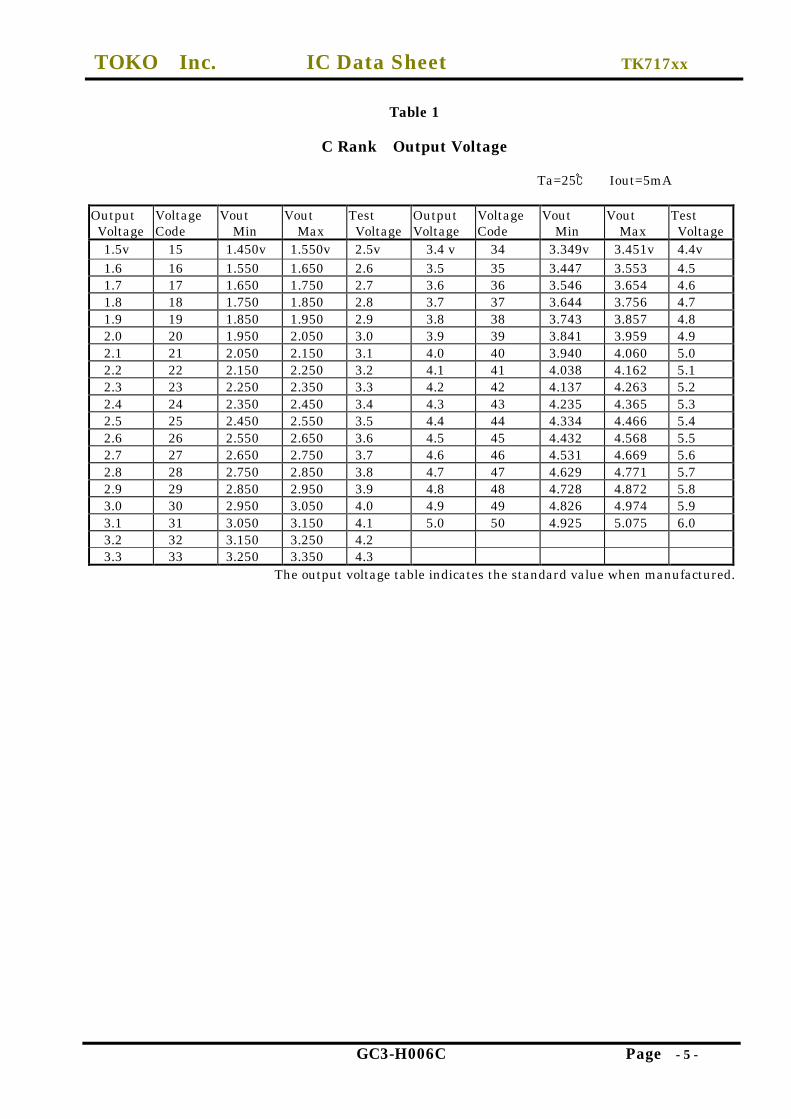
Table 1
C Rank Output Voltage
Ta=25℃ Iout=5mA
Output Voltage
VoltageCode
Vout Min
Vout Max
Test Voltage
OutputVoltage
VoltageCode
Vout Min
Vout Max
Test Voltage
1.5v 15 1.450v 1.550v 2.5v 3.4 v 34 3.349v 3.451v 4.4v 1.6 16 1.550 1.650 2.6 3.5 35 3.447 3.553 4.5 1.7 17 1.650 1.750 2.7 3.6 36 3.546 3.654 4.6 1.8 18 1.750 1.850 2.8 3.7 37 3.644 3.756 4.7 1.9 19 1.850 1.950 2.9 3.8 38 3.743 3.857 4.8 2.0 20 1.950 2.050 3.0 3.9 39 3.841 3.959 4.9 2.1 21 2.050 2.150 3.1 4.0 40 3.940 4.060 5.0 2.2 22 2.150 2.250 3.2 4.1 41 4.038 4.162 5.1 2.3 23 2.250 2.350 3.3 4.2 42 4.137 4.263 5.2 2.4 24 2.350 2.450 3.4 4.3 43 4.235 4.365 5.3 2.5 25 2.450 2.550 3.5 4.4 44 4.334 4.466 5.4 2.6 26 2.550 2.650 3.6 4.5 45 4.432 4.568 5.5 2.7 27 2.650 2.750 3.7 4.6 46 4.531 4.669 5.6 2.8 28 2.750 2.850 3.8 4.7 47 4.629 4.771 5.7 2.9 29 2.850 2.950 3.9 4.8 48 4.728 4.872 5.8 3.0 30 2.950 3.050 4.0 4.9 49 4.826 4.974 5.9 3.1 31 3.050 3.150 4.1 5.0 50 4.925 5.075 6.0 3.2 32 3.150 3.250 4.2 3.3 33 3.250 3.350 4.3
The output voltage table indicates the standard value when manufactured.
TOKO Inc. IC Data Sheet TK717xx
GC3-H006C Page - 6 -
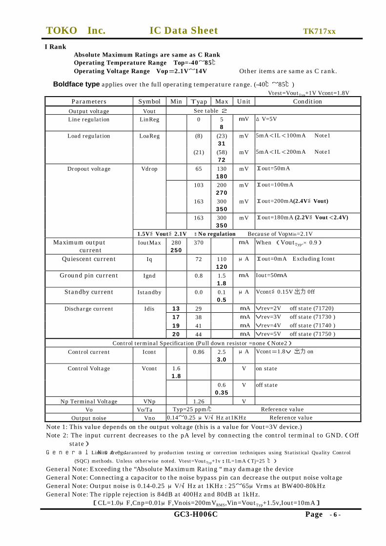
I RankAbsolute Maximum Ratings are same as C RankOperating Temperature Range Top=-40~85℃Operating Voltage Range Vop=2.1V~14V Other items are same as C rank.
Boldface type applies over the full operating temperature range. (-40℃~85℃)Vtest=VoutTyp+1V Vcont=1.8V
Parameters Symbol Min Tyap Max Unit ConditionOutput voltage Vout See table 2Line regulation LinReg 0 5
8mV ΔV=5V
(8) (23)31
mV 5mA<IL<100mA Note1Load regulation LoaReg
(21) (58)72
mV 5mA<IL<200mA Note1
65 130180
mV Iout=50mA
103 200270
mV Iout=100mA
163 300350
mV Iout=200mA(2.4V≦Vout)
Vdrop
163 300350
mV Iout=180mA (2.2V≦Vout<2.4V)
Dropout voltage
1.5V≦Vout≦2.1V :No regulation Because of VopMin=2.1VMaximum output
currentIoutMax 280
250370 mA When (VoutTyp.×0.9)
Quiescent current Iq 72 110120
μA Iout=0mA Excluding Icont
Ground pin current Ignd 0.8 1.51.8
mA Iout=50mA
Standby current Istandby 0.0 0.10.5
μA Vcont≦0.15V 出力 0ff
13 29 mA Vrev=2V off state (71720)
17 38 mA Vrev=3V off state (71730 )
19 41 mA Vrev=4V off state (71740 )
Discharge current Idis
20 44 mA Vrev=5V off state (71750 )
Control terminal Specification (Pull down resistor =none(Note2)Control current Icont 0.86 2.5
3.0μA Vcont=1.8v 出力 on
1.61.8
V on stateControl Voltage Vcont
0.60.35
V off state
Np Terminal Voltage VNp 1.26 VVo Vo/Ta Typ=25 ppm/℃ Reference value
Output noise Vno 0.14~0.25 μV/√Hz at1KHz Reference value
Note 1: This value depends on the output voltage (this is a value for Vout=3V device.)Note 2: The input current decreases to the pA level by connecting the control terminal to GND.(Off
state)General Note: Limits are guaranteed by production testing or correction techniques using Statistical Quality Control
(SQC) methods. Unless otherwise noted. Vtest=VoutTyp+1v;IL=1mA(Tj=25 ℃)
General Note: Exceeding the “Absolute Maximum Rating “ may damage the deviceGeneral Note: Connecting a capacitor to the noise bypass pin can decrease the output noise voltageGeneral Note: Output noise is 0.14-0.25 μV/√Hz at 1KHz : 25~65μVrms at BW400-80kHzGeneral Note: The ripple rejection is 84dB at 400Hz and 80dB at 1kHz.
[CL=1.0μF,Cnp=0.01μF,Vnois=200mVRMS,Vin=VoutTyp+1.5v,Iout=10mA]
TOKO Inc. IC Data Sheet TK717xx
GC3-H006C Page - 7 -
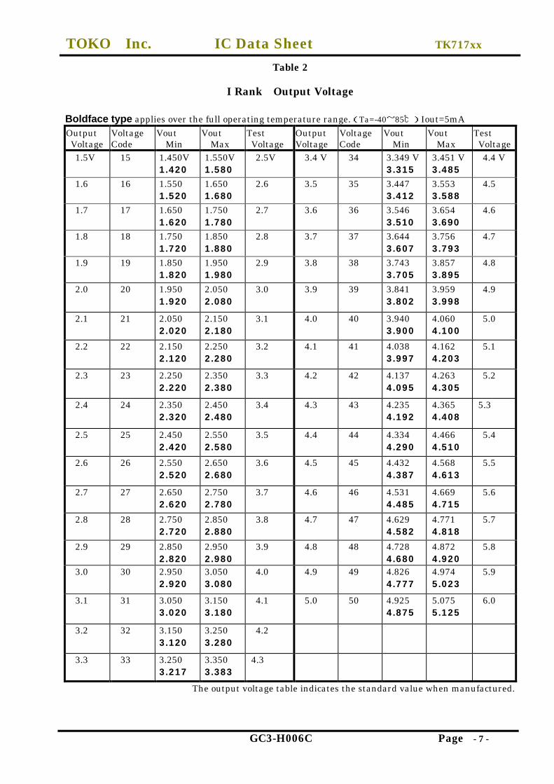
Table 2
I Rank Output Voltage
Boldface type applies over the full operating temperature range.(Ta=-40~85℃)Iout=5mAOutput Voltage
VoltageCode
Vout Min
Vout Max
Test Voltage
OutputVoltage
VoltageCode
Vout Min
Vout Max
Test Voltage
1.5V 15 1.450V1.420
1.550V1.580
2.5V 3.4 V 34 3.349 V3.315
3.451 V3.485
4.4 V
1.6 16 1.5501.520
1.6501.680
2.6 3.5 35 3.4473.412
3.5533.588
4.5
1.7 17 1.6501.620
1.7501.780
2.7 3.6 36 3.5463.510
3.6543.690
4.6
1.8 18 1.7501.720
1.8501.880
2.8 3.7 37 3.6443.607
3.7563.793
4.7
1.9 19 1.8501.820
1.9501.980
2.9 3.8 38 3.7433.705
3.8573.895
4.8
2.0 20 1.9501.920
2.0502.080
3.0 3.9 39 3.8413.802
3.9593.998
4.9
2.1 21 2.0502.020
2.1502.180
3.1 4.0 40 3.9403.900
4.0604.100
5.0
2.2 22 2.1502.120
2.2502.280
3.2 4.1 41 4.0383.997
4.1624.203
5.1
2.3 23 2.2502.220
2.3502.380
3.3 4.2 42 4.1374.095
4.2634.305
5.2
2.4 24 2.3502.320
2.4502.480
3.4 4.3 43 4.2354.192
4.3654.408
5.3
2.5 25 2.4502.420
2.5502.580
3.5 4.4 44 4.3344.290
4.4664.510
5.4
2.6 26 2.5502.520
2.6502.680
3.6 4.5 45 4.4324.387
4.5684.613
5.5
2.7 27 2.6502.620
2.7502.780
3.7 4.6 46 4.5314.485
4.6694.715
5.6
2.8 28 2.7502.720
2.8502.880
3.8 4.7 47 4.6294.582
4.7714.818
5.7
2.9 29 2.8502.820
2.9502.980
3.9 4.8 48 4.7284.680
4.8724.920
5.8
3.0 30 2.9502.920
3.0503.080
4.0 4.9 49 4.8264.777
4.9745.023
5.9
3.1 31 3.0503.020
3.1503.180
4.1 5.0 50 4.9254.875
5.0755.125
6.0
3.2 32 3.1503.120
3.2503.280
4.2
3.3 33 3.2503.217
3.3503.383
4.3
The output voltage table indicates the standard value when manufactured.
TOKO Inc. IC Data Sheet TK717xx
GC3-H006C Page - 8 -
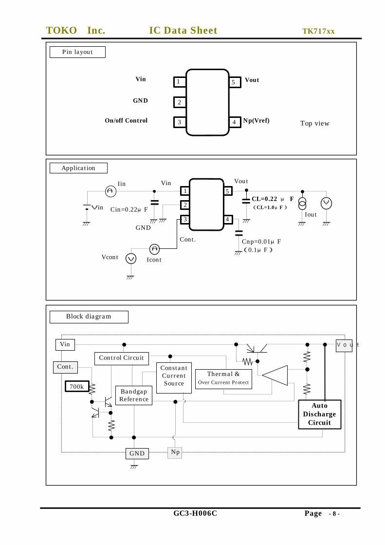
Application
Block diagram
Pin layout
Top view
Vin 1
2
3
5
4
Vout
On/off Control
GND
Np(Vref)
GND
BandgapReference
Cont.
Vin Vout
ConstantCurrentSource
Control Circuit
AutoDischarge
Circuit
Thermal &Over Current Protect
Np
700k
Iin Vout
VCL=0.22 μ F(CL=1.0μF)
Iout
GND
Cont.A
V IcontVcont
AVin
2
3
1 5
4
Cin=0.22μF
Cnp=0.01μF(0.1μF)
Vin
TOKO Inc. IC Data Sheet TK717xx
GC3-H006C Page - 9 -
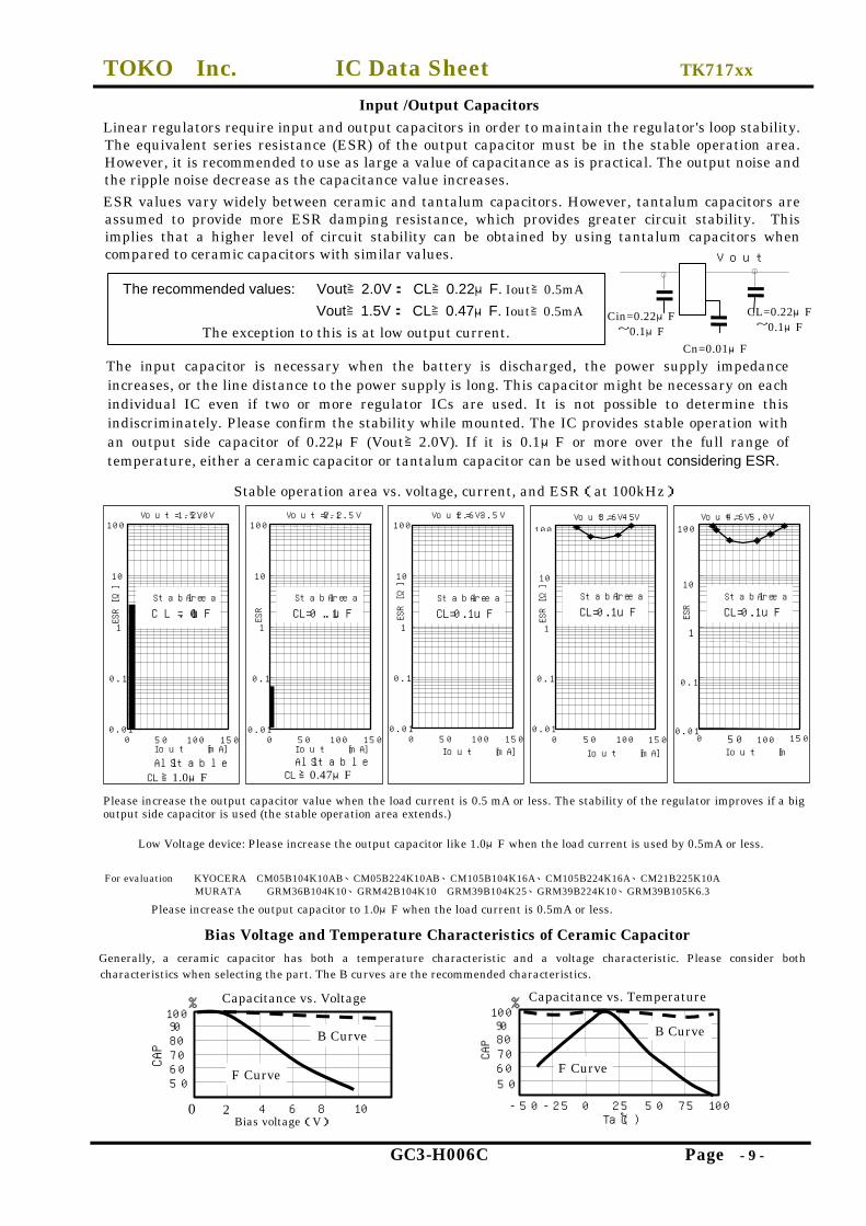
Input /Output CapacitorsLinear regulators require input and output capacitors in order to maintain the regulator's loop stability.The equivalent series resistance (ESR) of the output capacitor must be in the stable operation area.However, it is recommended to use as large a value of capacitance as is practical. The output noise andthe ripple noise decrease as the capacitance value increases.
ESR values vary widely between ceramic and tantalum capacitors. However, tantalum capacitors areassumed to provide more ESR damping resistance, which provides greater circuit stability. Thisimplies that a higher level of circuit stability can be obtained by using tantalum capacitors whencompared to ceramic capacitors with similar values.
The input capacitor is necessary when the battery is discharged, the power supply impedanceincreases, or the line distance to the power supply is long. This capacitor might be necessary on eachindividual IC even if two or more regulator ICs are used. It is not possible to determine thisindiscriminately. Please confirm the stability while mounted. The IC provides stable operation withan output side capacitor of 0.22μF (Vout≧2.0V). If it is 0.1μF or more over the full range oftemperature, either a ceramic capacitor or tantalum capacitor can be used without considering ESR.
Please increase the output capacitor value when the load current is 0.5 mA or less. The stability of the regulator improves if a bigoutput side capacitor is used (the stable operation area extends.)
Low Voltage device: Please increase the output capacitor like 1.0μF when the load current is used by 0.5mA or less.
Please increase the output capacitor to 1.0μF when the load current is 0.5mA or less.
Bias Voltage and Temperature Characteristics of Ceramic CapacitorGenerally, a ceramic capacitor has both a temperature characteristic and a voltage characteristic. Please consider bothcharacteristics when selecting the part. The B curves are the recommended characteristics.
For evaluation KYOCERA CM05B104K10AB、CM05B224K10AB、CM105B104K16A、CM105B224K16A、CM21B225K10AMURATA GRM36B104K10、GRM42B104K10 GRM39B104K25、GRM39B224K10、GRM39B105K6.3
The recommended values: Vout≧2.0V: CL≧0.22μF. Iout≧0.5mA
Vout≧1.5V: CL≧0.47μF. Iout≧0.5mA
The exception to this is at low output current.
0.01
0.1
1
10
100
0 50 100 150
Iout [mA]
ESR
Vout=4.6V-5.0V
Stable Area
CL=0.1uF
Vout=2.6V-3.5V
0.01
0.1
1
10
100
0 50 100 150Iout [mA]
ESR
[Ω
]
Stable Area
CL=0.1uF
150
Vout=1.5V-2.0V
0.01
0.1
1
10
100
0 50 100
ESR
[Ω
]
Iout [mA]
All StableCL≧1.0μF
Stable Area
CL=0.1uF
Vout=2.1V-2.5V
0.01
0.1
1
10
100
0 50 100 150Iout [mA]
All StableCL≧0.47μF
ESR
Stable Area
CL=0..1uF
1500.01
0.1
1
10
100
0 50 100
Iout [mA]
ESR
[Ω
]
Vout=3.6V-4.5V
Stable Area
CL=0.1uF
Stable operation area vs. voltage, current, and ESR(at 100kHz)
% Capacitance vs. Voltage
0Bias voltage(V)
CA
P
2 4 6 8 10
5060708090100
B Curve
F Curve
Capacitance vs. Temperature%
6050
8090
100
70CA
P
-50 -25 0 25 50 75 100Ta(℃)
B Curve
F Curve
Vout
Cn=0.01μF
CL=0.22μF~0.1μF
Cin=0.22μF~0.1μF
TOKO Inc. IC Data Sheet TK717xx
GC3-H006C Page - 10 -
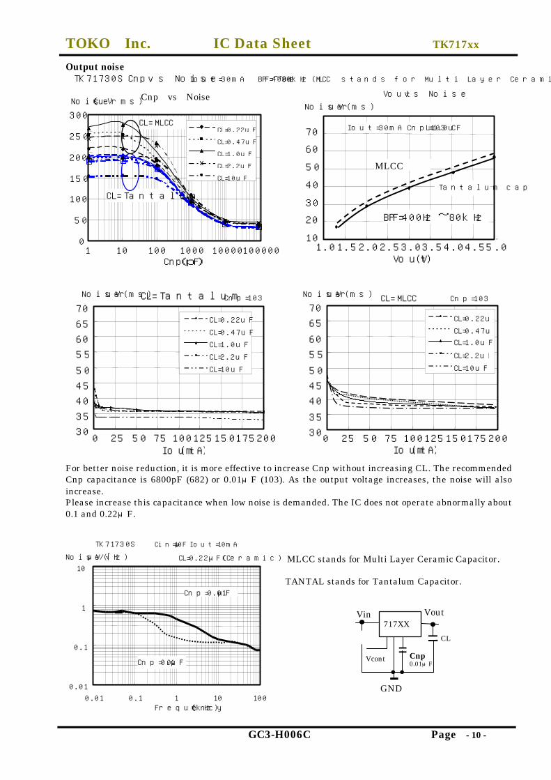
Output noise
For better noise reduction, it is more effective to increase Cnp without increasing CL. The recommendedCnp capacitance is 6800pF (682) or 0.01μF (103). As the output voltage increases, the noise will alsoincrease.Please increase this capacitance when low noise is demanded. The IC does not operate abnormally about0.1 and 0.22μF.
MLCC stands for Multi Layer Ceramic Capacitor.
TANTAL stands for Tantalum Capacitor.
TK71730S Cnp vs Noise Iout=30mA BPF=400Hz~80kHz (MLCC stands for Multi Layer Ceramic Capacitor)
30
35
40
45
50
55
60
65
70
0 25 50 75 100 125 150 175 200Iout(mA)
Noise(uVrms)
CL=0.22uF
CL=0.47uF
CL=1.0uF
CL=2.2uF
CL=10uF
CL=Tantalum Cnp=103
TK71730S Cin=10μF Iout=10mA
0.01
0.1
1
10
0.01 0.1 1 10 100Frequency(kHz)
Noise(μV/√Hz) CL=0.22μF(Ceramic)
Cnp=0.01μF
Cnp=0.10μF
Vout vs Noise
10
20
30
40
50
60
70
1.0 1.5 2.0 2.5 3.0 3.5 4.0 4.5 5.0Vout(V)
Noise(uVrms)
Iout=30mA Cnp=103 CL=1.0uF
BPF=400Hz~80kHz
30
35
40
45
50
55
60
65
70
0 25 50 75 100 125 150 175 200Iout(mA)
Noise(uVrms)
CL=0.22uF
CL=0.47uF
CL=1.0uF
CL=2.2uF
CL=10uF
CL=MLCC Cnp=103
Tantalum cap
MLCC
Cnp(pF)
0
50
100
150
200
250
300
1 10 100 1000 10000 100000
Noise(uVrms)
CL=Tantalum
CL=MLCCCL=0.22uF
CL=0.47uF
CL=1.0uF
CL=2.2uF
CL=10uF
Cnp vs Noise
CL
GND
717XXVoutVin
Cnp0.01μF
Vcont
TOKO Inc. IC Data Sheet TK717xx
GC3-H006C Page - 11 -
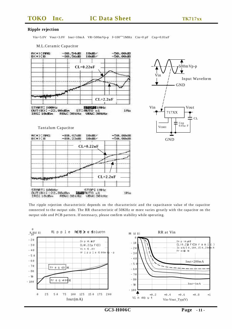
Ripple rejection
The ripple rejection characteristic depends on the characteristic and the capacitance value of the capacitorconnected to the output side. The RR characteristic of 50KHz or more varies greatly with the capacitor on theoutput side and PCB pattern. If necessary, please confirm stability while operating.
-100
-90
-80
-70
-60
-50
-40
-30
-20
-10
0 Ripple Rejection(RR) vs Iout
0 25 50 75 100 125 150 175 200
Iout(mA)
R.R(dB)
Cnp=0.01μF
CL=0.22μF(C)Vin=5.0V
Vripple=500mVp-p
Freq=1kHz
Freq=400Hz
RR at Vin
-100
-90
-80
-70
-60
-50
-40
-30
-20
-10
0
+0.2 +0.4 +0.6 +0.8 +1
Vin-Vout_Typ(V)
RR (dB)
Cnp:0.01μFCL:0.22μF(Ceramic)Iout:1,50,100,150,200mAFreq:1kHz
Iout=1mA
Iout=200mA
Vin=Vout
Vin=5.0V Vout=3.0V Iout=10mA VR=500mVp-p f=100~1MHz Cin=0 pF Cnp=0.01uF
CL=0.22uF
CL=2.2uF
CL=0.22uF
CL=2.2uF
Tantalum Capacitor
M.L.Ceramic Capacitor
CL
GND
717XXVoutVin
Cnp0.01μFVcont
Vin
500mVp-p
GND
Input Waveform
TOKO Inc. IC Data Sheet TK717xx
GC3-H006C Page - 12 -
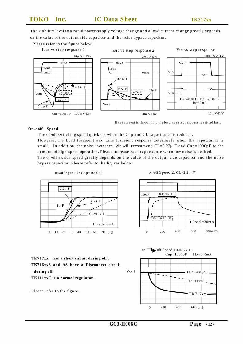
The stability level to a rapid power-supply voltage change and a load current change greatly depends
on the value of the output side capacitor and the noise bypass capacitor.
Please refer to the figure below.
On/off SpeedThe on/off switching speed quickens when the Cnp and CL capacitance is reduced.However, the Load transient and Line transient response deteriorate when the capacitance issmall. In addition, the noise increases. We will recommend CL=0.22μF and Cnp=1000pF to thedemand of high-speed operation. Please increase each capacitance when low noise is desired.The on/off switch speed greatly depends on the value of the output side capacitor and the noisebypass capacitor. Please refer to the figures below.
TK717xx has a short circuit during off .
TK716xxS and AS have a Disconnect circuit
during off.
TK111xxC is a normal regulator.
Please refer to the figure.
Vin
Vout
Vcc vs step response
500μS/Div
Vo+1
Cnp=0.001μF,CL=1.0μFIo=30mA
10mV/DiV
Vo+2
0 200 600400 μS
TK716xxS,AS
TK111xxC
TK717xx
on off Speed: CL=2.2μF、 Cnp=1000pF I Load=0mA
Vout
If the current is thrown into the load, the step response is settled fast.
Cnp=0.001μF 100mV/Div
Iout vs step response 2
2mS/Div
Iout
Vout
20mV/Div
10μF4.7μF
2.2μF
CL=1μF
30mA
0mA
Iout vs step response 1
10μS/Div
0mA
30mA
10μF
CL=1μF
2.2μF
4.7μF
Iout
Vout
on/off Speed 2: CL=2.2μF
0 800μS200 400 600
ILoad =30mACnp=0.01μF
100pF 0.001μF
0 10 5020 6030 7040 μS
I Load=30mA
CL=10μF
4.7μF
2.2μF
1μF
on/off Speed 1: Cnp=1000pF
TOKO Inc. IC Data Sheet TK717xx
GC3-H006C Page - 13 -
Dropout voltage
-350
-300
-250
-200
-150
-100
-50
0
0 50 100 150 200 250 300Iout (mA)
Vdrop(mV)
△Vin(mV)
Vin vs Vout
-180
-160
-140
-120
-100
-80
-60
-40
-20
0
20
-100 0 100 200 300
△Vout(mV)Iout=0~250mA
Iout=50mA Step
Vout(V)Short Circuit current
0.0
1.0
2.0
3.0
4.0
5.0
0 100 200 300 400 500Iout (mA) Vop(V)
IoutMax(mA)
100
150
200
250
300
350
400
1.7 1.8 1.9 2 2.1 2.2 2.3 2.4
IoutMax at low VopTK71715 ∼ TK71724
Line regulation
-35
-30
-25
-20
-15
-10
-5
0
5
10
15
0 5 10 15 20
Vin(V)
△Vout(mV)
Vo1.5V
Vo2.0V
Vo3.0V
Vo4.0V
Vo5.0V
Vo=2.0V
Vo=5.0V
△Vout(mV) Load regulation
-40-35-30-25-20-15-10-505
10
0 50 100 150 200
Iout (mA)
Vo=3.0V
TOKO Inc. IC Data Sheet TK717xx
GC3-H006C Page - 14 -
0.0
0.2
0.4
0.6
0.8
1.0
1.2
1.4
1.6
1.8
0 1 2 3 4 5 6 7 8 9 10Vin(V)
Iin(mA)
Vo2.0V
Vo3.0V
Vo4.0V
Vo5.0V
Icc at Low voltage Io=0mA
GND pin Current
0123456789
10
0 50 100 150 200Iout (mA)
Ignd(mA)
Discharge Current
0
10
20
30
40
50
60
0.0 1.0 2.0 3.0 4.0 5.0
Vout(V)
Idis(mA) Standby Current
1.0E-12
1.0E-11
1.0E-10
1.0E-09
1.0E-08
1.0E-07
1.0E-06
0 5 10 15 20Vin(V)
Is(A)
Control Current Io=0mA
0.0
0.5
1.0
1.5
2.0
2.5
3.0
3.5
4.0
4.5
0 1 2 3 4
Vcont(V)
Icont(uA)
Icont
Vout
TOKO Inc. IC Data Sheet TK717xx
GC3-H006C Page - 15 -
Temperature characteristics-1 (Ta: Ambient temperature)
0.6
0.8
1.0
1.2
1.4
1.6
-50 -25 0 25 50 75 100Ta(℃)
Vcont(ONpoint)
Vcont(OFFpoint)
on/off Point VoltageVcont(V)
0.00.51.01.52.02.53.03.54.04.55.0
-50 -25 0 25 50 75 100Ta(℃)
Vcont=1.8/2.0/3.0/4.0V
Control currentIcont(uA)
Vcont=1.8V
Vcont=4.0V
Iout Max(mA) Iout MAX
200
250
300
350
400
450
500
-50 -25 0 25 50 75 100Ta(℃)
Vout=(VoutTyp.×0.9)
Dropout voltage
0
50
100
150
200
250
300
-50 -25 0 25 50 75 100
Ta(℃)
Iout=30/50/100/150/200/250/280mAVdrop(mV)
Io=150mA
Io=100mA
Io=50mA
Io=200mA
Io=30mA
0.0
1.0
2.0
3.0
4.0
5.0
6.0
7.0
8.0
-50 -25 0 25 50 75 100Ta(℃)
Iout=30/60/100/150/200mA
GND pin currentIgnd(mA)
Io=150mA
Io=100mA
Io=60mA
Io=200mA
Io=30mA
Io=280mAIo=250mA
Discharge current
05
1015
202530
3540
4550
-50 -25 0 25 50 75 100Ta(℃)
Idis (mA)
Vrev=3.0V
Vrev=2.0V
TOKO Inc. IC Data Sheet TK717xx
GC3-H006C Page - 16 -
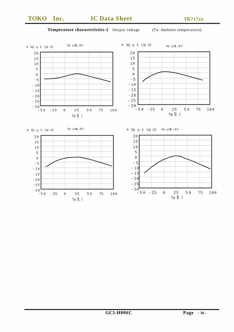
Temperature characteristics-2 Output voltage (Ta: Ambient temperature)
-30
-25
-20
-15
-10
-5
0
5
10
15
20
-50 -25 0 25 50 75 100
Ta(℃)
△Vout(mV) Vout=4.0V
-30-25
-20-15-10-5
05
10
1520
-50 -25 0 25 50 75 100Ta(℃)
△Vout(mV) Vout=5.0V
-30
-25
-20
-15
-10
-5
0
5
10
15
20
-50 -25 0 25 50 75 100
Ta(℃)
△Vout(mV) Vout=2.0V
-30-25-20
-15-10-505
101520
-50 -25 0 25 50 75 100Ta(℃)
△Vout(mV) Vout=3.0V
TOKO Inc. IC Data Sheet TK717xx
GC3-H006C Page - 17 -
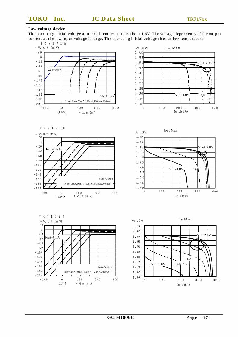
Low voltage deviceThe operating initial voltage at normal temperature is about 1.6V. The voltage dependency of the outputcurrent at the low input voltage is large. The operating initial voltage rises at low temperature.
TK71715
(1.5V)-100 0 100 200 300
△Vin(mV)
-200
-180-160
-140
-120
-100-80
-60
-40
-200
20
△Vout(mV)
50mA Step
Iout=0mA,50mA,100mA,150mA,200mA
Iout=0mA
-200
-180
-160
-140
-120
-100
-80
-60
-40
-20
0
20
(1.8V)-100 0 100 200 300
△Vin(mV)
△Vout(mV)
TK71718
Iout=0mA
50mA Step
Iout=0mA,50mA,100mA,150mA,200mA
1.40
1.45
1.50
1.55
1.60
1.65
1.70
1.75
1.80
1.85
1.90
0 100 200 300 400
Iout(mA)
Vout(V)Iout Max
Vin≧2.0V
Vin=1.8V 1.9V
Iout MAX
1.10
1.15
1.20
1.25
1.30
1.35
1.40
1.45
1.50
1.55
1.60
0 100 200 300 400Iout(mA)
Vout(V)
Vin=1.8V 1.9V
Vin≧2.0V
-200
-180
-160
-140
-120
-100
-80
-60
-40
-200
20
-100 0 100 200 300(2.0V) △Vin(mV)
△Vout(mV)
TK71720
Iout=0mA
50mA Step
Iout=0mA,50mA,100mA,150mA,200mA
1.60
1.65
1.70
1.75
1.80
1.85
1.90
1.95
2.00
2.05
2.10
0 100 200 300 400
Iout(mA)
Vout(V) Iout Max
Vin≧2.1V
Vin=1.8V 1.9V
2.0V
TOKO Inc. IC Data Sheet TK717xx
GC3-H006C Page - 18 -
Layout Material:Grass epoxy 20×20mm t=0.8mm
Pd=500 mW when mounted as recommended. Derate at 4.0 mW/°C for operation above 25°C. Thethermal resistance is (θja=250℃/W). The heat loss of A and B are done in total. The package loss islimited at the temperature that the internal temperature sensor works (about 150℃). Therefore, thepackage loss is assumed to be an internal limitation. There is no heat radiation characteristic of thepackage unit assumed because of the small size. Heat is carried away by the device being installed on thePCB. This value changes by the material and the copper pattern etc. of the PCB. Enduring losses ofabout 500mW becomes possible in a lot of applications operating at 25℃.
Determining the thermal resistance when mounted on a PCB.The operating chip junction temperature is shown byTj=θja×Pd+Ta. Tj of IC is set to about 150℃.Pd is a value when the overtemperature sensor is made to work.
Pd is easily obtained.Mount the IC on the print circuit board. Short between the output pin and ground. after that, raise inputvoltage from 0V to evaluated voltage (see*1) gradually.At shorted the output pin, the power dissipation PD can be expressed as Pd=Vin × Iin.The input current decreases gradually as the temperature of the chip becomes high. After a while, itreaches the thermal equilibrium. Use this currrent value at the thermal equilibrium. In almost all thecases, it shows 500mW(SOT23-5) or more.
*1 In the case that the power, Vin × Ishort(Short Circuit Current), becomes more than twice of the maximum rating of its
power dissipation in a moment, there is a possibility that the IC is destroyed before internal thermal protection works.
Pd is obtained by the normal temperature degrees. The current that can be used at the highest operatingtemperature is obtained from the graph of the figure below.
Procedure (Do when PCB mounted).1. Pd is obtained (Vin×Iin when the output side is short-circuited).2. Pd is plotted on the horizontal line to 25℃.3. Pd is connected with the point of 150℃ by the straight line
(bold face line).4. A line is extended vertically above the point of the use temperature in the
design. For instance, 75℃ is assumed (broken line).
5. Extend the intersection of the derating curve (fat solid line) and (brokenline) to the left and read the Pd value.
6.DPd÷(Vinmax―Vout)=Iout (at 75℃)
The maximum current that can be used at the highest operating temperature is:Iout≒ DPd÷(Vinmax―Vout).When (Vinmax―Vout) is small, a lot of Iout is calculated. However, use that exceeds IoutMax cannotbe done.
TK
717
xx
Vin
on/off
GND
N.pass
Vout
Ta(Ta=25℃)
150=θja×pd+25
θja×Pd=125
θja=(125/pd)(℃/mW)
Pd(mW)
25 50 100 150℃0 (75)
DPd
Pd2
3
4
5
25 50 100 150℃0
Pd(mW)
(85)
500-4.0mW/℃
Free Air
0
Mounted
TOKO Inc. IC Data Sheet TK717xx
GC3-H006C Page - 19 -
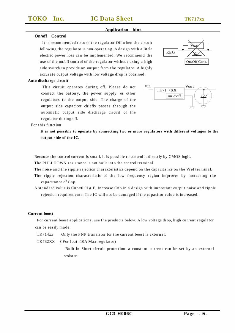
Application hintOn/off Control
It is recommended to turn the regulator Off when the circuit
following the regulator is non-operating. A design with a little
electric power loss can be implemented. We recommend the
use of the on/off control of the regulator without using a high
side switch to provide an output from the regulator. A highly
accurate output voltage with low voltage drop is obtained.
Auto discharge circuit
This circuit operates during off. Please do not
connect the battery, the power supply, or other
regulators to the output side. The charge of the
output side capacitor chiefly passes through the
automatic output side discharge circuit of the
regulator during off.
For this function
It is not possible to operate by connecting two or more regulators with different voltages to the
output side of the IC.
Because the control current is small, it is possible to control it directly by CMOS logic.
The PULLDOWN resistance is not built into the control terminal.
The noise and the ripple rejection characteristics depend on the capacitance on the Vref terminal.
The ripple rejection characteristic of the low frequency region improves by increasing the
capacitance of Cnp.
A standard value is Cnp=0.01μF. Increase Cnp in a design with important output noise and ripple
rejection requirements. The IC will not be damaged if the capacitor value is increased.
Current boost
For current boost applications, use the products below. A low voltage drop, high current regulator
can be easily made.
TK714xx Only the PNP transistor for the current boost is external.
TK732XX (For Iout=10A Max regulator)
Built-in Short circuit protection: a constant current can be set by an external
resistor.
TK717XXon/off
VoutVin
REG
VsatOP
On/Off Cont.
TOKO Inc. IC Data Sheet TK717xx
GC3-H006C Page - 20 -
Definition of TermsThe output voltage tables are specified with a test voltage of Vin = output voltage Typ+1V.
Output Voltage (Vout)The output voltage is specified with Vin = output voltage Typ+1V and output current (Iout=5mA).
Maximum Output Current (Iout Max) The output current is measured when the output voltage decreases to(VoutTyp.×0.9). The input
voltage is (output voltage Typ+1V). The maximum output current is measured in a short timeso that it is not influenced by the temperature of the chip.
The output current decreases during low voltage operation.Please refer to the "Low input voltage-output current" graph for 2.1V or less.
Dropout Voltage (Vdrop)The dropout voltage is the difference between the input voltage and the output voltage at which
point the regulator starts to fall out of regulation. Below this value, the output voltage will fallas the input voltage is reduced. It is dependent upon the load current (Iout) and the junctiontemperature (Tj).
The input voltage is gradually decreased below the test voltage. It is the voltage difference betweenthe input and the output when the output voltage decreases by 100mV.
Line Regulation(Lin Reg)Line regulation is the ability of the regulator to maintain a constant output voltage as the input
voltage changes. The line regulation is specified as the input voltage is changed from (outputvoltage Typ+1V) to (output voltage Typ+6V). This measurement is not influenced by thetemperature of the IC and is measured in a short time.
Load Regulation(Load Reg)Load regulation is the ability of the regulator to maintain a constant output voltage as the load current
changes. The input voltage is set to (output voltage Typ+1V). The output voltage change ismeasured as the load current changes from 5 to 100mA and from 5 to 200mA. This measurementis not influenced by the temperature of the IC and is measured in a short time.
Quiescent Current (Iq)The quiescent current is the current which flows through the ground terminal under no load
conditions (Io=0 mA).
Ground Pin Current(Ignd)Ground pin current is the current which flows through the GND terminal according to load current.
It is measured by (input current-output current).
Ripple Rejection(RR)Ripple rejection is the ability of the regulator to attenuate the ripple content of the input voltage at
the output. It is specified with the input voltage =(Vout+1.5V), Io=10mA, CL=1.0μF andCN=0.01μF. An Alternating Current source of (f=1Khz and 200mVRMS) is superimposed to thepower-supply voltage. Ripple rejection is the ratio of the ripple content of the output vs. theinput and is expressed in dB. It is typically about 80dB at 1kHz. The ripple rejection improveswhen the value of the capacitor at the noise bypass terminal in the circuit is large. However,the on/off response worsens.
TOKO Inc. IC Data Sheet TK717xx
GC3-H006C Page - 21 -
Standby CurrentStandby current is the current which flows into the regulator when the control voltage is made 0
volts. It is measured with an input voltage of 8V.
PROTECTION CIRCUITS
Short circuit SensorThis sensor operates when there is excessive output current. The short circuit sensor protects the
device if the output is accidentally shorted to GND. The current flows at the set peak value.
Thermal Sensor The thermal sensor protects the device if the junction temperature exceeds the safe value (Tj = 150
°C). This temperature rise can be caused by extreme heat, excessive power dissipation causedby large output voltage drops, or excessive output current. The regulator will shut off when thetemperature exceeds the safe value. As the junction temperature decreases, the regulator willbegin to operate again. Under sustained fault conditions, the regulator output will oscillate asthe device turns off then resets. Please improve heat radiation or lower the input electricpower. When heat radiation is poor, the forecast package loss is not obtained.
* In the case that the power, Vin × Ishort(Short Circuit Current), becomes more than twice of the maximum rating of its
power dissipation in a moment, there is a possibility that the IC is destroyed before internal thermal protection works.
ESD MM 200pF 0Ω 200V Min
HBM 100pF 1.5kΩ 2000V Min
TOKO Inc. IC Data Sheet TK717xx
GC3-H006C Page - 22 -
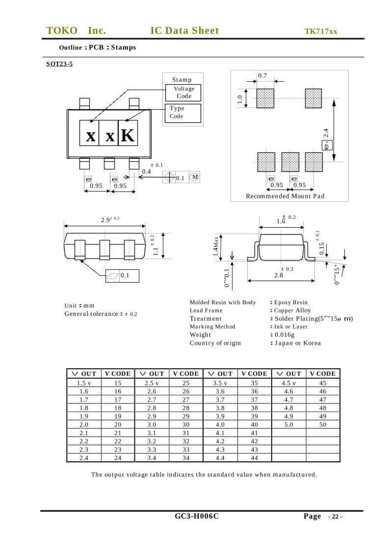
Outline;PCB;Stamps
SOT23-5
V OUT V CODE V OUT V CODE V OUT V CODE V OUT V CODE1.5 v 15 2.5 v 25 3.5 v 35 4.5 v 451.6 16 2.6 26 3.6 36 4.6 461.7 17 2.7 27 3.7 37 4.7 471.8 18 2.8 28 3.8 38 4.8 481.9 19 2.9 29 3.9 39 4.9 492.0 20 3.0 30 4.0 40 5.0 502.1 21 3.1 31 4.1 412.2 22 3.2 32 4.2 422.3 23 3.3 33 4.3 432.4 24 3.4 34 4.4 44
The output voltage table indicates the standard value when manufactured.
Recommended Mount Pad
0.950.95
1.0
0.7
2.4
e e
e1
Unit:mmGeneral tolerance:±0.2
2.9±0.2
1.1
±0.
2
0.1
x x K
0.4
0.95 0.95
TypeCode
VoltageCode
e e
±0.1
0.1 M
Stamp
Molded Resin with Body :Epoxy ResinLead Frame :Copper AlloyTreatment :Solder Plating(5~15μm)Marking Method :Ink or LaserWeight :0.016gCountry of origin :Japan or Korea
1.4M
ax
0.15
±0.
1
0~0.
1
2.8±0.3
±0.21.6
0~15
°
TOKO Inc. IC Data Sheet TK717xx
GC3-H006C Page - 23 -
NOTEPlease be sure that you carefully discuss your planned purchase with our office if you intend to use theproducts in this data sheet under conditions where particularly extreme standards of reliability arerequired, or if you intend to use products for applications other than those listed in this data sheet.l Power drive products for automobile, ship or aircraft transport systems; steering and navigationsystems, emergency signal communications systems, and any system other than those mentionedabove which include electronic sensors, measuring, or display devices, and which could cause majordamage to life, limb or property if misused or failure to function.l Medical devices for measuring blood pressure, pulse, etc., treatment units such as coronarypacemakers and heat treatment units, and devices such as artificial organs and artificial limb systemswhich augment physiological functions.l Electrical instruments, equipment or systems used in disaster or crime prevention.
n Semiconductors, by nature, may fail or malfunction in spite of our devotion to improve product qualityand reliability. We urge you to take every possible precaution against physical injuries, fire or otherdamages which may cause failure of our semiconductor products by taking appropriate measures,including a reasonable safety margin, malfunction preventive practices and fire-proofing whendesigning your products.
n This data sheet is effective from Oct. 2002. Note that the contents are subject to change ordiscontinuation without notice. When placing orders, please confirm specifications and deliverycondition in writing.
n TOKO is not responsible for any problems nor for any infringement of third party patents or any otherintellectual property rights that may arise from the use or method of use of the products listed in thisdata sheet. Moreover, this data sheet does not signify that TOKO agrees implicitly or explicitly tolicense any patent rights or other intellectual property rights which it holds.
n None of ozone depleting substances(ODS) under the Montreal Protocol is used in manufacturingprocess of us.
If you need more information on this product and other TOKO products, please contact us.
OFFICE n TOKO Inc. Headquarters1-17, Higashi-yukigaya 2-chome, Ohta-ku, Tokyo,145-8585, Japan
TEL: +81.3.3727.1161FAX: +81.3.3727.1176 or +81.3.3727.1169Web site: http://www.toko.co.jp/
n TOKO AmericaWeb site: http://www.toko.com/n TOKO EuropeWeb site: http://www.tokoeurope.com/n TOKO Hong KongWeb site: http://www.toko.com.hk/n TOKO TaiwanWeb site: http://www.tokohc.com.tw/
n TOKO SingaporeWeb site: http://www.toko.com.sg/n TOKO SeoulWeb site: http://www.toko.co.kr/n TOKO ManilaWeb site: http://www.toko.com.ph/n TOKO BrazilWeb site: http://www.toko.com.br/
YOUR DISTRIBUTORMEETING YOUR NEEDS
TO BUILD THE QUALITY RELIED BY COSTOMERS