
High-ResolutionMulti-BitIncrementalConverter with1.5...
4
High-Resolution Multi-Bit Incremental Converter with 1.5-μV Residual Offset and 94-dB SFDR Andrea Agnes, Edoardo Bonizzoni (University of Pavia, Department of Electronics, Pavia - ITALY) Alessandro D’Amato, Ivano Galdi (National Semiconductor, Rozzano (MI) - ITALY) Franco Maloberti (University of Pavia, Department of Electronics, Pavia - ITALY) Abstract This paper presents an incremental converter, based on a second order scheme, able to achieve 19 bit of resolution with 512 clock periods. The design avoids an initial error by an optimal reset of the two integrators, uses a 3-bit quantizer that enhances the resolution, and cancels the offset with a novel technique based on single or double chopping. The circuit, fabricated in a mixed 0.18-0.6 μm CMOS technology, obtains 1.5-μV residual offset with 2VPP fully differential range. Key words: CMOS analog integrated circuits, Sigma-Delta modulation, analog-to-digital conversion 1. Introduction Incremental converters are used for low conversion rate and high resolution. The typical application is for sensors and instrumentations that require low offset and high dy- namic range, (1) . Having a large number of bit in the data converter relaxes the gain requirement of the pre-amplifier, but makes more important the request of having very low offset in the data converter. The equivalent number of bit of an incremental converter with single-bit quantizer depends on the order of the mod- ulator, the digital post processing and the number of clock cycles. When the order of the modulator is higher than 2, the request of ensuring stability limits the effectiveness of the architecture. Supposing to use as post processing the cascade of a number of accumulators equal to the order of the scheme, with N clock cycles the converter achieves log2N bit for a first order, log2(N (N − 1)) for a second order, and log2(αN (N − 1)(N − 2)) for a third order, where α can be as low as 1/32, (2) . Therefore, the benefit of a third order scheme is significantly reduced. The use of multi-bit quan- tizers is not suitable for incremental architectures because the mismatch between unity elements can not be effectively corrected by the noise shaping methods, as done in ΣΔ mod- ulators. The incremental converter is a Nyquist-rate archi- tecture that does not benefit much from spectral shaping obtained within the N conversion cycles. This paper obtains 19 bit and virtually zero offset using a second order incremental scheme with N =512. Three main innovations favor the result. They are: the use of a 3-bit quantizer with inherent linearity, an optimal reset of the in- tegrators to avoid a major error at the first clock period, a single or double chopping that cancels the offset. 2. Conventional Architectures and Features An incremental converter is a ΣΔ modulator with initial reset of integrators. For high order architectures, it is nec- essary to use single stage schemes because MASH solutions are not able to generate the analog quantization error with enough precision. Moreover, the mismatch between unity elements prevents the use of multi-bit quantizers. The use of single-bit quantizers in ΣΔ modulators grants an intrinsic linearity, but the input of the first integrator is wide. The output swing of the integrators is also large because the quantization error is half of the converter refer- ence voltage, VRef . The latter problem is fixed by a suitable choice of the supply voltage, VDD, and VRef . In order to avoid op-amps saturation, VRef is a small fraction of VDD. More important is the large signal at the input differential stages that causes slewing. The issue is analyzed referring to the scheme of Fig. 1, a single-bit second order incremental converter with input feedforward. The injecting network is made by an input switched capacitor that injects its signal on the first integrator. Immediately after the switching of Φ1, capacitors C1, C2, and C3 (the equivalent amplifier output capacitance) determine the input differential voltage, Vd. It is Vd = VinC1/(C1 + Ceq ), where Ceq is the series connection Fig. 1. Single-bit second order incremental converter scheme. 1/4 The 2010 IEEJ International Workshop on AVLSI, Pavia, Italy 103
Transcript of High-ResolutionMulti-BitIncrementalConverter with1.5...
High-Resolution Multi-Bit Incremental Converter
with 1.5-μV Residual Offset and 94-dB SFDR
Andrea Agnes, Edoardo Bonizzoni (University of Pavia, Department of Electronics, Pavia - ITALY)
Alessandro D’Amato, Ivano Galdi (National Semiconductor, Rozzano (MI) - ITALY)
Franco Maloberti (University of Pavia, Department of Electronics, Pavia - ITALY)
Abstract
This paper presents an incremental converter, based on a second order scheme, able to achieve 19 bit of resolution with
512 clock periods. The design avoids an initial error by an optimal reset of the two integrators, uses a 3-bit quantizer
that enhances the resolution, and cancels the offset with a novel technique based on single or double chopping. The
circuit, fabricated in a mixed 0.18-0.6 μm CMOS technology, obtains 1.5-μV residual offset with 2VPP fully differential
range.
Key words: CMOS analog integrated circuits, Sigma-Delta modulation, analog-to-digital conversion
1. Introduction
Incremental converters are used for low conversion rate
and high resolution. The typical application is for sensors
and instrumentations that require low offset and high dy-
namic range, (1). Having a large number of bit in the data
converter relaxes the gain requirement of the pre-amplifier,
but makes more important the request of having very low
offset in the data converter.
The equivalent number of bit of an incremental converter
with single-bit quantizer depends on the order of the mod-
ulator, the digital post processing and the number of clock
cycles. When the order of the modulator is higher than 2,
the request of ensuring stability limits the effectiveness of
the architecture. Supposing to use as post processing the
cascade of a number of accumulators equal to the order of
the scheme, with N clock cycles the converter achieves log2N
bit for a first order, log2(N(N − 1)) for a second order, and
log2(αN(N − 1)(N − 2)) for a third order, where α can be
as low as 1/32, (2). Therefore, the benefit of a third order
scheme is significantly reduced. The use of multi-bit quan-
tizers is not suitable for incremental architectures because
the mismatch between unity elements can not be effectively
corrected by the noise shaping methods, as done in ΣΔ mod-
ulators. The incremental converter is a Nyquist-rate archi-
tecture that does not benefit much from spectral shaping
obtained within the N conversion cycles.
This paper obtains 19 bit and virtually zero offset using a
second order incremental scheme with N=512. Three main
innovations favor the result. They are: the use of a 3-bit
quantizer with inherent linearity, an optimal reset of the in-
tegrators to avoid a major error at the first clock period, a
single or double chopping that cancels the offset.
2. Conventional Architectures and Features
An incremental converter is a ΣΔ modulator with initial
reset of integrators. For high order architectures, it is nec-
essary to use single stage schemes because MASH solutions
are not able to generate the analog quantization error with
enough precision. Moreover, the mismatch between unity
elements prevents the use of multi-bit quantizers.
The use of single-bit quantizers in ΣΔ modulators grants
an intrinsic linearity, but the input of the first integrator
is wide. The output swing of the integrators is also large
because the quantization error is half of the converter refer-
ence voltage, VRef . The latter problem is fixed by a suitable
choice of the supply voltage, VDD, and VRef . In order to
avoid op-amps saturation, VRef is a small fraction of VDD.
More important is the large signal at the input differential
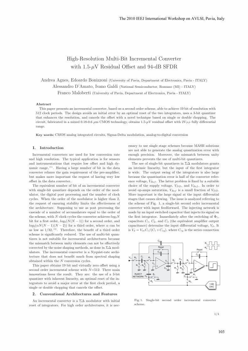
stages that causes slewing. The issue is analyzed referring to
the scheme of Fig. 1, a single-bit second order incremental
converter with input feedforward. The injecting network is
made by an input switched capacitor that injects its signal on
the first integrator. Immediately after the switching of Φ1,
capacitors C1, C2, and C3 (the equivalent amplifier output
capacitance) determine the input differential voltage, Vd. It
is Vd = VinC1/(C1+Ceq), where Ceq is the series connection
Fig. 1. Single-bit second order incremental converter
scheme.
1/4
The 2010 IEEJ International Workshop on AVLSI, Pavia, Italy
103
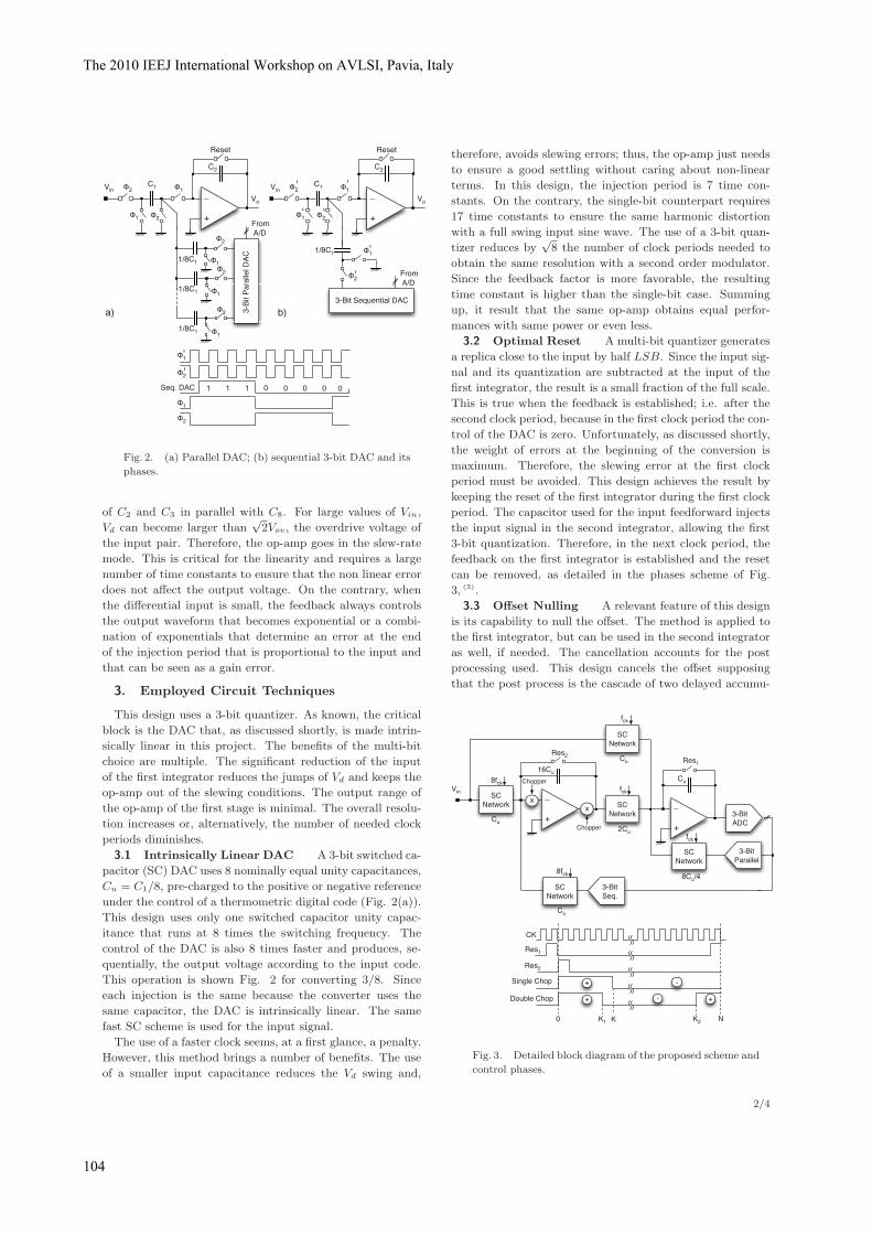
Fig. 2. (a) Parallel DAC; (b) sequential 3-bit DAC and its
phases.
of C2 and C3 in parallel with C8. For large values of Vin,
Vd can become larger than√2Vov, the overdrive voltage of
the input pair. Therefore, the op-amp goes in the slew-rate
mode. This is critical for the linearity and requires a large
number of time constants to ensure that the non linear error
does not affect the output voltage. On the contrary, when
the differential input is small, the feedback always controls
the output waveform that becomes exponential or a combi-
nation of exponentials that determine an error at the end
of the injection period that is proportional to the input and
that can be seen as a gain error.
3. Employed Circuit Techniques
This design uses a 3-bit quantizer. As known, the critical
block is the DAC that, as discussed shortly, is made intrin-
sically linear in this project. The benefits of the multi-bit
choice are multiple. The significant reduction of the input
of the first integrator reduces the jumps of Vd and keeps the
op-amp out of the slewing conditions. The output range of
the op-amp of the first stage is minimal. The overall resolu-
tion increases or, alternatively, the number of needed clock
periods diminishes.
3.1 Intrinsically Linear DAC A 3-bit switched ca-
pacitor (SC) DAC uses 8 nominally equal unity capacitances,
Cu = C1/8, pre-charged to the positive or negative reference
under the control of a thermometric digital code (Fig. 2(a)).
This design uses only one switched capacitor unity capac-
itance that runs at 8 times the switching frequency. The
control of the DAC is also 8 times faster and produces, se-
quentially, the output voltage according to the input code.
This operation is shown Fig. 2 for converting 3/8. Since
each injection is the same because the converter uses the
same capacitor, the DAC is intrinsically linear. The same
fast SC scheme is used for the input signal.
The use of a faster clock seems, at a first glance, a penalty.
However, this method brings a number of benefits. The use
of a smaller input capacitance reduces the Vd swing and,
therefore, avoids slewing errors; thus, the op-amp just needs
to ensure a good settling without caring about non-linear
terms. In this design, the injection period is 7 time con-
stants. On the contrary, the single-bit counterpart requires
17 time constants to ensure the same harmonic distortion
with a full swing input sine wave. The use of a 3-bit quan-
tizer reduces by√8 the number of clock periods needed to
obtain the same resolution with a second order modulator.
Since the feedback factor is more favorable, the resulting
time constant is higher than the single-bit case. Summing
up, it result that the same op-amp obtains equal perfor-
mances with same power or even less.
3.2 Optimal Reset A multi-bit quantizer generates
a replica close to the input by half LSB. Since the input sig-
nal and its quantization are subtracted at the input of the
first integrator, the result is a small fraction of the full scale.
This is true when the feedback is established; i.e. after the
second clock period, because in the first clock period the con-
trol of the DAC is zero. Unfortunately, as discussed shortly,
the weight of errors at the beginning of the conversion is
maximum. Therefore, the slewing error at the first clock
period must be avoided. This design achieves the result by
keeping the reset of the first integrator during the first clock
period. The capacitor used for the input feedforward injects
the input signal in the second integrator, allowing the first
3-bit quantization. Therefore, in the next clock period, the
feedback on the first integrator is established and the reset
can be removed, as detailed in the phases scheme of Fig.
3, (3).
3.3 Offset Nulling A relevant feature of this design
is its capability to null the offset. The method is applied to
the first integrator, but can be used in the second integrator
as well, if needed. The cancellation accounts for the post
processing used. This design cancels the offset supposing
that the post process is the cascade of two delayed accumu-
Fig. 3. Detailed block diagram of the proposed scheme and
control phases.
2/4
The 2010 IEEJ International Workshop on AVLSI, Pavia, Italy
104
lator. However, the extension of the technique to a cascade
of three integrators is straightforward.
A possible offset nulling technique uses a chopper (4) on
the first op-amp controlled by a fractal sequence, described
in (5). That method obtains the result under some constrains
on the number of clock periods. Here, the offset cancellation
is achieved with a single step chopping or, to obtain a better
accuracy, with two chopping steps.
Offset, Vos, is equivalent to a DC input signal. Its ef-
fect at the output of the two post processing accumulators
is VosN(N−1)/2 that, divided by the full scale amplitude
N(N−1)/2, obtains the input offset. A single chopping after
K clock cycles, as shown in Fig. 3, reverses the offset for the
remaining R = (N−K) clock periods. Therefore, the out-
put contributions of the offset before chopping and its one
reverse after chopping sum into
Vos
2[K(K − 1) + 2K(R− 1)− (R− 1)(R− 2)]; · · (1)
therefore, suitable values of N and K obtain a minimum of
the multiplying coefficient in (1).
It may happens that, for a given number of clock periods,
N , the corresponding K can obtain a not satisfactory resid-
ual offset. A better figure is obtained by a second chopping
(see Fig. 3) that generates a further positive term in (1)
suitable to trim the zeroing operation.
In real circuits, in addition to the input referred offset that
is reversed by chopping, there are small terms that give rise
to an offset in front of the chopper. They can be cancelled
out by a foreground calibration that sets the value of K (or
K1, K2).
4. Circuit Design
The fully differential version of the scheme of Fig. 3 has
been designed using a mixed 0.18-0.6 μm double-poly 6 metal
layers CMOS technology. The input signal is injected by a
SC structure running at 8fCK (fCK=1 MHz) synchronously
with the high speed sequential DAC (Fig. 2(b)). The DAC of
the second stage is a normal parallel architecture with ther-
mometric control (Fig. 2(a)). Since the mismatch between
unity elements of the second DAC is referred to the input
divided by (N−1), its effect is negligible. All the structures
of the second integrator use the slow clock.
The 3-bit flash uses 8 simple latched comparators. The
operational amplifiers are conventional telescopic cascode ca-
pable to reach a 120-dB gain and 18-MHz GBW. The 1/f
op-amp noise, assumed to fade below the sampling frequency,
is cancelled together with the offset.
The chosen value of the sampling capacitances is
Cu=Cin=CDAC=1.6 pF. In each fast clock period, the in-
jected square noise charge is 4kTCin. After a complete slow
clock period, the noise charge, injected 8 times on the 16Cu
of the first integrator, gives rise to an input referred noise
voltage v2n,in = kT/(2Cu), sharing a benefit of the average
over 8 fast clock periods. If the noise enters at clock pe-
riod K, its square contribution is amplified at the output by
(N −K − 1)2. Therefore, the quadratic superposition of all
the noise injections becomes V 2n,out = MkT/(2Cu), where
M =
N−1∑
i=1
i2 =(N − 1)3
3+
(N − 1)2
2+
(N − 1)
6· (2)
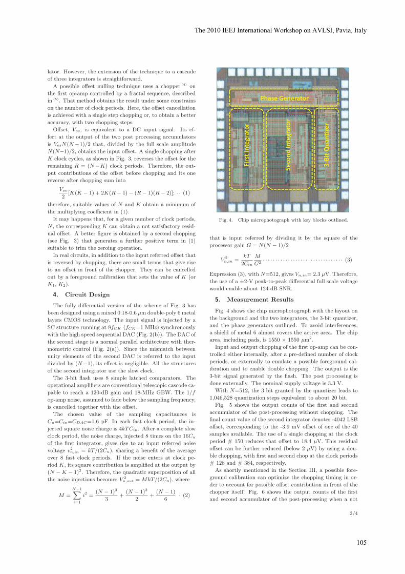
Fig. 4. Chip microphotograph with key blocks outlined.
that is input referred by dividing it by the square of the
processor gain G = N(N − 1)/2
V 2n,in =
kT
2Cin
M
G2· · · · · · · · · · · · · · · · · · · · · · · · · · · · · · · · (3)
Expression (3), with N=512, gives Vn,in= 2.3 μV. Therefore,
the use of a ±2-V peak-to-peak differential full scale voltage
would enable about 124-dB SNR.
5. Measurement Results
Fig. 4 shows the chip microphotograph with the layout on
the background and the two integrators, the 3-bit quantizer,
and the phase generators outlined. To avoid interferences,
a shield of metal 6 almost covers the active area. The chip
area, including pads, is 1550 × 1550 μm2.
Input and output chopping of the first op-amp can be con-
trolled either internally, after a pre-defined number of clock
periods, or externally to emulate a possible foreground cal-
ibration and to enable double chopping. The output is the
3-bit signal generated by the flash. The post processing is
done externally. The nominal supply voltage is 3.3 V.
With N=512, the 3 bit granted by the quantizer leads to
1,046,528 quantization steps equivalent to about 20 bit.
Fig. 5 shows the output counts of the first and second
accumulator of the post-processing without chopping. The
final count value of the second integrator denotes -4042 LSB
offset, corresponding to the -3.9 mV offset of one of the 40
samples available. The use of a single chopping at the clock
period # 150 reduces that offset to 18.4 μV. This residual
offset can be further reduced (below 2 μV) by using a dou-
ble chopping, with first and second chop at the clock periods
# 128 and # 384, respectively.
As shortly mentioned in the Section III, a possible fore-
ground calibration can optimize the chopping timing in or-
der to account for possible offset contribution in front of the
chopper itself. Fig. 6 shows the output counts of the first
and second accumulator of the post-processing when a not
3/4
The 2010 IEEJ International Workshop on AVLSI, Pavia, Italy
105
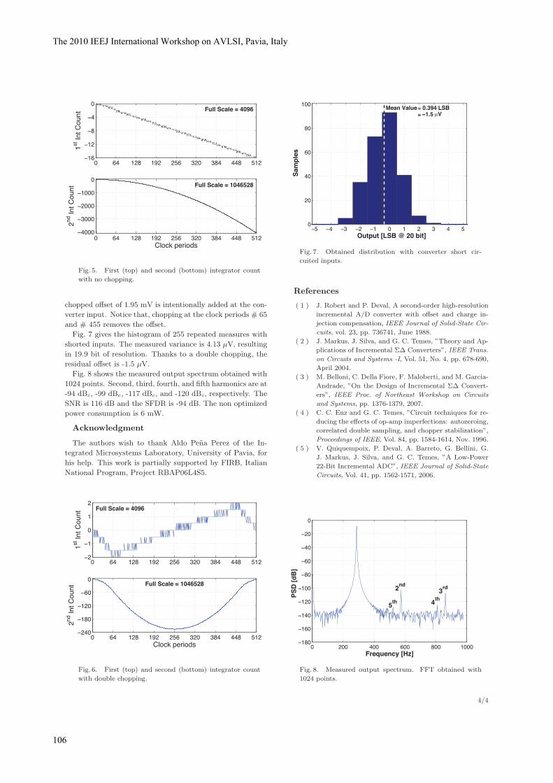
Fig. 5. First (top) and second (bottom) integrator count
with no chopping.
chopped offset of 1.95 mV is intentionally added at the con-
verter input. Notice that, chopping at the clock periods # 65
and # 455 removes the offset.
Fig. 7 gives the histogram of 255 repeated measures with
shorted inputs. The measured variance is 4.13 μV, resulting
in 19.9 bit of resolution. Thanks to a double chopping, the
residual offset is -1.5 μV.
Fig. 8 shows the measured output spectrum obtained with
1024 points. Second, third, fourth, and fifth harmonics are at
-94 dBc, -99 dBc, -117 dBc, and -120 dBc, respectively. The
SNR is 116 dB and the SFDR is -94 dB. The non optimized
power consumption is 6 mW.
Acknowledgment
The authors wish to thank Aldo Pena Perez of the In-
tegrated Microsystems Laboratory, University of Pavia, for
his help. This work is partially supported by FIRB, Italian
National Program, Project RBAP06L4S5.
Fig. 6. First (top) and second (bottom) integrator count
with double chopping.
−5 −4 −3 −2 −1 0 1 2 3 4 50
20
40
60
80
100Mean Value ≅ 0.394⋅LSB
≅ −1.5 μV
Output [LSB @ 20 bit]
Sam
ple
s
Fig. 7. Obtained distribution with converter short cir-
cuited inputs.
References
( 1 ) J. Robert and P. Deval, A second-order high-resolution
incremental A/D converter with offset and charge in-
jection compensation, IEEE Journal of Solid-State Cir-
cuits, vol. 23, pp. 736741, June 1988.
( 2 ) J. Markus, J. Silva, and G. C. Temes, ”Theory and Ap-
plications of Incremental ΣΔ Converters”, IEEE Trans.
on Circuits and Systems -I, Vol. 51, No. 4, pp. 678-690,
April 2004.
( 3 ) M. Belloni, C. Della Fiore, F. Maloberti, and M. Garcia-
Andrade, ”On the Design of Incremental ΣΔ Convert-
ers”, IEEE Proc. of Northeast Workshop on Circuits
and Systems, pp. 1376-1379, 2007.
( 4 ) C. C. Enz and G. C. Temes, ”Circuit techniques for re-
ducing the effects of op-amp imperfections: autozeroing,
correlated double sampling, and chopper stabilization”,
Proceedings of IEEE, Vol. 84, pp. 1584-1614, Nov. 1996.
( 5 ) V. Quiquempoix, P. Deval, A. Barreto, G. Bellini, G.
J. Markus, J. Silva, and G. C. Temes, ”A Low-Power
22-Bit Incremental ADC”, IEEE Journal of Solid-State
Circuits, Vol. 41, pp. 1562-1571, 2006.
0 200 400 600 800 1000−180
−160
−140
−120
−100
−80
−60
−40
−20
0
Frequency [Hz]
PS
D [
dB
]
2nd
3rd
4th
5th
Fig. 8. Measured output spectrum. FFT obtained with
1024 points.
4/4
The 2010 IEEJ International Workshop on AVLSI, Pavia, Italy
106