High Performance ${ eta}$ -Ga 2 O 3 Nano-Membrane Field ... › ~yep › Papers › IEEE... · a...
5
Received 12 April 2019; revised 20 June 2019 and 26 July 2019; accepted 28 July 2019. Date of publication 6 August 2019; date of current version 30 August 2019. The review of this article was arranged by Editor C.-M. Zetterling. Digital Object Identifier 10.1109/JEDS.2019.2933369 High Performance β -Ga 2 O 3 Nano-Membrane Field Effect Transistors on a High Thermal Conductivity Diamond Substrate JINHYUN NOH 1,2 , SAMI ALAJLOUNI 1,2 , MARKO J. TADJER 3 (Senior Member, IEEE), JAMES C. CULBERTSON 3 , HAGYOUL BAE 1,2 (Member, IEEE), MENGWEI SI 1,2 , HONG ZHOU 1,2 , PETER A. BERMEL 1,2 , ALI SHAKOURI 1,2 , AND PEIDE D. YE 1,2 (Fellow, IEEE) 1 School of Electrical and Computer Engineering, Purdue University, West Lafayette, IN 47907, USA 2 Birck Nanotechnology Center, Purdue University, West Lafayette, IN47907, USA 3 Electronics Science and Technology Division, United States Naval Research Laboratory, Washington, DC 20375, USA CORRESPONDING AUTHOR: P. YE (e-mail: [email protected]) This work was supported in part by ASCENT, one of six centers in JUMP, a Semiconductor Research Corporation Program sponsored by DARPA, in part by the Office of Naval Research’s Naval Enterprise Partnership Teaming with Universities for National Excellence under Grant N00014-15-1-2833, and in part by the Defense Threat Reduction Agency under Grant HDTRA1-12-1-0025. ABSTRACT To suppress severe self-heating under high power density, we herein demonstrate top-gate nano-membrane β -gallium oxide (β -Ga 2 O 3 ) field effect transistors on a high thermal conductivity diamond substrate. The devices exhibit enhanced performance, with a record high maximum drain current of 980 mA/mm for top-gate β -Ga 2 O 3 field effect transistors and 60% less temperature increase from reduced self-heating, compared to the device on a sapphire substrate operating under identical power density. With improved heat dissipation, β -Ga 2 O 3 field effect transistors on a diamond substrate are validated using an ultrafast high-resolution thermoreflectance imaging technique, Raman thermography, and thermal simulations. INDEX TERMS β -Ga 2 O 3 FET, diamond, nano-membrane, thermal conductivity, self-heating effect. I. INTRODUCTION β -Ga 2 O 3 is an emerging wide bandgap semiconductor for the next generation power devices to replace GaN and SiC. It has an ultra-wide bandgap of 4.8 eV and a corresponding high breakdown field (E br ) of 8 MV/cm [1]–[5]. And low-cost large-size β -Ga 2 O 3 native bulk substrates can be poten- tially realized by melt-grown methods [6]–[7]. However, the β -Ga 2 O 3 bulk substrate has a low thermal conduc- tivity (κ ) of 10-25 W/m·K and thus severe self-heating effects (SHE) can be observed [8]. In high-power electronic devices, the output power density (P) and maximum drain current (I D ) can be significantly limited by elevated chan- nel temperature caused by SHE [9], [10] and it has become a key challenges in β -Ga 2 O 3 research because elevated temperature degrades electron mobility in β -Ga 2 O 3 [8], [11]–[13]. In addition, high channel temperature can also severely degrade the gate dielectric, device variability, and long-term reliability [8], [14]. Recently, various stud- ies regarding the thermal management of β -Ga 2 O 3 devices have been reported [15]–[17]. In particular, it is important to mitigate SHE to sustain original device performance of β -Ga 2 O 3 devices in practical applications. One solution is an integration of a low κβ -Ga 2 O 3 channel on a high κ sub- strate, rather than taking advantages of the β -Ga 2 O 3 native substrate. In our previous works, we have demonstrated β -Ga 2 O 3 field effect transistors (FETs) on a sapphire substrate (κ = 40 W/m·K) to replace a SiO 2 /Si substrate (κ = 1.5 W/m·K for 270 nm SiO 2 ) [18]–[20]. The resulting device has shown a 70% higher maximum I D , half the device surface temper- ature increase (T), and half the thermal resistance (R T ), significantly reducing SHE in comparison to a SiO 2 /Si sub- strate. Diamond has a much higher thermal conductivity (κ = 1, 000-2, 200 W/m·K) than sapphire; thus, it is of 2168-6734 c 2019 IEEE. Translations and content mining are permitted for academic research only. Personal use is also permitted, but republication/redistribution requires IEEE permission. 914 See http://www.ieee.org/publications_standards/publications/rights/index.html for more information. VOLUME 7, 2019
Transcript of High Performance ${ eta}$ -Ga 2 O 3 Nano-Membrane Field ... › ~yep › Papers › IEEE... · a...
Received 12 April 2019; revised 20 June 2019 and 26 July 2019; accepted 28 July 2019. Date of publication 6 August 2019; date of current version30 August 2019. The review of this article was arranged by Editor C.-M. Zetterling.
Digital Object Identifier 10.1109/JEDS.2019.2933369
High Performance β-Ga2O3 Nano-MembraneField Effect Transistors on a High Thermal
Conductivity Diamond SubstrateJINHYUN NOH 1,2, SAMI ALAJLOUNI 1,2, MARKO J. TADJER 3 (Senior Member, IEEE),
JAMES C. CULBERTSON3, HAGYOUL BAE 1,2 (Member, IEEE), MENGWEI SI 1,2, HONG ZHOU 1,2,PETER A. BERMEL1,2, ALI SHAKOURI1,2, AND PEIDE D. YE 1,2 (Fellow, IEEE)
1 School of Electrical and Computer Engineering, Purdue University, West Lafayette, IN 47907, USA2 Birck Nanotechnology Center, Purdue University, West Lafayette, IN 47907, USA
3 Electronics Science and Technology Division, United States Naval Research Laboratory, Washington, DC 20375, USA
CORRESPONDING AUTHOR: P. YE (e-mail: [email protected])
This work was supported in part by ASCENT, one of six centers in JUMP, a Semiconductor Research Corporation Program sponsored by DARPA, in part by the
Office of Naval Research’s Naval Enterprise Partnership Teaming with Universities for National Excellence under Grant N00014-15-1-2833,
and in part by the Defense Threat Reduction Agency under Grant HDTRA1-12-1-0025.
ABSTRACT To suppress severe self-heating under high power density, we herein demonstrate top-gatenano-membrane β-gallium oxide (β-Ga2O3) field effect transistors on a high thermal conductivity diamondsubstrate. The devices exhibit enhanced performance, with a record high maximum drain current of980 mA/mm for top-gate β-Ga2O3 field effect transistors and 60% less temperature increase from reducedself-heating, compared to the device on a sapphire substrate operating under identical power density.With improved heat dissipation, β-Ga2O3 field effect transistors on a diamond substrate are validatedusing an ultrafast high-resolution thermoreflectance imaging technique, Raman thermography, and thermalsimulations.
INDEX TERMS β-Ga2O3FET, diamond, nano-membrane, thermal conductivity, self-heating effect.
I. INTRODUCTIONβ-Ga2O3 is an emerging wide bandgap semiconductor for thenext generation power devices to replace GaN and SiC. It hasan ultra-wide bandgap of 4.8 eV and a corresponding highbreakdown field (Ebr) of 8 MV/cm [1]–[5]. And low-costlarge-size β-Ga2O3 native bulk substrates can be poten-tially realized by melt-grown methods [6]–[7]. However,the β-Ga2O3 bulk substrate has a low thermal conduc-tivity (κ) of 10-25 W/m·K and thus severe self-heatingeffects (SHE) can be observed [8]. In high-power electronicdevices, the output power density (P) and maximum draincurrent (ID) can be significantly limited by elevated chan-nel temperature caused by SHE [9], [10] and it has becomea key challenges in β-Ga2O3 research because elevatedtemperature degrades electron mobility in β-Ga2O3 [8],[11]–[13]. In addition, high channel temperature can alsoseverely degrade the gate dielectric, device variability,
and long-term reliability [8], [14]. Recently, various stud-ies regarding the thermal management of β-Ga2O3 deviceshave been reported [15]–[17]. In particular, it is importantto mitigate SHE to sustain original device performance ofβ-Ga2O3 devices in practical applications. One solution isan integration of a low κ β-Ga2O3 channel on a high κ sub-strate, rather than taking advantages of the β-Ga2O3 nativesubstrate.In our previous works, we have demonstrated β-Ga2O3
field effect transistors (FETs) on a sapphire substrate (κ =40 W/m·K) to replace a SiO2/Si substrate (κ = 1.5 W/m·Kfor 270 nm SiO2) [18]–[20]. The resulting device has showna 70% higher maximum ID, half the device surface temper-ature increase (�T), and half the thermal resistance (RT),significantly reducing SHE in comparison to a SiO2/Si sub-strate. Diamond has a much higher thermal conductivity(κ = 1, 000-2, 200 W/m·K) than sapphire; thus, it is of
2168-6734 c© 2019 IEEE. Translations and content mining are permitted for academic research only.Personal use is also permitted, but republication/redistribution requires IEEE permission.
914 See http://www.ieee.org/publications_standards/publications/rights/index.html for more information. VOLUME 7, 2019
NOH et al.: HIGH PERFORMANCE β-Ga2O3 NANO-MEMBRANE FETs
great interest to investigate the heat dissipation effect of β-Ga2O3 devices on a diamond substrate. Diamond is alsoa current blocking substrate for transferred β-Ga2O3 nano-membranes due to its wide bandgap of 5.47eV [21]. In thiswork, we not only demonstrate the record performance oftop-gate β-Ga2O3 FETs on a diamond substrate [22], [23],but also fully study the thermal properties of β-Ga2O3on a diamond substrate using high-resolution thermore-flectance (TR) imaging [24], [25], Raman thermography,and thermal simulations.
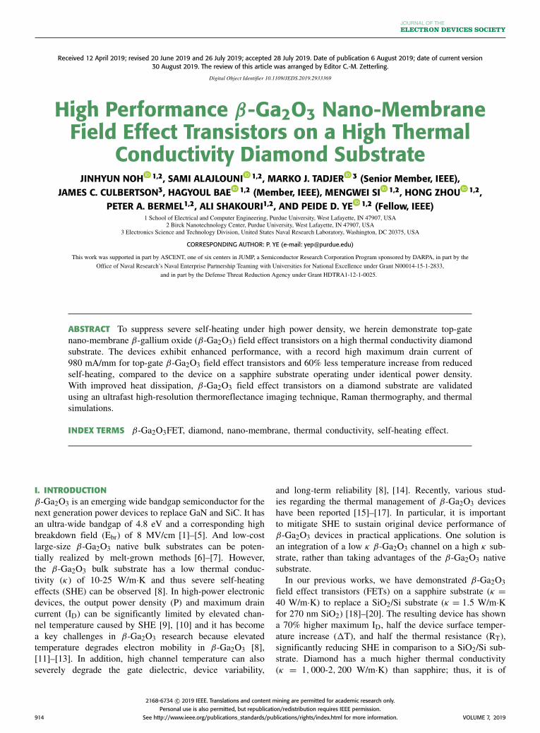
FIGURE 1. (a) Schematic view of a top-gate β-Ga2O3 FET on a diamondsubstrate. (b) SEM top view of a β-Ga2O3 FET with LG = 1 µm. (c) Thermalequilibrium energy band diagram of a β-Ga2O3 FET from the gate to thediamond substrate.
II. DEVICE FABRICATION AND I–V CHARACTERISTICSFig. 1(a) and (b) are the schematic view and the top-viewscanning electron microscopy (SEM) image of a top-gateβ-Ga2O3 transistor on a diamond substrate. β-Ga2O3 nano-membranes with thicknesses from 50-150 nm (100), Sn-doped at 2.7 × 1018 cm−3 were transferred to a 500 µm-thick polished (100) diamond bulk single crystal substrate.A Ti/Al/Au (15/60/50 nm) metal stack was deposited andlifted-off in source and drain regions for the source anddrain contact formation. The top-gate stack consists of 15 nmamorphous aluminum oxide (Al2O3) gate dielectric depositedby atomic layer deposition (ALD) at 175 ◦C and Ni/Au(50/50 nm) as the gate electrode. All the source, drain, andgate regions were patterned by electron-beam lithography.Fig. 1(c) shows the energy band line-up from the gate allthe way to the diamond substrate of a fabricated top-gateβ-Ga2O3 transistor on a diamond substrate.The output and transfer characteristics of a representative
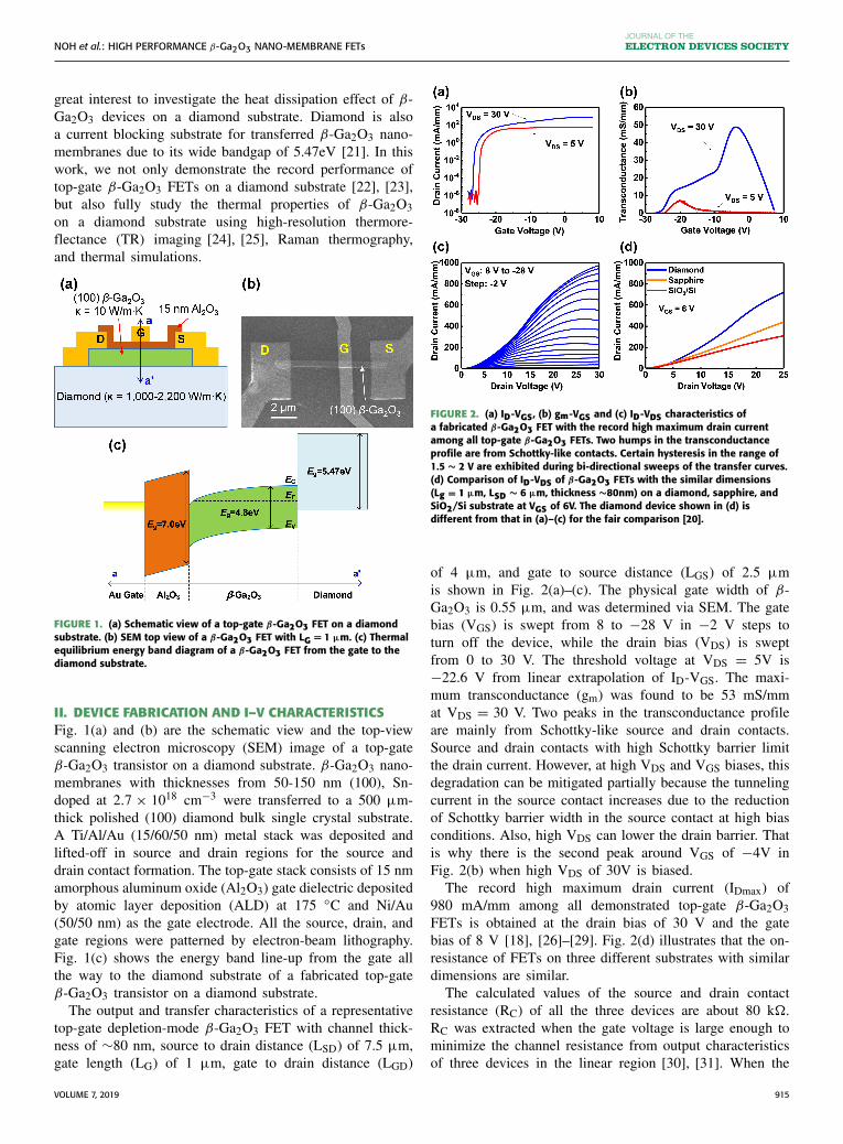
top-gate depletion-mode β-Ga2O3 FET with channel thick-ness of ∼80 nm, source to drain distance (LSD) of 7.5 µm,gate length (LG) of 1 µm, gate to drain distance (LGD)
FIGURE 2. (a) ID-VGS, (b) gm-VGS and (c) ID-VDS characteristics ofa fabricated β-Ga2O3 FET with the record high maximum drain currentamong all top-gate β-Ga2O3 FETs. Two humps in the transconductanceprofile are from Schottky-like contacts. Certain hysteresis in the range of1.5 ∼ 2 V are exhibited during bi-directional sweeps of the transfer curves.(d) Comparison of ID-VDS of β-Ga2O3 FETs with the similar dimensions(Lg = 1 µm, LSD ∼ 6 µm, thickness ∼80nm) on a diamond, sapphire, andSiO2/Si substrate at VGS of 6V. The diamond device shown in (d) isdifferent from that in (a)–(c) for the fair comparison [20].
of 4 µm, and gate to source distance (LGS) of 2.5 µmis shown in Fig. 2(a)–(c). The physical gate width of β-Ga2O3 is 0.55 µm, and was determined via SEM. The gatebias (VGS) is swept from 8 to −28 V in −2 V steps toturn off the device, while the drain bias (VDS) is sweptfrom 0 to 30 V. The threshold voltage at VDS = 5V is−22.6 V from linear extrapolation of ID-VGS. The maxi-mum transconductance (gm) was found to be 53 mS/mmat VDS = 30 V. Two peaks in the transconductance profileare mainly from Schottky-like source and drain contacts.Source and drain contacts with high Schottky barrier limitthe drain current. However, at high VDS and VGS biases, thisdegradation can be mitigated partially because the tunnelingcurrent in the source contact increases due to the reductionof Schottky barrier width in the source contact at high biasconditions. Also, high VDS can lower the drain barrier. Thatis why there is the second peak around VGS of −4V inFig. 2(b) when high VDS of 30V is biased.The record high maximum drain current (IDmax) of
980 mA/mm among all demonstrated top-gate β-Ga2O3FETs is obtained at the drain bias of 30 V and the gatebias of 8 V [18], [26]–[29]. Fig. 2(d) illustrates that the on-resistance of FETs on three different substrates with similardimensions are similar.The calculated values of the source and drain contact
resistance (RC) of all the three devices are about 80 k�.RC was extracted when the gate voltage is large enough tominimize the channel resistance from output characteristicsof three devices in the linear region [30], [31]. When the
VOLUME 7, 2019 915
NOH et al.: HIGH PERFORMANCE β-Ga2O3 NANO-MEMBRANE FETs
power density is increased by increased drain voltage, thedrain current level becomes significantly different dependingon substrates.The obtained high drain current can be ascribed mainly to
the improved transport properties at lower channel temper-atures from significantly reduced SHE. The heat generatedin the channel under high bias dissipates much faster ona diamond substrate, compared to SiO2/Si and sapphire sub-strates. The electron mobility of β-Ga2O3 decreases whenthe temperature increases above room temperature so thatthis improved transport properties by less self-heating effecton a diamond substrate could be the main reason for theincrease of the maximum drain current [12].
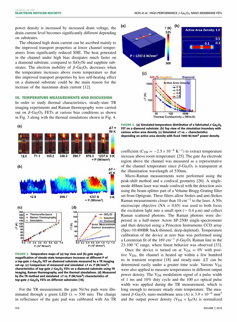
III. TEMPERATURE MEASUREMENTS AND DISCUSSIONIn order to study thermal characteristics, steady-state TRimaging experiments and Raman thermography were carriedout on β-Ga2O3 FETs at various bias conditions as shownin Fig. 3 along with the thermal simulations shown in Fig. 4.
FIGURE 3. Temperature maps of (a) top view and (b) gate regionmagnification of steady-state temperature increases at different P ofa top-gate β-Ga2O3 FET on diamond substrate measured by a TR imagingset-up. (c) Comparison of measured and simulated �T vs. P (W/mm2)characteristics of top-gate β-Ga2O3 FETs on a diamond substrate using TRimaging, Raman thermography, and the thermal simulations. (d) Measuredby the TR method and simulated �T vs. P (W/mm2) characteristics oftop-gate β-Ga2O3 FETs on different substrates [18].
For the TR measurement, the gate Ni/Au pads were illu-minated through a green LED (λ = 530 nm). The changein reflectance of the gate pad was calibrated with Au TR
FIGURE 4. (a) Simulated temperature distribution of a fabricated β-Ga2O3FET on a diamond substrate. (b) Top view of the simulation boundary withvarious active area density. (c) Simulated �T vs. κ characteristicsdepending on active area density with fixed 1000 W/mm2 power density.
coefficient (CTH = −2.5×10⁻⁴ K−1) to extract temperatureincrease above room temperature [25]. The gate Au electroderegion above the channel was measured as a representativeof the channel temperature since β-Ga2O3 is transparent atthe illumination wavelength of 530nm.Micro-Raman measurements were performed using the
peak-shift method and a confocal geometry [26]. A single-mode 488nm laser was made confocal with the detection axisusing the beam-splitter part of a Volume-Bragg-Grating filterset from Optigrate. These filters allow Stokes and anti-StokesRaman measurements closer than 10 cm−1 to the laser. A 50xmicroscope objective (NA = 0.65) was used to both focusthe excitation light into a small spot (∼ 0.4 µm) and collectRaman scattered photons. The Raman photons were dis-persed in a half-meter Acton SP-2500 single-spectrometerand then detected using a Princeton Instruments CCD array(Spec-10:400BR back-thinned, deep-depleted). Temperaturecalibration of the device at zero bias was performed usinga Lorentzian fit of the 169 cm−1 β-Ga2O3 Raman line in the23-100 ◦C range, where linear behavior was observed [33].Once the device is turned on at VGS = 0V with posi-
tive VDS, the channel is heated up within a few hundredns in transient response [18] and steady-state �T can bedetermined easily under a greater time scale. Various VDSwere also applied to measure temperatures in different outputpower density. The VDS modulation signal of a pulse widthof 1 ms and 10% duty cycle and the 100 µs optical pulsewidth was applied during the TR measurement, which islong enough to measure steady state temperature. The mea-sured β-Ga2O3 nano-membrane area (A) is 3.9×10⁻⁶ mm2
and the output power density (VDS × ID/A) is normalized
916 VOLUME 7, 2019
NOH et al.: HIGH PERFORMANCE β-Ga2O3 NANO-MEMBRANE FETs
by area (W × LSD) to avoid different heat dissipation areasfrom different sizes of β-Ga2O3 nano-membranes for accu-rate comparison. The bias conditions of each temperaturemeasurement point in Fig. 3(a) are summarized in Table 1.
TABLE 1. Bias conditions of each temperature measurement point in
Fig. 3(a).
Fig. 3(c) shows the measured and simulated �T vs.P (W/mm2) for the β-Ga2O3 FETs on a diamond sub-strate, performed both by TR imaging and Raman ther-mography. The thermal simulations were carried out usingthe COMSOL commercial finite-element analysis softwarepackage [34]. Agreement among these three methods wasobserved, with the highest temperature measured by Ramanthermography to be 164 ◦C (�T = 141 K) at DC outputpower of 6,565 W/mm2 (64.7 W/mm or VDS = 35 V forthis particular exfoliated FET geometry). Fig. 3(d) showsagreement of the TR measured and the simulated �T vs.P (W/mm2) on different substrates. Except substrates, allprocess and materials including the doping concentration ofβ-Ga2O3 are exactly the same. The devices with similardimensions (Lg = 1 µm, LSD ∼ 6 µm, thickness ∼ 80 nm)for each substrate are selected for thermal measurement. Theoutput power density of devices on three different substratesare normalized by the area of the device to make a faircomparison.Thermal simulations were carried out using COMSOL
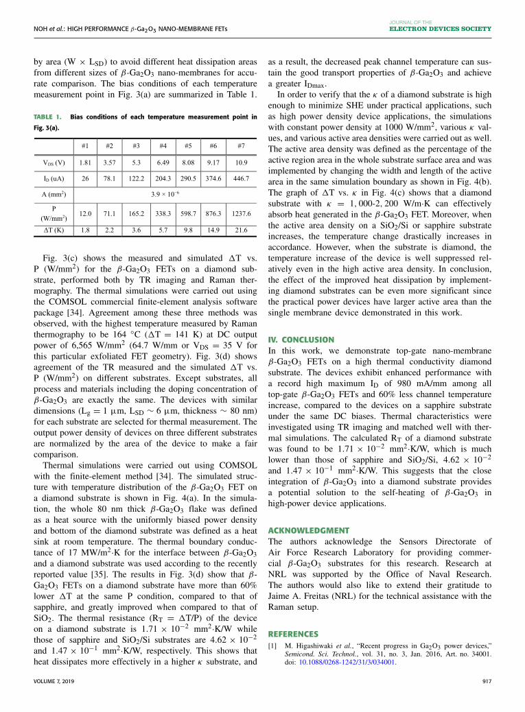
with the finite-element method [34]. The simulated struc-ture with temperature distribution of the β-Ga2O3 FET ona diamond substrate is shown in Fig. 4(a). In the simula-tion, the whole 80 nm thick β-Ga2O3 flake was definedas a heat source with the uniformly biased power densityand bottom of the diamond substrate was defined as a heatsink at room temperature. The thermal boundary conduc-tance of 17 MW/m2·K for the interface between β-Ga2O3and a diamond substrate was used according to the recentlyreported value [35]. The results in Fig. 3(d) show that β-Ga2O3 FETs on a diamond substrate have more than 60%lower �T at the same P condition, compared to that ofsapphire, and greatly improved when compared to that ofSiO2. The thermal resistance (RT = �T/P) of the deviceon a diamond substrate is 1.71 × 10⁻² mm2·K/W whilethose of sapphire and SiO2/Si substrates are 4.62 × 10⁻²
and 1.47 × 10⁻¹ mm2·K/W, respectively. This shows thatheat dissipates more effectively in a higher κ substrate, and
as a result, the decreased peak channel temperature can sus-tain the good transport properties of β-Ga2O3 and achievea greater IDmax.In order to verify that the κ of a diamond substrate is high
enough to minimize SHE under practical applications, suchas high power density device applications, the simulationswith constant power density at 1000 W/mm2, various κ val-ues, and various active area densities were carried out as well.The active area density was defined as the percentage of theactive region area in the whole substrate surface area and wasimplemented by changing the width and length of the activearea in the same simulation boundary as shown in Fig. 4(b).The graph of �T vs. κ in Fig. 4(c) shows that a diamondsubstrate with κ = 1, 000-2, 200 W/m·K can effectivelyabsorb heat generated in the β-Ga2O3 FET. Moreover, whenthe active area density on a SiO2/Si or sapphire substrateincreases, the temperature change drastically increases inaccordance. However, when the substrate is diamond, thetemperature increase of the device is well suppressed rel-atively even in the high active area density. In conclusion,the effect of the improved heat dissipation by implement-ing diamond substrates can be even more significant sincethe practical power devices have larger active area than thesingle membrane device demonstrated in this work.
IV. CONCLUSIONIn this work, we demonstrate top-gate nano-membraneβ-Ga2O3 FETs on a high thermal conductivity diamondsubstrate. The devices exhibit enhanced performance witha record high maximum ID of 980 mA/mm among alltop-gate β-Ga2O3 FETs and 60% less channel temperatureincrease, compared to the devices on a sapphire substrateunder the same DC biases. Thermal characteristics wereinvestigated using TR imaging and matched well with ther-mal simulations. The calculated RT of a diamond substratewas found to be 1.71 × 10⁻² mm2·K/W, which is muchlower than those of sapphire and SiO2/Si, 4.62 × 10⁻²
and 1.47 × 10⁻¹ mm2·K/W. This suggests that the closeintegration of β-Ga2O3 into a diamond substrate providesa potential solution to the self-heating of β-Ga2O3 inhigh-power device applications.
ACKNOWLEDGMENTThe authors acknowledge the Sensors Directorate ofAir Force Research Laboratory for providing commer-cial β-Ga2O3 substrates for this research. Research atNRL was supported by the Office of Naval Research.The authors would also like to extend their gratitude toJaime A. Freitas (NRL) for the technical assistance with theRaman setup.
REFERENCES[1] M. Higashiwaki et al., “Recent progress in Ga2O3 power devices,”
Semicond. Sci. Technol., vol. 31, no. 3, Jan. 2016, Art. no. 34001.doi: 10.1088/0268-1242/31/3/034001.
VOLUME 7, 2019 917
NOH et al.: HIGH PERFORMANCE β-Ga2O3 NANO-MEMBRANE FETs
[2] S. I. Stepanov, V. I. Nikolaev, V. E. Bougrov, and A. E. Romanov,“Gallium oxide: Properties and applications—A review,” Rev.Adv. Mater. Sci., vol. 44, no. 63, pp. 63–86, Apr. 2016.[Online]. Available: http://www.ipme.ru/e-journals/RAMS/no_14416/06_14416_stepanov.pdf
[3] M. Kim, J.-H. Seo, U. Singisetti, and Z. Ma, “Recent advancesin free-standing single crystalline wide band-gap semiconductorsand their applications: GaN, SiC, ZnO, β-Ga2O3, and diamond,”J. Mater. Chem. C, vol. 5, no. 33, pp. 8338–8354, Jun. 2017.doi: 10.1039/C7TC02221B.
[4] S. J. Pearton et al., “A review of Ga2O3 materials, processing, anddevices,” Appl. Phys. Rev., vol. 5, no. 1, Jan. 2018, Art. no. 11301.doi: 10.1063/1.5006941.
[5] M. Higashiwaki and G. H. Jessen, “Guest editorial: The dawn ofgallium oxide microelectronics,” Appl. Phys. Lett., vol. 112, no. 6,Feb. 2018, Art. no. 060401. doi: 10.1063/1.5017845.
[6] H. Aida, K. Nishiguchi, H. Takeda, N. Aota, K. Sunakawa, andY. Yaguchi, “Growth of β-Ga2O3 single crystals by the edge-defined,film fed growth method,” Jpn. J. Appl. Phys., vol. 47, no. 11,pp. 8506–8509, Nov. 2008. doi: 10.1143/JJAP.47.8506.
[7] Z. Galazka et al., “On the bulk β-Ga2O3 single crystals grown bythe Czochralski method,” J. Cryst. Growth, vol. 404, pp. 184–191,Oct. 2014. doi: 10.1016/j.jcrysgro.2014.07.021.
[8] M. H. Wong, Y. Morikawa, K. Sasaki, A. Kuramata, S. Yamakoshi, andM. Higashiwaki, “Characterization of channel temperature in Ga2O3metal-oxide-semiconductor field-effect transistors by electrical mea-surements and thermal modeling,” Appl. Phys. Lett., vol. 109, no. 19,Nov. 2016, Art. no. 193503. doi: 10.1063/1.4966999.
[9] R. Gaska, A. Osinsky, J. W. Yang, and M. S. Shur, “Self-heating inhigh-power AlGaN-GaN HFETs,” IEEE Electron Device Lett., vol. 19,no. 3, pp. 89–91, Mar. 1998. doi: 10.1109/55.661174.
[10] Y. Zhou et al., “Thermal characterization of polycrystalline diamondthin film heat spreaders grown on GaN HEMTs,” Appl. Phys. Lett.,vol. 111, no. 4, Jul. 2017, Art. no 041901. doi: 10.1063/1.4995407.
[11] K. Irmscher, Z. Galazka, M. Pietsch, R. Uecker, and R. Fornari,“Electrical properties of β-Ga2O3 single crystals grown by theCzochralski method,” J. Appl. Phys., vol. 110, no. 6, Sep. 2011,Art. no. 063720. doi: 10.1063/1.3642962.
[12] T. Oishi, Y. Koga, K. Harada, and M. Kasu, “High-mobilityβ-Ga2O3(-201) single crystals grown by edge-defined film-fedgrowth method and their Schottky barrier diodes with Ni con-tact,” Appl. Phys. Exp., vol. 8, no. 3, Feb. 2015, Art. no. 031101.doi: 10.7567/APEX.8.031101.
[13] A. Parisini and R. Fornari, “Analysis of the scattering mech-anisms controlling electron mobility in β-Ga2O3,” Semicond.Sci. Technol., vol. 31, no. 3, Feb. 2016, Art. no. 035023.doi: 10.1088/0268-1242/31/3/035023.
[14] R. J. Trew, D. S. Green, and J. B. Shealy, “AlGaN/GaN HFET reli-ability,” IEEE Microw. Mag., vol. 10, no. 4, pp. 116–127, Jun. 2009.doi: 10.1109/MMM.2009.932286.
[15] B. Chatterjee, K. Zeng, C. D. Nordquist, U. Singisetti, and S. Choi,“Device-level thermal management of gallium oxide field-effecttransistors,” IEEE Trans. Compon. Packag. Manuf. Technol., to bepublished. doi: 10.1109/TCPMT.2019.2923356.
[16] J. W. Pomeroy et al., “Raman thermography of peak channel temper-ature in β-Ga2O3 MOSFETs,” IEEE Electron Device Lett., vol. 40,no. 2, pp. 189–192, Feb. 2019. doi: 10.1109/LED.2018.2887278.
[17] M. J. Tadjer, “Cheap ultra-wide bandgap power electronics? Galliumoxide May hold the answer,” Electrochem. Soc. Interface, vol. 27,no. 4, pp. 49–52, 2018. doi: 10.1149/2.F05184if.
[18] H. Zhou, K. Maize, J. Noh, A. Shakouri, and P. D. Ye,“Thermodynamic studies of β-Ga2O3 nanomembrane field-effecttransistors on a sapphire substrate,” ACS Omega, vol. 2, no. 11,pp. 7723–7729, Nov. 2017. doi: 10.1021/acsomega.7b01313.
[19] H. Zhou, M. Si, S. Alghamdi, G. Qiu, L. Yang, andP. D. Ye, “High-performance depletion/enhancement-modeβ-Ga2O3 on insulator (GOOI) field-effect transistors withrecord drain currents of 600/450 mA/mm,” IEEE ElectronDevice Lett., vol. 38, no. 1, pp. 103–106, Jan. 2017.doi: 10.1109/LED.2016.2635579.
[20] H. Zhou, K. Maize, G. Qiu, A. Shakouri, and P. D. Ye,“β-Ga2O3 on insulator field-effect transistors with drain cur-rents exceeding 1.5 A/mm and their self-heating effect,” Appl.Phys. Lett., vol. 111, no. 9, Aug. 2017, Art. no. 92102.doi: 10.1063/1.5000735.
[21] S. V. Kidalov and F. M. Shakhov, “Thermal conductivity of diamondcomposites,” Mater. (Basel), vol. 2, no. 4, pp. 2467–2495, Dec. 2009.doi: 10.3390/ma2042467.
[22] J. Noh et al., “β-Ga2O3 nano-membrane FETs on a diamond sub-strate,” in Proc. Compound Semicond. Week (CSW), May 2018,pp. 451–452.
[23] J. Noh, M. Si, H. Zhou, M. J. Tadjer, and P. D. Ye, “Theimpact of substrates on the performance of to-gate β-Ga2O3field-effect transistors: Record high drain current of 980 mA/mmon diamond,” in Proc. Device Res. Conf. (DRC), Jun. 2018.doi: 10.1109/DRC.2018.8442276.
[24] M. Farzaneh et al., “CCD-based thermoreflectance microscopy:Principles and applications,” J. Phys. D Appl. Phys., vol. 42, no. 14,Jun. 2009, Art. no. 143001. doi: 10.1088/0022-3727/42/14/143001.
[25] K. Maize, A. Ziabari, W. D. French, P. Lindorfer, B. Oconnell, andA. Shakouri, “Thermoreflectance CCD imaging of self-heating inpower MOSFET arrays,” IEEE Trans. Electron Devices, vol. 61, no. 9,pp. 3047–3053, Sep. 2014. doi: 10.1109/TED.2014.2332466.
[26] B. Chatterjee, A. Jayawardena, E. Heller, D. W. Snyder, S. Dhar,and S. Choi, “Thermal characterization of gallium oxide Schottkybarrier diodes,” Rev. Sci. Instrum., vol. 89, no. 11, Nov. 2018,Art. no. 114903. doi: 10.1063/1.5053621.
[27] A. J. Green et al., “3.8-MV/cm breakdown strength of MOVPE-grownSn-doped β-Ga2O3 MOSFETs,” IEEE Electron Device Lett., vol. 37,no. 7, pp. 902–905, Jul. 2016. doi: 10.1109/LED.2016.2568139.
[28] N. A. Moser et al., “High pulsed current density β-Ga2O3 MOSFETsverified by an analytical model corrected for interface charge,”Appl. Phys. Lett., vol. 110, no. 14, Apr. 2017, Art, no. 143505.doi: 10.1063/1.4979789.
[29] K. D. Chabak et al., “Recessed-gate enhancement-mode β-Ga2O3MOSFETs,” IEEE Electron Device Lett., vol. 39, no. 1, pp. 67–70,Jan. 2018. doi: 10.1109/LED.2017.2779867.
[30] Z. Xia et al., “Delta doped β-Ga2O3field effect transistors withregrown Ohmic contacts,” IEEE Electron Device Lett., vol. 39, no. 4,pp. 568–571, Apr. 2018. doi: 10.1109/LED.2018.2805785.
[31] J. P. Campbell, K. P. Cheung, J. S. Suehle, and A. Oates, “A sim-ple series resistance extraction methodology for advanced CMOSdevices,” IEEE Electron Device Lett., vol. 32, no. 8, pp. 1047–1049,Aug. 2011. doi: 10.1109/LED.2011.2158183.
[32] H. Bae et al., “Extraction of separated source and drain resistancesin amorphous indium–gallium–zinc oxide TFTs through C–V charac-terization,” IEEE Electron Device Lett., vol. 32, no. 6, pp. 761–763,Jun. 2011. doi: 10.1109/LED.2011.2127438.
[33] D. Dohy, G. Lucazeau, and A. Revcolevschi, “Raman spec-tra and valence force field of single-crystalline β-Ga2O3,” J.Solid State Chem., vol. 45, no. 2, pp. 180–192, Nov. 1982.doi: 10.1016/0022-4596(82)90274-2.
[34] COMSOL Multiphysics. Accessed: May 24, 2018. [Online]. Available:http://www.comsol.com
[35] Z. Cheng, L. Yates, J. Shi, M. J. Tadjer, K. D. Hobart, andS. Graham, “Thermal conductance across β-Ga2O3-diamond van derWaals heterogeneous interfaces,” APL Mater., vol. 7, no. 3, Mar. 2019,Art. no. 031118. doi: 10.1063/1.5089559.
918 VOLUME 7, 2019