
Government Polytechnic, Muzaffarpurgpmuz.bih.nic.in/docs/AE IIIsem.pdf · 2019-01-25 · Figure 2:...
68
1 Government Polytechnic, Muzaffarpur Analog Electronics Lab Subject Code: 1621307 Experiment:1 Aim:-Wiring of RC coupled single stage FET amplifier and determination of the gain frequency response, input and output impedances. Apparatus Required:- Junction FET BF862, Resistors 27Ω, 1KΩ and 56KΩ - 3 nos. and a 10K pot; Capacitors 100μf, 1000 pf - 3nos, Power supply, CRO,Connecting wires etc. Design:For RC Phase Shift Oscillator using FET, Barkhuasen Criterion gives: To satisfy (1), we need A = gm R´D≥56 withR´D=R , where R´D=RDIIrd . Usually RD will be small (1 K to 10K) and to achieve the desired gain, we need an FET that has a large gm. BF862 satisfies this condition with minimum gm = 35 mS. So BF862 is chosen. Let VDD = 12V, ID = 1mA IDSS varies from sample to sample. A convenient value would be (IDSSMin +IDSSMax)/2 = (10+25)/2 = 17.5 mA Thus choose IDSS = 18 mA. Further, use Vp = - 0.8 V Compute RS using Choose RS = 560Ω
Transcript of Government Polytechnic, Muzaffarpurgpmuz.bih.nic.in/docs/AE IIIsem.pdf · 2019-01-25 · Figure 2:...
1
Government Polytechnic, Muzaffarpur
Analog Electronics Lab
Subject Code: 1621307
Experiment:1
Aim:-Wiring of RC coupled single stage FET amplifier and determination of the gain
frequency response, input and output impedances.
Apparatus Required:-
Junction FET BF862, Resistors 27Ω, 1KΩ and 56KΩ - 3 nos. and a 10K pot; Capacitors 100μf,
1000 pf - 3nos, Power supply, CRO,Connecting wires etc.
Design:For RC Phase Shift Oscillator using FET, Barkhuasen Criterion gives:
To satisfy (1), we need A = gm R´D≥56 withR´D=R , where R´D=RDIIrd .
Usually RD will be small (1 K to 10K) and to achieve the desired gain, we need an FET that has
a large gm. BF862 satisfies this condition with minimum gm = 35 mS. So BF862 is chosen.
Let VDD = 12V, ID = 1mA
IDSS varies from sample to sample. A convenient value would be
(IDSSMin +IDSSMax)/2 = (10+25)/2 = 17.5 mA
Thus choose IDSS = 18 mA. Further, use Vp = - 0.8 V
Compute RS using
Choose RS = 560Ω

2
Choose VDSQ = VDD/2 = 6V. Then VRD = VDD – VDS – VS = 12 – 6 – 0.56 = 5.44 V
RD = VRD/ID = 5.44 V/ 1 mA = 5.44 KΩ
Choose RD = 5.6 KΩ
Let Xcs≤1
100 X RS= 5.6Ω and Let f = 1 KHz
Then CS≥1
2𝜋𝑓𝑅𝑠=28.42µF
Choose CS = 47 µF
For the feedback network
Let R = 5.6KΩ Then C=1
2𝜋𝑓𝑠𝑞𝑢𝑎𝑟𝑒𝑟𝑜𝑜𝑡(6)= .011603µ𝐹
Choose C = 0.01µF
With this choice of components, the frequency of oscillation will be f=1
2𝜋𝑓𝑠𝑞𝑢𝑎𝑟𝑒𝑟𝑜𝑜𝑡(6)=1.16 KHZ
Circuit Diagram:
Procedure
1. Make the circuit connections for the base amplifier portion only and measure the Q –
conditions and record.
VDD
VDS
VS
VRD
ID=VRD/RD
Design
Values
12V
6V
0.6V
5.6V
1mA

3
Measured
Values
2. Wire the Feedback network.
3. Connect the 1K / 10K pot between A and D (or between B and G) and adjust to get a sine
wave form on the CRO. (You can connect the pot in series with bypass capacitor, CS, as shown
in the diagram and try)
4. Measure the frequency of oscillation and compare with the theoretical value.
5. Measure the output amplitude. Does this vary if VDD is varied?
Result:
4
Government Polytechnic, Muzaffarpur
Analog Electronics Lab
Subject Code: 1621307
Experiment:2
DARLINGTON EMMITTER FOLLOWER
Aim: Realize BJT Darlington Emitter follower with and without bootstrapping and
determine the gain, input and output impedances.
Components and equipments required: Transistor (SL100), Resistor, DC regulated
power supply, voltmeter, Ammeter, signal Generator, CRO and capacitors.
Theory:A very popular connection of two BJTs for operation as one super beta transistor is the
Darlington connection. The main feature of Darlington connection is that the composite
transistor acts, as a single unit with a current gain is equal to product of individual current gains.
To make the two transistors Darlington pair, the emitter terminal of the first transistor is
connected to the base of the second transistor and the collector terminals of the two transistors
are connected together. The result is that emitter current of the first transistor is the base current
of the second transistor.
Design: Let VCC = 12 V D.C.; IC2 ≈ IE2 = 6mA, hfe1 = 50, hfe2 = 100;
Choose VCE2 = VCC / 2 = 12/2 = 6V;
IB2=IC2/hfe2 = 6000/100 = 60μA = IC1 ;
IB1 = IC1/hfe1= 60/50 = 1.2μA
RE = (VCC – VCE2)/IE2 =6V / 6mA = 1000 Ω
Assume R3 = 1K, then R3IB1 = 1.2 mV.
VAG = VAB1 + VBE1 + VBE2 + VE2
= R3IB1 + VBE1 + VBE2 + VE2
=1.2 mV + 0.7 V + 0.7 V + 6V
=7.4012 V
With R2 = 1 K, IR2 = VAG/R2 = 7.4012 mA=7401.2 μA, let R2 = 1 K
There fore, IR1 = IR2 + IB1 =7401.2 + 1.2 = 7402.4 μA

5
R1= (Vcc-VAG)/IR1 = 12-7.4012/7402.4 μA =621.258Ω; let R1 = 680 Ω
Choose CC1 = CC2 = 0.47 μF.
Circuit Diagram: Darlington Emitter follower with bootstrapping. (Remove CB for circuit
without bootstrapping.
Procedure:
To measure Voltage Gain 1. Connect the circuit as shown in the figure
2. Switch on the power supply and set VCC = +12 V.
3. Measure the DC Voltages using CRO or Multimeter and record.
VCE1
VBE1
VCE2
VBE2
VE2
Assumed
6V
0.7V
6V
0.7V
6V
Obtained

6
4. Apply a sine wave voltage from the Function Generator.
5. Observe the o/p Vo. Measure and record Vi and Vo. Compute and enter the voltage gain,
AV=Vo/Vi in the table
Voltage gain with bootstrap
Vi
Vi, Max
Vo
AV
Record Vi, Max, The maximum input you can apply for undistorted output as the “Maximum
Signal handling capacity” of the Emitter follower
6. Repeat the experiment after disconnecting the capacitor CB in branch AB, i.e.; just remove the
Bootstrapping capacitor, CB. Now you have taken away the Bootstrapping.
Voltage gain without bootstrap Vi
Vi, Max
Vo
AV
To measure Input Impedance Zi: 1. Connect the circuit as shown below.
7
2. Set the DRB to its maximum resistance value. Apply a 10 KHz sine wave of amplitude1V (p-
p) or any suitable value to get undistorted output
3. Measure Vo (p-p), Vo = Vb without DRB connection or DRB value at Max.
4. Decrease DRB value in steps till Vo = Vb/2. The corresponding DRB value gives Zo.
5. In this part of the experiment, it is likely that the o/p wave form may get distorted as the
DRB value is decreased. Then, Vi has to be set to a lower value and the steps to be
repeated. Note carefully that the answer will be wrong if we take readings with distorted
output.
6. Repeat the experiment by disconnecting the Bootstrapping capacitor .
Result: 1. Voltage Gain with Boot Strap. : ……….
2. Voltage Gain with Boot Strap. : ……….
3. Input Impedance, Zi, with Bootstrap. : ……….
4. Input Impedance, Zi, without Bootstrap. : ……….
5. Output Impedance, Z0, with Bootstrap. : ………
6. Output Impedance, Z0, without Bootstrap. : ……….
7. Current Gain, Ai, With Bootstrap. : ………
8. Current Gain, Ai, Without Bootstrap. : ……….
Vi = Zi × Ii, Vo =Zo × Io
Ai = (Io/Ii) = AV × (Zi/Zo)

8
Government Polytechnic, Muzaffarpur
Analog Electronics Lab
Subject Code: 1621307
Experiment:3
Aim:Testing of diode clipping (single/Double ended) circuits for peak clipping, peak
detection.
Components required: - Switching diode – 1N4007, Resistors 10K/1k Signal generator,
Variable DC supply Capacitor 1uf/10uf 20V, bread board, Wires, CRO &multimeter for testing.
Theory:-Clippers are networks that employ diodes to clip away portions of an input signal
without distorting the remaining part of the applied waveform. These clipper circuits transfer a
selected portion of the input waveform to the output Diode clipping circuits are used to prevent a
wave form from exceeding some particular limit either negative or positive or both. This is
achieved by connecting the diode in serial or in parallel circuit. Variable DC voltage is connected
in the circuit to achieve required level of clipping. By using different level DC voltages, it is
possible to get different level of clipping in positive and negative side. These clipper circuits are
also called as limiters.
Following are few types of clipper circuits
1. Single ended (positive or negative ) and double ended clipping
2. Series or parallel based on the construction.
Peak detection is possible by connecting a suitable capacitor across the output of single ended
clipping circuit. The capacitor charging time to be fast and discharging time to be slow so that
capacitor holds the maximum value.
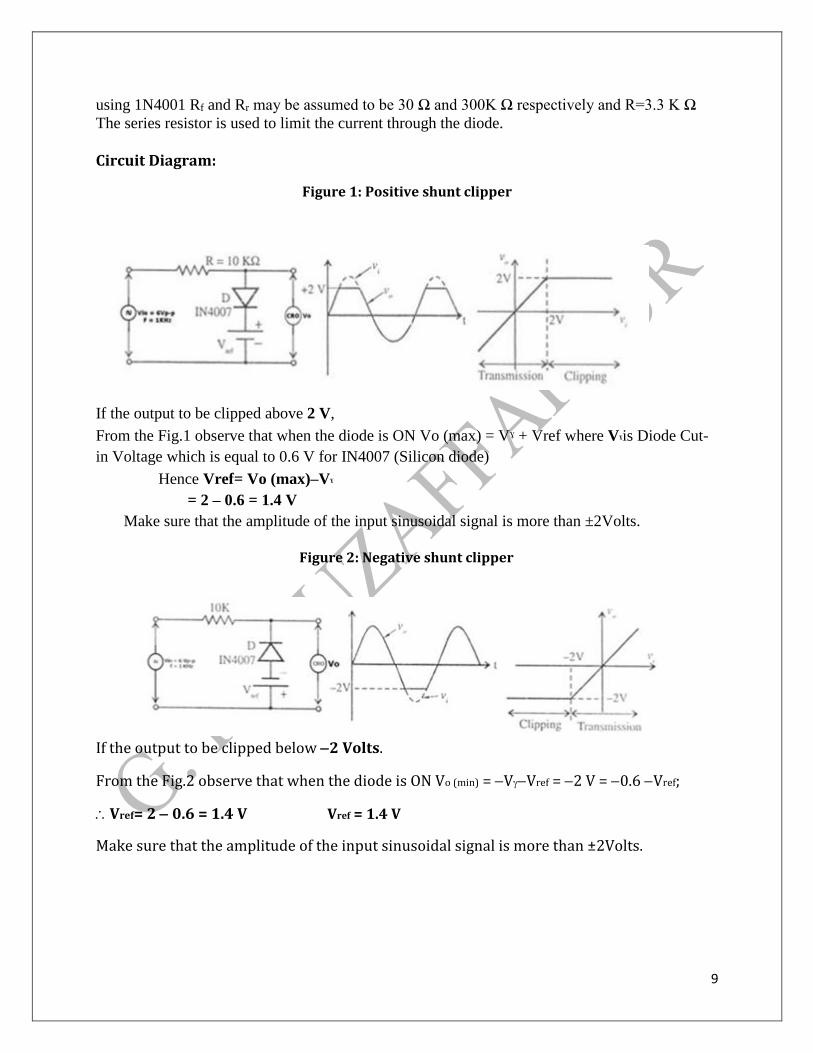
DESIGN: Assume Forward Resistance of Diode, Rf =100 Ω; Reverse Resistance of Diode, Rr =1MΩ The
series resistance is calculated such that R √R f . Rr√100 × 10610K 6 Note: If you are
9
using 1N4001 Rf and Rr may be assumed to be 30 Ω and 300K Ω respectively and R=3.3 K Ω
The series resistor is used to limit the current through the diode.
Circuit Diagram:
Figure 1: Positive shunt clipper
If the output to be clipped above 2 V, From the Fig.1 observe that when the diode is ON Vo (max) = Vˠ + Vref where Vˠis Diode Cut-
in Voltage which is equal to 0.6 V for IN4007 (Silicon diode)
Hence Vref= Vo (max)–Vˠ = 2 – 0.6 = 1.4 V
Make sure that the amplitude of the input sinusoidal signal is more than ±2Volts.
Figure 2: Negative shunt clipper
If the output to be clipped below 2 Volts.
From the Fig.2 observe that when the diode is ON Vo (min) = VVref = 2 V = 0.6 Vref;
Vref= 2 0.6 = 1.4 V Vref = 1.4 V
Make sure that the amplitude of the input sinusoidal signal is more than ±2Volts.
10
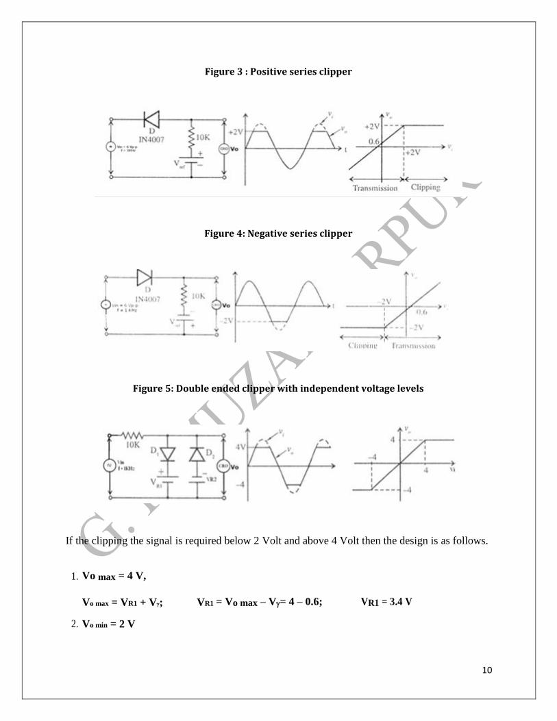
Figure 3 : Positive series clipper
Figure 4: Negative series clipper
Figure 5: Double ended clipper with independent voltage levels
If the clipping the signal is required below 2 Volt and above 4 Volt then the design is as follows.
1. Vo max = 4 V,
Vo max = VR1 + V; VR1 = Vo max – V= 4 – 0.6; VR1 = 3.4 V
2. Vo min = 2 V
11
Vo min = VR2 – V; VR2 = Vo min + V = 2 + 0.6; VR2 = 2.6 V
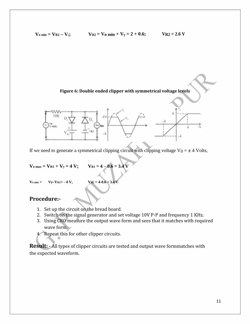
Figure 6: Double ended clipper with symmetrical voltage levels
If we need to generate a symmetrical clipping circuit with clipping voltage V0 = ± 4 Volts,
Vo max = VR1 + V = 4 V; VR1 = 4 – 0.6 = 3.4 V
Vo min = VVR2= - 4 V, VR2 = 4-0.6 = 3.4 V
Procedure:-
1. Set up the circuit on the bread board. 2. Switch on the signal generator and set voltage 10V P-P and frequency 1 KHz. 3. Using CRO measure the output wave form and sees that it matches with required
wave form.
4. Repeat this for other clipper circuits.
Result: - All types of clipper circuits are tested and output wave formmatches with
the expected waveform.
12
Government Polytechnic, Muzaffarpur
Analog Electronics Lab
Subject Code: 1621307
Experiment:4
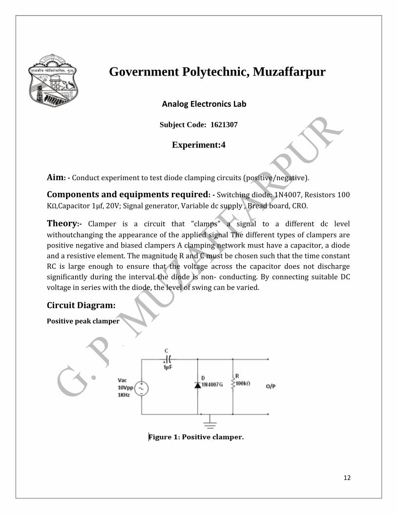
Aim: - Conduct experiment to test diode clamping circuits (positive/negative).
Components and equipments required: - Switching diode: 1N4007, Resistors 100
KΩ,Capacitor 1µf, 20V; Signal generator, Variable dc supply , Bread board, CRO.
Theory:- Clamper is a circuit that "clamps" a signal to a different dc level
withoutchanging the appearance of the applied signal The different types of clampers are
positive negative and biased clampers A clamping network must have a capacitor, a diode
and a resistive element. The magnitude R and C must be chosen such that the time constant
RC is large enough to ensure that the voltage across the capacitor does not discharge
significantly during the interval the diode is non- conducting. By connecting suitable DC
voltage in series with the diode, the level of swing can be varied.
Circuit Diagram:
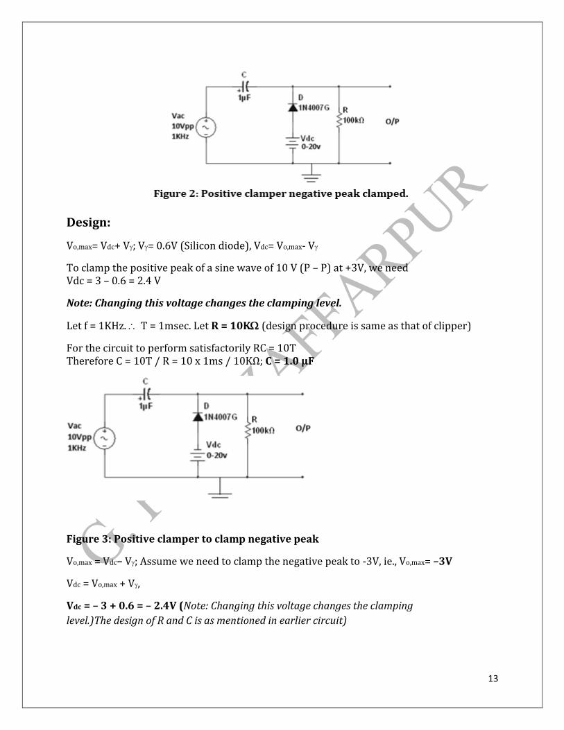
Positive peak clamper
13
Design:
Vo,max= Vdc+ V; V= 0.6V (Silicon diode), Vdc= Vo,max- V
To clamp the positive peak of a sine wave of 10 V (P – P) at +3V, we need Vdc = 3 – 0.6 = 2.4 V
Note: Changing this voltage changes the clamping level.
Let f = 1KHz. T = 1msec. Let R = 10K (design procedure is same as that of clipper)
For the circuit to perform satisfactorily RC = 10T Therefore C = 10T / R = 10 x 1ms / 10KΩ; C = 1.0 µF
Figure 3: Positive clamper to clamp negative peak
Vo,max = Vdc– V; Assume we need to clamp the negative peak to -3V, ie., Vo,max= –3V
Vdc = Vo,max + V,
Vdc = – 3 + 0.6 = – 2.4V (Note: Changing this voltage changes the clamping
level.)The design of R and C is as mentioned in earlier circuit)

14
Procedure:-
5. Set up the circuit on the bread board. 6. Switch on the signal generator and set voltage 10V P-P and frequency 1 KHz. 7. Using CRO measure the output wave form and sees that it matches with required
wave form.
8. Repeat this for other clamper circuits.
Result: - All types of clamper circuits are tested and output wave formmatches with
the expected waveform.
15
Government Polytechnic, Muzaffarpur
Analog Electronics Lab
Subject Code: 1621307
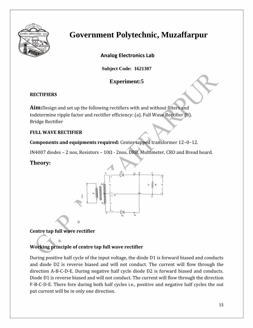
Experiment:5
RECTIFIERS
Aim:Design and set up the following rectifiers with and without filters and
todetermine ripple factor and rectifier efficiency: (a). Full Wave Rectifier (b).
Bridge Rectifier
FULL WAVE RECTIFIER
Components and equipments required: Center tapped transformer 12–0–12.
IN4007 diodes – 2 nos, Resistors – 10Ω - 2nos, DRB, Multimeter, CRO and Bread board.
Theory:
Centre tap full wave rectifier
Working principle of centre tap full wave rectifier
During positive half cycle of the input voltage, the diode D1 is forward biased and conducts
and diode D2 is reverse biased and will not conduct. The current will flow through the
direction A-B-C-D-E. During negative half cycle diode D2 is forward biased and conducts.
Diode D1 is reverse biased and will not conduct. The current will flow through the direction
F-B-C-D-E. There fore during both half cycles i.e., positive and negative half cycles the out
put current will be in only one direction.

16
Full wave bridge rectifier
Working principle of full wave bridge rectifier
During positive half cycle of the input voltage, the diode D1 and D3 is forward biased and
both diodes will conduct and diode D2 and D4 is reverse biased and will not conduct. The
current will flow through the direction A-B-C-D-E-F-G.
During negative half cycle, the diode D2 and D4 is forward biased and both diodes will
conduct and diode D1 and D3 is reverse biased and will not conduct. he current will flow
through the direction G-F-C-D-E-B-A. There fore during both half cycles i.e., positive and
negative half cycles the out put current will be in only one direction i.e., from point C to D.
Design: (Common for both rectifiers)
For the transformer, primary voltage VP=230 V
Secondary voltage VS=12V
Voltage across diode VD = 0.6 V (Silicon transistor)
For a diode current of 10mA, i.e., ID = 10mA
RL = [VS – VD]/ ID = [12 - 0.6] / 10mA = 1.14 KΩ ; choose RL = 1 KΩ
With capacitor filter, ripple factor
Allowing 3% ripple, i.e., r=0.03, f = 50 Hz, RL = 1 KΩ we get C = 96.225µF, let C=100 µF Vm
= 12×2 = 16.97 V (Maximum value of the sinusoidal voltage applied to the rectifier)Vdc =
2Vm/π = 10.8V (For the rectifier without filter, Theoretical)
Idc = Vdc/RL(DC Current through the load)

17
Idc = 10.8V/47 = 229.78 mA (Full Load current, min value of RLshown in the Table,with RS= Rf =0),
Pdc= Vdc2/RL(Load Power)
Pac= VS×IS(Power supplied by the transformer)
Ripple factor γ = Vac/Vdc (=1.21 Theoretical)
%Efficiency = Pdc/Pac ((40.6%, Theoretical)
%Regulation = E = (VNL-VFL)/VFL
Circuit Diagram:
1. Center tap full wave rectifier with filter (remove C for rectifier without
filter)
2. Full wave bridge rectifier with filter (remove C for rectifier without filter)
18
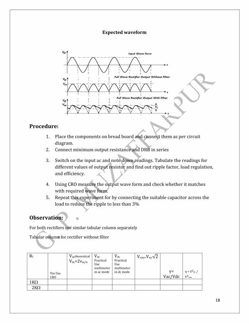
Expected waveform
Procedure:
1. Place the components on bread board and connect them as per circuit
diagram.
2. Connect minimum output resistance and DRB in series
3. Switch on the input ac and note down readings. Tabulate the readings for
different values of output resistor and find out ripple factor, load regulation,
and efficiency.
4. Using CRO measure the output wave form and check whether it matches
with required wave form.
5. Repeat this experiment for by connecting the suitable capacitor across the
load to reduce the ripple to less than 3%
Observation:
For both rectifiers use similar tabular column separately
Tabular column for rectifier without filter
RL
Vm Use CRO
Vdctheoretical
Vdc=2vm/π Vdc Practical Use multimeter in ac mode
Vdc Practical Use multimeter in dc mode
Vrms=Vm/√2
γ= Vac/Vdc
η = V2dc /
V2rms
1K
2K
19
3 KΩ
4 KΩ
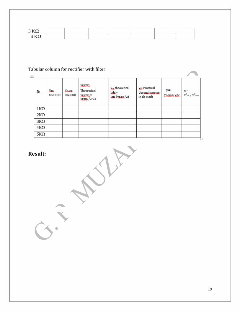
Tabular column for rectifier with filter
Result:

20
Government Polytechnic, Muzaffarpur
Analog Electronics Lab
Subject Code: 1621307
Experiment:6
CLASS B PUSH PULL AMPLIFIER
Aim: Testing of a transformer less class-B push pull power amplifier and determinationof its conversion efficiency.
Components and equipments required: Complementary symmetry transistors
SL100and SK100, Resistors – 47KΩ - 2nos, 4.7KΩ - 1no, 1KΩ - 2nos, 10KΩ pot - 1no,0.01µF
– 2 nos, Load box or DRB, Multimeter, Connecting wires and Bread board/Spring board
with spring terminals.
Theory: Complementary-Symmetry Class B Amplifier uses complementary or
matchingpairs of power transistors. The Class B amplifier circuit uses complimentary
transistors for each half of the waveform. Main disadvantage of class B type push-pull
amplifiers is that they suffer from an effect known commonly as Crossover Distortion.
Transistor takes approximately 0.7 volts (measured from base to emitter) to get a bipolar
transistor to start conducting. In a pure class B amplifier, the output transistors are not
"pre-biased" to an "ON" state of operation. Hence part of the output waveform which falls
below this 0.7 volt window will not be reproduced accurately as the transition between the
two transistors. The output transistors for each half of the waveform (positive and
negative) will each have a 0.7 volt area in which they will not be conducting resulting in
both transistors being "OFF" at the same time.
Illustrating Cross-over distortion
21
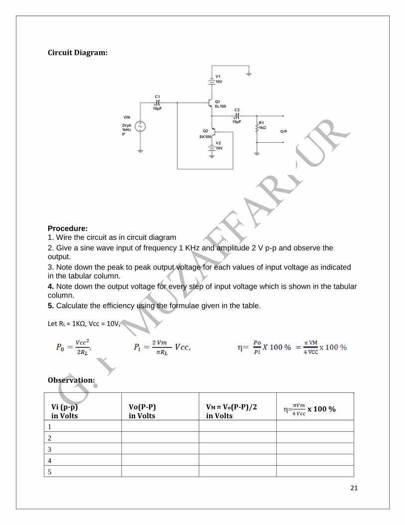
Circuit Diagram:
Procedure: 1. Wire the circuit as in circuit diagram
2. Give a sine wave input of frequency 1 KHz and amplitude 2 V p-p and observe the output.
3. Note down the peak to peak output voltage for each values of input voltage as indicated in the tabular column.
4. Note down the output voltage for every step of input voltage which is shown in the tabular column.
5. Calculate the efficiency using the formulae given in the table. Let RL = 1KΩ, Vcc = 10V,
Observation:
Vi (p-p) in Volts
Vo(P-P) in Volts
VM = Vo(P-P)/2 in Volts
𝜋𝑉𝑚
4 𝑉𝑐𝑐x 100 %
1
2
3
4
5

22
6
7
Result:
23
Government Polytechnic, Muzaffarpur
Analog Electronics Lab
Subject Code: 1621307
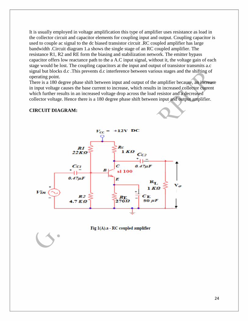
Experiment:7
RC coupled single stage BJT amplifier AIM:
Wiring of RC coupled single stage BJT amplifier and determination of the gainfrequency
response, input and output impedances.
COMPONENTS REQUIRED:
THEORY:
Amplifier circuit is used to enhance or amplify the input signal level. RC coupled amplifier is
most popular type of coupling because it provides excellent audio fidelity over wide range of
frequencies. Coupling is used to couple alternative input & output signal with DC biased
transistor device or any other device used for amplification.
24
It is usually employed in voltage amplification this type of amplifier uses resistance as load in
the collector circuit and capacitor elements for coupling input and output. Coupling capacitor is
used to couple ac signal to the dc biased transistor circuit .RC coupled amplifier has large
bandwidth .Circuit diagram 1.a shows the single stage of an RC coupled amplifier. The
resistance R1, R2 and RE form the biasing and stabilization network. The emitter bypass
capacitor offers low reactance path to the a A.C input signal, without it, the voltage gain of each
stage would be lost. The coupling capacitors at the input and output of transistor transmits a.c
signal but blocks d.c .This prevents d.c interference between various stages and the shifting of
operating point.
There is a 180 degree phase shift between input and output of the amplifier because, an increase
in input voltage causes the base current to increase, which results in increased collector current
which further results in an increased voltage drop across the load resistor and a decreased
collector voltage. Hence there is a 180 degree phase shift between input and output amplifier.
CIRCUIT DIAGRAM:
25
DESIGN:
Given:
Vcc=12 V, Ic =4.5 mA, β=100 (for SL 100)
Assume VRE =VE=VCC/10=12/10=1.2 V
To find RE :
RE=1.2/Ic=1.2/4.5m
=0.267 K ohm
RE=270Ω
To find Rc: Choose VCE=Vcc/2 =12/2=6 V
Apply KVL in CE loop:
Vcc-(IcRc)- VCE- VRE=0
12-(4.5Rc)-6-1.2=0
Rc=1.07 K ohm

26
RC=1 K Ω
To find R1 & R2:
VB = VBE + VRE
VB =0.7+1.2=1.9V
Ic=β IB
IB = Ic/ β =4.5m/100=0.045mA
Assume 10IB flows through R1 and 9IB flows through R2
R1= Vcc -VB/10 IB=22.7
Use R1=22KΩ
R2= VB/9IB =4.69KΩ
Use R2=4.7KΩ
To find CE
Let fL=500Hz ( Lower Cut-off frequency )
fL= 1 / 2π*Re*CE
But Re ≈ re Here re=VT / Ic =26mV/4.5mA=5.77Ω
Re ≈ re ≈6Ω
1/(2π*fL* CE )= Re
Therefore, CE=1/(2*π*500*6)
CE =53 μF
Use CE ≈50 μF
To design Cc1 fL= 1 / (2π*(Ri/10)*Cc1)
Ri= R1 || R2 || hie Where hie=β*re
For SL100 β=150 and Let re=10Ω , hie=150*10=1.5KΩ
Ri≈hie=1.5KΩ
27
So Cc1= 1 / 2π*Ri*fL= 1 / (2π*0.15KΩ*500) =2.12 uF
To design Cc2 Let RL=1KΩ
fL= 1 / (2π*((Ro + RL)/10)*Cc2)
For the above circuit Ro=Rc=1KΩ and let RL=1KΩ
So Cc2= 1 / (2π*0.2KΩ*500)= 1.59 uF
Use Cc1 = Cc2=0.47 μF (ceramic) PROCEDURE Rig up the circuit as shown in the circuit diagram in Fig 1(A).b without connecting signal generator.
Check the biasing conditions i.e. VCC =12V and check corresponding values of VCE,VBE,VE.
1. Connect the as in Fig 1(A).a with signal generator and designed capacitor values and set the input voltage constant at 50mV(p-p) , 1KHz.
2. Now vary the input frequency starting from 100Hz to MHz range and note the corresponding output voltage(peak to peak).
3. Plot the graph of frequency v/s output voltage gain in decibel with frequency on X-axis and dB
gain on Y-axis and determine the bandwidth.
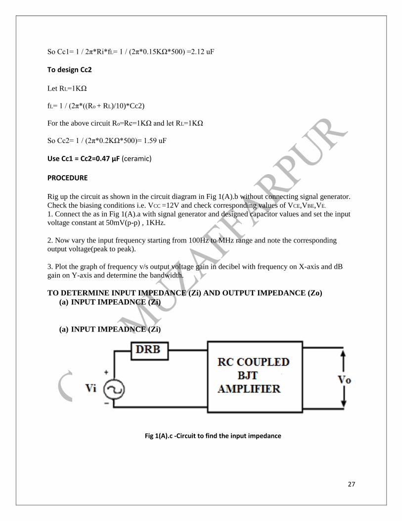
TO DETERMINE INPUT IMPEDANCE (Zi) AND OUTPUT IMPEDANCE (Zo)
(a) INPUT IMPEADNCE (Zi)
(a) INPUT IMPEADNCE (Zi)
Fig 1(A).c -Circuit to find the input impedance
28
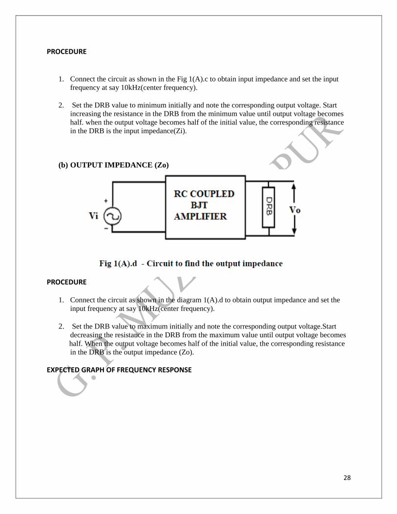
PROCEDURE
1. Connect the circuit as shown in the Fig 1(A).c to obtain input impedance and set the input
frequency at say 10kHz(center frequency).
2. Set the DRB value to minimum initially and note the corresponding output voltage. Start
increasing the resistance in the DRB from the minimum value until output voltage becomes
half. when the output voltage becomes half of the initial value, the corresponding resistance
in the DRB is the input impedance(Zi).
(b) OUTPUT IMPEDANCE (Zo)
PROCEDURE
1. Connect the circuit as shown in the diagram 1(A).d to obtain output impedance and set the
input frequency at say 10kHz(center frequency).
2. Set the DRB value to maximum initially and note the corresponding output voltage.Start
decreasing the resistance in the DRB from the maximum value until output voltage becomes half. When the output voltage becomes half of the initial value, the corresponding resistance
in the DRB is the output impedance (Zo).
EXPECTED GRAPH OF FREQUENCY RESPONSE
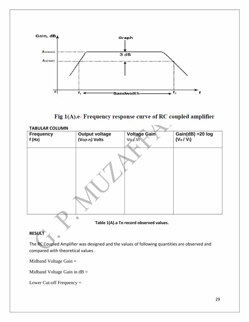
29
TABULAR COLUMN Frequency f (Hz)
Output voltage (VO(P-P)) Volts
Voltage Gain Vo / Vi
Gain(dB) =20 log (Vo / Vi)
Table 1(A).a To record observed values.
RESULT
The RC Coupled Amplifier was designed and the values of following quantities are observed and
compared with theoretical values .
Midband Voltage Gain =
Midband Voltage Gain in dB =
Lower Cut-off Frequency =

30
Upper Cut-off Frequency =
Bandwidth (BW) =
Input Resistance (Zi) =
Output Resistance (Zo) =
31
Government Polytechnic, Muzaffarpur
Analog Electronics Lab
Subject Code: 1621307
Experiment :8
RC PHASE SHIFT OSCILLATOR AIM: To design and verify the performance of RC phase shift Oscillator for the given frequency EQUIPMENTS REQUIRED:
THEORY: RC phase shift Oscillator basically consists of an amplifier and feed back network consisting of resistors and capacitors in ladder fashion. The basic RC circuit is as shown below

32
Fig 3.a Phase lead network and Phasor diagram
The current I is in phase with Vo, whereas the capacitor voltage Vc lags the current I by φ (90®→Ideal value). OR the output voltage Vo leads the I/P voltage Vi by angle φ is adjusted in practice, equal to 60®.RC network is used in feedback path. In Oscillator, feedback network must introduce a phase shift of180® to obtain total phase shift around a loop as 360®.Thus three Rc network each provide 60® phase shift is cascaded, so that it produces total 180® phase shift. The Oscillator circuit consisting amplifier and Rc feedback network is as shown below.
CIRCUIT DIAGRAM:
fig 3.b Circuit diagram of Phase Shift Oscillator
33
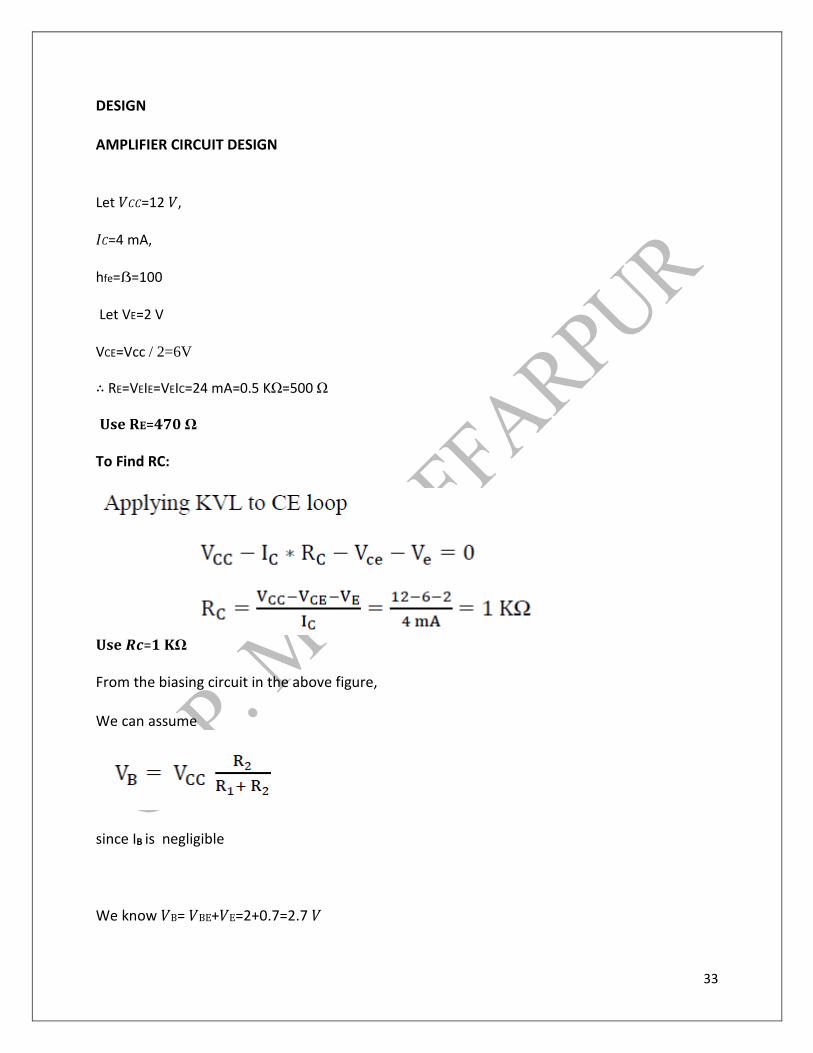
DESIGN AMPLIFIER CIRCUIT DESIGN Let 𝑉𝐶𝐶=12 𝑉, 𝐼𝐶=4 mA, hfe=ẞ=100 Let VE=2 V VCE=Vcc / 2=6V
∴ RE=VEIE=VEIC=24 mA=0.5 KΩ=500 Ω
𝐔𝐬𝐞 𝐑𝐄=𝟒𝟕𝟎 Ω
To Find RC:
𝐔𝐬𝐞 𝑹𝒄=𝟏 𝐊Ω
From the biasing circuit in the above figure, We can assume
since IB is negligible
We know 𝑉B= 𝑉BE+𝑉E=2+0.7=2.7 𝑉

34
0.225 R1+ 0.225 R2=R2
0.225 R1=0.775 R2 R1=3.44 R2
𝐒𝐚𝐲 𝐢𝐟 𝐑𝟐=𝟔.𝟖 𝐊Ω
then R1=23.3 KΩ
,𝐔𝐬𝐞 𝐑𝟏=𝟐𝟐 𝐊Ω
To Design CE
To design Cc

35
DESIGN OF PHASE-SHIFTING NETWORK The frequency of Oscillations is determined by phase shifting network. The Oscillating frequency for the above circuit is given by
where K= RC/R which is usually<1 𝐋𝐞𝐭 𝐟=𝟐 𝐊𝐇𝐳 (𝐀𝐮𝐝𝐢𝐨 𝐟𝐫𝐞𝐪𝐮𝐞𝐧𝐜𝐲 𝐫𝐚𝐧𝐠𝐞 𝟐𝟎 𝐇𝐳 𝐭𝐨 𝟐𝟎 𝐊𝐇𝐳)
and 𝐑=𝟐.𝟐 𝐊Ω
C=0.0129 uF Use C=0.01uF PROCEDURE
Make the circuit connections as shown in Fig 3.b
The output Vo is obtained on CRO. The 10 KΩ pot is adjusted to get a stable output on the
CRO.
The frequency of Oscillations is measured using CRO and then compared with the theoretical
values.
With respect to output at point P, the waveforms at point Q, R and S are observed on the CRO.
We can see the phase shift at each point being 600, 1200 and 1800 respectively.
NOTE:
The value of all three capacitors C is changed and the frequency of Oscillation can be changed to
new value and is measured again.
Designed frequency 2 KHZ
Actual frequency got 2KHZ
Phase shift between P & Q 60

36
P & R 120
P & S 180
RESULTS :
Theoretical frequency of oscillations = KHz
Practical frequency of oscillations = KHz

37
Government Polytechnic, Muzaffarpur
Analog Electronics Lab
Subject Code: 1621307
Experiment :9A
BJT HARTELY OSCILLATOR AIM:
Testing for the performance of BJT-Hatley for RF range fo ≥ 100KHz.
COMPONENTS REQUIRED:
THEORY If the oscillator uses two inductors and one capacitor in the feedback (or Tank) circuit, then it is called as Hartley oscillator.
38
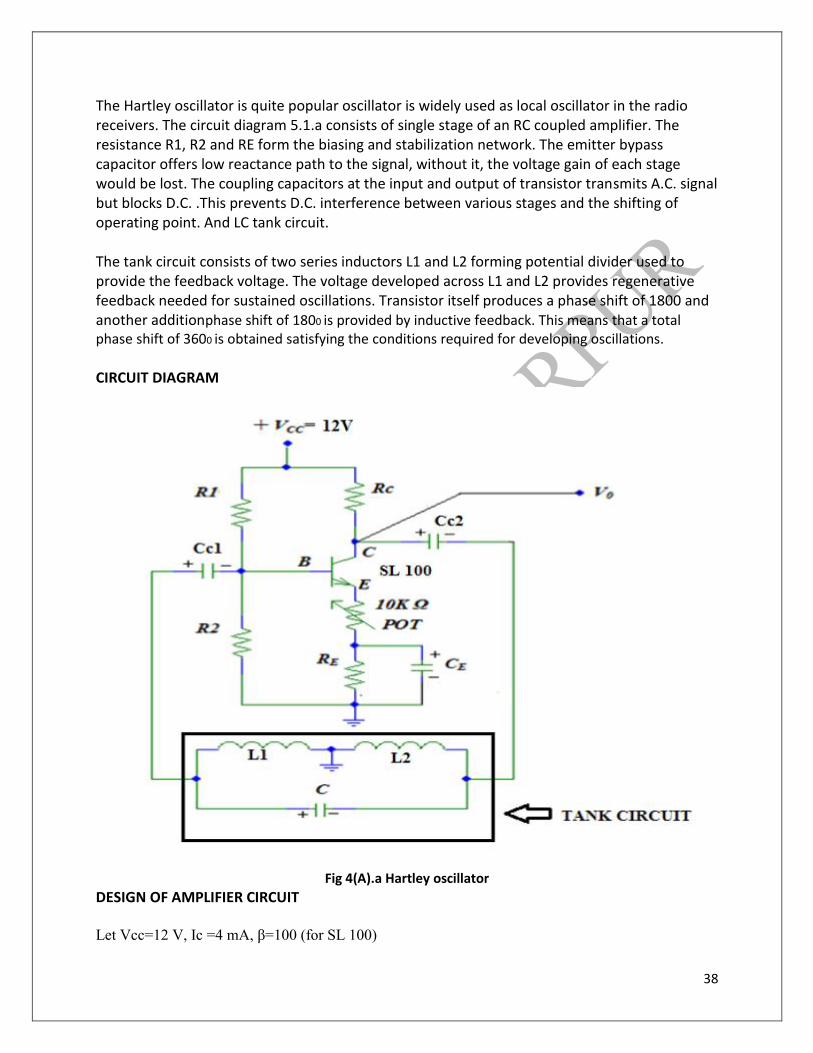
The Hartley oscillator is quite popular oscillator is widely used as local oscillator in the radio receivers. The circuit diagram 5.1.a consists of single stage of an RC coupled amplifier. The resistance R1, R2 and RE form the biasing and stabilization network. The emitter bypass capacitor offers low reactance path to the signal, without it, the voltage gain of each stage would be lost. The coupling capacitors at the input and output of transistor transmits A.C. signal but blocks D.C. .This prevents D.C. interference between various stages and the shifting of operating point. And LC tank circuit. The tank circuit consists of two series inductors L1 and L2 forming potential divider used to provide the feedback voltage. The voltage developed across L1 and L2 provides regenerative feedback needed for sustained oscillations. Transistor itself produces a phase shift of 1800 and another additionphase shift of 1800 is provided by inductive feedback. This means that a total phase shift of 3600 is obtained satisfying the conditions required for developing oscillations.
CIRCUIT DIAGRAM
Fig 4(A).a Hartley oscillator
DESIGN OF AMPLIFIER CIRCUIT Let Vcc=12 V, Ic =4 mA, β=100 (for SL 100)

39
As usual we can assume VRE = VE= Vcc/10=10/10=1.2 V
To find RE : VE=IERE =1.2 V
RE = VE / IE
= VE / Ic (as IE ≈ Ic)
=1.2V/4mA
=500Ω
use RE =470Ω (standard) in series with 1KΩ pot (to provide gain control) To find Rc: Let VCE =Vcc/2 ( Q point in middle of active region)
=12/2= 6V
Apply KVL in CE loop:
VCC-ICRC- VCE - IERE =0
12-(4m*RC)-5-1=0
Rc=1KΩ To find R1 & R2: Let a current of 10IB flows through R1 and 9IB flows through R2
VB = VBE+ VRE
VB =0.7+1.2=1.9V
Ic=β IB
IB = Ic/ β =4m/100=40μA
R1= Vcc -VB/10 IB=( 12-1.9)/(40*10-6*10)=23 KΩ
Use R1 =22KΩ
R2= VB/9IB = 2.7/(9*40*10-6)=7.5KΩ
Use R2=6.8KΩ

40
To design CE
Let fL=500Hz ( Lower Cut-off frequency )
fL= 1 / 2π*Re*CE
But Re ≈ re
Here re=VT / Ic =26mV/4mA=6.5Ω
Re ≈ re ≈6.5Ω
1/(2π*fL* CE )= Re =>
Therefore, CE=1/(2*π*500*6.5)
CE =49 μF
Use CE ≈50 μF or 10 μF
To design Cc1 fL= 1 / (2π*(Ri/10)*Cc1)
Ri= R1 || R2 || hie
Where hie=β*re
For SL100 β=150 and re=6.5Ω ,
hie=150*6.5≈1KΩ
Ri≈hie=1KΩ
So Cc1= 1 / 2π*Ri*fL= 1 / (2π*(1KΩ/10)*500) =3.18 uF
Use Cc1 =3 μF or 0.47 μF . To design Cc2 Let RL=1KΩ
fL= 1 / (2π*((Ro + RL)/10)*Cc2)
For the above circuit Ro=Rc=1KΩ and
let RL=1KΩ
So Cc2= 1 / (2π*0.2KΩ*500)= 1.59 uF

41
Let RL=1KΩ
fL= 1 / (2π*((Ro + RL)/10)*Cc2)
For the above circuit Ro=Rc=1KΩ and
let RL=1KΩ
So Cc2= 1 / (2π*0.2KΩ*500)= 1.59 uF
Use Cc1 = Cc2=2 μF or 0.47uF(ceramic)
TANK CIRCUIT DESIGN Given f =100KHz
f = 1 / 2π√ Leq C
Let Leq= L1 + L2 = 2mH
Use L1=L2=1mH
C = 1 / (4π2 * 2mH * f 2)
C = 0.0012μF
Use C=0.001uF
PROCEDURE
1. Rig up the circuit diagram as shown in the circuit diagram without the tank circuit and check
the biasing conditions with Vcc=12V i.e. check VCE,VBE and VE.
2. Connect the tank circuit and vary the 10K pot to get proper sine wave across the output
terminals and check the frequency of output waveform and compare it with the theoretical
value and tabulate the readings .
EXPECTED OUTPUT WAVEFORM
42
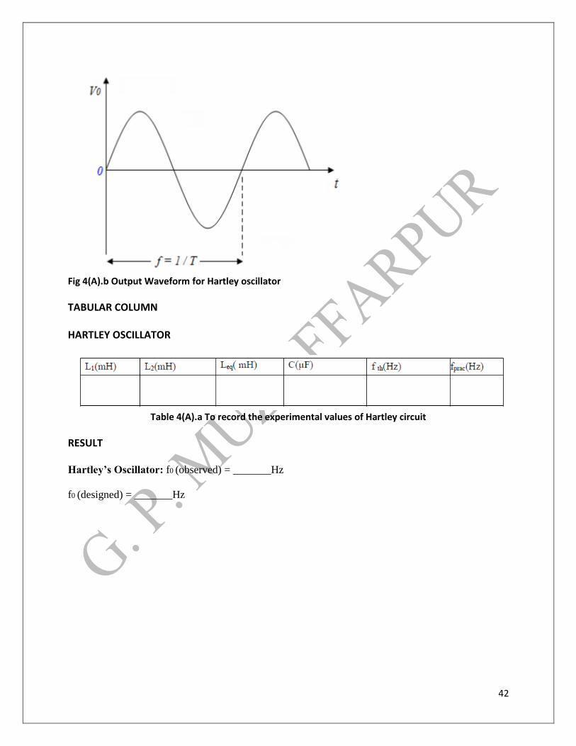
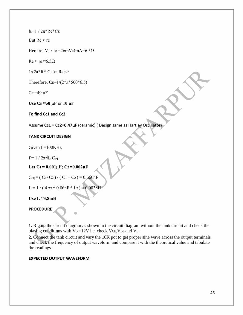
Fig 4(A).b Output Waveform for Hartley oscillator
TABULAR COLUMN HARTLEY OSCILLATOR
Table 4(A).a To record the experimental values of Hartley circuit
RESULT Hartley’s Oscillator: f0 (observed) = _______Hz
f0 (designed) = _______Hz
43
Government Polytechnic, Muzaffarpur
Analog Electronics Lab
Subject Code: 1621307
Experiment :9 B
BJT COLPITTS OSCILLATOR
AIM: Testing for the performance of BJT- colpitts oscillators for RF range fo ≥100KHz. COMPONENTS REQUIRED:
44
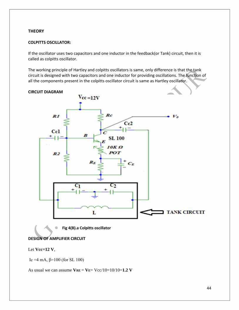
THEORY COLPITTS OSCILLATOR: If the oscillator uses two capacitors and one inductor in the feedback(or Tank) circuit, then it is called as colpitts oscillator. The working principle of Hartley and colpitts oscillators is same, only difference is that the tank circuit is designed with two capacitors and one inductor for providing oscillations. The function of all the components present in the colpitts oscillator circuit is same as Hartley oscillator. CIRCUIT DIAGRAM
Fig 4(B).a Colpitts oscillator
DESIGN OF AMPLIFIER CIRCUIT Let Vcc=12 V,
Ic =4 mA, β=100 (for SL 100)
As usual we can assume VRE = VE= Vcc/10=10/10=1.2 V

45
To find RE : VE=IERE =1.2 V
RE = VE / IE
= VE / Ic (as IE ≈ Ic)
=1.2V/4mA=500Ω
Use RE =470Ω (standard) in series with 1KΩ pot (to provide gain control) To find Rc: Let VCE =Vcc/2 ( Q point in middle of active region)
=12/2= 6V
Apply KVL in CE loop:
VCC-ICRC- VCE - IERE =0
12-(4m*RC)-5-1=0
Rc=1KΩ
To find R1 & R2: Let a current of 10IB flows through R1 and 9IB flows through R2
VB = VBE + VRE
VB =0.7+1.2=1.9V
Ic=β IB
IB = Ic/ β =4m/100=40μA
R1= Vcc -VB/10 IB=( 12-1.9)/(40*10-6*10)=23 KΩ
Use R1 =22KΩ
R2= VB/9IB = 2.7/(9*40*10-6)=7.5KΩ
Use R2=6.8KΩ
To find CE
Let fL=500Hz ( Lower Cut-off frequency )
46
fL= 1 / 2π*Re*CE
But Re ≈ re
Here re=VT / Ic =26mV/4mA=6.5Ω
Re ≈ re ≈6.5Ω
1/(2π*fL* CE )= Re =>
Therefore, CE=1/(2*π*500*6.5)
CE =49 μF
Use CE ≈50 μF or 10 μF
To find Cc1 and Cc2 Assume Cc1 = Cc2=0.47μF (ceramic) ( Design same as Hartley Oscillator) TANK CIRCUIT DESIGN Given f =100KHz
f = 1 / 2π√L Ceq
Let C1 = 0.001μF; C2 =0.002μF
Ceq = ( C1* C2 ) / ( C1 + C2 ) = 0.666nF
L = 1 / ( 4 π2 * 0.66nF * f 2 ) ≈ 0.0038H
Use L ≈3.8mH
PROCEDURE 1. Rig up the circuit diagram as shown in the circuit diagram without the tank circuit and check the
biasing conditions with Vcc=12V i.e. check VCE,VBE and VE.
2. Connect the tank circuit and vary the 10K pot to get proper sine wave across the output terminals
and check the frequency of output waveform and compare it with the theoretical value and tabulate
the readings
EXPECTED OUTPUT WAVEFORM
47
Fig 4(B).b Output Waveform for Hartley oscillator
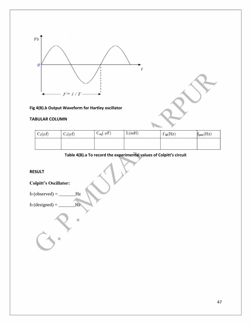
TABULAR COLUMN
Table 4(B).a To record the experimental values of Colpitt’s circuit
RESULT Colpitt’s Oscillator:
f0 (observed) = _______Hz
f0 (designed) = _______Hz
48
Government Polytechnic, Muzaffarpur
Analog Electronics Lab
Subject Code: 1621307
Experiment :10
BJT CRYSTAL OSCILLATOR AIM
Testing for the performance of BJT-crystal oscillators for fo ≥ 100KHz COMPONENTS REQUIRED
THEORY

49
Crystal oscillators are made from quartz. A crystal can be operated in the series resonant or parallel resonant mode. In the series mode crystal offers minimum impedance at resonance and in parallel mode it offers maximum impedance and is inductive. Since the parallel resonant frequency of a crystal is slightly higher than its series resonant frequency, the method of connection is important. In this experiment we will construct oscillators by connecting the crystal in the parallel resonant mode. But both oscillator’s exhibit good stability, but the sine wave outputs may be slightly distorted. In transistor crystal oscillator, note that it is a colpitt’s oscillator modified to acts as a crystal oscillator the only change in the addition of the crystal in the feedback network. The crystal will act as a parallel tuned circuit, as you can see in this circuit 6.6 that instead of resonance caused by L and C. We have the parallel resonance of the crystal at parallel resonance the impedance of the crystal is maximum this means that there is a maximum voltage drops across crystal this in turn will allow the maximum energy through the transistor feedback network at resonance frequency. We note that feedback is positive and phase shift in 1800 is produced by the transistor a further phase shift of 1800 is produced by the capacitor voltage divider this oscillator will oscillate only at resonance frequency even the smallest deviation from resonance frequency will cause the oscillator be acts as an ineffective short consequently we have an extremely stable oscillator. Advantages: 1. They have an order of frequency stability.
2. The quality factor of the crystal is very high.
Disadvantages: 1. They have fragile and consequently can only be used in low power circuit.
2. The frequency of oscillations cannot be changed appreciably.
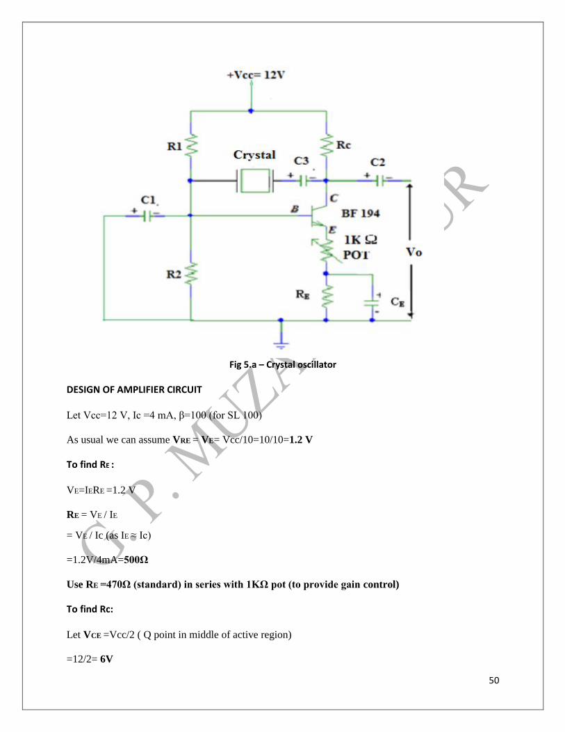
CIRCUIT DIAGRAM
50
Fig 5.a – Crystal oscillator
DESIGN OF AMPLIFIER CIRCUIT Let Vcc=12 V, Ic =4 mA, β=100 (for SL 100)
As usual we can assume VRE = VE= Vcc/10=10/10=1.2 V
To find RE : VE=IERE =1.2 V
RE = VE / IE
= VE / Ic (as IE ≈ Ic)
=1.2V/4mA=500Ω
Use RE =470Ω (standard) in series with 1KΩ pot (to provide gain control)
To find Rc: Let VCE =Vcc/2 ( Q point in middle of active region)
=12/2= 6V
51
Apply KVL in CE loop:
VCC-ICRC- VCE - IERE =0
12-(4m*RC)-5-1=0
Rc=1KΩ
To find R1 & R2: Let a current of 10IB flows through R1 and 9IB flows through R2
VB = VBE+ VRE
VB =0.7+1.2=1.9V
Ic=β IB
IB = Ic/ β =4m/100=40μA
R1= Vcc -VB/10 IB=( 12-1.9)/(40*10-6*10)=23 KΩ
Use R1 =22KΩ
R2= VB/9IB = 2.7/(9*40*10-6)=7.5KΩ
Use R2=6.8KΩ
To find CE
Let fL=500Hz ( Lower Cut-off frequency )
fL= 1 / 2π*Re*CE
But Re ≈ re Here re=VT / Ic =26mV/4mA=6.5Ω
Re ≈ re ≈6.5Ω
1/(2π*fL* CE )= Re =>
Therefore, CE=1/(2*π*500*6.5)
CE =49 μF
Use CE ≈50 μF or 10 μF
Use C1 and C2 0.01 uF each and C3=0.1 uF .
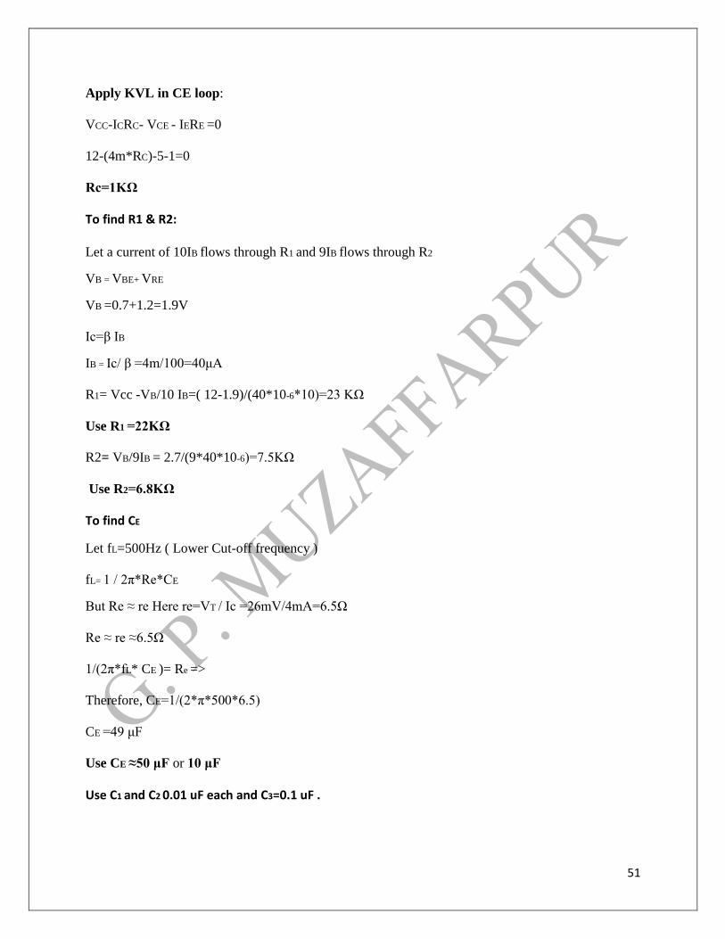
52
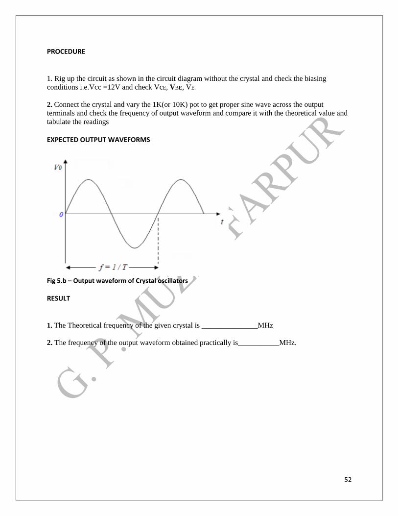
PROCEDURE 1. Rig up the circuit as shown in the circuit diagram without the crystal and check the biasing
conditions i.e.Vcc =12V and check VcE, VBE, VE.
2. Connect the crystal and vary the 1K(or 10K) pot to get proper sine wave across the output
terminals and check the frequency of output waveform and compare it with the theoretical value and
tabulate the readings
EXPECTED OUTPUT WAVEFORMS
Fig 5.b – Output waveform of Crystal oscillators
RESULT 1. The Theoretical frequency of the given crystal is _______________MHz
2. The frequency of the output waveform obtained practically is___________MHz.

53
Government Polytechnic, Muzaffarpur
Analog Electronics Lab
Subject Code: 1621307
Experiment :11
THEVENIN’S AND MAXIMUM POWER TRANSFER THEOREM
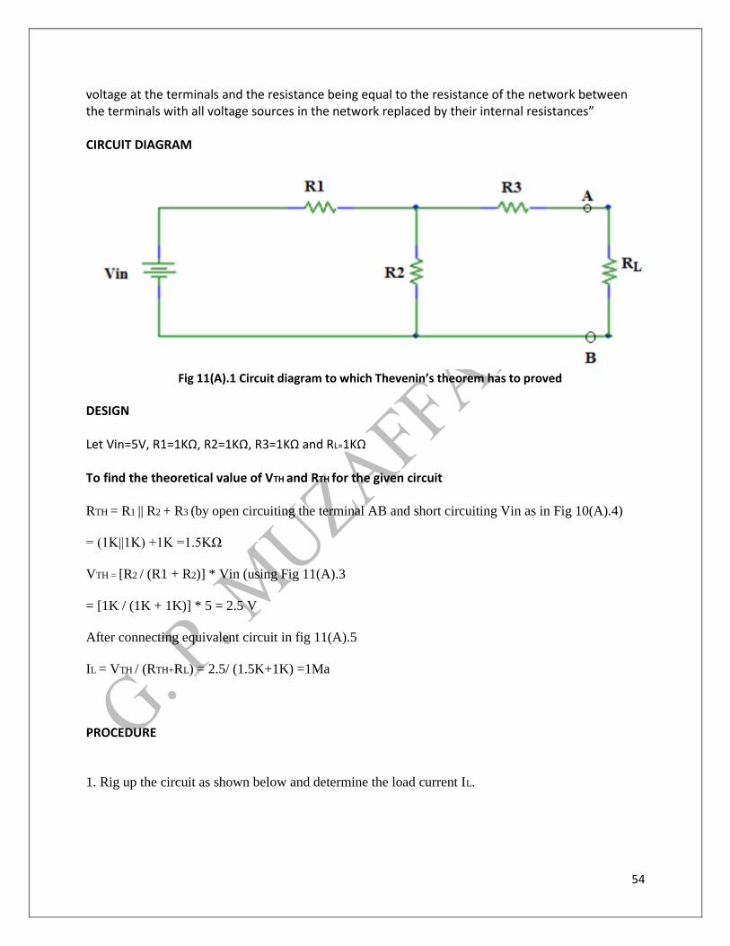
11(A) THEVENIN’S THEOREM
AIM Verification of Thevinin’s Theorem and maximum power transfer therem for DC circuit. COMPONENTS REQUIRED
THEORY THEVENIN’S THEOREY: “Any active linear network with two terminals can be replaced by an equivalent voltage source in series with a resistance, the voltage being equal to the open-circuit
54
voltage at the terminals and the resistance being equal to the resistance of the network between the terminals with all voltage sources in the network replaced by their internal resistances” CIRCUIT DIAGRAM
Fig 11(A).1 Circuit diagram to which Thevenin’s theorem has to proved
DESIGN Let Vin=5V, R1=1KΩ, R2=1KΩ, R3=1KΩ and RL=1KΩ To find the theoretical value of VTH and RTH for the given circuit RTH = R1 || R2 + R3 (by open circuiting the terminal AB and short circuiting Vin as in Fig 10(A).4)
= (1K||1K) +1K =1.5KΩ
VTH = [R2 / (R1 + R2)] * Vin (using Fig 11(A).3
= [1K / (1K + 1K)] * 5 = 2.5 V
After connecting equivalent circuit in fig 11(A).5
IL = VTH / (RTH+RL) = 2.5/ (1.5K+1K) =1Ma
PROCEDURE 1. Rig up the circuit as shown below and determine the load current IL.
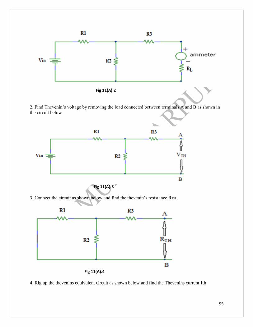
55
Fig 11(A).2
2. Find Thevenin’s voltage by removing the load connected between terminals A and B as shown in
the circuit below
Fig 11(A).3
3. Connect the circuit as shown below and find the thevenin’s resistance RTH .
Fig 11(A).4
4. Rig up the thevenins equivalent circuit as shown below and find the Thevenins current Ith
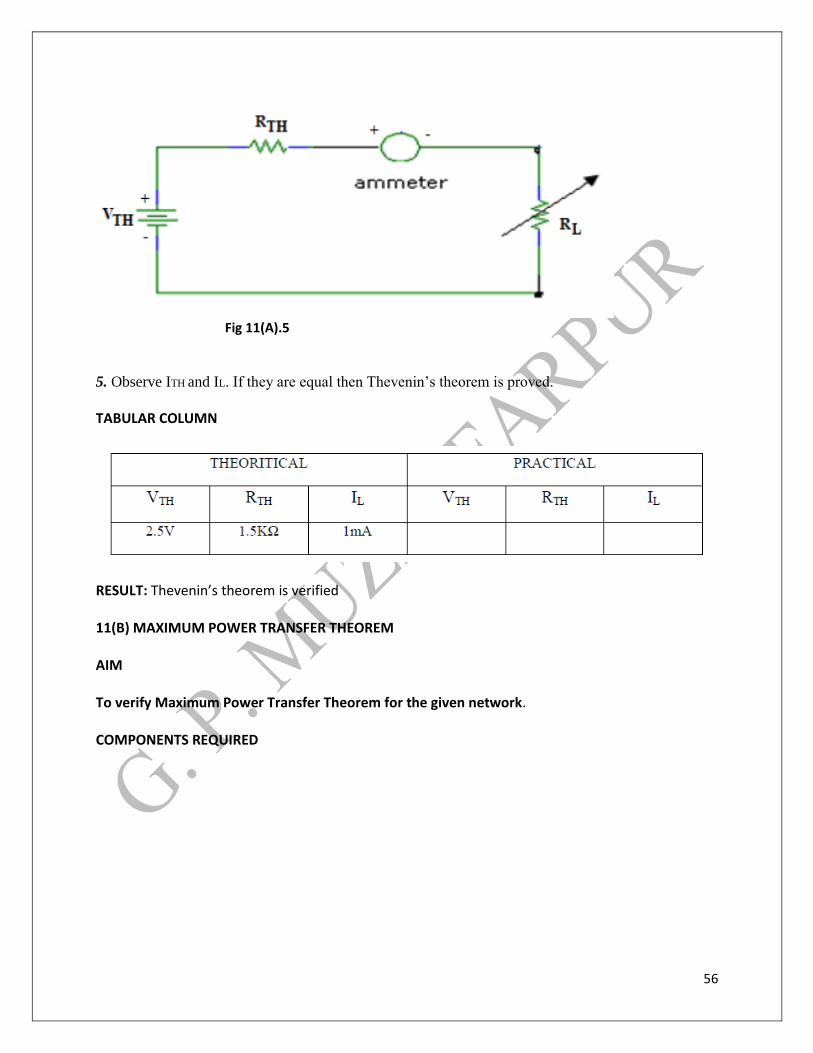
56
Fig 11(A).5
5. Observe ITH and IL. If they are equal then Thevenin’s theorem is proved.
TABULAR COLUMN
RESULT: Thevenin’s theorem is verified 11(B) MAXIMUM POWER TRANSFER THEOREM AIM To verify Maximum Power Transfer Theorem for the given network. COMPONENTS REQUIRED

57
THEORY MAXIMUM POWER TRANSFER THEOREM: “The power derived by an active network to a load connected across its terminal is maximum, when the impedance of the load is the complex conjugate of the active network impedance” The magnitude of maximum power transferred is given by , P = IL2*RL (we have taken a pure resistive circuit to verify the theorem) = [Vth/(RL+Rth)2]*RL
Where the Vth and Rth are the Thevenin’s Voltage and Resistance found looking back into the network (given circuit) from load by open circuiting load. Now P= [Vth/(RL+RL)2]*RL since for maximum power transfer Rth=RL
CIRCUIT DIAGRAM
58
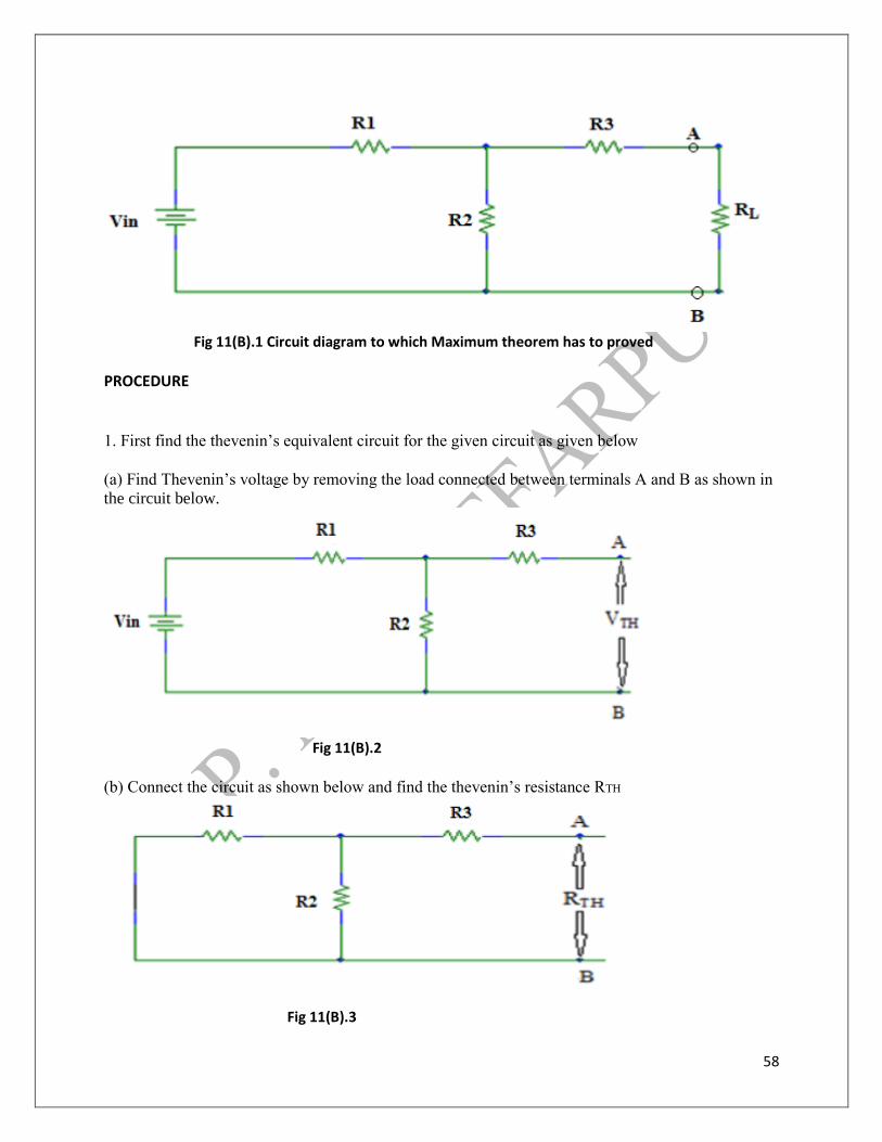
Fig 11(B).1 Circuit diagram to which Maximum theorem has to proved
PROCEDURE 1. First find the thevenin’s equivalent circuit for the given circuit as given below
(a) Find Thevenin’s voltage by removing the load connected between terminals A and B as shown in
the circuit below.
Fig 11(B).2 (b) Connect the circuit as shown below and find the thevenin’s resistance RTH
Fig 11(B).3
59
(2). Rig up the Thevenin’s equivalent circuit as shown below with Load RL
Fig 11(B).4 (3). Vary the load resistance in appropriate steps and note down the corresponding load current and
load voltage.
(4). Tabulate the readings and find power for each load resistance value
.
(5). Plot the graph of RL versus Load Power with RL on X-axis and Power on Y-axis.
(6). Observe that the maximum power is transferred to the load when RL is equal to RTH.
EXPECTED GRAPH
Fig 11(B).2 Output graph of Maximum Power Transfer theorem
TABULAR COLUMN RL(ohms)
VL(Volts)
IL (mA)
PL = VL * IL(watts)

60
RESULT For a given circuit, Thevenin’s and Maximum Power Transfer Theorems have been designed and
Verified
61
Government Polytechnic, Muzaffarpur
Analog Electronics Lab
Subject Code: 1621307
Experiment :12
CHARACTERISTICS OF SERIES & PARALLEL RESONANCE CIRCUIT
12(A) SERIES RESONANCE CIRCUIT To obtain the frequency response of an RLC series resonant circuit and to determine resonance frequency. COMPONENTS REQUIRED
THEORY A circuit is said to be under resonance if the current flowing in the circuit is in phase with the applied voltage, that is if the whole circuit acts like a pure resistive circuit, and the circuit current will be in phase with the voltage.
62
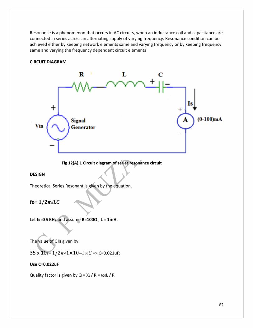
Resonance is a phenomenon that occurs in AC circuits, when an inductance coil and capacitance are connected in series across an alternating supply of varying frequency. Resonance condition can be achieved either by keeping network elements same and varying frequency or by keeping frequency same and varying the frequency dependent circuit elements CIRCUIT DIAGRAM
Fig 12(A).1 Circuit diagram of series resonance circuit
DESIGN Theoretical Series Resonant is given by the equation,
fo= 1/2𝜋√𝐿𝐶
Let f0 =35 KHz and assume R=100Ω , L = 1mH.
The value of C is given by
35 x 103= 1/2𝜋√1×10−3×𝐶 => C=0.021uF;
Use C=0.022uF
Quality factor is given by Q = XL / R = ω0L / R
63
Or
Q = XC / R = 1 / ω0CR or Q= fo / BW
Bandwidth is given by , BW = f0 / Q or BW= fo / (fH –fL)
PROCEDURE
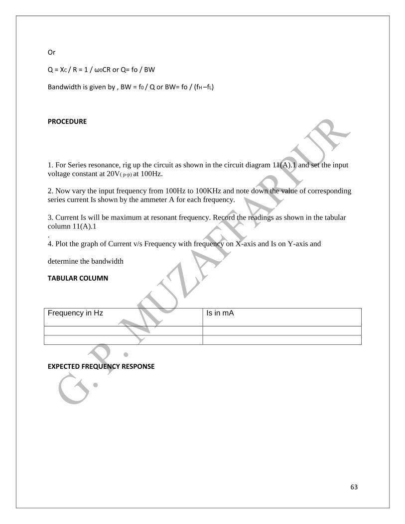
1. For Series resonance, rig up the circuit as shown in the circuit diagram 11(A).1 and set the input
voltage constant at 20V( p-p) at 100Hz.
2. Now vary the input frequency from 100Hz to 100KHz and note down the value of corresponding
series current Is shown by the ammeter A for each frequency.
3. Current Is will be maximum at resonant frequency. Record the readings as shown in the tabular
column 11(A).1
.
4. Plot the graph of Current v/s Frequency with frequency on X-axis and Is on Y-axis and
determine the bandwidth
TABULAR COLUMN
Frequency in Hz
Is in mA
EXPECTED FREQUENCY RESPONSE

64
Fig 12(A).2 Graph of Current versus Frequency
RESULT
1. Theoretical series resonant frequency f0 = ___________KHz
2. Practical series resonant frequency f0 = __________ KHz
3. Lower cut-off frequency fL= __________ KHz
4. Upper cut-off frequency fH= __________ KHz
5. Band Width BW= ( fH -fL)= __________ KHz

65
12 (B) PARALLEL RESONANCE CIRCUIT
AIM
To obtain the frequency response of an RLC parallel resonant circuit and to determine resonance
frequency.
COMPONENTS REQUIRED
THEORY
A circuit is said to be under resonance if the current flowing in the circuit is in phase with the applied
voltage that is if the whole circuit acts like a pure resistive circuit, and the circuit current will be in
phase with the voltage.
Resonance is a phenomenon and study of AC circuits, when an inductance coil and capacitance are
connected in parallel across an alternating supply of varying frequency. Resonance condition can be
achieved either by keeping network elements same and varying frequency or by keeping frequency
same and varying the frequency dependent circuit elements.
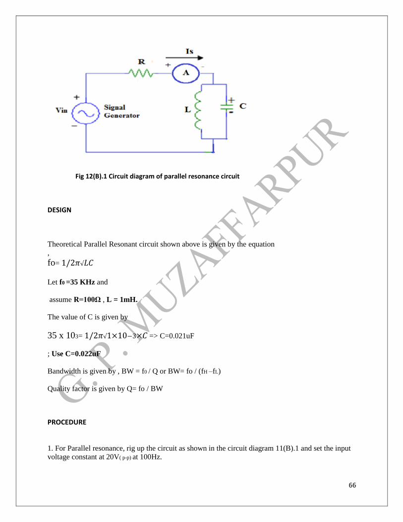
CIRCUIT DIAGRAM
66
Fig 12(B).1 Circuit diagram of parallel resonance circuit
DESIGN
Theoretical Parallel Resonant circuit shown above is given by the equation
,
fo= 1/2𝜋√𝐿𝐶 Let f0 =35 KHz and
assume R=100Ω , L = 1mH.
The value of C is given by
35 x 103= 1/2𝜋√1×10−3×𝐶 => C=0.021uF
; Use C=0.022uF
Bandwidth is given by , BW = f0 / Q or BW= fo / (fH –fL)
Quality factor is given by Q= fo / BW
PROCEDURE
1. For Parallel resonance, rig up the circuit as shown in the circuit diagram 11(B).1 and set the input voltage constant at 20V( p-p) at 100Hz.
67
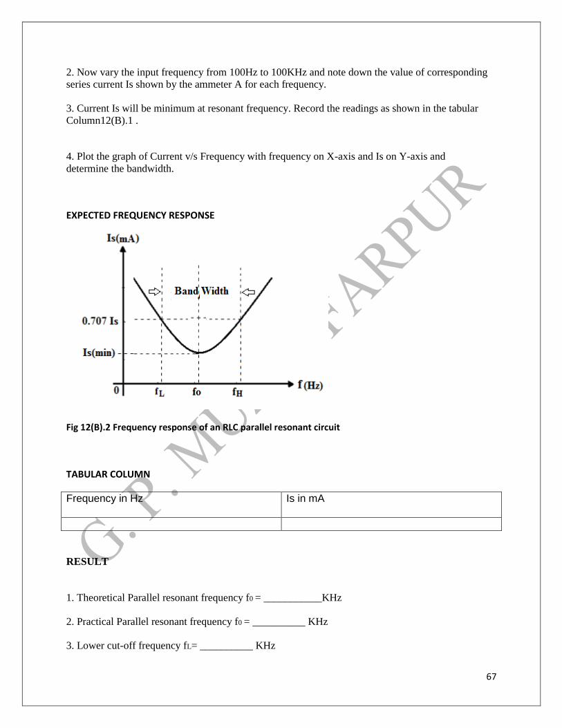
2. Now vary the input frequency from 100Hz to 100KHz and note down the value of corresponding
series current Is shown by the ammeter A for each frequency.
3. Current Is will be minimum at resonant frequency. Record the readings as shown in the tabular
Column12(B).1 .
4. Plot the graph of Current v/s Frequency with frequency on X-axis and Is on Y-axis and
determine the bandwidth.
EXPECTED FREQUENCY RESPONSE
Fig 12(B).2 Frequency response of an RLC parallel resonant circuit
TABULAR COLUMN
Frequency in Hz
Is in mA
RESULT
1. Theoretical Parallel resonant frequency f0 = ___________KHz
2. Practical Parallel resonant frequency f0 = __________ KHz
3. Lower cut-off frequency fL= __________ KHz

68
4. Upper cut-off frequency fH= __________ KHz
5. Band Width BW= ( fH -fL)= __________ KHz


![(md09-i-s82) Per star RMS Outlier histogram 1200 4•10 ... · (md09-i-s82) Per star RMS 0 10 20 30 40 50 per star sigma-clipped RMS [mmag] 0 200 400 600 800 1000 1200 number Median](https://static.fdocument.org/doc/165x107/5e0edcb7d114187d3546de0e/md09-i-s82-per-star-rms-outlier-histogram-1200-4a10-md09-i-s82-per-star.jpg)