
FLUORINE DONOR BOUND ELECTRON SPINS AS · PDF filewhich is often represented in the Bloch...
104
1 ΑΩ FLUORINE DONOR BOUND ELECTRON SPINS AS QUBITS Dem Department Physik der Universität Paderborn zur Erlangung des akademischen Grades eines Doktors der Naturwissenschaften vorgelegte Dissertation von Youngmin Martin Kim Mai 2013
-
Upload
vuongquynh -
Category
Documents
-
view
220 -
download
5
Transcript of FLUORINE DONOR BOUND ELECTRON SPINS AS · PDF filewhich is often represented in the Bloch...
1
ΑΩ
FLUORINE DONOR BOUND
ELECTRON SPINS AS QUBITS
Dem Department Physik
der Universität Paderborn
zur Erlangung des akademischen Grades
eines Doktors der Naturwissenschaften
vorgelegte
Dissertation
von
Youngmin Martin Kim
Mai 2013

2
Promotionskommission Prof. Dr. Wolf Gero Schmidt (Vorsitzender) Prof. Dr. Klaus Lischka (1. Gutachter) Prof. Dr. Thomas Zentgraf (2. Gutachter) Dr. Gerhard Berth Tag der Einreichung: 8. Mai 2013
3
Abstract
During the decades in the 1980s and 1990s, the interests on II-VI materials, e.g., ZnSe, were high for their light emitting properties in blue and green spectral range. However, experimental conclusions regarding rapid degeneration of ZnSe based LEDs and LDs under high pumping power turned the popular interests away to other material system. On the other hand, rapid developments in the quantum information science in the last few decades, called for a new device which can operate at the quantum limit, e.g., low-threshold lasers and single photon sources. Among other competing systems, semiconductor based devices provide a vantage point that the vastly cumulated knowledge and applications already existing in the field of modern electronics and photonics may be compatible with their new quantum device. Throughout this thesis, I have outlined the potentials as well as the experimental works regarding fluorine impurities in ZnSe system as a candidate for quantum information science schemes. More specifically, the bound electron spins to fluorine impurities in ZnSe QWs will be presented as qubits. In Chapter 1, some of the most fundamental definitions and required characteristics for making a quantum computer will be outlined. In Chapter 2, the basic concept of utilizing bound electron spins to fluorine impurities in ZnSe as qubits will be discussed. In Chapter 3, the material growth of ZnSe QWs and their properties will be presented. The conventional doping method of fluorine in ZnSe via molecular beam epitaxy, as well as via ion implantation as an alternative will be reported in Chapter 4. In Chapter 5, two major themes will be presented: 1) experimental processes of fabricating nanostructures for isolating individual fluorine impurities, and 2) the photoluminescence spectroscopy of the nanostructures. Finally, in Chapter 6, the presence of optically controllable qubits, as well as the ability to optically initialize and to read-out the qubit state will be demonstrated under an external magnetic field. This work helps to demonstrate the potentials of the bound electron spin states in ZnSe:F as qubits. With the ion implantation as an alternative doping method, the overall result of this thesis conveys why the fluorine impurities in ZnSe system is an attractive system for meeting the recent demands in the quantum information science.

4
5
Acknowledgement
It has been a tremendous three-year-journey of learning and development, as a PhD candidate in Paderborn. Coming from a different scientific discipline, I started in this field of experimental, solid-state based quantum information science with little preparation; thus, this work would not have been possible without many individuals who provided support and guidance.
Firstly, I would like to acknowledge Prof. Dr. Klaus Lischka who has been a wonderful supervisor to me from the beginning of my arrival in Paderborn until the end. I learned a great deal of science from his keen insight, and I always felt encouraged to go the extra mile in shaping up my thesis. As a student, I often recognized his interest as a teacher trying to compensate where I could improve further, which greatly helped me to develop.
I would like to sincerely thank PD Dr. Alexander Pawlis who was in all aspects, a vital mentor throughout my thesis. Daily, I had opportunity to learn from him by sharing the same office. His inexhaustible ideas and the ability to execute to the details of an experiment were an inspiration to me. I find it fortunate to be involved with his project, where I obtained a descent exposure to the quantum information science based on II-VI semiconductor.
I would like to thank Prof. Dr. Thomas Zentgraf for the discussion and for the encouraging support I received towards the end of the thesis. Furthermore, I want to acknowledge Prof. Dr. Wolf Gero Schmidt and Dr. Uwe Gerstmann for the intriguing discussion regarding the theoretical chapter in my thesis. I was able to connect many parts into understanding through the talks we had.
I am also thankful to my colleagues such as Marcel, Olga and Ricarda from our group, Y. Alex, Dirk and Wadim in AG Zrenner, and Holger in AG Zentgraf for the practical idea and help in and out of the laboratory.
I am greatly indebted to my parents who provided love and care, to whom I owe my source of resilient strength in difficult times. Above all, I bow to God who orchestrated all things to come to pass pruning my character throughout this experience, having been my present help in time of need.

6
חכמה תחלת יראת יהוה ודעת קדשים בינה׃
“The fear of the LORD is the beginning of wisdom: and the knowledge of the holy is understanding.”
Proverbs of Solomon 9:10
7
Contents
Abstract
Acknowledgements
1. Introduction 9 1.1. Definitions and Criteria……………………………...….…… 10 1.2. Comparison of few selected physical system ………....……... 12
2. Bound electron spins of fluorine impurities in ZnSe 15 2.1. Effective mass approximation …………….………………..... 16 2.2. Fluorine donor states in ZnSe ……………….……………… 16
2.2.1. Incorporation of fluorine in ZnSe as a donor and the relevant optical transitions
3. Material growth of ZnMgSe/ZnSe QWs 19 3.1. Growth of ZnMgSe/ZnSe QWs ……………………...…….. 19 3.2. Properties of ZnMgSe/ZnSe QWs ………..………….…….. 22
3.2.1. Band diagram of ZnMgSe/ZnSe QW ……..………….…… 22
3.2.2. Quantum-well confinement energy …………...…….……... 23
3.2.3. Exciton binding energy in the QW-confinement ……...……. 25
3.3. Summary ………………………………………….…..……... 26
4. Fluorine Doping of ZnSe 27 4.1. Fluorine doping of ZnSe in MBE ……..……………...…….... 27
4.1.1. Fluorine δ-doping in ZnSe QWs ……….…………..……... 27
4.1.2. Electrical characterization of fluorine donors in ZnSe …...….. 30
4.1.3. Optical characterization of fluorine donors in ZnSe …..….…. 33
4.1.4. Limitation of MBE fluorine doping ……….…………….… 34
4.2. Fluorine doping of ZnSe in MBE with a cracker cell ……..... 35 4.2.1. Thermal dissociation of ZnF2 by a cracker cell.……….….…. 35
4.2.2. Fluorine doping via migration enhanced epitaxy (MEE).….… 38
4.2.3. Rapid thermal annealing …………..……………………... 41
8
4.3. Fluorine Ion Implantation ………………………………...… 43 4.3.1. Mechanism of ion implantation.……………....…………… 44
4.3.2. Selective ion implantation …………………..……………. 46
4.4. Summary.……………………………………..……………… 49
5. Isolation of individual impurities and Photoluminescence spectroscopy 51 5.1. Fabrication of ZnMgSe/ZnSe nanoposts ….…………..…… 52
5.1.1. Electron beam lithography ….....………………..………... 53
5.1.2. Proximity effect on ZnSe ………………………..……….. 53
5.1.3. The etching of ZnSe ………….…………………..……… 56
5.1.4. SeO2 surface clustering on ZnSe …………………..……… 57
5.2. Photoluminescence spectroscopy of individual impurities in nanostructures …………..……....……………………….... 61 5.2.1. The μ-photoluminescence spectroscopy setup ………...…….. 61 5.2.2. Photoluminescence spectroscopy of F- implanted
ZnSe QWs nanostructures …………..…………………… 63
5.3. Summary ……………...….……..……………………………. 68
6. Bound electron spins under external magnetic field 69 6.1. Non-degenerate donor states under Zeeman splitting ….….. 69
6.1.1. g-factors of electrons and holes in ZnSe QWs ……..……….. 71
6.2. Magneto spectroscopy in Faraday and Voigt geometry......… 72 6.2.1. Magneto-optics setup……………………..……………… 72 6.2.2. Optical transitions by selection rules………..……………… 81
6.2.3. Optical characterizations…………………….…………… 82
6.3. Optical pumping and initialization of qubits …….………….. 85 6.3.1. Measurement system ….…………....……………………. 85
6.3.2. Optical pumping experiment …………....………………… 86
6.4. Summary ………………………………..…………………….. 90
7. Conclusion and Outlook 91
Appendix A. Derivation of Bloch sphere representation of qubits……..….. 93 B. Summary of ZnSe technology recipes…….………………… 95
Bibliography 97
9
Chapter 1
Introduction Over the last few decades, quantum information science has gone through tremendous experimental progresses. Perhaps one of the greatest landmarks regards to the development of a quantum computer. In 1975, R. P. Poplavskii published "Thermo-dynamical models of information processing" [1] which showed the computational impossibility of simulating quantum systems on classical computers, due to the superposition principle. In 1981, Richard P. Feynman, in his famous talk at the First Conference on the Physics of Computation at MIT, observed that it appeared to be infeasible to simulate the propagation of a quantum system on a classical computer with sufficient accuracy. He suggested a ground model for a quantum computer that would enable such simulations [2]. Since then, the idea of building a computing system governed by the laws of quantum mechanics has led a number of physical systems to emerge to realize a new kind of computational power utilizing much of the forefront concepts and applications from the quantum theory of physics. The calculation potential of a quantum computer is much expected to be superior to a classical computer in certain tasks. For an instance, in Shor’s algorithm of factoring large numbers, a modest sized quantum computer is expected to outperform the most powerful classical supercomputers [3]. It could also simulate scientific models considered challenging for classical computers such as quantum phase transition, high-temperature superconductivity, lattice gauge theories, Hawking radiation in black holes, the rate of expansion of the universe, and sharing secured information guaranteed by the laws of quantum mechanics. [4] For reviewing more detailed overview of different quantum computing systems, the readers are recommended to review Ref. [5, 6].
Before further delving into the course, I would like to outline some fundamental terms which may be repeatedly referred in the subsequent chapters. Furthermore, there are several requirements considered fundamental that a robust quantum computer must demonstrate which will also be described in this chapter.
10
1.1. Definitions and Criteria
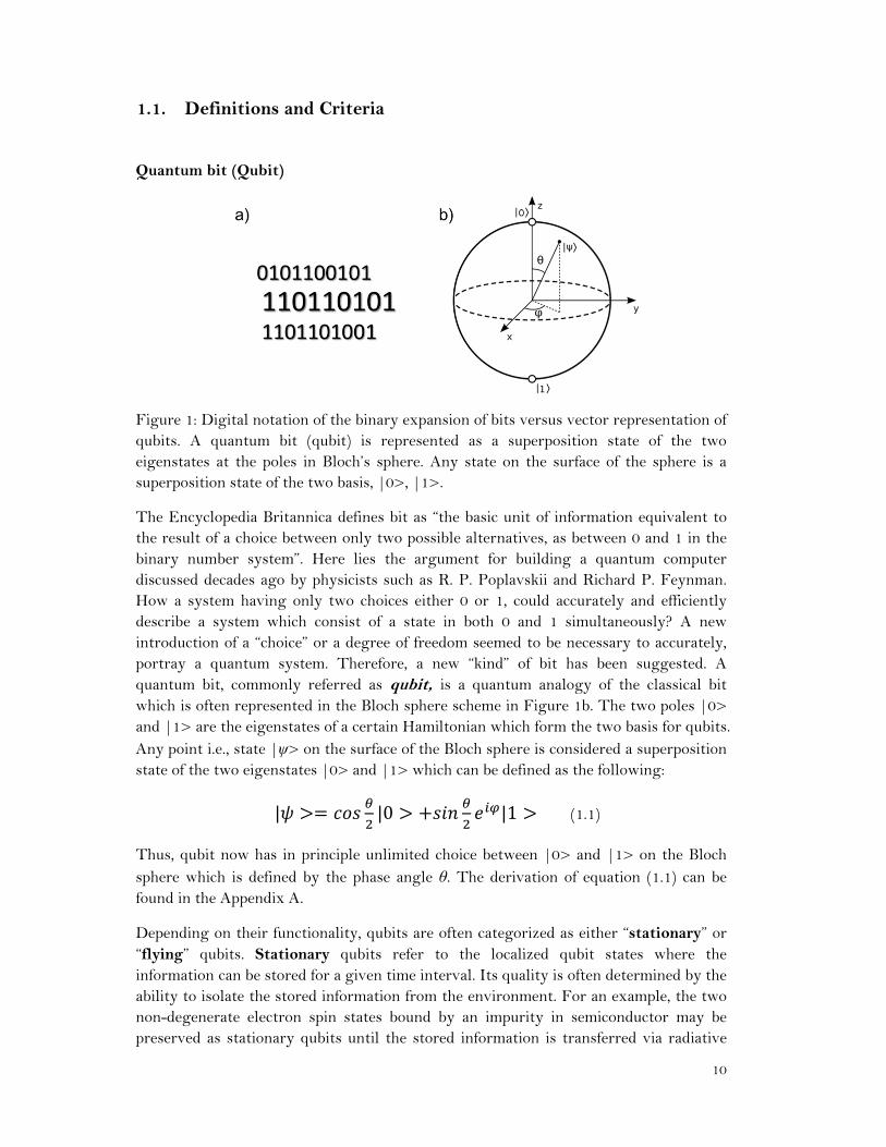
Quantum bit (Qubit)
Figure 1: Digital notation of the binary expansion of bits versus vector representation of qubits. A quantum bit (qubit) is represented as a superposition state of the two eigenstates at the poles in Bloch’s sphere. Any state on the surface of the sphere is a superposition state of the two basis, |0>, |1>.
The Encyclopedia Britannica defines bit as “the basic unit of information equivalent to the result of a choice between only two possible alternatives, as between 0 and 1 in the binary number system”. Here lies the argument for building a quantum computer discussed decades ago by physicists such as R. P. Poplavskii and Richard P. Feynman. How a system having only two choices either 0 or 1, could accurately and efficiently describe a system which consist of a state in both 0 and 1 simultaneously? A new introduction of a “choice” or a degree of freedom seemed to be necessary to accurately, portray a quantum system. Therefore, a new “kind” of bit has been suggested. A quantum bit, commonly referred as qubit, is a quantum analogy of the classical bit which is often represented in the Bloch sphere scheme in Figure 1b. The two poles |0> and |1> are the eigenstates of a certain Hamiltonian which form the two basis for qubits. Any point i.e., state |ψ> on the surface of the Bloch sphere is considered a superposition state of the two eigenstates |0> and |1> which can be defined as the following:
| |0 |1 (1.1)
Thus, qubit now has in principle unlimited choice between |0> and |1> on the Bloch sphere which is defined by the phase angle θ. The derivation of equation (1.1) can be found in the Appendix A.
Depending on their functionality, qubits are often categorized as either “stationary” or “flying” qubits. Stationary qubits refer to the localized qubit states where the information can be stored for a given time interval. Its quality is often determined by the ability to isolate the stored information from the environment. For an example, the two non-degenerate electron spin states bound by an impurity in semiconductor may be preserved as stationary qubits until the stored information is transferred via radiative
11
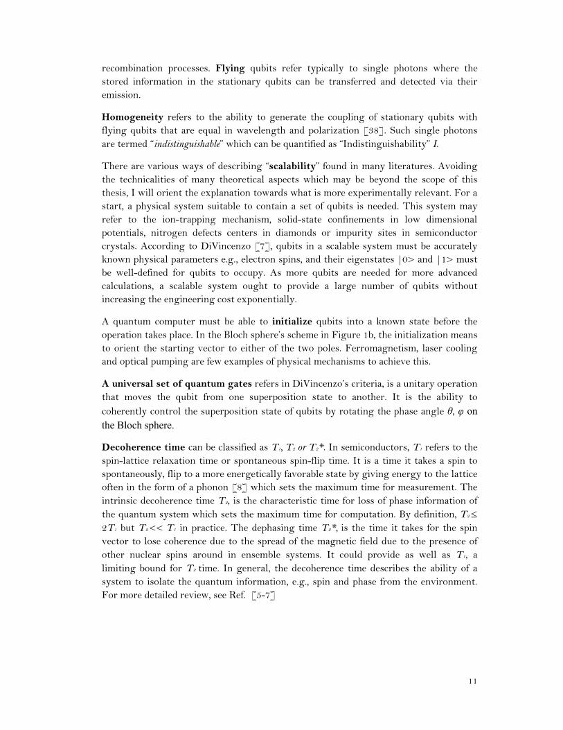
recombination processes. Flying qubits refer typically to single photons where the stored information in the stationary qubits can be transferred and detected via their emission.
Homogeneity refers to the ability to generate the coupling of stationary qubits with flying qubits that are equal in wavelength and polarization [38]. Such single photons are termed “indistinguishable” which can be quantified as “Indistinguishability” I.
There are various ways of describing “scalability” found in many literatures. Avoiding the technicalities of many theoretical aspects which may be beyond the scope of this thesis, I will orient the explanation towards what is more experimentally relevant. For a start, a physical system suitable to contain a set of qubits is needed. This system may refer to the ion-trapping mechanism, solid-state confinements in low dimensional potentials, nitrogen defects centers in diamonds or impurity sites in semiconductor crystals. According to DiVincenzo [7], qubits in a scalable system must be accurately known physical parameters e.g., electron spins, and their eigenstates |0> and |1> must be well-defined for qubits to occupy. As more qubits are needed for more advanced calculations, a scalable system ought to provide a large number of qubits without increasing the engineering cost exponentially.
A quantum computer must be able to initialize qubits into a known state before the operation takes place. In the Bloch sphere’s scheme in Figure 1b, the initialization means to orient the starting vector to either of the two poles. Ferromagnetism, laser cooling and optical pumping are few examples of physical mechanisms to achieve this.
A universal set of quantum gates refers in DiVincenzo’s criteria, is a unitary operation that moves the qubit from one superposition state to another. It is the ability to coherently control the superposition state of qubits by rotating the phase angle θ, φ on the Bloch sphere.
Decoherence time can be classified as T1, T2 or T2*. In semiconductors, T1 refers to the spin-lattice relaxation time or spontaneous spin-flip time. It is a time it takes a spin to spontaneously, flip to a more energetically favorable state by giving energy to the lattice often in the form of a phonon [8] which sets the maximum time for measurement. The intrinsic decoherence time T2, is the characteristic time for loss of phase information of the quantum system which sets the maximum time for computation. By definition, T2 ≤
2T1 but T2 << T1 in practice. The dephasing time T2*, is the time it takes for the spin vector to lose coherence due to the spread of the magnetic field due to the presence of other nuclear spins around in ensemble systems. It could provide as well as T1, a limiting bound for T2 time. In general, the decoherence time describes the ability of a system to isolate the quantum information, e.g., spin and phase from the environment. For more detailed review, see Ref. [5-7]
12
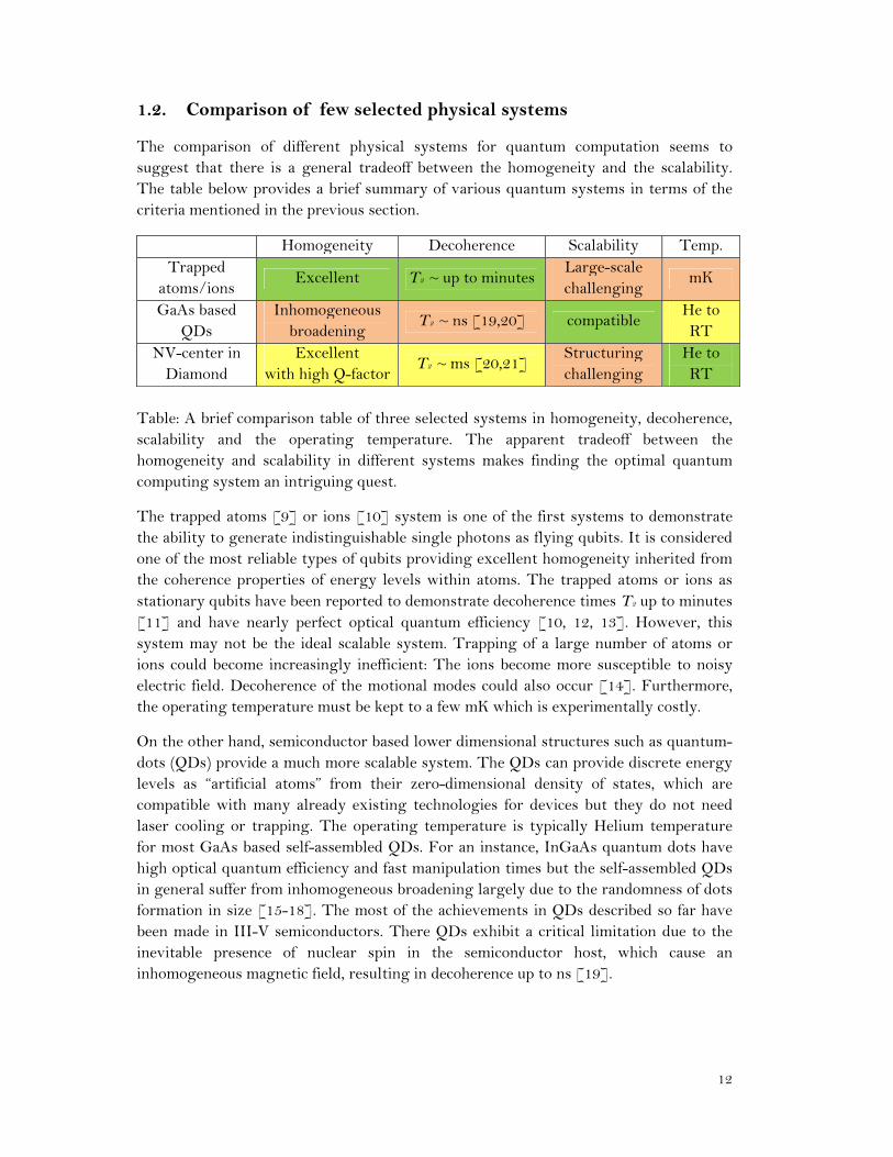
1.2. Comparison of few selected physical systems
The comparison of different physical systems for quantum computation seems to suggest that there is a general tradeoff between the homogeneity and the scalability. The table below provides a brief summary of various quantum systems in terms of the criteria mentioned in the previous section.
Homogeneity Decoherence Scalability Temp. Trapped
atoms/ions Excellent T2 ~ up to minutes
Large-scale challenging
mK
GaAs based QDs
Inhomogeneous broadening
T2 ~ ns [19,20] compatible He to RT
NV-center in Diamond
Excellent with high Q-factor
T2 ~ ms [20,21] Structuring challenging
He to RT
Table: A brief comparison table of three selected systems in homogeneity, decoherence, scalability and the operating temperature. The apparent tradeoff between the homogeneity and scalability in different systems makes finding the optimal quantum computing system an intriguing quest.
The trapped atoms [9] or ions [10] system is one of the first systems to demonstrate the ability to generate indistinguishable single photons as flying qubits. It is considered one of the most reliable types of qubits providing excellent homogeneity inherited from the coherence properties of energy levels within atoms. The trapped atoms or ions as stationary qubits have been reported to demonstrate decoherence times T2 up to minutes [11] and have nearly perfect optical quantum efficiency [10, 12, 13]. However, this system may not be the ideal scalable system. Trapping of a large number of atoms or ions could become increasingly inefficient: The ions become more susceptible to noisy electric field. Decoherence of the motional modes could also occur [14]. Furthermore, the operating temperature must be kept to a few mK which is experimentally costly.
On the other hand, semiconductor based lower dimensional structures such as quantum-dots (QDs) provide a much more scalable system. The QDs can provide discrete energy levels as “artificial atoms” from their zero-dimensional density of states, which are compatible with many already existing technologies for devices but they do not need laser cooling or trapping. The operating temperature is typically Helium temperature for most GaAs based self-assembled QDs. For an instance, InGaAs quantum dots have high optical quantum efficiency and fast manipulation times but the self-assembled QDs in general suffer from inhomogeneous broadening largely due to the randomness of dots formation in size [15-18]. The most of the achievements in QDs described so far have been made in III-V semiconductors. There QDs exhibit a critical limitation due to the inevitable presence of nuclear spin in the semiconductor host, which cause an inhomogeneous magnetic field, resulting in decoherence up to ns [19].
13
Nitrogen vacancy centers in diamond have a longer decoherence time than QDs up to few ms because of the nearly spin free Carbon lattice and low spin-orbit coupling which remain relatively long in room temperature [20, 21]. From isotopically enriched 12C diamond, T2 has been reported to be 2 ms for 99.7% pure material [22]. However, the zero-phonon line used for coupling in NV centers is optically weaker than the transitions provided by QDs. Thus, high-Q micro-cavities to compensate the quantum efficiency are essential, but the fabrication of such cavities with diamond is non-trivial.
Another intriguing semiconductor based qubit system is ZnSe (group II-VI) with fluorine donors, which is the investigated system of this thesis. The electron spins bound to fluorine impurities in ZnSe have several advantages, which may bridge the gap between the trapped atoms for their excellent homogeneity and the artificial atoms (QDs) for their scalability. Here I outline some of its properties:
The ZnSe has a direct bandgap of 2.8 eV which provides high optical quantum efficiency of the relevant transitions in the three-level lambda system. The fluorine impurities form donor-like states [24, 25] with the ionization energy of about 29 meV [26], which provides substantial thermal stability for qubits [27]. While the hyperfine interaction between the electron spin and the nuclear spin of the host material is the principal cause for decoherence in III-V based QDs [28], the ZnSe host material can be isotopically purified to deplete the nuclear spins, which may prolong the decoherence time beyond that of III-V based QDs. Moreover, the 100% natural abundance of the spin-1/2 in 19F nucleus may further increase the decoherence time by transferring the information stored in electron to the nuclear spin. From the radiative recombination lifetime of a bound exciton; 100 ps [29], the homogeneous linewidth for a single emitter limited by the lifetime can be inferred; 1-2 GHz. Furthermore, it has been shown that the photons from two independent QW-nanostructures provide sufficient indistinguishability [29] to generate photon-photon entanglement through postselection [30]. Recently, it has been reported that an ensemble of fluorine donors in ZnSe features an electron spin dephasing time T2* greater than 30 ns up to 40K [27]. In this thesis, I will demonstrate the overall experimental processes of establishing such qubit system. The ion implantation of fluorine into ZnSe as active donors in Chapter 4, which has been successfully demonstrated [31], could lead to deterministically introducing single donors in specific locations. The possibility of post-registration of fluorine impurities as active donors into undoped ZnSe micro-, nano-cavities may provide a basis for the architecture of quantum repeaters. The magneto-spectroscopy of our optical system in Chapter 6 demonstrates the fully-connected nature of our optical lambda system. All of these characteristics make fluorine impurities in ZnSe system an appealing qubit candidate for quantum information technology.

14
In conclusion, there is an apparent tradeoff between the homogeneity and the scalability among various competing systems which makes finding the ideal quantum computing system an intriguing quest. The decoherence time T2 must be considered together with the read-out rate. The ratio between these two parameters thus gives the operational capacity which for most state-of-the-art devices shows in the order of 103-104. Moreover, taking account the ability to generate pure entangled states over micro-, and macroscopic distances in different systems further complicates the matter to decide the winner for this quest. Further research in the next few decades may finally determine the answer to the question: What form does a quantum computer have?
15
Chapter 2
Bound electron spins by fluorine impurities in ZnSe
In the previous section 1.2, the potential of fluorine impurities in ZnSe system were described. In this chapter, the fluorine donor states in ZnSe and the relevant optical transitions suitable for quantum computing will be further expounded.
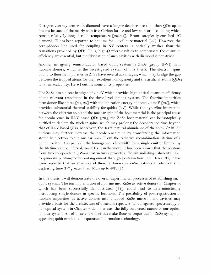
Semiconductor electron spins confined by an impurity potential naturally form a specific quantum system. The degeneracy of the spin states at Γ -point, as in many semiconductors, can be lifted via Zeeman splitting under an external magnetic field defining a two-state basis for stationary qubits [8]. The optical transitions from this two-state basis connected with an excited state form a three-level lambda system.
Figure 2: three-level lambda system. The two ground states are connected with an excited state to form a three level system where an electron may change its quantum state through an excited state.
Figure 2 portrays a three-level lambda system where the quantum information, e.g., the spin states can be stored and manipulated for quantum computation. The energy splitting of the two ground states can be tens of gigahertz in ZnSe:F system [31-32] which can be manipulated directly with microwaves [23], oscillating electric fields [33], or by the exchange interaction between nearby electron spins with gate voltages [34-35].
16
2.1. Effective mass approximation
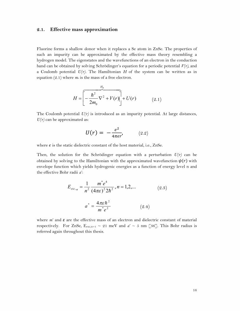
Fluorine forms a shallow donor when it replaces a Se atom in ZnSe. The properties of such an impurity can be approximated by the effective mass theory resembling a hydrogen model. The eigenstates and the wavefunctions of an electron in the conduction band can be obtained by solving Schrödinger’s equation for a periodic potential V(r), and a Coulomb potential U(r). The Hamiltonian H of the system can be written as in equation (2.1) where m0 is the mass of a free electron.
)()(2
0
2
0
2
rUrVm
H
H
(2.1)
The Coulomb potential U(r) is introduced as an impurity potential. At large distances, U(r) can be approximated as:
, (2.2)
where is the static dielectric constant of the host material, i.e., ZnSe.
Then, the solution for the Schrödinger equation with a perturbation U(r) can be
obtained by solving to the Hamiltonian with the approximated wavefunction with envelope function which yields hydrogenic energies as a function of energy level n and the effective Bohr radii a*:
,...2,1,2)4(
122
4*
2, nem
nE
nexc (2.3)
2*
2* 4
ema
(2.4)
where m* and ɛ are the effective mass of an electron and dielectric constant of material respectively. For ZnSe, Eexc,n=1 ~ 21 meV and a* ~ 5 nm [36]. This Bohr radius is referred again throughout this thesis.
17
2.2. Fluorine donor states in ZnSe
2.2.1. Incorporation of fluorine in ZnSe as a donor and the relevant optical transitions
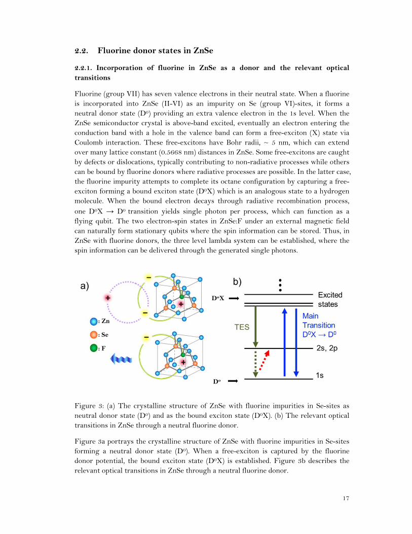
Fluorine (group VII) has seven valence electrons in their neutral state. When a fluorine is incorporated into ZnSe (II-VI) as an impurity on Se (group VI)-sites, it forms a neutral donor state (D0) providing an extra valence electron in the 1s level. When the ZnSe semiconductor crystal is above-band excited, eventually an electron entering the conduction band with a hole in the valence band can form a free-exciton (X) state via Coulomb interaction. These free-excitons have Bohr radii, ~ 5 nm, which can extend over many lattice constant (0.5668 nm) distances in ZnSe. Some free-excitons are caught by defects or dislocations, typically contributing to non-radiative processes while others can be bound by fluorine donors where radiative processes are possible. In the latter case, the fluorine impurity attempts to complete its octane configuration by capturing a free-exciton forming a bound exciton state (D0X) which is an analogous state to a hydrogen molecule. When the bound electron decays through radiative recombination process, one D0X → D0 transition yields single photon per process, which can function as a flying qubit. The two electron-spin states in ZnSe:F under an external magnetic field can naturally form stationary qubits where the spin information can be stored. Thus, in ZnSe with fluorine donors, the three level lambda system can be established, where the spin information can be delivered through the generated single photons.
Figure 3: (a) The crystalline structure of ZnSe with fluorine impurities in Se-sites as neutral donor state (D0) and as the bound exciton state (D0X). (b) The relevant optical transitions in ZnSe through a neutral fluorine donor.
Figure 3a portrays the crystalline structure of ZnSe with fluorine impurities in Se-sites forming a neutral donor state (D0). When a free-exciton is captured by the fluorine donor potential, the bound exciton state (D0X) is established. Figure 3b describes the relevant optical transitions in ZnSe through a neutral fluorine donor.
18
The main transition refers to the radiative recombination of a bound exciton in D0X state to D0 emitting a single photon. The emission energy (in bulk) corresponds to:
DXXZnSegph EEEE )( (2.5)
Where Eph, Eg, EX, EDX represents the emission energy, material bandgap, binding energy of a free-exciton, and the binding energy of a bound exciton respectively. The two-electron satellite transition (TES) occurs when a portion of the emitted photon’s energy in the main transition is absorbed by the other remaining electron at the donor exciting the second electron to the 2s or the 2p state. A typical energy separation of TES line from the DoX is about 20 – 22 meV. The binding energy of an exciton in ZnSe can be approximated by Hayne’s rule [37]:
≡∗
∗ (2.6)
where , are the exciton binding energy and the donor ionization energy
respectively. The function∗
∗ is a fitting function of the ratio between the effective
mass of an electron and a hole in the crystal. For typical II-VI compounds, me*/mh* 0.25 and the experimental results suggest (0.25) 0.2 [37], thus considering the fluorine donor ionization energy in ZnSe to be about 29 meV, the exciton binding energy in bulk ZnSe can be approximated to be about 6 meV.
19
Chapter 3
Material growth of ZnMgSe/ZnSe Quantum- wells (QWs)
All samples investigated in this thesis are molecular beam epitaxy (MBE) grown hetero-structures containing quantum-well (QW) confinements. There are several motivations of introducing QW confinements into ZnSe:F system. The Zn1-xMgxSe layers, containing 5 – 15% Mg concentration function as barriers or cladding layers enhancing the optical brightness. With these barriers, the electrons and holes are more probable to fall into ZnSe QW active region instead of leaking into GaAs or to the surface. Also, the inhomogeneous broadening can be made less by reducing the volume of the active zone. Furthermore, an increasing binding energy of exciton can be expected because of the compression of the donor wavefunction in the QWs.
3.1. Growth of ZnMgSe/ZnSe QWs
The ZnSe is grown on commercially available GaAs substrates by Molecular Beam Epitaxy (MBE). A small lattice mismatch of 0.2 – 0.3 % between the GaAs and ZnSe provides a favorable crystallization condition for two-dimensional growth [38]. Nevertheless, this lattice mismatch introduces a compressive strain of ZnSe layer on GaAs which lifts up the degeneracy of the heavy-hole (hh) and light-hole (lh) states.
20
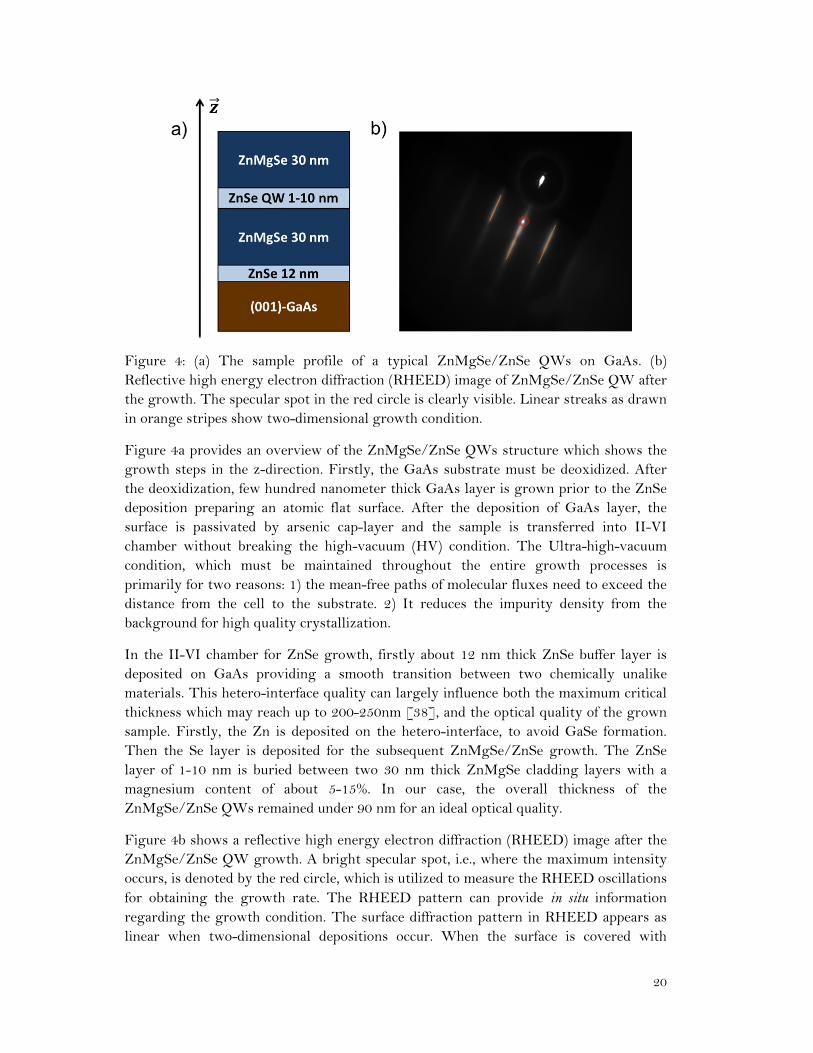
Figure 4: (a) The sample profile of a typical ZnMgSe/ZnSe QWs on GaAs. (b) Reflective high energy electron diffraction (RHEED) image of ZnMgSe/ZnSe QW after the growth. The specular spot in the red circle is clearly visible. Linear streaks as drawn in orange stripes show two-dimensional growth condition.
Figure 4a provides an overview of the ZnMgSe/ZnSe QWs structure which shows the growth steps in the z-direction. Firstly, the GaAs substrate must be deoxidized. After the deoxidization, few hundred nanometer thick GaAs layer is grown prior to the ZnSe deposition preparing an atomic flat surface. After the deposition of GaAs layer, the surface is passivated by arsenic cap-layer and the sample is transferred into II-VI chamber without breaking the high-vacuum (HV) condition. The Ultra-high-vacuum condition, which must be maintained throughout the entire growth processes is primarily for two reasons: 1) the mean-free paths of molecular fluxes need to exceed the distance from the cell to the substrate. 2) It reduces the impurity density from the background for high quality crystallization.
In the II-VI chamber for ZnSe growth, firstly about 12 nm thick ZnSe buffer layer is deposited on GaAs providing a smooth transition between two chemically unalike materials. This hetero-interface quality can largely influence both the maximum critical thickness which may reach up to 200-250nm [38], and the optical quality of the grown sample. Firstly, the Zn is deposited on the hetero-interface, to avoid GaSe formation. Then the Se layer is deposited for the subsequent ZnMgSe/ZnSe growth. The ZnSe layer of 1-10 nm is buried between two 30 nm thick ZnMgSe cladding layers with a magnesium content of about 5-15%. In our case, the overall thickness of the ZnMgSe/ZnSe QWs remained under 90 nm for an ideal optical quality.
Figure 4b shows a reflective high energy electron diffraction (RHEED) image after the ZnMgSe/ZnSe QW growth. A bright specular spot, i.e., where the maximum intensity occurs, is denoted by the red circle, which is utilized to measure the RHEED oscillations for obtaining the growth rate. The RHEED pattern can provide in situ information regarding the growth condition. The surface diffraction pattern in RHEED appears as linear when two-dimensional depositions occur. When the surface is covered with
21
pseudo two-dimensional or three-dimensional formations, the randomly scattered electrons form volumic diffraction patterns broadening eventually like circular shapes. The linear streaks marked with orange stripes in Figure 4b show two-dimensional growth quality of ZnMgSe/ZnSe on GaAs.
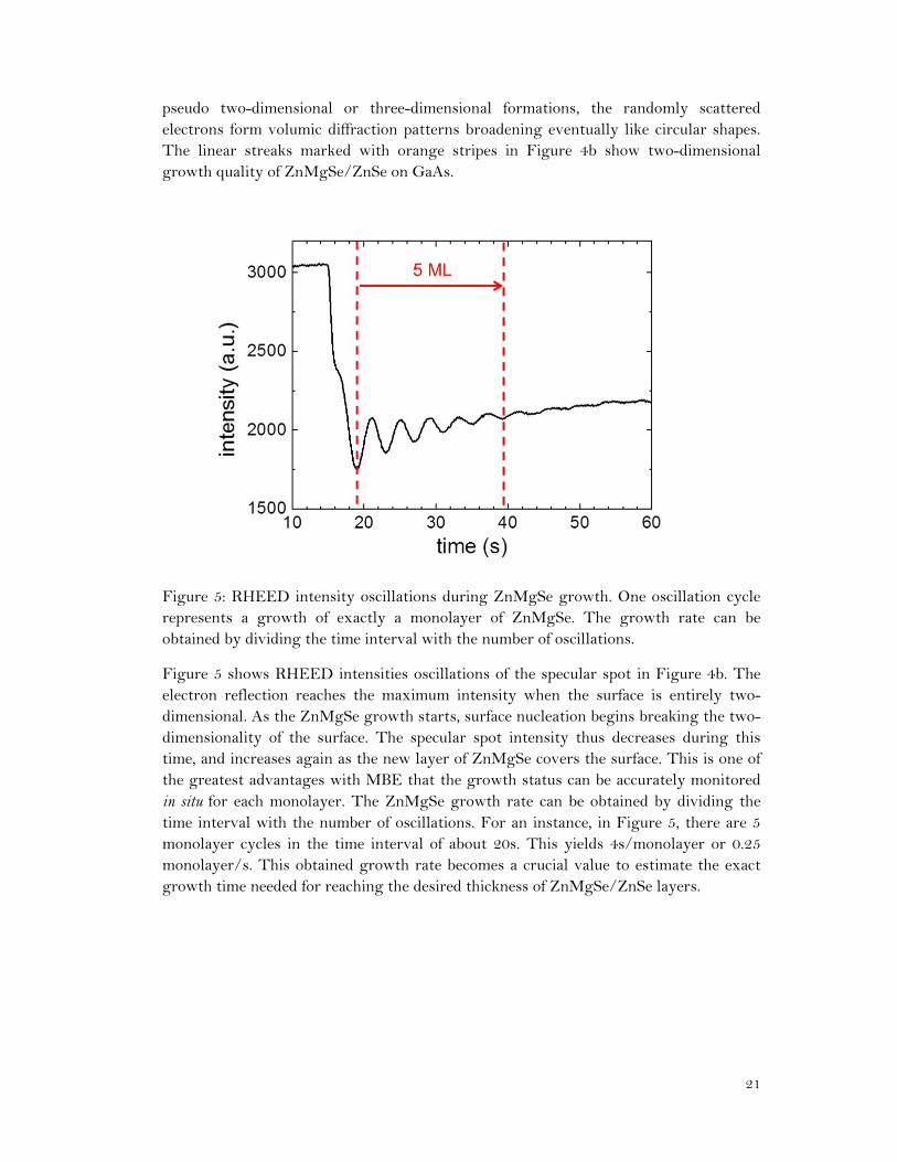
Figure 5: RHEED intensity oscillations during ZnMgSe growth. One oscillation cycle represents a growth of exactly a monolayer of ZnMgSe. The growth rate can be obtained by dividing the time interval with the number of oscillations.
Figure 5 shows RHEED intensities oscillations of the specular spot in Figure 4b. The electron reflection reaches the maximum intensity when the surface is entirely two-dimensional. As the ZnMgSe growth starts, surface nucleation begins breaking the two-dimensionality of the surface. The specular spot intensity thus decreases during this time, and increases again as the new layer of ZnMgSe covers the surface. This is one of the greatest advantages with MBE that the growth status can be accurately monitored in situ for each monolayer. The ZnMgSe growth rate can be obtained by dividing the time interval with the number of oscillations. For an instance, in Figure 5, there are 5 monolayer cycles in the time interval of about 20s. This yields 4s/monolayer or 0.25 monolayer/s. This obtained growth rate becomes a crucial value to estimate the exact growth time needed for reaching the desired thickness of ZnMgSe/ZnSe layers.
22
3.2. Properties of ZnMgSe/ZnSe QWs
3.2.1. Band diagram of ZnMgSe/ZnSe QW
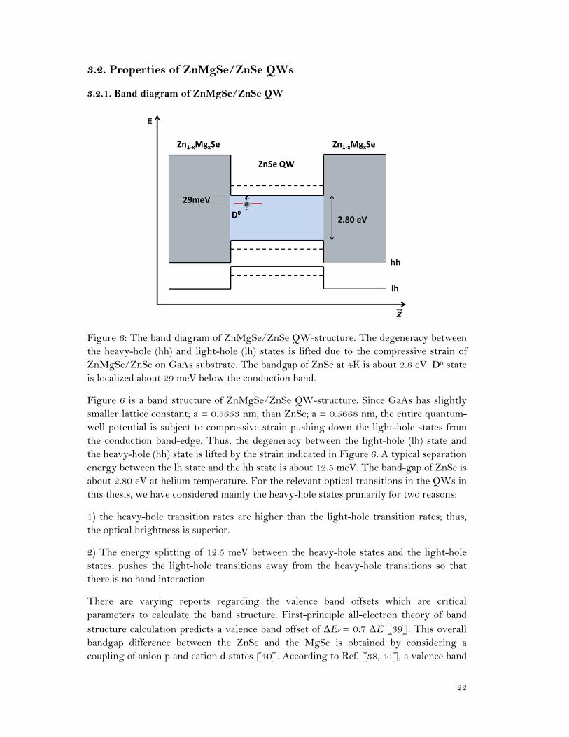
Figure 6: The band diagram of ZnMgSe/ZnSe QW-structure. The degeneracy between the heavy-hole (hh) and light-hole (lh) states is lifted due to the compressive strain of ZnMgSe/ZnSe on GaAs substrate. The bandgap of ZnSe at 4K is about 2.8 eV. D0 state is localized about 29 meV below the conduction band.
Figure 6 is a band structure of ZnMgSe/ZnSe QW-structure. Since GaAs has slightly smaller lattice constant; a = 0.5653 nm, than ZnSe; a = 0.5668 nm, the entire quantum-well potential is subject to compressive strain pushing down the light-hole states from the conduction band-edge. Thus, the degeneracy between the light-hole (lh) state and the heavy-hole (hh) state is lifted by the strain indicated in Figure 6. A typical separation energy between the lh state and the hh state is about 12.5 meV. The band-gap of ZnSe is about 2.80 eV at helium temperature. For the relevant optical transitions in the QWs in this thesis, we have considered mainly the heavy-hole states primarily for two reasons:
1) the heavy-hole transition rates are higher than the light-hole transition rates; thus, the optical brightness is superior.
2) The energy splitting of 12.5 meV between the heavy-hole states and the light-hole states, pushes the light-hole transitions away from the heavy-hole transitions so that there is no band interaction.
There are varying reports regarding the valence band offsets which are critical parameters to calculate the band structure. First-principle all-electron theory of band structure calculation predicts a valence band offset of ΔEV = 0.7 ΔE [39]. This overall bandgap difference between the ZnSe and the MgSe is obtained by considering a coupling of anion p and cation d states [40]. According to Ref. [38, 41], a valence band
23
offset of ΔEV = 0.87 ΔE was deduced from the photoluminescence (PL) and the photoelectron spectroscopy of ZnMgSe/ZnSe QWs with Mg content less than 30 %.
3.2.2. Quantum-well confinement energy
The quantization of the motion of the electrons and holes in one direction provides an increased energy at rest by the quantum confinement energy:
Tkzmm
pE B
ztconfinemen 2
1
)(2~
2
)(2
22
(3.1)
∆z (3.2)
This confinement energy becomes significant only if it is comparable to or greater than the kinetic energy of the electron due to its thermal motion in the z-direction [42] according to equation (3.2). With me* = 0.21m0, Δz 3.7 nm at room temperature for ZnSe, in order to clearly, demonstrate quantum effects, the thicknesses of the ZnSe QWs are often realized between 1 nm - 10 nm.
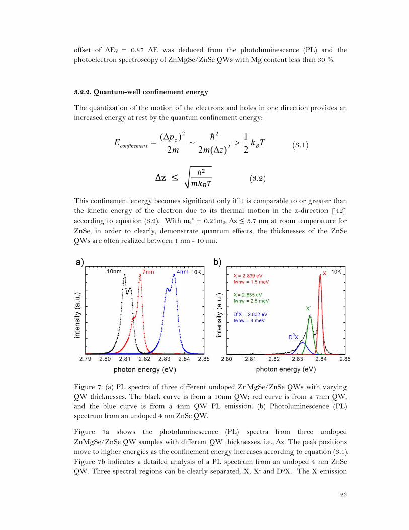
Figure 7: (a) PL spectra of three different undoped ZnMgSe/ZnSe QWs with varying QW thicknesses. The black curve is from a 10nm QW; red curve is from a 7nm QW, and the blue curve is from a 4nm QW PL emission. (b) Photoluminescence (PL) spectrum from an undoped 4 nm ZnSe QW.
Figure 7a shows the photoluminescence (PL) spectra from three undoped ZnMgSe/ZnSe QW samples with different QW thicknesses, i.e., Δz. The peak positions move to higher energies as the confinement energy increases according to equation (3.1). Figure 7b indicates a detailed analysis of a PL spectrum from an undoped 4 nm ZnSe QW. Three spectral regions can be clearly separated; X, X- and D0X. The X emission
24
peak is the radiative recombination of the heavy-hole free-excitons. The X- peak corresponds to the trion state or the charged free-exciton complex, which is often observed in II-VI semiconductors [43, 27]. This transition is generated when a free-exciton is charged by an electron in the QWs. The D0X peak refers to the bound exciton emission which is due to the radiative recombination processes of excitons bound to neutral donors.
Although this QW sample in Figure 7b is not intentionally doped, the presence of D0X shows the embedded background impurity level as donors in the MBE chamber. The optical linewidth of X is 1.5 meV, which can be further reduced to around 1.0 meV for the 10 nm QWs under optimized growth conditions.
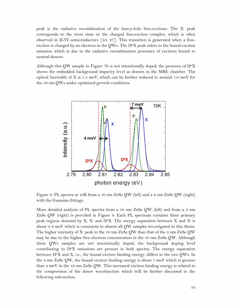
Figure 8: PL spectra at 10K from a 10 nm ZnSe QW (left) and a 4 nm ZnSe QW (right) with the Gaussian fittings.
More detailed analysis of PL spectra from a 10 nm ZnSe QW (left) and from a 4 nm ZnSe QW (right) is provided in Figure 8. Each PL spectrum contains three primary peak regions denoted by X, X- and D0X. The energy separation between X and X- is about 3-4 meV which is consistent in almost all QW samples investigated in this thesis. The higher intensity of X- peak in the 10 nm ZnSe QW than that of the 4 nm ZnSe QW may be due to the higher free electron concentration in the 10 nm ZnSe QW. Although these QWs samples are not intentionally doped, the background doping level contributing to D0X emissions are present in both spectra. The energy separation between D0X and X, i.e., the bound exciton binding energy, differs in the two QWs. In the 4 nm ZnSe QW, the bound exciton binding energy is about 7 meV which is greater than 4 meV in the 10 nm ZnSe QW. This increased exciton binding energy is related to the compression of the donor wavefunction which will be further discussed in the following sub-section.
25
3.2.3. Exciton binding energy in the QW-confinement
The binding energy of an exciton to a fluorine impurity has been suggested by Haynes’ rule to be about 5-6 meV in ZnSe [37] without considering additional QW-confinement, which is a good approximation for many 10 nm ZnSe QW samples we examined.
However, it is likely that the QW-confinement does influence the exciton binding energy as the confinement length becomes comparable to twice the Bohr radius of exciton. To gain an estimation of the QW-effect on the exciton binding energy, variational method for hydrogenic states in the QW-confinement can be used [44-45] which has been applied for ZnMgSe/ZnSe QW-confinement in Ref. [8]. This result shows a thickness dependence on the binding energy with a maximum occurring around 3 nm ZnSe QW thickness.
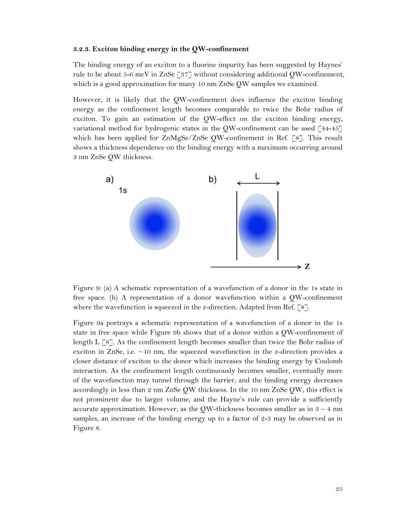
Figure 9: (a) A schematic representation of a wavefunction of a donor in the 1s state in free space. (b) A representation of a donor wavefunction within a QW-confinement where the wavefunction is squeezed in the z-direction. Adapted from Ref. [8].
Figure 9a portrays a schematic representation of a wavefunction of a donor in the 1s state in free space while Figure 9b shows that of a donor within a QW-confinement of length L [8]. As the confinement length becomes smaller than twice the Bohr radius of exciton in ZnSe, i.e. ~10 nm, the squeezed wavefunction in the z-direction provides a closer distance of exciton to the donor which increases the binding energy by Coulomb interaction. As the confinement length continuously becomes smaller, eventually more of the wavefunction may tunnel through the barrier, and the binding energy decreases accordingly in less than 2 nm ZnSe QW thickness. In the 10 nm ZnSe QW, this effect is not prominent due to larger volume, and the Hayne’s rule can provide a sufficiently accurate approximation. However, as the QW-thickness becomes smaller as in 3 – 4 nm samples, an increase of the binding energy up to a factor of 2-3 may be observed as in Figure 8.
26
3.3. Summary
In conclusion, introducing QW- confinement provides several advantages: Due to the double ZnMgSe cladding layers, carriers are prevented to leak into GaAs, but are more likely to fall into ZnSe QW-potential. This induces an enhanced optical brightness due to the increased radiative recombination rate in the active zone. Furthermore, an increased binding energy of exciton was observed because of the compression of the donor wavefunction in the QWs.
27
Chapter 4
Fluorine Doping of ZnSe
Although QDs based systems have already demonstrated several applications in quantum information science [16-17, 49-49], the small binding energies in most III-V semiconductors [50] elicit the isolation of single impurities challenging. Furthermore, their randomness in size and location causes substantial challenges for demonstrating sufficient homogeneity [17-18]. Semiconductor impurities provide a suitable ground for establishing a quantum system. Among group-VI systems, impurities in silicon show excellent homogeneity [51-52] but are optically dark inherited from the indirect band gap of Si.
Fluorine impurities in ZnSe (group II-VI) as argued in section 1.2 have advantages to compensate several challenges present in other systems. In chapter 2, the concepts of fluorine incorporation into ZnSe as donors were presented. In this chapter, experimental procedures and methodologies of doping fluorine in ZnSe will be extensively investigated. There are three primary fluorine doping methods which have been investigated throughout the courses of this thesis: 1) Fluorine doping during molecular beam epitaxy (MBE) without a cracker cell, 2) Fluorine doping during MBE growth assisted by a cracker cell. 3) Fluorine doping via ion implantation method.
4.1. Fluorine doping of ZnSe in the MBE The doping of fluorine is achieved simultaneously during the MBE growth of ZnMgSe/ZnSe QWs. A binary ZnF2 evaporation cell as shown in Figure 10a is equipped with a magnetic shutter few centimeters above the aperture of ZnF2 source, which can be precisely opened or closed in the milliseconds regime. Principally, the thermal energy provided by the furnace in the cell ought to dissociate fluorine from the ZnF2 establishing a gaseous molecular beam flux of fluorine. This molecular beam flux gives rise to a cosine intensity distribution with an extremely stable deposition rate, and the substrate is located at about zero-angle from the cell aperture for maximum intensity. The molecular beam flux of fluorine is controlled by
28
the temperature of the furnace which is accurately monitored with a proportional–integral–derivative controller (PID).
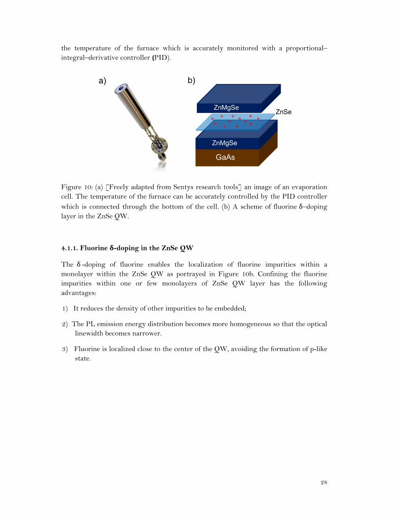
Figure 10: (a) [Freely adapted from Sentys research tools] an image of an evaporation cell. The temperature of the furnace can be accurately controlled by the PID controller which is connected through the bottom of the cell. (b) A scheme of fluorine δ–doping layer in the ZnSe QW.
4.1.1. Fluorine -doping in the ZnSe QW
The δ -doping of fluorine enables the localization of fluorine impurities within a monolayer within the ZnSe QW as portrayed in Figure 10b. Confining the fluorine impurities within one or few monolayers of ZnSe QW layer has the following advantages:
1) It reduces the density of other impurities to be embedded;
2) The PL emission energy distribution becomes more homogeneous so that the optical linewidth becomes narrower.
3) Fluorine is localized close to the center of the QW, avoiding the formation of p-like state.
29
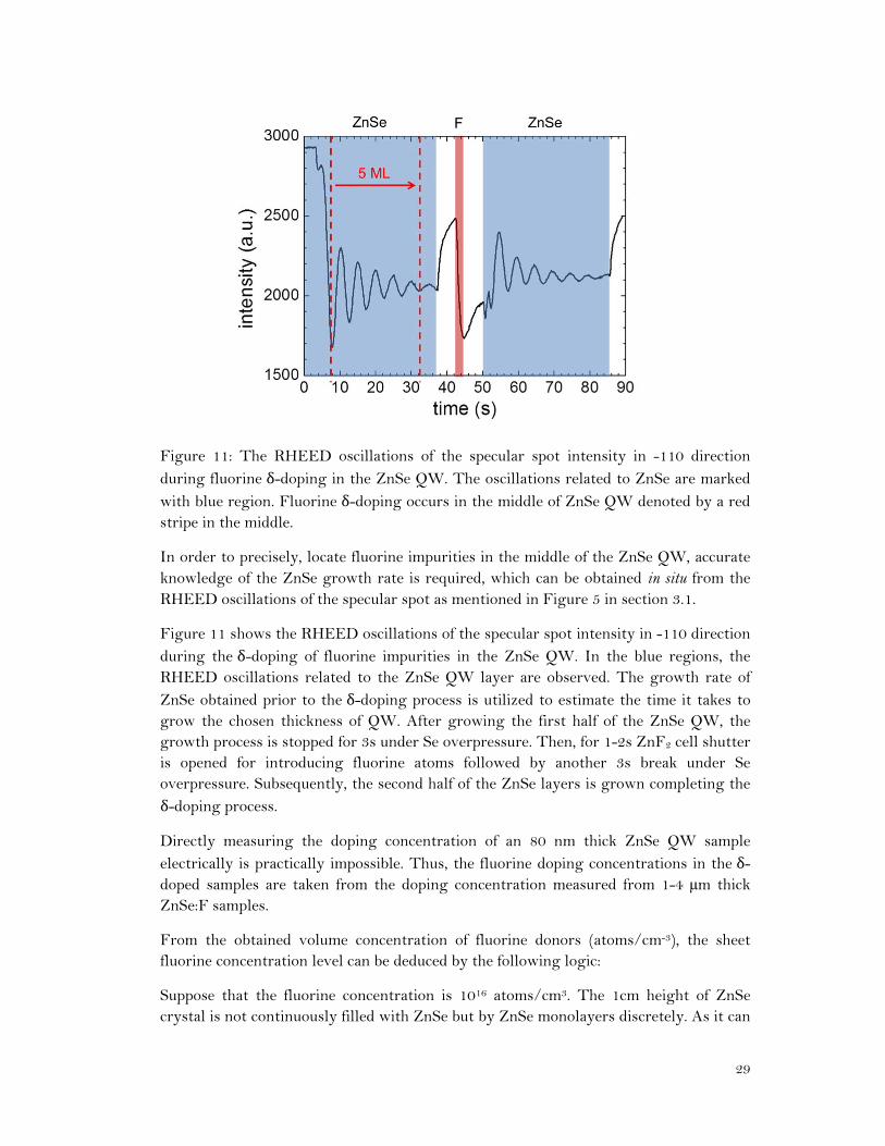
Figure 11: The RHEED oscillations of the specular spot intensity in -110 direction during fluorine δ-doping in the ZnSe QW. The oscillations related to ZnSe are marked
with blue region. Fluorine δ-doping occurs in the middle of ZnSe QW denoted by a red stripe in the middle.
In order to precisely, locate fluorine impurities in the middle of the ZnSe QW, accurate knowledge of the ZnSe growth rate is required, which can be obtained in situ from the RHEED oscillations of the specular spot as mentioned in Figure 5 in section 3.1.
Figure 11 shows the RHEED oscillations of the specular spot intensity in -110 direction during the δ-doping of fluorine impurities in the ZnSe QW. In the blue regions, the RHEED oscillations related to the ZnSe QW layer are observed. The growth rate of ZnSe obtained prior to the δ-doping process is utilized to estimate the time it takes to grow the chosen thickness of QW. After growing the first half of the ZnSe QW, the growth process is stopped for 3s under Se overpressure. Then, for 1-2s ZnF2 cell shutter is opened for introducing fluorine atoms followed by another 3s break under Se overpressure. Subsequently, the second half of the ZnSe layers is grown completing the δ-doping process.
Directly measuring the doping concentration of an 80 nm thick ZnSe QW sample electrically is practically impossible. Thus, the fluorine doping concentrations in the δ-doped samples are taken from the doping concentration measured from 1-4 μm thick ZnSe:F samples.
From the obtained volume concentration of fluorine donors (atoms/cm-3), the sheet fluorine concentration level can be deduced by the following logic:
Suppose that the fluorine concentration is 1016 atoms/cm3. The 1cm height of ZnSe crystal is not continuously filled with ZnSe but by ZnSe monolayers discretely. As it can
30
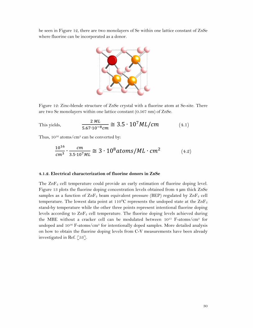
be seen in Figure 12, there are two monolayers of Se within one lattice constant of ZnSe where fluorine can be incorporated as a donor.
Figure 12: Zinc-blende structure of ZnSe crystal with a fluorine atom at Se-site. There are two Se monolayers within one lattice constant (0.567 nm) of ZnSe.
This yields,
. ∙≅ 3.5 ∙ 10 / (4.1)
Thus, 1016 atoms/cm3 can be converted by:
∙. ∙
≅ 3 ∙ 10 / ∙ (4.2)
4.1.2. Electrical characterization of fluorine donors in ZnSe
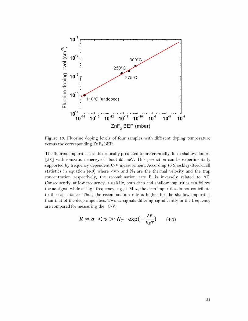
The ZnF2 cell temperature could provide an early estimation of fluorine doping level. Figure 13 plots the fluorine doping concentration levels obtained from 4 μm thick ZnSe samples as a function of ZnF2 beam equivalent pressure (BEP) regulated by ZnF2 cell temperature. The lowest data point at 110°C represents the undoped state at the ZnF2 stand-by temperature while the other three points represent intentional fluorine doping levels according to ZnF2 cell temperature. The fluorine doping levels achieved during the MBE without a cracker cell can be modulated between 1015 F-atoms/cm3 for undoped and 1016 F-atoms/cm3 for intentionally doped samples. More detailed analysis on how to obtain the fluorine doping levels from C-V measurements have been already investigated in Ref. [53].
31
Figure 13: Fluorine doping levels of four samples with different doping temperature versus the corresponding ZnF2 BEP.
The fluorine impurities are theoretically predicted to preferentially, form shallow donors [38] with ionization energy of about 29 meV. This prediction can be experimentally supported by frequency dependent C-V measurement. According to Shockley-Reed-Hall statistics in equation (4.3) where <v> and NT are the thermal velocity and the trap concentration respectively, the recombination rate R is inversely related to ΔE. Consequently, at low frequency; <10 kHz, both deep and shallow impurities can follow the ac signal while at high frequency, e.g., 1 Mhz, the deep impurities do not contribute to the capacitance. Thus, the recombination rate is higher for the shallow impurities than that of the deep impurities. Two ac signals differing significantly in the frequency are compared for measuring the C-V.
∙ ∙ ∙ exp ∆ (4.3)
32
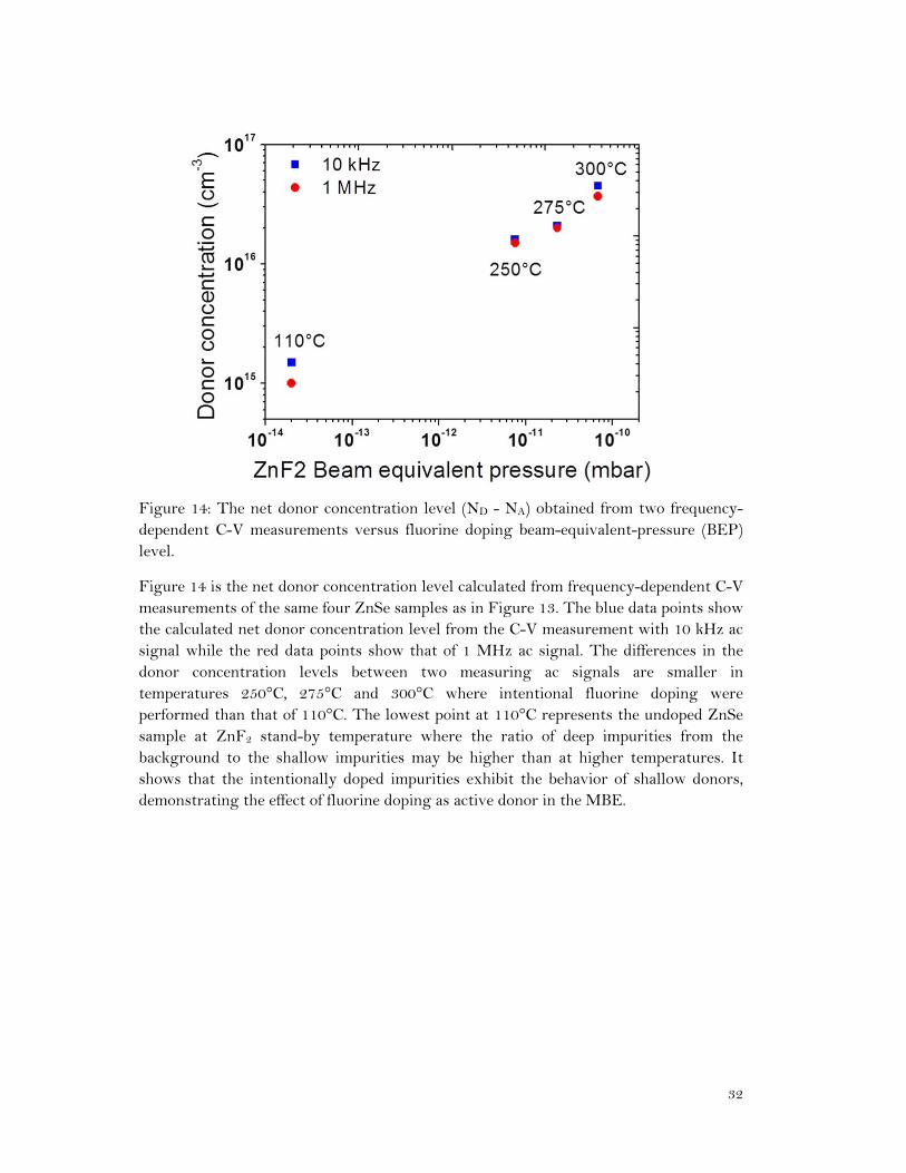
Figure 14: The net donor concentration level (ND - NA) obtained from two frequency-dependent C-V measurements versus fluorine doping beam-equivalent-pressure (BEP) level.
Figure 14 is the net donor concentration level calculated from frequency-dependent C-V measurements of the same four ZnSe samples as in Figure 13. The blue data points show the calculated net donor concentration level from the C-V measurement with 10 kHz ac signal while the red data points show that of 1 MHz ac signal. The differences in the donor concentration levels between two measuring ac signals are smaller in temperatures 250°C, 275°C and 300°C where intentional fluorine doping were performed than that of 110°C. The lowest point at 110°C represents the undoped ZnSe sample at ZnF2 stand-by temperature where the ratio of deep impurities from the background to the shallow impurities may be higher than at higher temperatures. It shows that the intentionally doped impurities exhibit the behavior of shallow donors, demonstrating the effect of fluorine doping as active donor in the MBE.
33
4.1.3. Optical characterization of fluorine donors in ZnSe
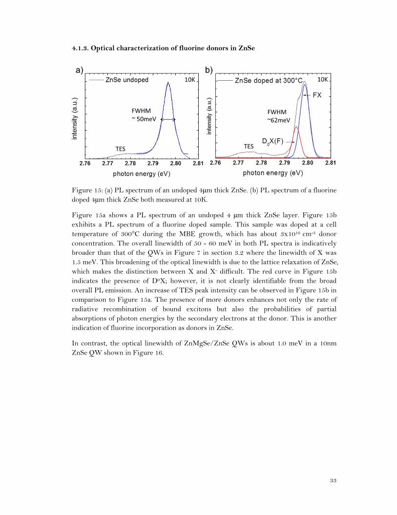
Figure 15: (a) PL spectrum of an undoped 4μm thick ZnSe. (b) PL spectrum of a fluorine doped 4μm thick ZnSe both measured at 10K.
Figure 15a shows a PL spectrum of an undoped 4 μm thick ZnSe layer. Figure 15b exhibits a PL spectrum of a fluorine doped sample. This sample was doped at a cell temperature of 300°C during the MBE growth, which has about 3x1016 cm-3 donor concentration. The overall linewidth of 50 - 60 meV in both PL spectra is indicatively broader than that of the QWs in Figure 7 in section 3.2 where the linewidth of X was 1.5 meV. This broadening of the optical linewidth is due to the lattice relaxation of ZnSe, which makes the distinction between X and X- difficult. The red curve in Figure 15b indicates the presence of D0X; however, it is not clearly identifiable from the broad overall PL emission. An increase of TES peak intensity can be observed in Figure 15b in comparison to Figure 15a. The presence of more donors enhances not only the rate of radiative recombination of bound excitons but also the probabilities of partial absorptions of photon energies by the secondary electrons at the donor. This is another indication of fluorine incorporation as donors in ZnSe.
In contrast, the optical linewidth of ZnMgSe/ZnSe QWs is about 1.0 meV in a 10nm ZnSe QW shown in Figure 16.
34
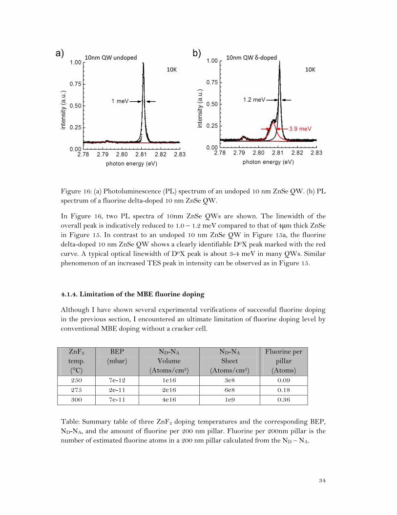
Figure 16: (a) Photoluminescence (PL) spectrum of an undoped 10 nm ZnSe QW. (b) PL spectrum of a fluorine delta-doped 10 nm ZnSe QW.
In Figure 16, two PL spectra of 10nm ZnSe QWs are shown. The linewidth of the overall peak is indicatively reduced to 1.0 – 1.2 meV compared to that of 4μm thick ZnSe in Figure 15. In contrast to an undoped 10 nm ZnSe QW in Figure 15a, the fluorine delta-doped 10 nm ZnSe QW shows a clearly identifiable D0X peak marked with the red curve. A typical optical linewidth of D0X peak is about 3-4 meV in many QWs. Similar phenomenon of an increased TES peak in intensity can be observed as in Figure 15.
4.1.4. Limitation of the MBE fluorine doping
Although I have shown several experimental verifications of successful fluorine doping in the previous section, I encountered an ultimate limitation of fluorine doping level by conventional MBE doping without a cracker cell.
Table: Summary table of three ZnF2 doping temperatures and the corresponding BEP, ND-NA, and the amount of fluorine per 200 nm pillar. Fluorine per 200nm pillar is the number of estimated fluorine atoms in a 200 nm pillar calculated from the ND – NA.
ZnF2 temp. (°C)
BEP (mbar)
ND-NA Volume
(Atoms/cm3)
ND-NA Sheet
(Atoms/cm3)
Fluorine per pillar
(Atoms) 250 7e-12 1e16 3e8 0.09 275 2e-11 2e16 6e8 0.18 300 7e-11 4e16 1e9 0.36
35
The table above is a brief summary of three ZnF2 doping temperatures and the corresponding BEP, ND-NA in volume and sheet, and the amount of fluorine atoms within a 200 nm diameter pillar. Fluorine within a 200nm pillar is the number of estimated fluorine atoms in a 200 nm pillar structure as calculated from the ND – NA. The calculation of the fluorine per pillar is obtained by dividing the fluorine sheet concentration with the cross-section area of a 100nm radius circle. Ideally, having one fluorine impurity per pillar is desired. However, as seen in the table above, at 300°C doping temperature, the number of fluorine atoms per 200 nm pillars is still about 1/3. It implies that the ND – NA must achieve 1017 cm-3 at minimum. However, our experimental experiences have shown that at higher doping temperature over 350°C, the total ZnF2 flux began to dominate so that the ZnF2 crystal formation was observed. It suggests that the applied thermal energy from the furnace of ZnF2 cell have not been enough to dissociate sufficient 19F from ZnF2; thus only a small amount of the separated 19F atoms were involved in the doping process. These results communicate the message that with conventional MBE fluorine doping method, one cannot achieve the necessary doping concentration level. Implementing a cracker for further separating fluorine atoms could improve the doping level which will be discussed in the next section.
4.2. MBE doping of fluorine in ZnSe with a cracker cell
4.2.1. Thermal dissociation of ZnF2 by a cracker cell
The conventional MBE fluorine doping discussed in the previous section was found insufficient to achieve a sheet donor concentration level beyond 1016 cm-3. Here, we investigate the MBE doping process of fluorine in ZnSe assisted with a ZnF2 cracker cell and the improved results. A cracker cell can provide sufficient thermal energy for dissociating all ZnF2 molecules passing through the cracker at the exit-point. The outlet diameter of our cracker-cell is about 2-3 mm which is smaller than a regular evaporation cell, which is about few centimeters. The molecules are temporarily trapped or delayed through an elongated path, which is often cylindrical at the exit-point. The second heater, i.e., the cracker is set to a higher temperature than the source, and through this additional thermal work, the molecules are dissociated into individual atoms before they escape to the chamber.
36
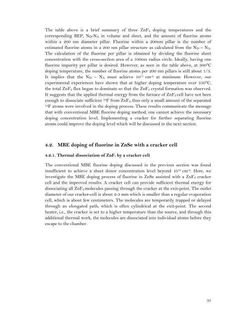
Figure 17: (a) An installed fluorine cracker cell in our MBE chamber. (b) Inside view of the chamber when the cracker cell is in operation.
Figure 17a shows the installed cracker cell in our MBE chamber, and 17b shows the glowing image of the cracker cell in operation. The cylindrical path which delays the exit of ZnF2 molecules is visible inside. The second heater is seen which surrounds the exit-point of the cell. The calibration of the cell is an essential step prior to operating the cell for doping. The real cell temperature and the arbitrary temperature scale in measurement must be calibrated. This can be achieved by comparing the output current with the cell temperature.
After the calibration, a mass-spectrometer installed in the MBE chamber was used to measure the rate of fluorine dissociation versus temperature. By a mass-spectrometer, the total BEP can be separated by atomic mass, which allows us to estimate the contribution of fluorine-related molecular species in relation to the reservoir temperature. The cracker temperature was constantly kept at 920°C while the reservoir temperature was varied between 600°C to 800°C.
37
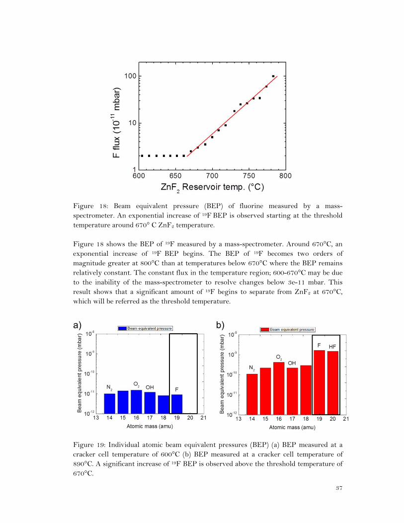
Figure 18: Beam equivalent pressure (BEP) of fluorine measured by a mass-spectrometer. An exponential increase of 19F BEP is observed starting at the threshold temperature around 670° C ZnF2 temperature. Figure 18 shows the BEP of 19F measured by a mass-spectrometer. Around 670°C, an exponential increase of 19F BEP begins. The BEP of 19F becomes two orders of magnitude greater at 800°C than at temperatures below 670°C where the BEP remains relatively constant. The constant flux in the temperature region; 600-670°C may be due to the inability of the mass-spectrometer to resolve changes below 3e-11 mbar. This result shows that a significant amount of 19F begins to separate from ZnF2 at 670°C, which will be referred as the threshold temperature.
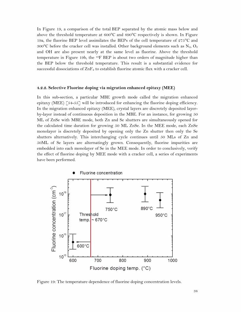
Figure 19: Individual atomic beam equivalent pressures (BEP) (a) BEP measured at a cracker cell temperature of 600°C (b) BEP measured at a cracker cell temperature of 890°C. A significant increase of 19F BEP is observed above the threshold temperature of 670°C.
38
In Figure 19, a comparison of the total BEP separated by the atomic mass below and above the threshold temperature at 600°C and 890°C respectively is shown. In Figure 19a, the fluorine BEP level assimilates the BEPs of the cell temperature of 275°C and 300°C before the cracker cell was installed. Other background elements such as N2, O2 and OH are also present nearly at the same level as fluorine. Above the threshold temperature in Figure 19b, the 19F BEP is about two orders of magnitude higher than the BEP below the threshold temperature. This result is a substantial evidence for successful dissociations of ZnF2 to establish fluorine atomic flux with a cracker cell.
4.2.2. Selective Fluorine doping via migration enhanced epitaxy (MEE)
In this sub-section, a particular MBE growth mode called the migration enhanced epitaxy (MEE) [54-55] will be introduced for enhancing the fluorine doping efficiency. In the migration enhanced epitaxy (MEE), crystal layers are discretely deposited layer-by-layer instead of continuous deposition in the MBE. For an instance, for growing 50 ML of ZnSe with MBE mode, both Zn and Se shutters are simultaneously opened for the calculated time duration for growing 50 ML ZnSe. In the MEE mode, each ZnSe monolayer is discretely deposited by opening only the Zn shutter then only the Se shutters alternatively. This interchanging cycle continues until 50 MLs of Zn and 50ML of Se layers are alternatingly grown. Consequently, fluorine impurities are embedded into each monolayer of Se in the MEE mode. In order to conclusively, verify the effect of fluorine doping by MEE mode with a cracker cell, a series of experiments have been performed.
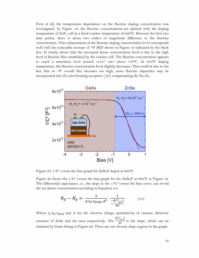
Figure 19: The temperature dependence of fluorine doping concentration levels.
39
First of all, the temperature dependence on the fluorine doping concentration was investigated. In Figure 19, the fluorine concentrations are plotted with the doping temperature of ZnF2 cell at a fixed cracker temperature of 920°C. Between the first two data points, there is about two orders of magnitude difference in the fluorine concentration. This enhancement of the fluorine doping concentration level corresponds well with the noticeable increase of 19F BEP shown in Figure 19 indicated by the black box. It clearly shows that the increased donor concentration level is due to the high level of fluorine flux established by the cracker cell. The fluorine concentration appears to reach a saturation level around 1x1018 cm-3 above 750°C. At 950°C doping temperature, the fluorine concentration level slightly decreases. This could be due to the fact that as 19F overall flux becomes too high, more fluorine impurities may be incorporated into Zn sites forming acceptors [40] compensating the ND-NA.
Figure 20: 1/C2 versus the bias graph for ZnSe:F doped at 600°C.
Figure 20 shows the 1/C2 versus the bias graph for the ZnSe:F at 600°C in Figure 19. The differential capacitance, i.e., the slope in the 1/C2 versus the bias curve, can reveal the net donor concentration according to Equation 4.4.
∙ ∙ ∙
∙ (4.4)
Where q, , and A are the electron charge, permittivity of vacuum, dielectric
constant of ZnSe and the area respectively. The is the slope, which can be
obtained by linear fitting in Figure 20. There are two diverse slope regions in the graph.
40
The 1x1018 cm-3 region in brown is the n-GaAs substrate and the 5x1015 cm-3 region in blue is ZnSe:F. The depletion width which is inversely proportional to the capacitance, reveals that ZnSe:F region is within 500 nm depth from the surface.
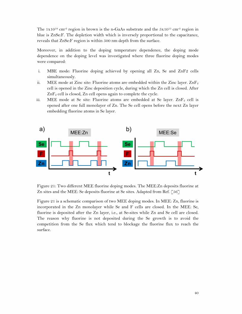
Moreover, in addition to the doping temperature dependence, the doping mode dependence on the doping level was investigated where three fluorine doping modes were compared:
i. MBE mode: Fluorine doping achieved by opening all Zn, Se and ZnF2 cells simultaneously.
ii. MEE mode at Zinc site: Fluorine atoms are embedded within the Zinc layer. ZnF2 cell is opened in the Zinc deposition cycle, during which the Zn cell is closed. After ZnF2 cell is closed, Zn cell opens again to complete the cycle.
iii. MEE mode at Se site: Fluorine atoms are embedded at Se layer. ZnF2 cell is opened after one full monolayer of Zn. The Se cell opens before the next Zn layer embedding fluorine atoms in Se layer.
Figure 21: Two different MEE fluorine doping modes. The MEE:Zn deposits fluorine at Zn sites and the MEE: Se deposits fluorine at Se sites. Adapted from Ref. [56]
Figure 21 is a schematic comparison of two MEE doping modes. In MEE: Zn, fluorine is incorporated in the Zn monolayer while Se and F cells are closed. In the MEE: Se, fluorine is deposited after the Zn layer, i.e., at Se-sites while Zn and Se cell are closed. The reason why fluorine is not deposited during the Se growth is to avoid the competition from the Se flux which tend to blockage the fluorine flux to reach the surface.
41
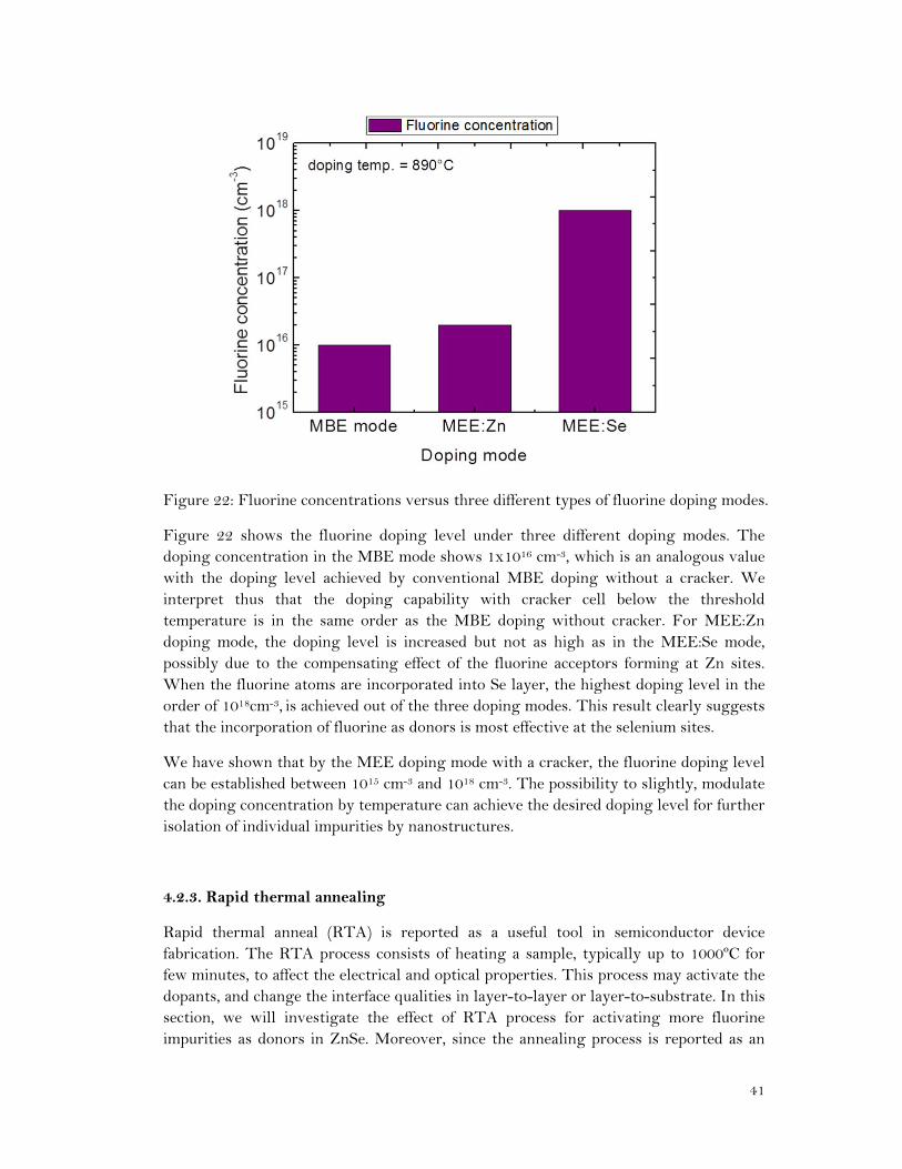
Figure 22: Fluorine concentrations versus three different types of fluorine doping modes.
Figure 22 shows the fluorine doping level under three different doping modes. The doping concentration in the MBE mode shows 1x1016 cm-3, which is an analogous value with the doping level achieved by conventional MBE doping without a cracker. We interpret thus that the doping capability with cracker cell below the threshold temperature is in the same order as the MBE doping without cracker. For MEE:Zn doping mode, the doping level is increased but not as high as in the MEE:Se mode, possibly due to the compensating effect of the fluorine acceptors forming at Zn sites. When the fluorine atoms are incorporated into Se layer, the highest doping level in the order of 1018cm-3, is achieved out of the three doping modes. This result clearly suggests that the incorporation of fluorine as donors is most effective at the selenium sites.
We have shown that by the MEE doping mode with a cracker, the fluorine doping level can be established between 1015 cm-3 and 1018 cm-3. The possibility to slightly, modulate the doping concentration by temperature can achieve the desired doping level for further isolation of individual impurities by nanostructures.
4.2.3. Rapid thermal annealing
Rapid thermal anneal (RTA) is reported as a useful tool in semiconductor device fabrication. The RTA process consists of heating a sample, typically up to 1000ºC for few minutes, to affect the electrical and optical properties. This process may activate the dopants, and change the interface qualities in layer-to-layer or layer-to-substrate. In this section, we will investigate the effect of RTA process for activating more fluorine impurities as donors in ZnSe. Moreover, since the annealing process is reported as an
42
important factor for post-treatment of semiconductor devices with ion implantation [57], the same process can also be applied to the ion implanted samples for repairing the implantation damage.
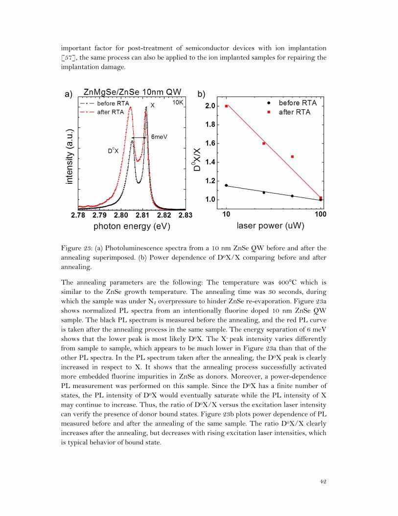
Figure 23: (a) Photoluminescence spectra from a 10 nm ZnSe QW before and after the annealing superimposed. (b) Power dependence of D0X/X comparing before and after annealing.
The annealing parameters are the following: The temperature was 400°C which is similar to the ZnSe growth temperature. The annealing time was 30 seconds, during which the sample was under N2 overpressure to hinder ZnSe re-evaporation. Figure 23a shows normalized PL spectra from an intentionally fluorine doped 10 nm ZnSe QW sample. The black PL spectrum is measured before the annealing, and the red PL curve is taken after the annealing process in the same sample. The energy separation of 6 meV shows that the lower peak is most likely D0X. The X- peak intensity varies differently from sample to sample, which appears to be much lower in Figure 23a than that of the other PL spectra. In the PL spectrum taken after the annealing, the D0X peak is clearly increased in respect to X. It shows that the annealing process successfully activated more embedded fluorine impurities in ZnSe as donors. Moreover, a power-dependence PL measurement was performed on this sample. Since the D0X has a finite number of states, the PL intensity of D0X would eventually saturate while the PL intensity of X may continue to increase. Thus, the ratio of D0X/X versus the excitation laser intensity can verify the presence of donor bound states. Figure 23b plots power dependence of PL measured before and after the annealing of the same sample. The ratio D0X/X clearly increases after the annealing, but decreases with rising excitation laser intensities, which is typical behavior of bound state.
43
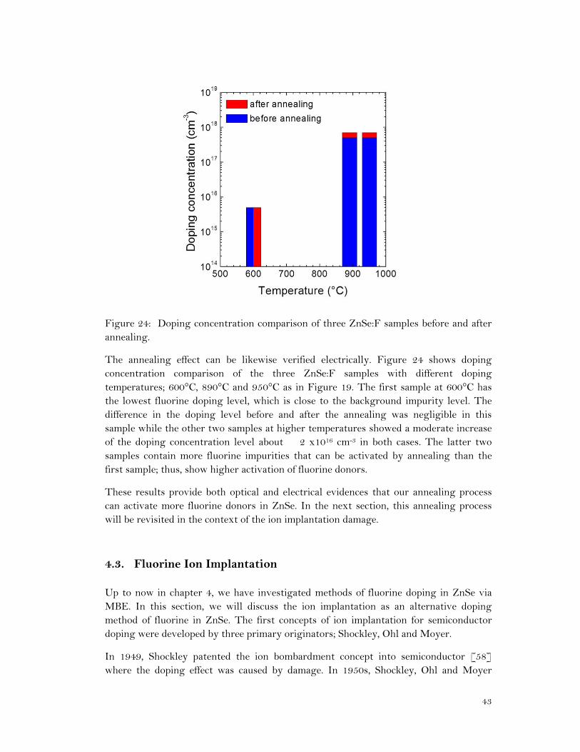
Figure 24: Doping concentration comparison of three ZnSe:F samples before and after annealing.
The annealing effect can be likewise verified electrically. Figure 24 shows doping concentration comparison of the three ZnSe:F samples with different doping temperatures; 600°C, 890°C and 950°C as in Figure 19. The first sample at 600°C has the lowest fluorine doping level, which is close to the background impurity level. The difference in the doping level before and after the annealing was negligible in this sample while the other two samples at higher temperatures showed a moderate increase of the doping concentration level about 2 x1016 cm-3 in both cases. The latter two samples contain more fluorine impurities that can be activated by annealing than the first sample; thus, show higher activation of fluorine donors.
These results provide both optical and electrical evidences that our annealing process can activate more fluorine donors in ZnSe. In the next section, this annealing process will be revisited in the context of the ion implantation damage.
4.3. Fluorine Ion Implantation Up to now in chapter 4, we have investigated methods of fluorine doping in ZnSe via MBE. In this section, we will discuss the ion implantation as an alternative doping method of fluorine in ZnSe. The first concepts of ion implantation for semiconductor doping were developed by three primary originators; Shockley, Ohl and Moyer.
In 1949, Shockley patented the ion bombardment concept into semiconductor [58] where the doping effect was caused by damage. In 1950s, Shockley, Ohl and Moyer
44
further contributed to the realization of ion implantation; with surface modification by Ohl [59] and with implanted atoms beneath the surface into bulk semiconductors by Moyer and Shockley [60-61]. This method became commercially available in 1973. In the same year, the ion implantation of Li ions in ZnSe was reported [62] and the first ion implantation of fluorine into single ZnSe crystal as donors was published in 1978[63]. At that time, the interests in the group II-VI semiconductor compounds were high for their light emitting properties in the green and blue spectral range as LEDs or LDs. However, the vulnerability under high current or high power conditions observed in the II-VI compounds turned the tide of research interests away to other materials such as GaN in group III-V. Throughout my thesis, I have attempted to demonstrate the properties of fluorine impurities in ZnSe not for optical device application but for applications in quantum information science schemes. Here, I will present the ion implantation of fluorine in ZnSe QWs for quantum information science purposes.
4.3.1. Mechanism of ion implantation
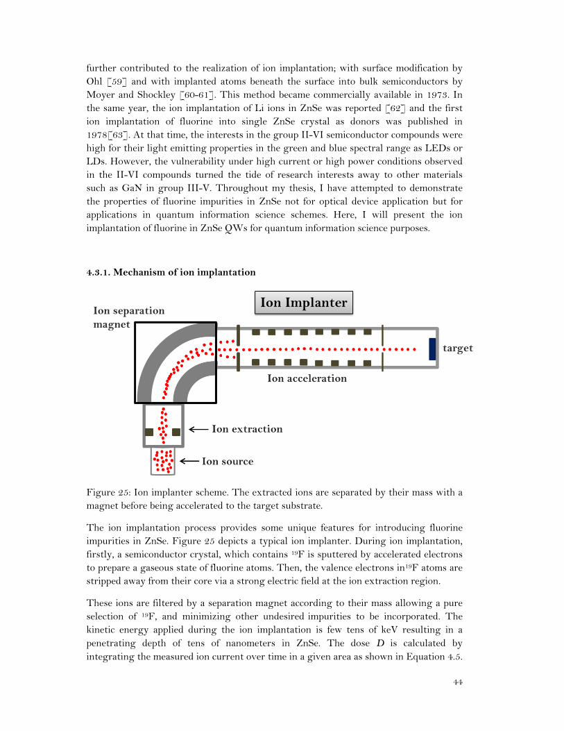
Figure 25: Ion implanter scheme. The extracted ions are separated by their mass with a magnet before being accelerated to the target substrate.
The ion implantation process provides some unique features for introducing fluorine impurities in ZnSe. Figure 25 depicts a typical ion implanter. During ion implantation, firstly, a semiconductor crystal, which contains 19F is sputtered by accelerated electrons to prepare a gaseous state of fluorine atoms. Then, the valence electrons in19F atoms are stripped away from their core via a strong electric field at the ion extraction region.
These ions are filtered by a separation magnet according to their mass allowing a pure selection of 19F, and minimizing other undesired impurities to be incorporated. The kinetic energy applied during the ion implantation is few tens of keV resulting in a penetrating depth of tens of nanometers in ZnSe. The dose D is calculated by integrating the measured ion current over time in a given area as shown in Equation 4.5.
45
This ion current can be precisely set during the implantation, and can be varied in a wide range. In our case, we varied the dose in a range of 109 - 1013 fluorine atoms per cm2, which is in volume equivalent to 1016 – 1020 cm-3. Since the dose can be precisely set by the current during the implantation, the doping level is more discretely controllable than in the MBE doping. In the previous section regarding MEE doping with a cracker, we reported a doping range between 1015 cm-3 and 1018 cm-3, but the intermediate doping levels cannot be discretely controlled as in the ion implantation.
D∙
(4.5)
Moreover, localized doping is available by selective implantation through a several nanometer sized mask or Atomic Force Microscope (AFM) tips which is otherwise extremely difficult in the purely MBE processes [64-65]. Furthermore, the possibility of implanting countable single ions on a nanometer scale has been shown for highly charged 31P2+ ions [66] or by using ion traps [67-68], which may also be possible for fluorine. These unique features of ion implantation may allow a combination of the MBE process for growth and the selective implantation of fluorine as doping mechanism for constructing single photon sources (SPS).
The local concentration of implanted ions as a function of depth z can be numerically simulated by Monte Carlo method. The LSS theory can also be used as an analytical tool to calculate the local concentration [69].
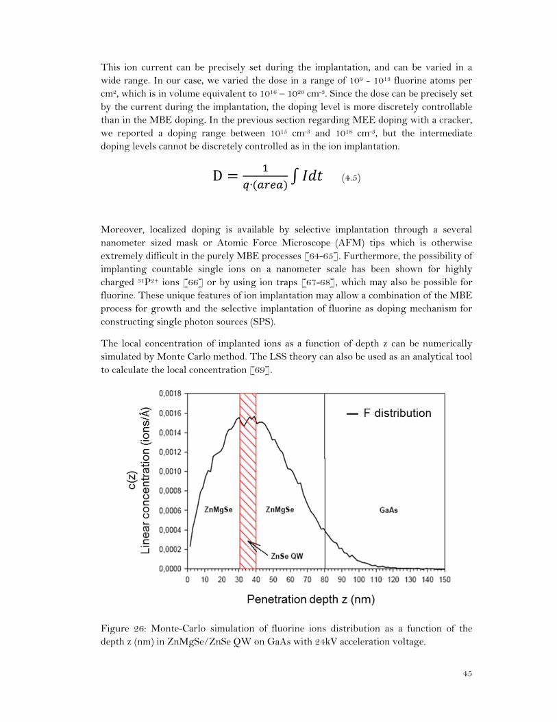
Figure 26: Monte-Carlo simulation of fluorine ions distribution as a function of the depth z (nm) in ZnMgSe/ZnSe QW on GaAs with 24kV acceleration voltage.
46
Figure 26 shows a Monte-Carlo simulation of fluorine ions distribution as a function of penetrating depth z (nm) in ZnMgSe/ZnSe 10 nm QW. For this simulation, an acceleration voltage of 24kV was chosen. This simulation is attributed to the group of Prof. Jörg Lindner in the University of Paderborn. The linear concentration c(z) is defined as the number of fluorine atoms or ions per angstrom. The 24kV acceleration voltage was chosen such that the maximum distribution is located nearly in the middle of the QW width. Unlike in the MBE doping, the δ-doping is not possible since the ions are externally introduced from the surface and are randomly distributed in purely statistical manner.
4.3.2. Selective ion implantation
In order to verify the selective ion implantation, the following experiment was carried out.
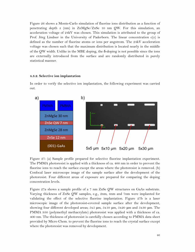
Figure 27: (a) Sample profile prepared for selective fluorine implantation experiment. The PMMA photoresist is applied with a thickness of ca. 400 nm in order to prevent the fluorine ions to reach the surface except the areas where the photoresist is removed. (b) Confocal laser microscope image of the sample surface after the development of the photoresist. Four different areas of exposure are prepared for comparing the doping concentration levels.
Figure 27a shows a sample profile of a 7 nm ZnSe QW structures on GaAs substrate. Varying thickness of ZnSe QW samples, e.g., 2nm, 4nm and 7nm were implanted for validating the effect of the selective fluorine implantation. Figure 27b is a laser microscopic image of the photoresist-covered sample surface after the development, showing four different developed areas; 5x5 μm, 5x10 μm, 5x20 μm and 5x30 μm. The PMMA 950 (polymethyl methacrylate) photoresist was applied with a thickness of ca. 400 nm. The thickness of photoresist is carefully chosen according to PMMA data sheet provided by Micro Chem. to prevent the fluorine ions to reach the crystal surface except where the photoresist was removed by development.
47
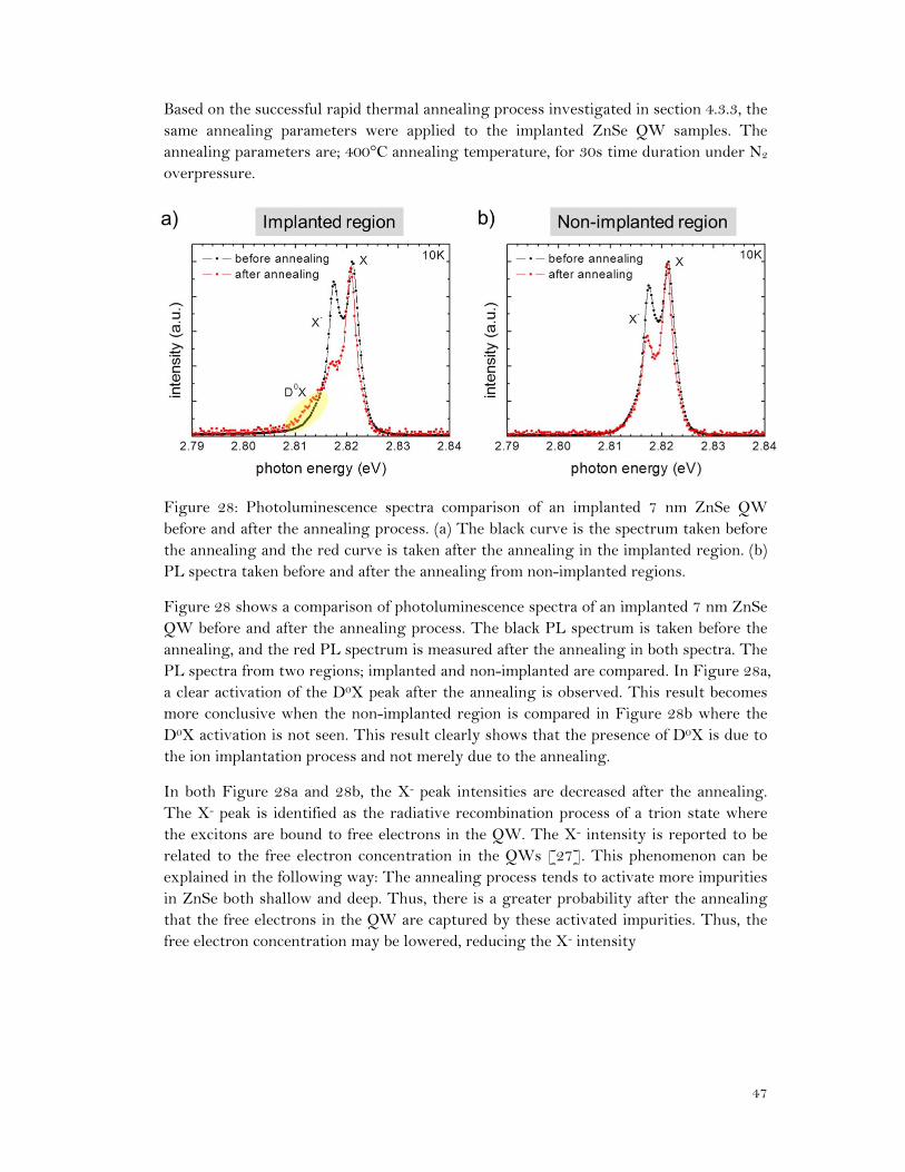
Based on the successful rapid thermal annealing process investigated in section 4.3.3, the same annealing parameters were applied to the implanted ZnSe QW samples. The annealing parameters are; 400°C annealing temperature, for 30s time duration under N2 overpressure.
Figure 28: Photoluminescence spectra comparison of an implanted 7 nm ZnSe QW before and after the annealing process. (a) The black curve is the spectrum taken before the annealing and the red curve is taken after the annealing in the implanted region. (b) PL spectra taken before and after the annealing from non-implanted regions.
Figure 28 shows a comparison of photoluminescence spectra of an implanted 7 nm ZnSe QW before and after the annealing process. The black PL spectrum is taken before the annealing, and the red PL spectrum is measured after the annealing in both spectra. The PL spectra from two regions; implanted and non-implanted are compared. In Figure 28a, a clear activation of the D0X peak after the annealing is observed. This result becomes more conclusive when the non-implanted region is compared in Figure 28b where the D0X activation is not seen. This result clearly shows that the presence of D0X is due to the ion implantation process and not merely due to the annealing.
In both Figure 28a and 28b, the X- peak intensities are decreased after the annealing. The X- peak is identified as the radiative recombination process of a trion state where the excitons are bound to free electrons in the QW. The X- intensity is reported to be related to the free electron concentration in the QWs [27]. This phenomenon can be explained in the following way: The annealing process tends to activate more impurities in ZnSe both shallow and deep. Thus, there is a greater probability after the annealing that the free electrons in the QW are captured by these activated impurities. Thus, the free electron concentration may be lowered, reducing the X- intensity
48
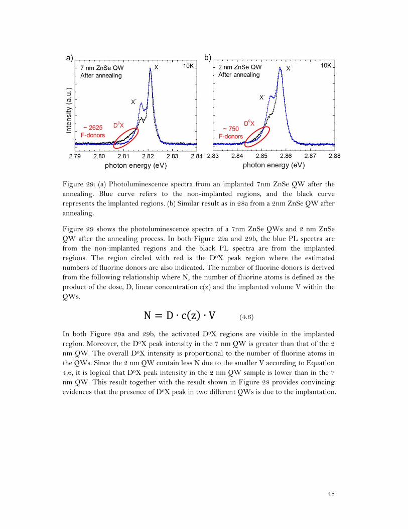
Figure 29: (a) Photoluminescence spectra from an implanted 7nm ZnSe QW after the annealing. Blue curve refers to the non-implanted regions, and the black curve represents the implanted regions. (b) Similar result as in 28a from a 2nm ZnSe QW after annealing.
Figure 29 shows the photoluminescence spectra of a 7nm ZnSe QWs and 2 nm ZnSe QW after the annealing process. In both Figure 29a and 29b, the blue PL spectra are from the non-implanted regions and the black PL spectra are from the implanted regions. The region circled with red is the D0X peak region where the estimated numbers of fluorine donors are also indicated. The number of fluorine donors is derived from the following relationship where N, the number of fluorine atoms is defined as the product of the dose, D, linear concentration c(z) and the implanted volume V within the QWs.
N D ∙ c z ∙ V (4.6)
In both Figure 29a and 29b, the activated D0X regions are visible in the implanted region. Moreover, the D0X peak intensity in the 7 nm QW is greater than that of the 2 nm QW. The overall D0X intensity is proportional to the number of fluorine atoms in the QWs. Since the 2 nm QW contain less N due to the smaller V according to Equation 4.6, it is logical that D0X peak intensity in the 2 nm QW sample is lower than in the 7 nm QW. This result together with the result shown in Figure 28 provides convincing evidences that the presence of D0X peak in two different QWs is due to the implantation.
49
4.4. Summary
We investigated the MBE doping method of fluorine and verified the doping effects by electrical and optical characterizations. The fluorine concentration levels achieved with the conventional MBE doping are limited to 1016 cm-3 most likely due to the insufficient thermal dissociation of ZnF2. In section 4.2, the ZnF2 cracker cell was introduced which enabled successful dissociation of ZnF2, establishing 19F molecular beam flux. The significant enhancement of the 19F BEP levels by two orders of magnitude strongly correlates with the increased fluorine doping concentration in the intentionally doped samples. The comparison of the fluorine doping levels by doping temperature and the doping modes suggests that the fluorine doping levels can be modulated between 1015 cm-3 and 1018 cm-3. Furthermore, we have investigated the ion implantation of fluorine in ZnSe as an alternative doping method. With appropriate annealing processes, the fluorine impurities can be successfully incorporated as donors in ZnSe QWs. The unique features that the ion implantation can provide; 1) the pure selection of 19F avoiding other non-desired elements, 2) more precise doping level control, 3) selective ion implantation, and 4) possibly registrations of single ions, make the ion implantation of fluorine in ZnSe an attractive tool for quantum information science applications.

50
51
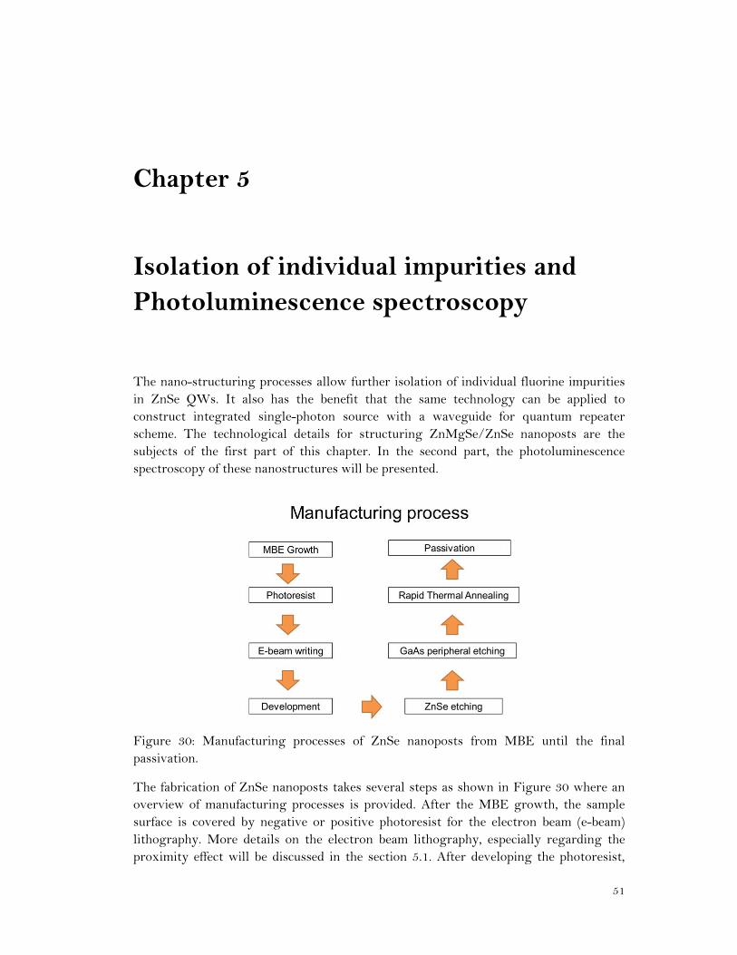
Chapter 5
Isolation of individual impurities and Photoluminescence spectroscopy
The nano-structuring processes allow further isolation of individual fluorine impurities in ZnSe QWs. It also has the benefit that the same technology can be applied to construct integrated single-photon source with a waveguide for quantum repeater scheme. The technological details for structuring ZnMgSe/ZnSe nanoposts are the subjects of the first part of this chapter. In the second part, the photoluminescence spectroscopy of these nanostructures will be presented.
Figure 30: Manufacturing processes of ZnSe nanoposts from MBE until the final passivation.
The fabrication of ZnSe nanoposts takes several steps as shown in Figure 30 where an overview of manufacturing processes is provided. After the MBE growth, the sample surface is covered by negative or positive photoresist for the electron beam (e-beam) lithography. More details on the electron beam lithography, especially regarding the proximity effect will be discussed in the section 5.1. After developing the photoresist,
52
the sample is ready for the etching process. For the most part of this thesis, the wet-chemical etching of ZnSe by Potassium dichromate (K2Cr2O7) solution was utilized for superior optical quality to the dry-etching via Reactive Ion Etching (RIE) process. The surface oxidation of ZnSe under air is a well-known issue [70], and the importance of its treatment will be discussed in 5.1.2. After the etching, rapid thermal annealing process is carried out as reported in Section 4.3. At last, the passivation process by either SiO2 or Si3N4 completes the manufacturing of ZnMgSe/ZnSe nanoposts. The purposes for passivation are: to restrain relaxation, to avoid further oxidation, and to protect the sample surface from breaking due to thermal expansion during the cooling and warming cycle. There has been no significant difference observed between the two passivation materials, thus the readers could assume that the investigated samples are passivated by SiO2 unless otherwise mentioned. All recipes of the above manufacturing processes are summarized in the Appendix B.
5.1. Fabrication of ZnMgSe/ZnSe nanoposts
5.1.1. Electron beam lithography
Electron beam (e-beam) lithography as the name conveys is an analogous process as the photolithography but with an electron beam exposure. Primarily, e-beam lithography involves two steps; to pattern the structures on photoresist with electron beams, and to develop the photoresist. One key advantage of the e-beam lithography is its superior resolution to the diffraction limit in the photolithography; hundreds of nanometers. The resolution of e-beam lithography is typically limited to 10 - 30 nanometers due to the electron optics in the instrument, and the electron backscattering effect, which will be discussed in the following section. Throughout the courses of this thesis, two scanning electron microscopes (SEM) were used. The first SEM is JEOL 5610-LV model whose primary function is surface imaging, features an acceleration voltage in a range between 0.6 – 30.0 kV. The spatial resolution limit is about 30 nm and the lithography limit on ZnSe is around 50 - 100 nm. It facilitates the secondary electron images operated under high vacuum condition with maximum magnification up to 120,000x.
The second SEM made available towards the end of this thesis is Raith Pioneer with much superior resolution. The lithography limit on Raith Pioneer is around 10 nm with maximum magnification up to 500,000x. It facilitates both an in-line detector directly above the sample and the secondary electron detector at the side.
For patterning nanoposts, ma-N 2403 negative resist from micro resist technology was used. The covering of the sample surface with photoresist involves few steps. First, the thickness of the resist must be chosen for the structure size according to the negative photoresist data sheet found in the Appendix B. For 200 nm diameter pillars on ZnSe, 4000 rpm for 30s rotation is appropriate for having the photoresist thickness between 180 – 200 nm. After the spinning process, 60s of bake out on 90°C hot plate is followed for hardening the resist surface. Subsequently, individual pillars and the markers are
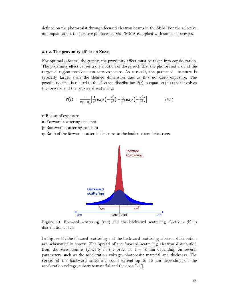
53
defined on the photoresist through focused electron beams in the SEM. For the selective ion implantation, the positive photoresist 950 PMMA is applied with similar processes.
5.1.2. The proximity effect on ZnSe
For optimal e-beam lithography, the proximity effect must be taken into consideration. The proximity effect causes a distribution of doses such that the photoresist around the targeted region receives non-zero exposure. As a result, the patterned structure is typically larger than the defined dimension due to this non-zero exposure. The proximity effect is related to the electron distribution P(r) in equation (5.1) that involves the forward and the backward scattering.
P r (5.1)
r: Radius of exposure α: Forward scattering constant
β: Backward scattering constant
η: Ratio of the forward scattered electrons to the back scattered electrons
Figure 31: Forward scattering (red) and the backward scattering electrons (blue) distribution curve. In Figure 31, the forward scattering and the backward scattering electron distribution are schematically shown. The spread of the forward scattering electron distribution from the zero-point is typically in the order of 1 – 10 nm depending on several parameters such as the acceleration voltage, photoresist material and thickness. The spread of the backward scattering could extend up to 10 μm depending on the acceleration voltage, substrate material and the dose [71].
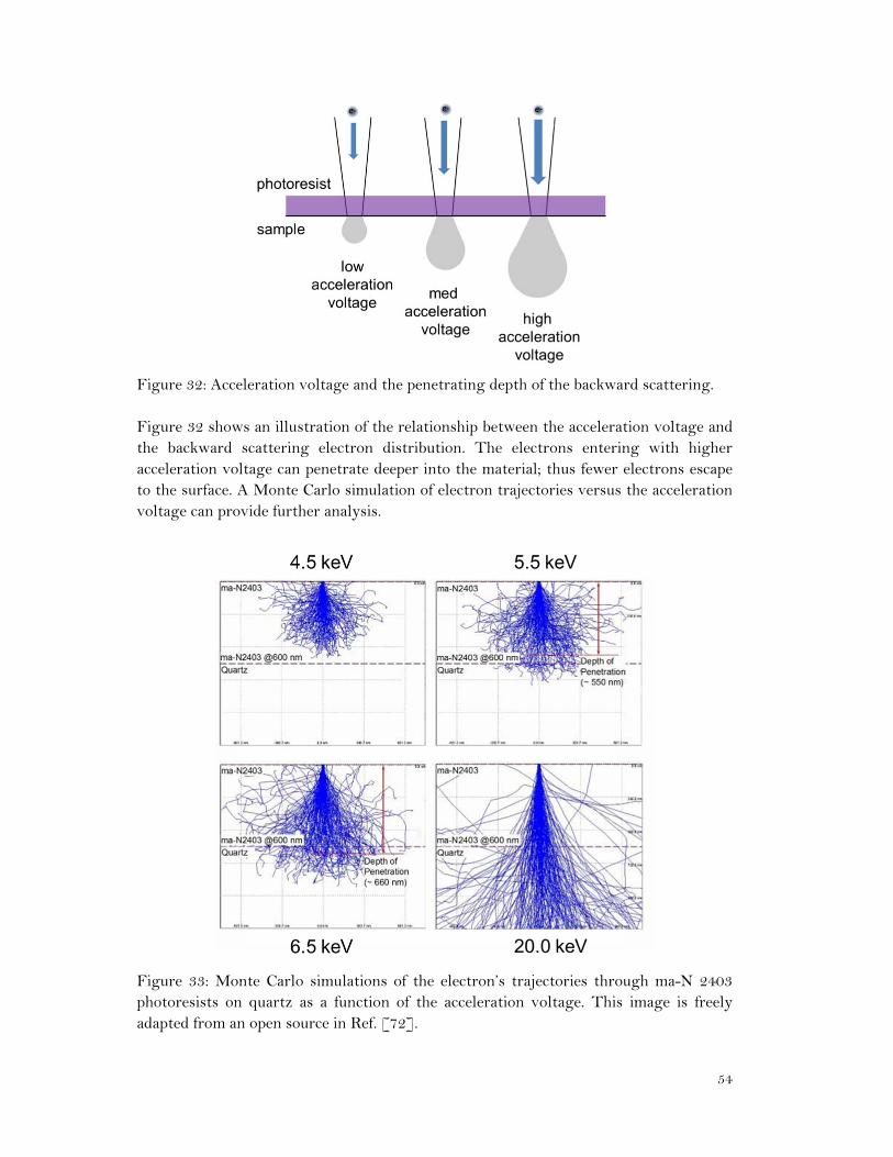
54
Figure 32: Acceleration voltage and the penetrating depth of the backward scattering. Figure 32 shows an illustration of the relationship between the acceleration voltage and the backward scattering electron distribution. The electrons entering with higher acceleration voltage can penetrate deeper into the material; thus fewer electrons escape to the surface. A Monte Carlo simulation of electron trajectories versus the acceleration voltage can provide further analysis.
Figure 33: Monte Carlo simulations of the electron’s trajectories through ma-N 2403 photoresists on quartz as a function of the acceleration voltage. This image is freely adapted from an open source in Ref. [72].
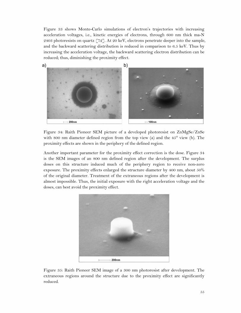
55
Figure 33 shows Monte-Carlo simulations of electron’s trajectories with increasing acceleration voltages, i.e., kinetic energies of electrons, through 600 nm thick ma-N 2403 photoresists on quartz [72]. At 20 keV, electrons penetrate deeper into the sample, and the backward scattering distribution is reduced in comparison to 6.5 keV. Thus by increasing the acceleration voltage, the backward scattering electron distribution can be reduced; thus, diminishing the proximity effect.
Figure 34: Raith Pioneer SEM picture of a developed photoresist on ZnMgSe/ZnSe with 800 nm diameter defined region from the top view (a) and the 45° view (b). The proximity effects are shown in the periphery of the defined region.
Another important parameter for the proximity effect correction is the dose. Figure 34 is the SEM images of an 800 nm defined region after the development. The surplus doses on this structure induced much of the periphery region to receive non-zero exposure. The proximity effects enlarged the structure diameter by 400 nm, about 50% of the original diameter. Treatment of the extraneous regions after the development is almost impossible. Thus, the initial exposure with the right acceleration voltage and the doses, can best avoid the proximity effect.
Figure 35: Raith Pioneer SEM image of a 300 nm photoresist after development. The extraneous regions around the structure due to the proximity effect are significantly reduced.
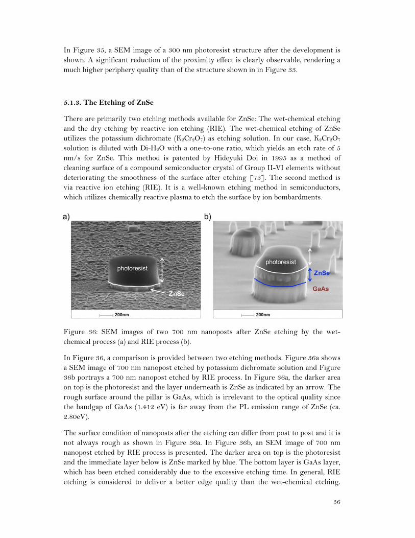
56
In Figure 35, a SEM image of a 300 nm photoresist structure after the development is shown. A significant reduction of the proximity effect is clearly observable, rendering a much higher periphery quality than of the structure shown in in Figure 33.
5.1.3. The Etching of ZnSe
There are primarily two etching methods available for ZnSe: The wet-chemical etching and the dry etching by reactive ion etching (RIE). The wet-chemical etching of ZnSe utilizes the potassium dichromate (K2Cr2O7) as etching solution. In our case, K2Cr2O7
solution is diluted with Di-H2O with a one-to-one ratio, which yields an etch rate of 5 nm/s for ZnSe. This method is patented by Hideyuki Doi in 1995 as a method of cleaning surface of a compound semiconductor crystal of Group II-VI elements without deteriorating the smoothness of the surface after etching [73]. The second method is via reactive ion etching (RIE). It is a well-known etching method in semiconductors, which utilizes chemically reactive plasma to etch the surface by ion bombardments.
Figure 36: SEM images of two 700 nm nanoposts after ZnSe etching by the wet-chemical process (a) and RIE process (b).
In Figure 36, a comparison is provided between two etching methods. Figure 36a shows a SEM image of 700 nm nanopost etched by potassium dichromate solution and Figure 36b portrays a 700 nm nanopost etched by RIE process. In Figure 36a, the darker area on top is the photoresist and the layer underneath is ZnSe as indicated by an arrow. The rough surface around the pillar is GaAs, which is irrelevant to the optical quality since the bandgap of GaAs (1.412 eV) is far away from the PL emission range of ZnSe (ca. 2.80eV).
The surface condition of nanoposts after the etching can differ from post to post and it is not always rough as shown in Figure 36a. In Figure 36b, an SEM image of 700 nm nanopost etched by RIE process is presented. The darker area on top is the photoresist and the immediate layer below is ZnSe marked by blue. The bottom layer is GaAs layer, which has been etched considerably due to the excessive etching time. In general, RIE etching is considered to deliver a better edge quality than the wet-chemical etching.
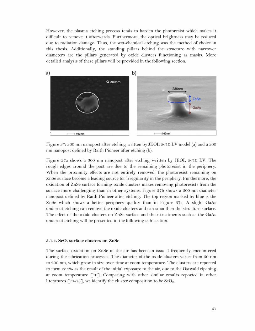
57
However, the plasma etching process tends to harden the photoresist which makes it difficult to remove it afterwards. Furthermore, the optical brightness may be reduced due to radiation damage. Thus, the wet-chemical etching was the method of choice in this thesis. Additionally, the standing pillars behind the structure with narrower diameters are the pillars generated by oxide clusters functioning as masks. More detailed analysis of these pillars will be provided in the following section.
Figure 37: 300 nm nanopost after etching written by JEOL 5610 LV model (a) and a 300 nm nanopost defined by Raith Pioneer after etching (b).
Figure 37a shows a 300 nm nanopost after etching written by JEOL 5610 LV. The rough edges around the post are due to the remaining photoresist in the periphery. When the proximity effects are not entirely removed, the photoresist remaining on ZnSe surface become a leading source for irregularity in the periphery. Furthermore, the oxidation of ZnSe surface forming oxide clusters makes removing photoresists from the surface more challenging than in other systems. Figure 37b shows a 300 nm diameter nanopost defined by Raith Pioneer after etching. The top region marked by blue is the ZnSe which shows a better periphery quality than in Figure 37a. A slight GaAs undercut etching can remove the oxide clusters and can smoothen the structure surface. The effect of the oxide clusters on ZnSe surface and their treatments such as the GaAs undercut etching will be presented in the following sub-section.
5.1.4. SeO2 surface clusters on ZnSe
The surface oxidation on ZnSe in the air has been an issue I frequently encountered during the fabrication processes. The diameter of the oxide clusters varies from 50 nm to 200 nm, which grow in size over time at room temperature. The clusters are reported to form ex situ as the result of the initial exposure to the air, due to the Ostwald ripening at room temperature [70]. Comparing with other similar results reported in other literatures [74-78], we identify the cluster composition to be SeO2.
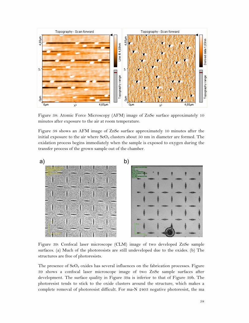
58
Figure 38: Atomic Force Microscopy (AFM) image of ZnSe surface approximately 10 minutes after exposure to the air at room temperature.
Figure 38 shows an AFM image of ZnSe surface approximately 10 minutes after the initial exposure to the air where SeO2 clusters about 50 nm in diameter are formed. The oxidation process begins immediately when the sample is exposed to oxygen during the transfer process of the grown sample out of the chamber.
Figure 39: Confocal laser microscope (CLM) image of two developed ZnSe sample surfaces. (a) Much of the photoresists are still undeveloped due to the oxides. (b) The structures are free of photoresists.
The presence of SeO2 oxides has several influences on the fabrication processes. Figure 39 shows a confocal laser microscope image of two ZnSe sample surfaces after development. The surface quality in Figure 39a is inferior to that of Figure 39b. The photoresist tends to stick to the oxide clusters around the structure, which makes a complete removal of photoresist difficult. For ma-N 2403 negative photoresist, the ma
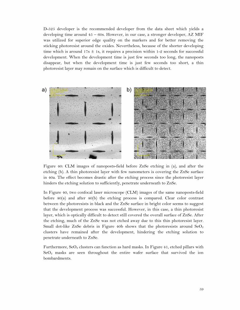
59
D-525 developer is the recommended developer from the data sheet which yields a developing time around 45 – 60s. However, in our case, a stronger developer, AZ MIF was utilized for superior edge quality on the markers and for better removing the sticking photoresist around the oxides. Nevertheless, because of the shorter developing time which is around 17s ± 1s, it requires a precision within 1-2 seconds for successful development. When the development time is just few seconds too long, the nanoposts disappear, but when the development time is just few seconds too short, a thin photoresist layer may remain on the surface which is difficult to detect.
Figure 40: CLM images of nanoposts-field before ZnSe etching in (a), and after the etching (b). A thin photoresist layer with few nanometers is covering the ZnSe surface in 40a. The effect becomes drastic after the etching process since the photoresist layer hinders the etching solution to sufficiently, penetrate underneath to ZnSe.
In Figure 40, two confocal laser microscope (CLM) images of the same nanoposts-field before 40(a) and after 40(b) the etching process is compared. Clear color contrast between the photoresists in black and the ZnSe surface in bright color seems to suggest that the development process was successful. However, in this case, a thin photoresist layer, which is optically difficult to detect still covered the overall surface of ZnSe. After the etching, much of the ZnSe was not etched away due to this thin photoresist layer. Small dot-like ZnSe debris in Figure 40b shows that the photoresists around SeO2 clusters have remained after the development, hindering the etching solution to penetrate underneath to ZnSe.
Furthermore, SeO2 clusters can function as hard masks. In Figure 41, etched pillars with SeO2 masks are seen throughout the entire wafer surface that survived the ion bombardments.
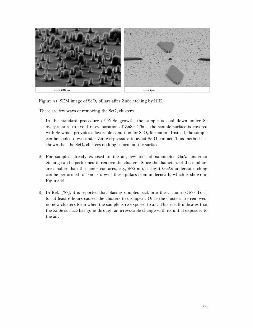
60
Figure 41: SEM image of SeO2 pillars after ZnSe etching by RIE.
There are few ways of removing the SeO2 clusters:
1) In the standard procedure of ZnSe growth, the sample is cool down under Se overpressure to avoid re-evaporation of ZnSe. Thus, the sample surface is covered with Se which provides a favorable condition for SeO2 formation. Instead, the sample can be cooled down under Zn overpressure to avoid Se-O contact. This method has shown that the SeO2 clusters no longer form on the surface.
2) For samples already exposed to the air, few tens of nanometer GaAs undercut
etching can be performed to remove the clusters. Since the diameters of these pillars are smaller than the nanostructures, e.g., 200 nm, a slight GaAs undercut etching can be performed to “knock down” these pillars from underneath, which is shown in Figure 42.
3) In Ref. [70], it is reported that placing samples back into the vacuum (<10-7 Torr)
for at least 6 hours caused the clusters to disappear. Once the clusters are removed, no new clusters form when the sample is re-exposed to air. This result indicates that the ZnSe surface has gone through an irrevocable change with its initial exposure to the air.
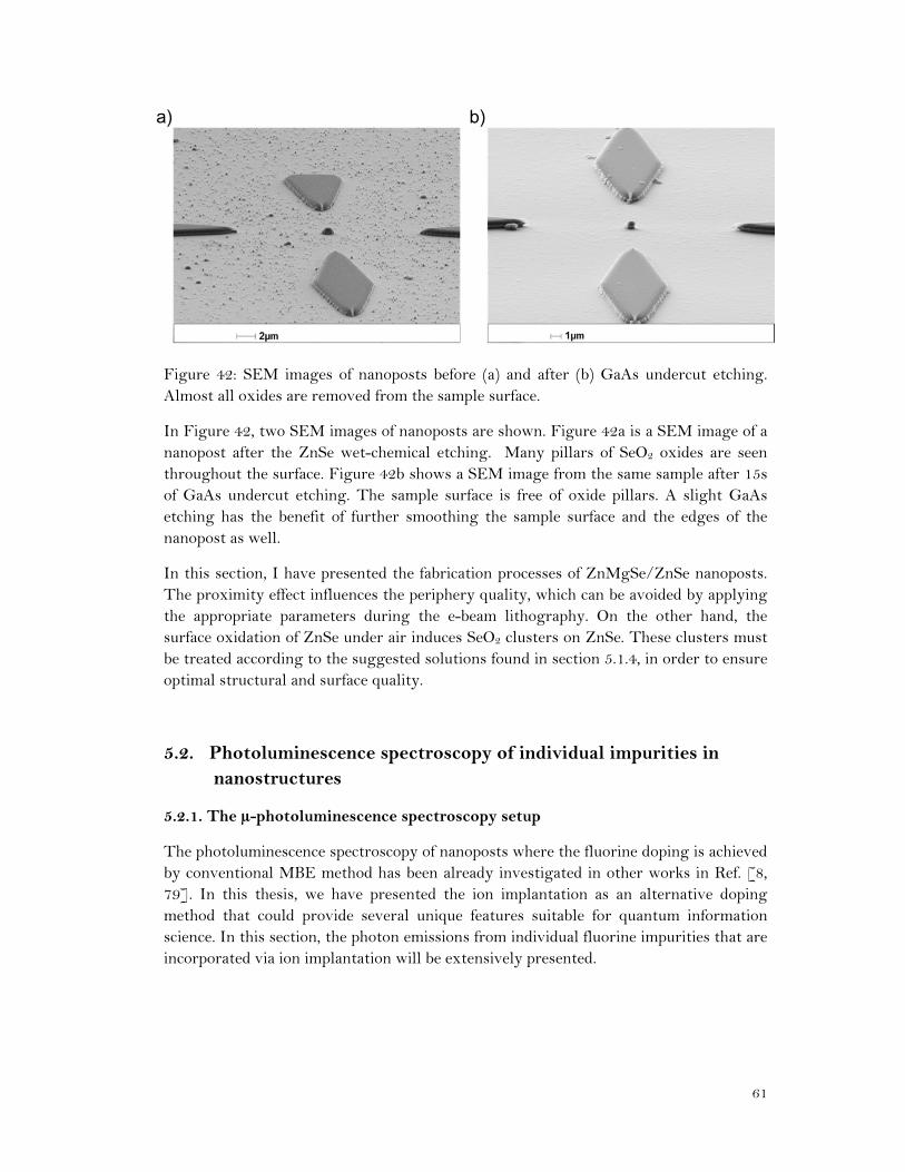
61
Figure 42: SEM images of nanoposts before (a) and after (b) GaAs undercut etching. Almost all oxides are removed from the sample surface.
In Figure 42, two SEM images of nanoposts are shown. Figure 42a is a SEM image of a nanopost after the ZnSe wet-chemical etching. Many pillars of SeO2 oxides are seen throughout the surface. Figure 42b shows a SEM image from the same sample after 15s of GaAs undercut etching. The sample surface is free of oxide pillars. A slight GaAs etching has the benefit of further smoothing the sample surface and the edges of the nanopost as well.
In this section, I have presented the fabrication processes of ZnMgSe/ZnSe nanoposts. The proximity effect influences the periphery quality, which can be avoided by applying the appropriate parameters during the e-beam lithography. On the other hand, the surface oxidation of ZnSe under air induces SeO2 clusters on ZnSe. These clusters must be treated according to the suggested solutions found in section 5.1.4, in order to ensure optimal structural and surface quality.
5.2. Photoluminescence spectroscopy of individual impurities in nanostructures
5.2.1. The μ-photoluminescence spectroscopy setup
The photoluminescence spectroscopy of nanoposts where the fluorine doping is achieved by conventional MBE method has been already investigated in other works in Ref. [8, 79]. In this thesis, we have presented the ion implantation as an alternative doping method that could provide several unique features suitable for quantum information science. In this section, the photon emissions from individual fluorine impurities that are incorporated via ion implantation will be extensively presented.
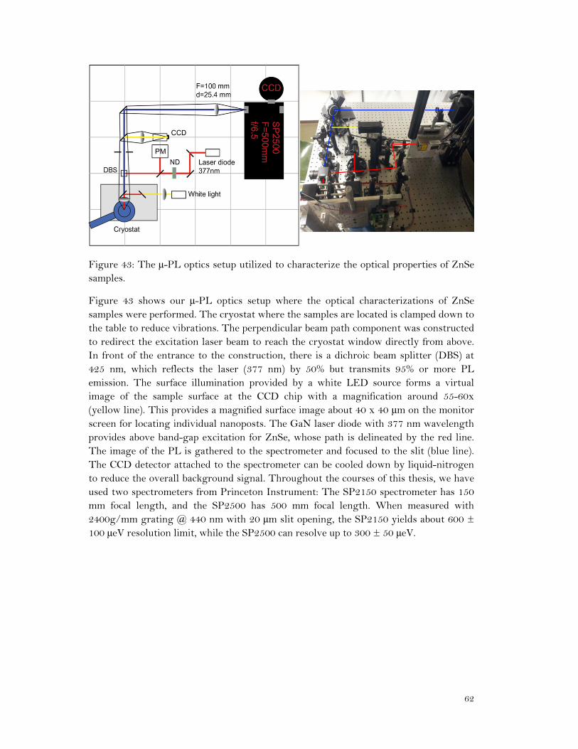
62
Figure 43: The μ-PL optics setup utilized to characterize the optical properties of ZnSe samples.
Figure 43 shows our μ-PL optics setup where the optical characterizations of ZnSe samples were performed. The cryostat where the samples are located is clamped down to the table to reduce vibrations. The perpendicular beam path component was constructed to redirect the excitation laser beam to reach the cryostat window directly from above. In front of the entrance to the construction, there is a dichroic beam splitter (DBS) at 425 nm, which reflects the laser (377 nm) by 50% but transmits 95% or more PL emission. The surface illumination provided by a white LED source forms a virtual image of the sample surface at the CCD chip with a magnification around 55-60x (yellow line). This provides a magnified surface image about 40 x 40 μm on the monitor screen for locating individual nanoposts. The GaN laser diode with 377 nm wavelength provides above band-gap excitation for ZnSe, whose path is delineated by the red line. The image of the PL is gathered to the spectrometer and focused to the slit (blue line). The CCD detector attached to the spectrometer can be cooled down by liquid-nitrogen to reduce the overall background signal. Throughout the courses of this thesis, we have used two spectrometers from Princeton Instrument: The SP2150 spectrometer has 150 mm focal length, and the SP2500 has 500 mm focal length. When measured with 2400g/mm grating @ 440 nm with 20 μm slit opening, the SP2150 yields about 600 ± 100 μeV resolution limit, while the SP2500 can resolve up to 300 ± 50 μeV.
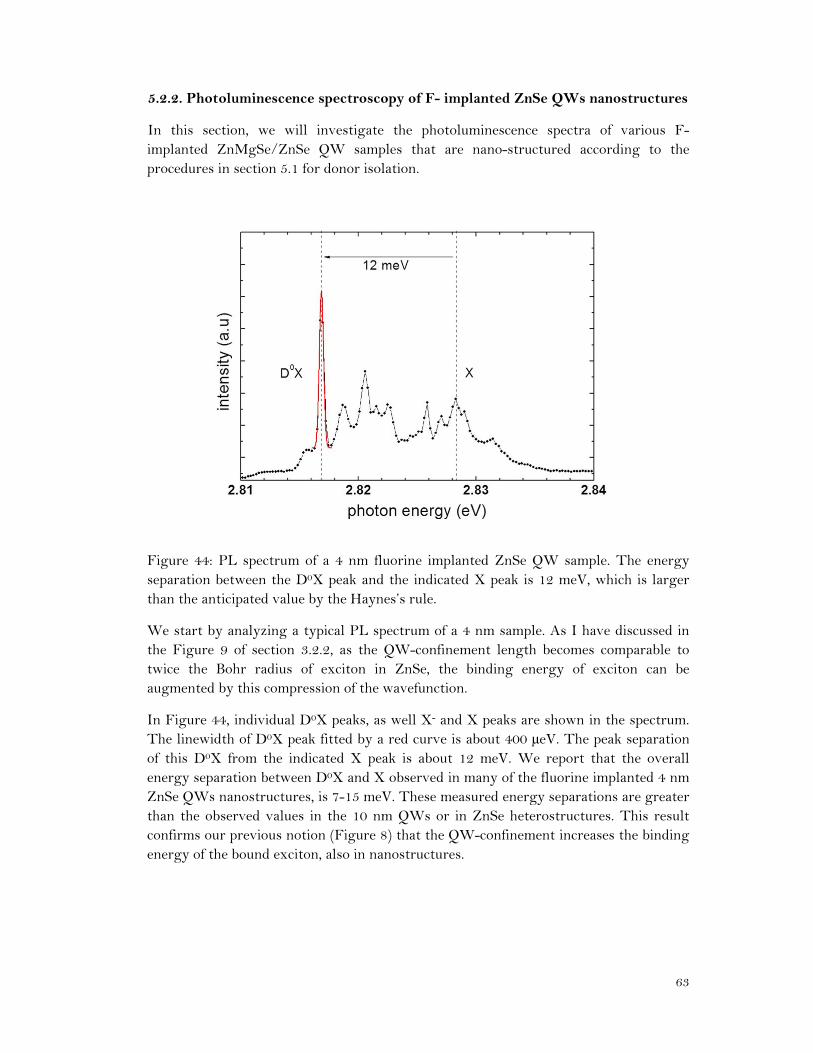
63
5.2.2. Photoluminescence spectroscopy of F- implanted ZnSe QWs nanostructures
In this section, we will investigate the photoluminescence spectra of various F-implanted ZnMgSe/ZnSe QW samples that are nano-structured according to the procedures in section 5.1 for donor isolation.
Figure 44: PL spectrum of a 4 nm fluorine implanted ZnSe QW sample. The energy separation between the D0X peak and the indicated X peak is 12 meV, which is larger than the anticipated value by the Haynes’s rule.
We start by analyzing a typical PL spectrum of a 4 nm sample. As I have discussed in the Figure 9 of section 3.2.2, as the QW-confinement length becomes comparable to twice the Bohr radius of exciton in ZnSe, the binding energy of exciton can be augmented by this compression of the wavefunction.
In Figure 44, individual D0X peaks, as well X- and X peaks are shown in the spectrum. The linewidth of D0X peak fitted by a red curve is about 400 μeV. The peak separation of this D0X from the indicated X peak is about 12 meV. We report that the overall energy separation between D0X and X observed in many of the fluorine implanted 4 nm ZnSe QWs nanostructures, is 7-15 meV. These measured energy separations are greater than the observed values in the 10 nm QWs or in ZnSe heterostructures. This result confirms our previous notion (Figure 8) that the QW-confinement increases the binding energy of the bound exciton, also in nanostructures.
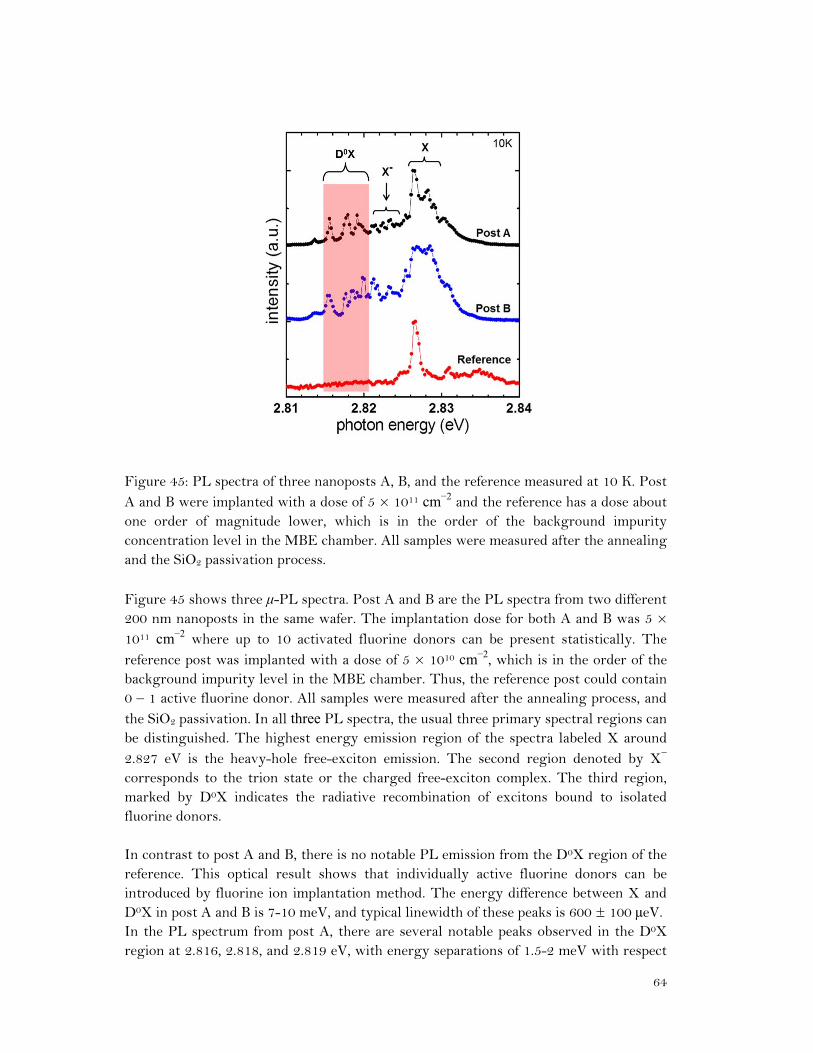
64
Figure 45: PL spectra of three nanoposts A, B, and the reference measured at 10 K. Post A and B were implanted with a dose of 5 × 1011 cm−2 and the reference has a dose about one order of magnitude lower, which is in the order of the background impurity concentration level in the MBE chamber. All samples were measured after the annealing and the SiO2 passivation process. Figure 45 shows three μ-PL spectra. Post A and B are the PL spectra from two different 200 nm nanoposts in the same wafer. The implantation dose for both A and B was 5 × 1011 cm−2 where up to 10 activated fluorine donors can be present statistically. The reference post was implanted with a dose of 5 × 1010 cm−2, which is in the order of the background impurity level in the MBE chamber. Thus, the reference post could contain 0 – 1 active fluorine donor. All samples were measured after the annealing process, and the SiO2 passivation. In all three PL spectra, the usual three primary spectral regions can be distinguished. The highest energy emission region of the spectra labeled X around 2.827 eV is the heavy-hole free-exciton emission. The second region denoted by X− corresponds to the trion state or the charged free-exciton complex. The third region, marked by D0X indicates the radiative recombination of excitons bound to isolated fluorine donors. In contrast to post A and B, there is no notable PL emission from the D0X region of the reference. This optical result shows that individually active fluorine donors can be introduced by fluorine ion implantation method. The energy difference between X and D0X in post A and B is 7-10 meV, and typical linewidth of these peaks is 600 ± 100 μeV. In the PL spectrum from post A, there are several notable peaks observed in the D0X region at 2.816, 2.818, and 2.819 eV, with energy separations of 1.5-2 meV with respect
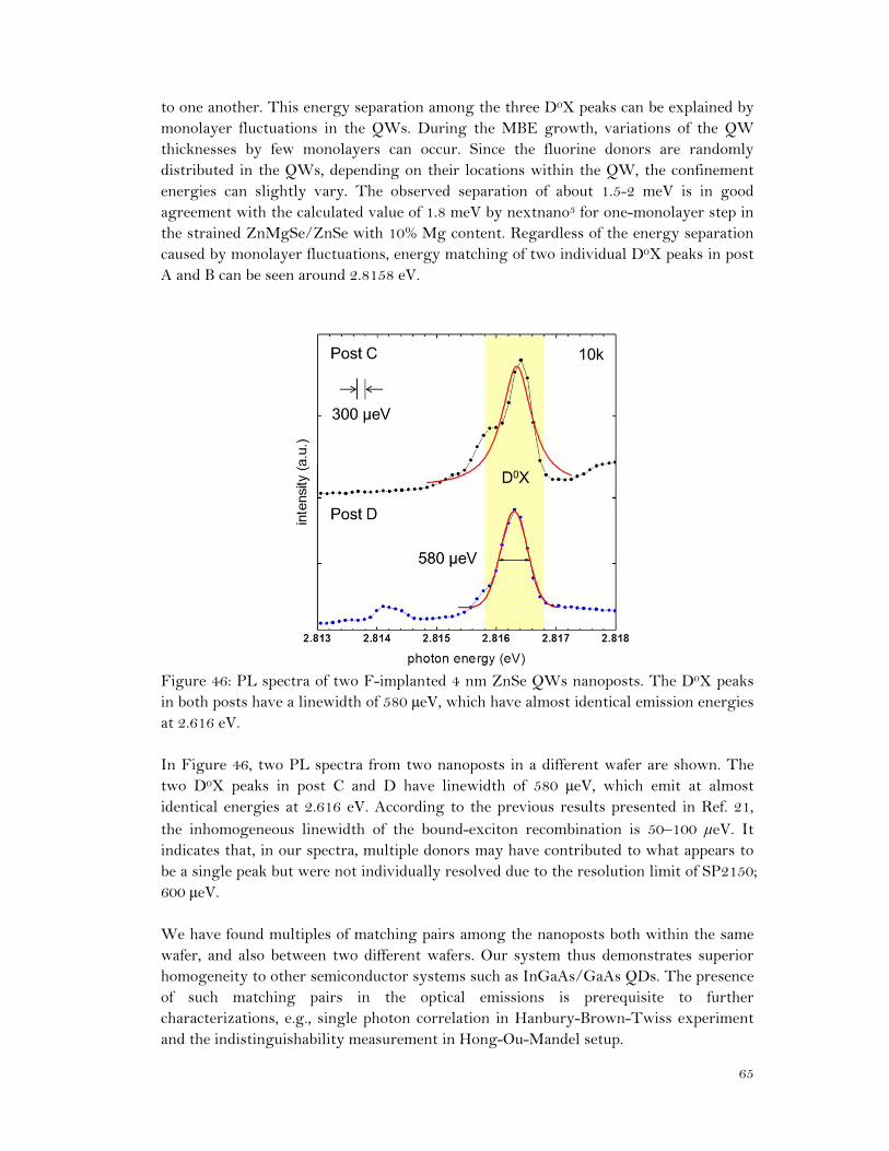
65
to one another. This energy separation among the three D0X peaks can be explained by monolayer fluctuations in the QWs. During the MBE growth, variations of the QW thicknesses by few monolayers can occur. Since the fluorine donors are randomly distributed in the QWs, depending on their locations within the QW, the confinement energies can slightly vary. The observed separation of about 1.5-2 meV is in good agreement with the calculated value of 1.8 meV by nextnano3 for one-monolayer step in the strained ZnMgSe/ZnSe with 10% Mg content. Regardless of the energy separation caused by monolayer fluctuations, energy matching of two individual D0X peaks in post A and B can be seen around 2.8158 eV.
Figure 46: PL spectra of two F-implanted 4 nm ZnSe QWs nanoposts. The D0X peaks in both posts have a linewidth of 580 μeV, which have almost identical emission energies at 2.616 eV. In Figure 46, two PL spectra from two nanoposts in a different wafer are shown. The two D0X peaks in post C and D have linewidth of 580 μeV, which emit at almost identical energies at 2.616 eV. According to the previous results presented in Ref. 21, the inhomogeneous linewidth of the bound-exciton recombination is 50–100 μeV. It indicates that, in our spectra, multiple donors may have contributed to what appears to be a single peak but were not individually resolved due to the resolution limit of SP2150; 600 μeV. We have found multiples of matching pairs among the nanoposts both within the same wafer, and also between two different wafers. Our system thus demonstrates superior homogeneity to other semiconductor systems such as InGaAs/GaAs QDs. The presence of such matching pairs in the optical emissions is prerequisite to further characterizations, e.g., single photon correlation in Hanbury-Brown-Twiss experiment and the indistinguishability measurement in Hong-Ou-Mandel setup.
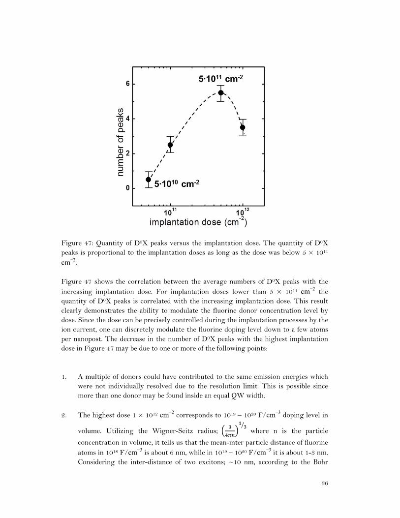
66
Figure 47: Quantity of D0X peaks versus the implantation dose. The quantity of D0X peaks is proportional to the implantation doses as long as the dose was below 5 × 1011 cm−2. Figure 47 shows the correlation between the average numbers of D0X peaks with the increasing implantation dose. For implantation doses lower than 5 × 1011 cm−2 the quantity of D0X peaks is correlated with the increasing implantation dose. This result clearly demonstrates the ability to modulate the fluorine donor concentration level by dose. Since the dose can be precisely controlled during the implantation processes by the ion current, one can discretely modulate the fluorine doping level down to a few atoms per nanopost. The decrease in the number of D0X peaks with the highest implantation dose in Figure 47 may be due to one or more of the following points: 1. A multiple of donors could have contributed to the same emission energies which
were not individually resolved due to the resolution limit. This is possible since more than one donor may be found inside an equal QW width.
2. The highest dose 1 × 1012 cm−2 corresponds to 1019 – 1020 F/cm−3 doping level in
volume. Utilizing the Wigner-Seitz radius; where n is the particle
concentration in volume, it tells us that the mean-inter particle distance of fluorine atoms in 1018 F/cm−3 is about 6 nm, while in 1019 – 1020 F/cm−3 it is about 1-3 nm. Considering the inter-distance of two excitons; ~10 nm, according to the Bohr
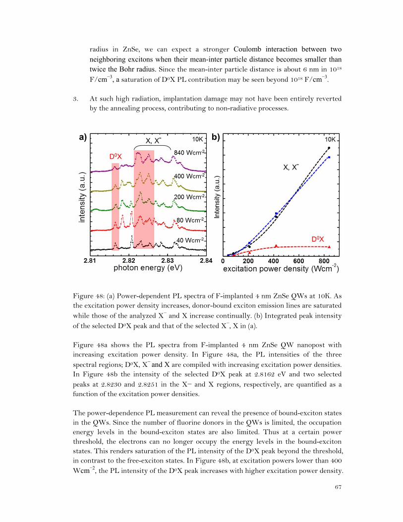
67
radius in ZnSe, we can expect a stronger Coulomb interaction between two neighboring excitons when their mean-inter particle distance becomes smaller than twice the Bohr radius. Since the mean-inter particle distance is about 6 nm in 1018 F/cm−3, a saturation of D0X PL contribution may be seen beyond 1018 F/cm−3.
3. At such high radiation, implantation damage may not have been entirely reverted by the annealing process, contributing to non-radiative processes.
Figure 48: (a) Power-dependent PL spectra of F-implanted 4 nm ZnSe QWs at 10K. As the excitation power density increases, donor-bound exciton emission lines are saturated while those of the analyzed X− and X increase continually. (b) Integrated peak intensity of the selected D0X peak and that of the selected X−, X in (a). Figure 48a shows the PL spectra from F-implanted 4 nm ZnSe QW nanopost with increasing excitation power density. In Figure 48a, the PL intensities of the three spectral regions; D0X, X− and X are compiled with increasing excitation power densities. In Figure 48b the intensity of the selected D0X peak at 2.8162 eV and two selected peaks at 2.8230 and 2.8251 in the X− and X regions, respectively, are quantified as a function of the excitation power densities. The power-dependence PL measurement can reveal the presence of bound-exciton states in the QWs. Since the number of fluorine donors in the QWs is limited, the occupation energy levels in the bound-exciton states are also limited. Thus at a certain power threshold, the electrons can no longer occupy the energy levels in the bound-exciton states. This renders saturation of the PL intensity of the D0X peak beyond the threshold, in contrast to the free-exciton states. In Figure 48b, at excitation powers lower than 400 Wcm−2, the PL intensity of the D0X peak increases with higher excitation power density.
68
However, at excitation powers higher than 400 Wcm−2 the intensity of the indicated D0X peak is saturated, while that of the two peaks in the X− and X regions show a superlinear increase for higher excitation power. This result clearly indicates the presence of bound-exciton states in the QWs due to the incorporated fluorine donors via ion implantation.
5.3. Summary In this chapter, we have introduced fabrication processes of ZnMgSe/ZnSe nanoposts as means of isolating individual fluorine impurities. 100 – 700 nm diameter nanoposts were defined by electron beam lithography with optimized acceleration voltage and the dose to minimize the proximity effect. The ZnSe surface with Selenium layer on top is vulnerable to SeO2 cluster formation, and treatment of these clusters is essential for optimal structural and surface quality. Furthermore, the photoluminescence spectroscopy of F-implanted ZnSe QWs nanoposts was investigated: the number of D0X peaks in the PL spectrum tends to increase with higher implantation dose until 5 × 1011 cm−2. The D0X peaks saturate in contrast to X, X- peaks that show superlinear augmentation with increasing excitation power. These experimental evidences demonstrate successful ion implantation of fluorine impurities as active donors in the ZnMgSe/ZnSe QWs nanoposts applicable for quantum information science technology.

69
Chapter 6
Bound electron spins under external magnetic field
In this chapter, we will investigate the behavior of bound electron spins in fluorine donors when an external magnetic field is applied. The presence of optically controllable spin qubit states under the Zeeman splitting were reported from ZnSe:F QWs nanostructured samples doped via MBE in Ref. [8, 79]. Here, we verify the presence of equivalently valid spin qubit states from ZnSe:F QWs nanostructured samples that are implanted with fluorine impurities as donors. Moreover, the selection rules governing the allowed optical transitions in our system will be discussed and supported by experimental evidences demonstrating the fully-connected nature of these transitions in our system.
6.1. Non-degenerate donor states in ZnSe:F under Zeeman splitting
Before going into detailed analysis on the experimental results, I would like to provide a brief review on the quantum states of our system described in this chapter. Recall that the four fundamental quantum numbers are: the principal quantum number n (energy level), azimuthal quantum number l (orbital quantum number; s, p, d, etc.), magnetic quantum number ml (projection of the orbital angular momentum along an axis), and the spin projection quantum number ms.
It is known in semiconductor physics that the electrons in the conduction band have s-like orbital wavefunction while holes have p-like orbital wavefunction. Since the spin-orbit interaction couples the orbital angular momentum to the spin momentum the
total angular momentum of a particle can be written as:
= + (6.1)
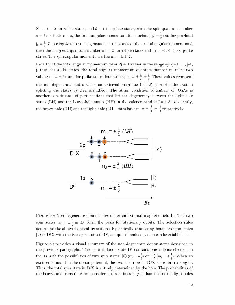
70
Since l = 0 for s-like states, and l = 1 for p-like states, with the spin quantum number
s = ½ in both cases, the total angular momentum for s-orbital, js = and for p-orbital
jp = . Choosing lz to be the eigenstates of the z-axis of the orbital angular momentum ,
then the magnetic quantum number ml = 0 for s-like states and ml = -1, 0, 1 for p-like states. The spin angular momentum has ms = ± 1/2.
Recall that the total angular momentum takes 2j + 1 values in the range –j, -j+1, …, j-1, j, thus, for s-like states, the total angular momentum quantum number mj takes two
values; mj = ± ½, and for p-like states four values; mj = ± , ± . These values represent
the non-degenerate states when an external magnetic field perturbs the system splitting the states by Zeeman Effect. The strain condition of ZnSe:F on GaAs is another constituents of perturbations that lift the degeneracy between the light-hole states (LH) and the heavy-hole states (HH) in the valence band at Γ=0. Subsequently,
the heavy-hole (HH) and the light-hole (LH) states have mj = ± , ± respectively.
Figure 49: Non-degenerate donor states under an external magnetic field Bz. The two
spin states mj = ± in D0 form the basis for stationary qubits. The selection rules
determine the allowed optical transitions. By optically connecting bound exciton states | in D0X with the two spin states in D0, an optical lambda system can be established.
Figure 49 provides a visual summary of the non-degenerate donor states described in the previous paragraphs. The neutral donor state D0 contains one valence electron in
the 1s with the possibilities of two spin states; |0 (mj = - ) or |1 (mj = + ). When an
exciton is bound in the donor potential, the two electrons in D0X state form a singlet. Thus, the total spin state in D0X is entirely determined by the hole. The probabilities of the heavy-hole transitions are considered three times larger than that of the light-holes
71
[80]; thus we only consider the heavy-hole transitions in our optical analysis. The two spin states; |0 and |1 , in D0 form the basis for stationary qubits where the spin information of an electron can be stored. By optically connecting bound exciton states | in D0X with the two spin states in D0, an optical lambda system can be established. The optical transitions particularly follow the conservation of the angular momentum of the photons which allow only ΔmJ = ± 1 transitions from D0X to D0. This leads to the
selection rules to govern the allowed transitions in a given orientation. The two orthogonal magnetic orientations; Faraday and Voigt, play a crucial role for determining the allowed optical transitions, which will be derived in section 6.2.
6.1.1. g-factor of electrons and holes in ZnSe
A g-factor is a proportionality constant which characterizes the magnetic moment with the appropriate angular momentum quantum number and the Bohr magneton under a magnetic field. It essentially describes the Zeeman splitting factor of non-degenerate particle states under a given magnetic field strength B. Consider a free electron which has a magnetic moment:
(6.2)
where is the Landé g-factor of a free electron, is the Bohr magneton and is
the electron spin operator with , , .
When an electron is in a magnetic field , the magnetic moment of the electron and the magnetic field interacts to yield an energy E:
∙ (6.3)
where is the electron spin projection quantum number.
Thus, the energy separation of the two spin states under magnetic field strength B is:
∆ (6.4)
In the ZnSe semiconductor, electrons are not free but under the periodic potential of the ZnSe lattice. Thus, the application of the equation (5.4) can be made by replacing the Landé g-factor of a free electron by effective g-factors; ge for the electron in D0, and ghh for the heavy-hole in D0X state. This is an analogous substituting process of m0 by the effective mass of electron me* in the crystal lattice. The electrons and holes have different g-factors [81], and their g-factors are also dependent on temperature and doping concentration [82]. Through measuring the energy separation between the two spin states selectively by polarization, the g-factors of the electron and the hole can be obtained.
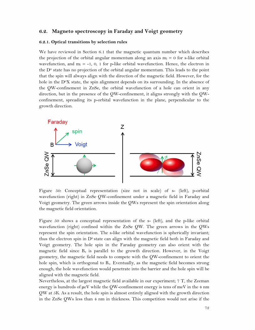
72
6.2. Magneto spectroscopy in Faraday and Voigt geometry
6.2.1. Optical transitions by selection rules
We have reviewed in Section 6.1 that the magnetic quantum number which describes the projection of the orbital angular momentum along an axis ml = 0 for s-like orbital wavefunction, and ml = -1, 0, 1 for p-like orbital wavefunction. Hence, the electron in the D0 state has no projection of the orbital angular momentum. This leads to the point that the spin will always align with the direction of the magnetic field. However, for the hole in the D0X state, the spin alignment depends on its surrounding. In the absence of the QW-confinement in ZnSe, the orbital wavefunction of a hole can orient in any direction, but in the presence of the QW-confinement, it aligns strongly with the QW-confinement, spreading its p-orbital wavefunction in the plane, perpendicular to the growth direction.
Figure 50: Conceptual representation (size not in scale) of s- (left), p-orbital wavefunction (right) in ZnSe QW-confinement under a magnetic field in Faraday and Voigt geometry. The green arrows inside the QWs represent the spin orientation along the magnetic field orientation. Figure 50 shows a conceptual representation of the s- (left), and the p-like orbital wavefunction (right) confined within the ZnSe QW. The green arrows in the QWs represent the spin orientation. The s-like orbital wavefunction is spherically invariant; thus the electron spin in D0 state can align with the magnetic field both in Faraday and Voigt geometry. The hole spin in the Faraday geometry can also orient with the magnetic field since Bz is parallel to the growth direction. However, in the Voigt geometry, the magnetic field needs to compete with the QW-confinement to orient the hole spin, which is orthogonal to Bx. Eventually, as the magnetic field becomes strong enough, the hole wavefunction would penetrate into the barrier and the hole spin will be aligned with the magnetic field. Nevertheless, at the largest magnetic field available in our experiment; 7 T, the Zeeman energy is hundreds of μeV while the QW-confinement energy is tens of meV in the 4 nm QW at 5K. As a result, the hole spin is almost entirely aligned with the growth direction in the ZnSe QWs less than 4 nm in thickness. This competition would not arise if the
73
QW-width is sufficiently larger than twice the Bohr radius in ZnSe, but it becomes observable when the QW-width is 2-4 nm. The g-factor of the hole in Voigt, often takes smaller value than that of the electron in Voigt geometry. This could be due to the fact that the magnetic field contribution in the perpendicular direction to the growth direction is small, and/or the spin-spin coupling and the spin-orbit coupling may cancel out one another in Voigt geometry. Furthermore, the competition between the magnetic field and the growth direction attempting to orient the spin, causes a mixture of the hole spin states in the D0X, allowing additional optical transitions. These superposition states have the frequency of the phase oscillations, and can be described for our system, using the Larmor frequency:
∗
where g* is the effective g-factor of the electron and hole in our system, instead of the free electron g-factor. Recall that mJ = ± 3/2 for the heavy-holes, which define the two spin states in the D0X
as | and| , and mJ = ± 1/2 defining the spin states of electron in D0 as | and
| . In the Faraday geometry, the magnetic field as well as the growth direction aligns
the spin orientation to . Since the conservation of the angular momentum of the photons only allows ΔmJ = ± 1 between D0X → D0, two optical transitions are
permitted in the Faraday geometry: | → | or | → | .
Here we empirically derive the optical transitions in Faraday geometry by utilizing the
Fermi’s golden rule where the time-independent is abruptly introduced:
→ ∝ | Ψ Ψ | ∙
(6.5)
where the perturbed Hamiltonian = ∙ , is the electric dipole operator for
spontaneous emission in the electric dipole approximation. The two spin states |
and | in D0 can be defined as: (6.6)
|Ψ ,12
| | | ↓
|Ψ ,12
| | | ↑
where and represent the envelope function and the Bloch wavefunction of delocalized electron in the conduction band which spans through ZnSe crystal. These expressions account for the envelope function approximation which postulates that the wavefunction can be written in terms of a slowly varying envelope function that modulates the Bloch function. Furthermore, the two electrons in D0X state form a singlet:
| |√
| ↑↓ | ↓↑ (6.7)
74
Thus, the spin in D0X state is determined by the hole.
In Faraday geometry, the two hole states | and| are defined: (6.8)
|Ψ ,32
| | | ↓
|Ψ ,32
| | | ↑
where represents the Bloch function of a heavy-hole. Applying the Fermi’s golden rule, four possible combinations are given: (6.9)
,→
,∝ Ψ ,
12
∙ Ψ ,32
,→ ∝ Ψ ,
12
∙ Ψ ,32
,→
,∝ Ψ ,
12
∙ Ψ ,32
,→
, ∝ Ψ , ∙ Ψ ,
By substituting the appropriate envelope functions and the Bloch wavefunctions, (6.10)
,
→,∝ ↓ | | | ∙ | | | ↓
,
→ ∝ ↑ | | | ∙ | | | ↓
,
→,
∝ ↑ | | | ∙ | | | ↑
,
→,
∝ ↓ | | | ∙ | | | ↑
The Bloch functions in both D0 and D0X are nearly identical. Given that the variation of
the envelop function and the is small in the dimension of ZnSe lattice parameter; ~0.56 nm < Bohr radius; 5 nm, (6.10) can be simplified: (6.11) (1) (2) (3)
,→
,∝ ↓ | ↓ ∙ | |
,→ ∝ | ↑ | ↓ | ∙ | |
,→
,∝ | ↑ | ↑ | ∙ | |
,→
,∝ | ↓ | ↑ | ∙ | |
Recall that the two qubits are defined as orthonormal in the same orientation, and thus satisfy the following inner product properties: (6.12)
↓ | ↓ ↑ | ↑ 1, ↓ | ↑ ↑ | ↓ 0.
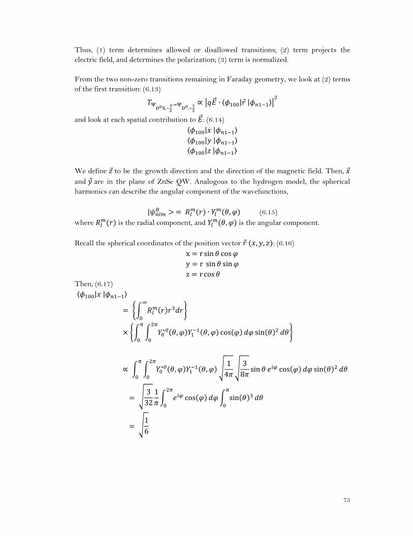
75
Thus, (1) term determines allowed or disallowed transitions; (2) term projects the electric field, and determines the polarization; (3) term is normalized. From the two non-zero transitions remaining in Faraday geometry, we look at (2) terms of the first transition: (6.13)
,→
,∝ ∙ | |
and look at each spatial contribution to : (6.14) | | | | | |
We define to be the growth direction and the direction of the magnetic field. Then, and are in the plane of ZnSe QW. Analogous to the hydrogen model, the spherical harmonics can describe the angular component of the wavefunctions,
| ∙ , (6.15)
where is the radial component, and , is the angular component. Recall the spherical coordinates of the position vector , , : (6.16)
x r sin cos y r sin sin z r cos
Then, (6.17) | |
∗ , , cos sin
∝ ∗ , ,14
38
sin cos sin
332
1cos sin
16
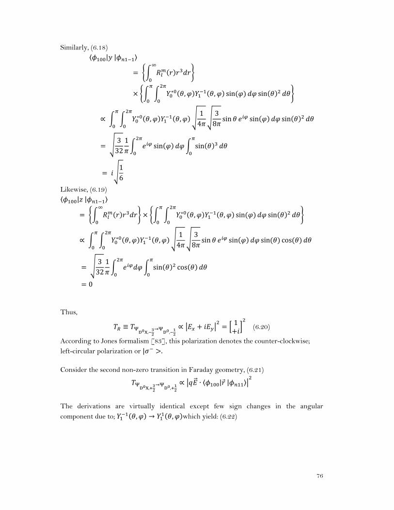
76
Similarly, (6.18) | |
∗ , , sin sin
∝ ∗ , ,14
38
sin sin sin
332
1sin sin
16
Likewise, (6.19) | |
∗ , , sin sin
∝ ∗ , ,14
38
sin sin sin cos
332
1sin cos
0 Thus,
≡,
→,
∝ 1 (6.20)
According to Jones formalism [83], this polarization denotes the counter-clockwise; left-circular polarization or | . Consider the second non-zero transition in Faraday geometry, (6.21)
,→
,∝ ∙ | |
The derivations are virtually identical except few sign changes in the angular
component due to; , → , which yield: (6.22)
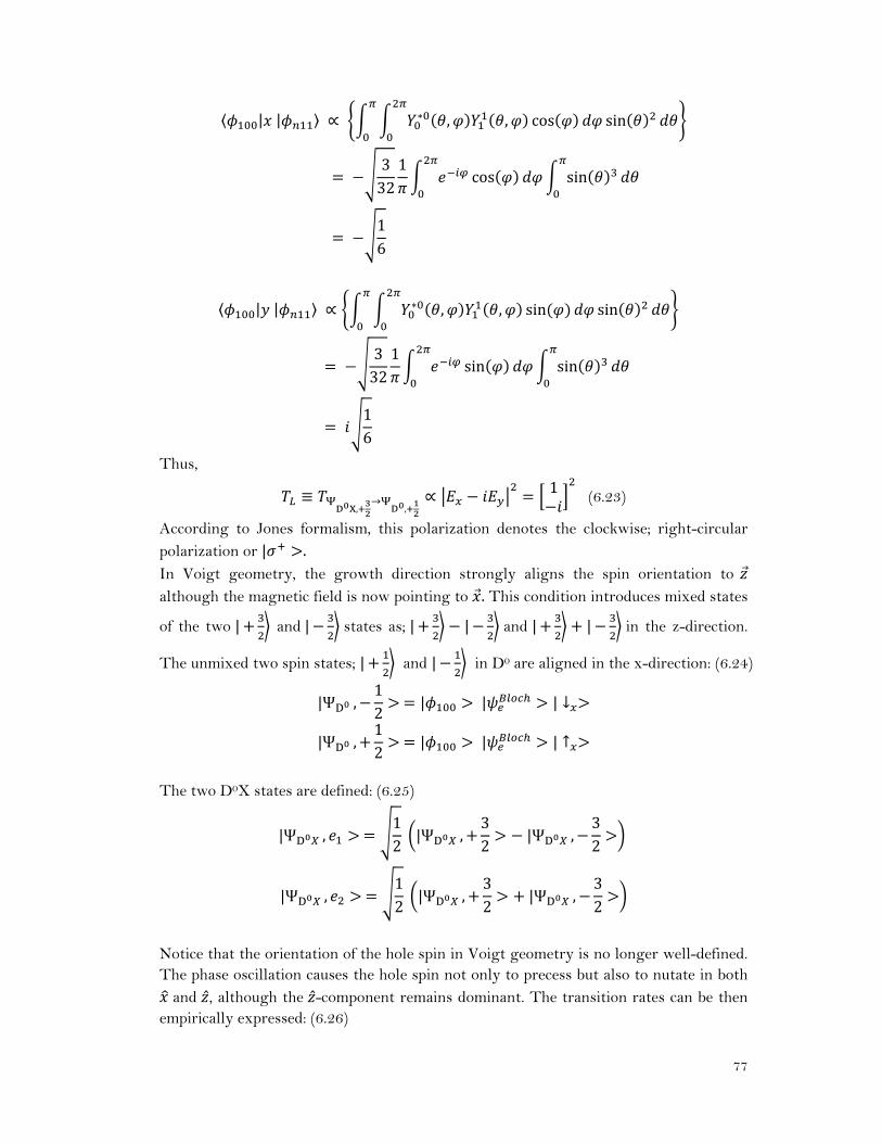
77
| | ∝ ∗ , , cos sin
332
1cos sin
16
| | ∝ ∗ , , sin sin
332
1sin sin
16
Thus,
≡,
→,
∝ 1 (6.23)
According to Jones formalism, this polarization denotes the clockwise; right-circular polarization or | . In Voigt geometry, the growth direction strongly aligns the spin orientation to although the magnetic field is now pointing to . This condition introduces mixed states
of the two | and| states as; | | and | | in the z-direction.
The unmixed two spin states; | and | in D0 are aligned in the x-direction: (6.24)
|Ψ ,12
| | | ↓
|Ψ ,12
| | | ↑
The two D0X states are defined: (6.25)
|Ψ , 12 |Ψ ,
32
|Ψ ,32
|Ψ , 12 |Ψ ,
32
|Ψ ,32
Notice that the orientation of the hole spin in Voigt geometry is no longer well-defined. The phase oscillation causes the hole spin not only to precess but also to nutate in both
and , although the -component remains dominant. The transition rates can be then empirically expressed: (6.26)
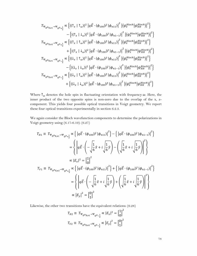
78
, → ∝ | ↑ | ↑ | ∙ | |
| ↑ | ↓ | ∙ | |
, → ∝ | ↑ | ↑ | ∙ | |
| ↑ | ↓ | ∙ | |
, → ∝ | ↓ | ↑ | ∙ | |
| ↓ | ↓ | ∙ | |
, → ∝ | ↓ | ↑ | ∙ | |
| ↓ | ↓ | ∙ | |
Where ↑ denotes the hole spin in fluctuating orientation with frequency . Here, the inner product of the two opposite spins is non-zero due to the overlap of the x, z-component. This yields four possible optical transitions in Voigt geometry. We report these four optical transitions experimentally in section 6.2.3. We again consider the Bloch wavefunction components to determine the polarizations in Voigt geometry using (6.17-6.19): (6.27)
≡ , → ∝ ∙ | | ∙ | |
∙16
16
16
16
∝ | | 10
≡ , → ∝ ∙ | | ∙ | |
∙16
16
16
16
∝ 01
Likewise, the other two transitions have the equivalent relations: (6.28)
≡ , → ∝ | | 1
0
≡ , → ∝ 0
1
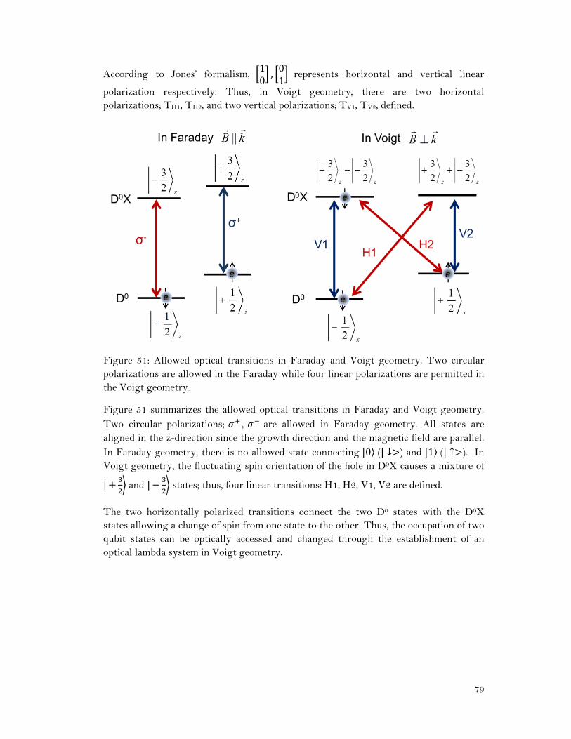
79
According to Jones’ formalism, 10, 01
represents horizontal and vertical linear
polarization respectively. Thus, in Voigt geometry, there are two horizontal polarizations; TH1, TH2, and two vertical polarizations; TV1, TV2, defined.
Figure 51: Allowed optical transitions in Faraday and Voigt geometry. Two circular polarizations are allowed in the Faraday while four linear polarizations are permitted in the Voigt geometry.
Figure 51 summarizes the allowed optical transitions in Faraday and Voigt geometry. Two circular polarizations; , are allowed in Faraday geometry. All states are aligned in the z-direction since the growth direction and the magnetic field are parallel. In Faraday geometry, there is no allowed state connecting |0 (| ↓ ) and |1 (| ↑ ). In Voigt geometry, the fluctuating spin orientation of the hole in D0X causes a mixture of
| and | states; thus, four linear transitions: H1, H2, V1, V2 are defined.
The two horizontally polarized transitions connect the two D0 states with the D0X states allowing a change of spin from one state to the other. Thus, the occupation of two qubit states can be optically accessed and changed through the establishment of an optical lambda system in Voigt geometry.
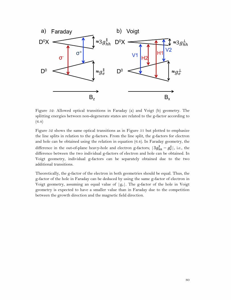
80
Figure 52: Allowed optical transitions in Faraday (a) and Voigt (b) geometry. The splitting energies between non-degenerate states are related to the g-factor according to (6.4)
Figure 52 shows the same optical transitions as in Figure 51 but plotted to emphasize the line splits in relation to the g-factors. From the line split, the g-factors for electron and hole can be obtained using the relation in equation (6.4). In Faraday geometry, the
difference in the out-of-plane heavy-hole and electron g-factors; |3 ∥ ∥|, i.e., the difference between the two individual g-factors of electron and hole can be obtained. In Voigt geometry, individual g-factors can be separately obtained due to the two additional transitions.
Theoretically, the g-factor of the electron in both geometries should be equal. Thus, the g-factor of the hole in Faraday can be deduced by using the same g-factor of electron in Voigt geometry, assuming an equal value of |ge|. The g-factor of the hole in Voigt geometry is expected to have a smaller value than in Faraday due to the competition between the growth direction and the magnetic field direction.
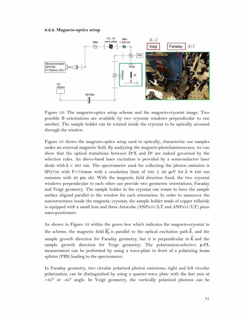
81
6.2.2. Magneto-optics setup
Figure 53: The magneto-optics setup scheme and the magneto-cryostat image. Two possible B orientations are available by two cryostat windows perpendicular to one another. The sample holder can be rotated inside the cryostat to be optically accessed through the window. Figure 53 shows the magneto-optics setup used to optically, characterize our samples under an external magnetic field. By analyzing the magneto-photoluminescence, we can show that the optical transitions between D0X and D0 are indeed governed by the selection rules. An above-band laser excitation is provided by a semiconductor laser diode with λ = 405 nm. The spectrometer used for collecting the photon emission is SP2750 with F=750mm with a resolution limit of 100 ± 20 μeV for λ 440 nm emission with 20 μm slit. With the magnetic field direction fixed, the two cryostat windows perpendicular to each other can provide two geometric orientations; Faraday and Voigt geometry. The sample holder in the cryostat can rotate to have the sample surface aligned parallel to the window for each orientation. In order to maneuver the nanostructures inside the magnetic cryostat, the sample holder made of copper telluride is equipped with a small lens and three Attocube (ANPx51/LT and ANPz51/LT) piezo nano-positioners. As shown in Figure 53 within the green box which indicates the magneto-cryostat in
the scheme, the magnetic field is parallel to the optical excitation path , and the
sample growth direction for Faraday geometry, but it is perpendicular to and the sample growth direction for Voigt geometry. The polarization-selective μ-PL measurement can be performed by using a wave-plate in front of a polarizing beam splitter (PBS) leading to the spectrometer. In Faraday geometry, two circular polarized photon emissions; right and left circular polarization, can be distinguished by using a quarter-wave plate with the fast axis at +45° or -45° angle. In Voigt geometry, the vertically polarized photons can be
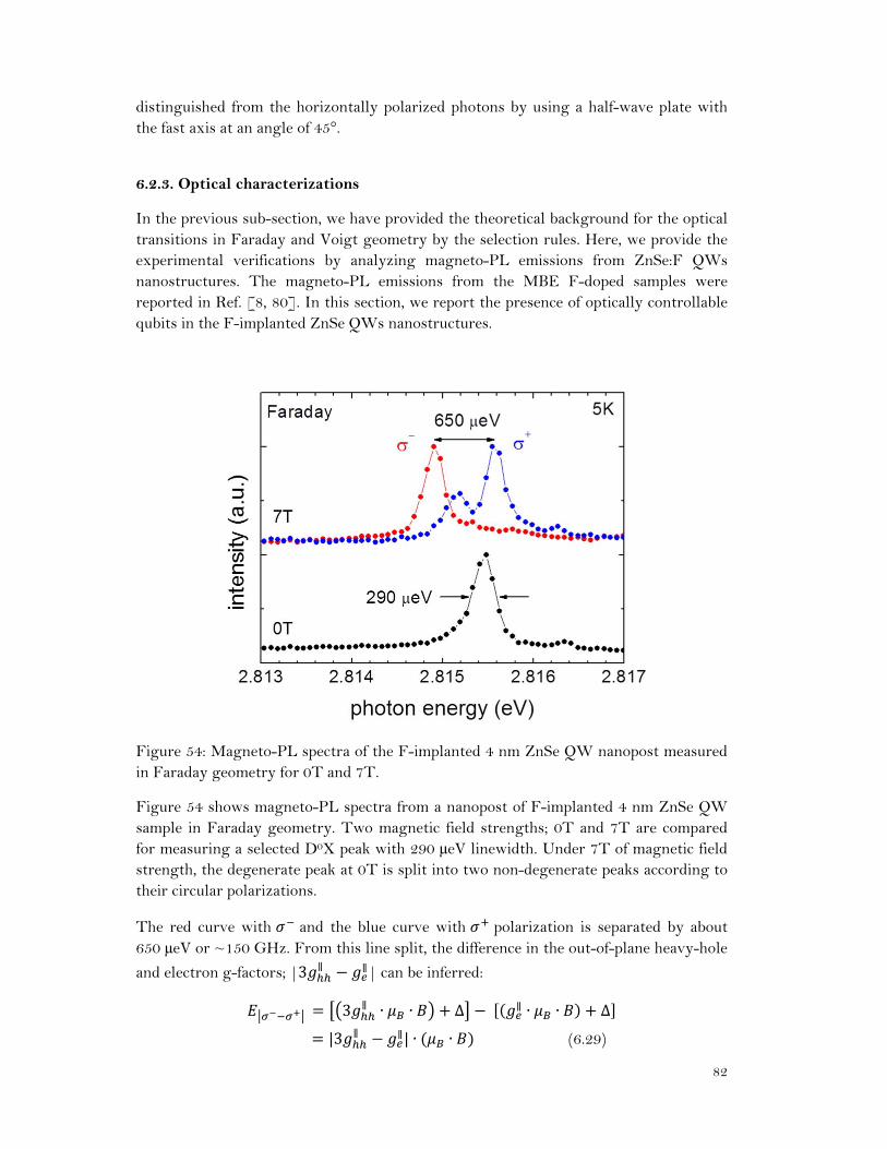
82
distinguished from the horizontally polarized photons by using a half-wave plate with the fast axis at an angle of 45°.
6.2.3. Optical characterizations
In the previous sub-section, we have provided the theoretical background for the optical transitions in Faraday and Voigt geometry by the selection rules. Here, we provide the experimental verifications by analyzing magneto-PL emissions from ZnSe:F QWs nanostructures. The magneto-PL emissions from the MBE F-doped samples were reported in Ref. [8, 80]. In this section, we report the presence of optically controllable qubits in the F-implanted ZnSe QWs nanostructures.
Figure 54: Magneto-PL spectra of the F-implanted 4 nm ZnSe QW nanopost measured in Faraday geometry for 0T and 7T.
Figure 54 shows magneto-PL spectra from a nanopost of F-implanted 4 nm ZnSe QW sample in Faraday geometry. Two magnetic field strengths; 0T and 7T are compared for measuring a selected D0X peak with 290 μeV linewidth. Under 7T of magnetic field strength, the degenerate peak at 0T is split into two non-degenerate peaks according to their circular polarizations.
The red curve with and the blue curve with polarization is separated by about 650 μeV or ~150 GHz. From this line split, the difference in the out-of-plane heavy-hole
and electron g-factors; |3 ∥ ∥| can be inferred:
3 ∥ ∙ ∙ ∆ ∥ ∙ ∙ ∆
|3 ∥ ∥| ∙ ∙ (6.29)
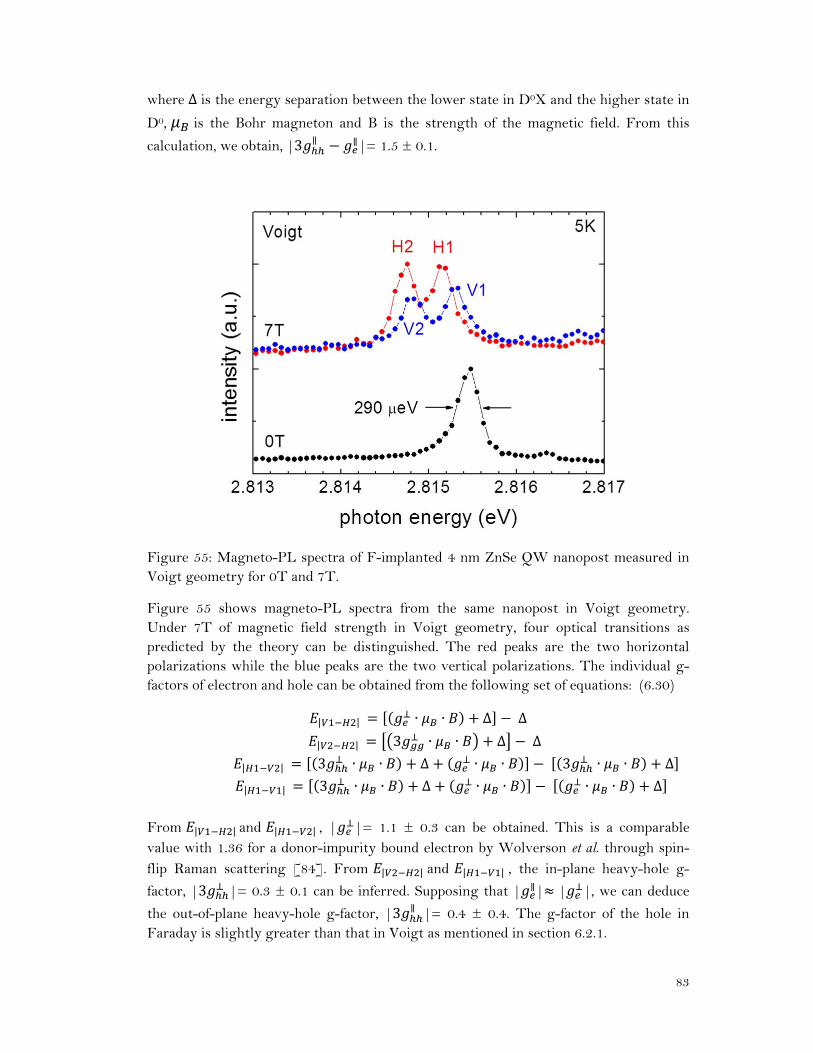
83
where ∆ is the energy separation between the lower state in D0X and the higher state in
D0, is the Bohr magneton and B is the strength of the magnetic field. From this
calculation, we obtain, |3 ∥ ∥|= 1.5 ± 0.1.
Figure 55: Magneto-PL spectra of F-implanted 4 nm ZnSe QW nanopost measured in Voigt geometry for 0T and 7T.
Figure 55 shows magneto-PL spectra from the same nanopost in Voigt geometry. Under 7T of magnetic field strength in Voigt geometry, four optical transitions as predicted by the theory can be distinguished. The red peaks are the two horizontal polarizations while the blue peaks are the two vertical polarizations. The individual g-factors of electron and hole can be obtained from the following set of equations: (6.30)
| | ∙ ∙ ∆ ∆
| | 3 ∙ ∙ ∆ ∆
| | 3 ∙ ∙ ∆ ∙ ∙ 3 ∙ ∙ ∆
| | 3 ∙ ∙ ∆ ∙ ∙ ∙ ∙ ∆ From | |and | |, | |= 1.1 ± 0.3 can be obtained. This is a comparable value with 1.36 for a donor-impurity bound electron by Wolverson et al. through spin-
flip Raman scattering [84]. From | |and | | , the in-plane heavy-hole g-
factor, |3 |= 0.3 ± 0.1 can be inferred. Supposing that | ∥| | |, we can deduce
the out-of-plane heavy-hole g-factor, |3 ∥ |= 0.4 ± 0.4. The g-factor of the hole in Faraday is slightly greater than that in Voigt as mentioned in section 6.2.1.
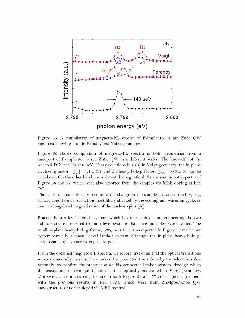
84
Figure 56: A compilation of magneto-PL spectra of F-implanted 4 nm ZnSe QW nanopost showing both in Faraday and Voigt geometry.
Figure 56 shows compilation of magneto-PL spectra in both geometries from a nanopost of F-implanted 4 nm ZnSe QW in a different wafer. The linewidth of the selected D0X peak is 140 μeV. Using equations in (6.9) in Voigt geometry, the in-plane
electron g-factor, | |= 1.1 ± 0.1, and the heavy-hole g-factor,| |= 0.0 ± 0.1 can be calculated. On the other hand, inconsistent diamagnetic shifts are seen in both spectra of Figure 56 and 57, which were also reported from the samples via MBE doping in Ref. [8]. The cause of this shift may be due to the change in the sample structural quality, e.g., surface condition or relaxation most likely affected by the cooling and warming cycle, or due to a long-lived magnetization of the nuclear spins [8]. Practically, a 3-level lambda system, which has one excited state connecting the two qubits states is preferred to multi-level systems that have multiple excited states. The
small in-plane heavy-hole g-factor, | |= 0.0 ± 0.1 as reported in Figure 57 makes our system virtually a quasi-3-level lambda system, although the in-plane heavy-hole g-factors can slightly vary from post-to-post. From the obtained magneto-PL spectra, we report first of all that the optical transitions we experimentally measured are indeed the predicted transitions by the selection rules. Secondly, we confirm the presence of doubly connected lambda system, through which the occupation of two qubit states can be optically controlled in Voigt geometry. Moreover, these measured g-factors in both Figure 56 and 57 are in good agreement with the previous results in Ref. [32], which were from ZnMgSe/ZnSe QW nanostructures fluorine doped via MBE method.
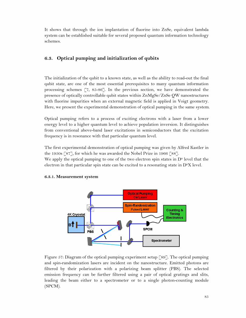
85
It shows that through the ion implantation of fluorine into ZnSe, equivalent lambda system can be established suitable for several proposed quantum information technology schemes.
6.3. Optical pumping and initialization of qubits
The initialization of the qubit to a known state, as well as the ability to read-out the final qubit state, are one of the most essential prerequisites to many quantum information processing schemes [7, 85-86]. In the previous section, we have demonstrated the presence of optically controllable qubit states within ZnMgSe/ZnSe QW nanostructures with fluorine impurities when an external magnetic field is applied in Voigt geometry. Here, we present the experimental demonstration of optical pumping in the same system. Optical pumping refers to a process of exciting electrons with a laser from a lower energy level to a higher quantum level to achieve population inversion. It distinguishes from conventional above-band laser excitations in semiconductors that the excitation frequency is in resonance with that particular quantum level. The first experimental demonstration of optical pumping was given by Alfred Kastler in the 1950s [87], for which he was awarded the Nobel Prize in 1966 [88]. We apply the optical pumping to one of the two electron spin states in D0 level that the electron in that particular spin state can be excited to a resonating state in D0X level. 6.3.1. Measurement system
Figure 57: Diagram of the optical pumping experiment setup [89]. The optical pumping and spin-randomization lasers are incident on the nanostructure. Emitted photons are filtered by their polarization with a polarizing beam splitter (PBS). The selected emission frequency can be further filtered using a pair of optical gratings and slits, leading the beam either to a spectrometer or to a single photon-counting module (SPCM).
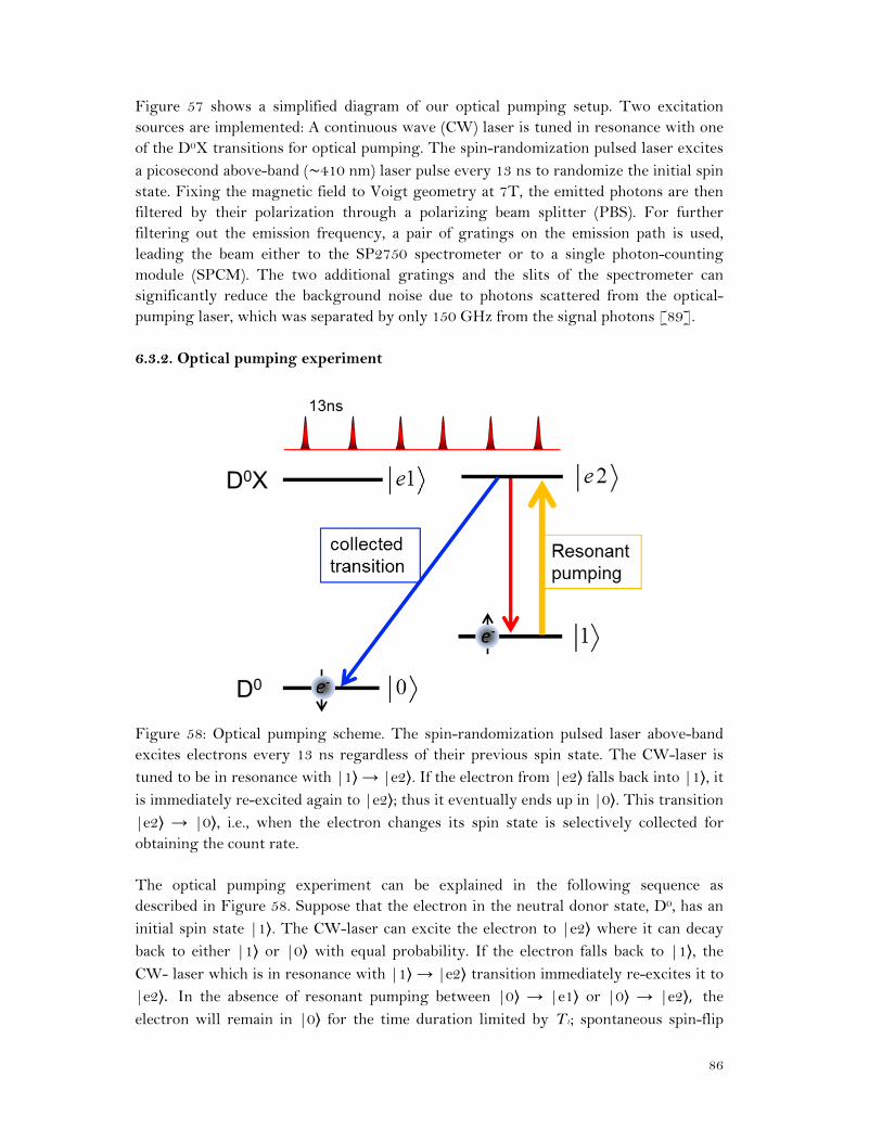
86
Figure 57 shows a simplified diagram of our optical pumping setup. Two excitation sources are implemented: A continuous wave (CW) laser is tuned in resonance with one of the D0X transitions for optical pumping. The spin-randomization pulsed laser excites a picosecond above-band (∼410 nm) laser pulse every 13 ns to randomize the initial spin state. Fixing the magnetic field to Voigt geometry at 7T, the emitted photons are then filtered by their polarization through a polarizing beam splitter (PBS). For further filtering out the emission frequency, a pair of gratings on the emission path is used, leading the beam either to the SP2750 spectrometer or to a single photon-counting module (SPCM). The two additional gratings and the slits of the spectrometer can significantly reduce the background noise due to photons scattered from the optical-pumping laser, which was separated by only 150 GHz from the signal photons [89]. 6.3.2. Optical pumping experiment
Figure 58: Optical pumping scheme. The spin-randomization pulsed laser above-band excites electrons every 13 ns regardless of their previous spin state. The CW-laser is tuned to be in resonance with |1 → |e2 . If the electron from |e2 falls back into |1 , it
is immediately re-excited again to |e2 ; thus it eventually ends up in |0 . This transition
|e2 → |0 , i.e., when the electron changes its spin state is selectively collected for obtaining the count rate. The optical pumping experiment can be explained in the following sequence as described in Figure 58. Suppose that the electron in the neutral donor state, D0, has an initial spin state |1 . The CW-laser can excite the electron to |e2 where it can decay back to either |1 or |0 with equal probability. If the electron falls back to |1 , the
CW- laser which is in resonance with |1 → |e2 transition immediately re-excites it to |e2 . In the absence of resonant pumping between |0 → |e1 or |0 → |e2 , the
electron will remain in |0 for the time duration limited by T1; spontaneous spin-flip
87
time, which is expected to be at least few ms [79]. For verifying the optical pumping effect, the transition|e2 → |0 , i.e., when the electron switches its spin, is selectively collected, then the count rates with or without optical pumping are compared. By accumulating these single photon emissions from many experiments, the optical pumping rate and the final population of state |0 can be determined. However, in order to accumulate the selective emission under the same condition every time, the experiment must be reset for each cycle. This is where the spin-randomization pulsed laser becomes necessary. The spin-randomization pulsed laser provides a picosecond above-band (∼410 nm) excitation with a repetition rate of 13 ns. Since the reported radiative recombination lifetime of a bound exciton is 100 ps [28], in every 13 ns, a “new” electron can be excited to|e1 or |e2 state, and then spontaneously falls to either of two spin states with approximately equal probability. We assign equal probability of the excited electron to occupy either |e1 or |e2 byassuming almost identical inter-subband oscillator strength: (6.31)
2 ∗
where is the energy deference between two excited states, and is the
envelope function of subband in the z-direction. By utilizing the envelope function
approximation (EFA), and |3 | 0; thus, almost no energy separation, the oscillator
strength in | → |e1 and | → |e2 becomes virtually identical where represents the initial excited state higher than |e1 and |e2 . Similar argument can be provided to the two spin states: | ↓ , | ↑ . The oscillator strength in the interband transition [90]; | → |1 is: (6.32)
, 2∗
| ∙ |
where , , and are the wavefunctions and the energies of the|1 and |
states respectively. is the unit vector in the electric field direction, and is the momentum operator [89]. Using the equivalent assumptions as in (6.12), we can deduce
that the oscillator strength is primarily proportional to . The energy splitting between two spin states under 7T is about 650 μeV, while the interband transition is about 2.815 eV. The ratio between these two energies is 0.023%, thus the difference in the oscillator strength would be negligible.
Considering the almost identical oscillator strength in the interband transition, we assume equal transition probabilities for the relevant optical transitions.
88
Figure 59: Approximated transition probabilities in respect to the presence of optical pumping: (a) Transition probabilities without CW-pumping, (b) transition probabilities with CW-pumping. Thus, without the CW-pumping laser, for each 13 ns cycle, there is 25% chance for each of the four optical transitions, as in Figure 59a from D0X → D0 to occur due to the spontaneous emission. As shown in Figure 59b, with the optical pumping laser, the electron in the two transitions |e1 → |1 and |e2 → |1 will be re-excited until it decays through|e2 →
|0 transition. The only transition which is unaffected by the optical pumping is |e1 →
|0 with 25% chance, thus the total probability for |e2 → |0 transition with the optical pumping mounts to be with 75% probability for each pulsed cycle. This theoretical prediction can be verified experimentally by comparing the measured count rate of single photons with optical pumping versus the count rate of single photons without the pumping. We define the ratio γ as: (6.34)
γ ≡ countrate withCW pumping
countrate withoutCW pumping, 1 3
The ratio γ can take a value between 1 and 3 representing no optical pumping effect and saturated optical pumping effect respectively. Prior to performing the optical pumping on a selected fluorine δ -doped 2 nm ZnMgSe/ZnSe QW nanostructure, we determined the electron and hole g-factors from this nanostructure to be [89]:
| | = 1.3 ± 0.3,
|3 | = 0.0 ± 0.1
| ∥ − ∥| = 0.9 ± 0.1
89
which is in good agreement with previous results. Furthermore, we observed a value of 0.22 ± 0.06 in the normalized two photon correlation function g(2)(τ) at zero delay (without background subtraction), which is well below the 0.5 threshold for a single emitter [89]. With these evidences from the same nanopost, we have strong confidence that the selected peak corresponds to the D0X to D0 transition of a single F-bound electron.
Figure: 60: Average count rate measured by different excitation sources. We measured 30.2 ± 0.8 average counts per seconds (cps) with only the spin-randomization laser on, i.e., no optical pumping and 95 ± 3 average cps when both lasers were applied. Figure 60 summarizes the measured average count rates by different excitation sources. We measured 30.2 ± 0.8 average counts per second (cps) with only the spin-randomization laser on, i.e., no optical pumping, and 13.0 ± 0.6 average cps with only the optical-pumping laser. When both lasers were applied, we measured 95 ± 3 average cps and a background of 0.2 ± 0.1 average cps when both lasers were turned off. These measurements were taken within the linear response region of the spectrometer CCD, and the count rate was calibrated against an optical power meter so that the spectrometer counts were proportional to the actual photon counts [89]. Using data from these experiments, we measure the optical pumping ratio γ to be (95 − 13.0)/(30.2 + 0.2) = 2.7 ± 0.1, indicating near saturation optical pumping. Moreover, we observed an optical pumping ratio γ larger than 2.3 when pumping on any of the four optical transitions showing the fully connected nature of our optical system.
90
6.4. Summary
We have investigated the behavior of bound electron spins by fluorine donor in ZnSe under an external magnetic field. A moderate magnetic field strength of 7T can yield the Zeeman splitting of 150 GHz between non-degenerate donor states. The spin-orbit coupling, as well as the conservation of angular momentum of photons prompts the allowed optical transitions to be determined by selection rules in Faraday and Voigt geometry. The predicted optical transitions are verified experimentally in magneto-PL spectra from F-implanted ZnSe QW nanostructures. We confirm the presence of doubly connected lambda system where the occupation of the two spin qubit states can be optically controlled in Voigt geometry. It shows that through the ion implantation of fluorine in ZnSe, equivalent lambda system can be established as in MBE doping. Furthermore, through the optical pumping experiment, we have demonstrated the ability to initialize the electron spin qubit as well as to read-out the final state showing fully-connected nature of our optical system. All of the above results are essential prerequisite for coherent optical manipulation of spin as qubit suitable for several proposed quantum information technology schemes.
91
Chapter 7
Summary and Outlook
Throughout this thesis, I have underlined the potentials of the bound electron in ZnSe:F system by experimentally demonstrating some of the demanded properties as qubits. In Chapter 3, I introduced the QW- confinement by growing a double heterostructure of ZnMgSe/ZnSe/ZnMgSe layers on GaAs for several benefits: The double ZnMgSe cladding layers prevent the carriers to leak into GaAs, but increase the likelihood of carriers falling into the ZnSe QW-potential. This induces an enhanced optical brightness due to the increased radiative recombination rate in the active zone. A relative reduction of the inhomogeneous broadening can be achieved in the samples with QWs by reducing the volume of the active zone. Furthermore, an increased binding energy of exciton was observed because of the compression of the donor wavefunction in the QWs with 3-4 nm in width. In Chapter 4, we have investigated conventional MBE fluorine doping method and reported a limitation of reaching the demanded doping level of 1017 - 1018 cm-3. This limitation is most likely caused by insufficient thermal dissociation of ZnF2; thus, we installed the ZnF2 cracker cell to achieve the necessary thermal dissociation establishing 19F molecular beam flux. As a result, we were able to modulate the doping level between 1015 cm-3 and 1018 cm-3 by doping temperature and doping mode. Alternatively, we have investigated the ion implantation of fluorine in ZnSe. We reported that with appropriate annealing procedures, the fluorine impurities can be incorporated as active donors in ZnSe QWs. The unique features that the ion implantation can provide such as: 1) the pure selection of 19F avoiding other non-desired elements, 2) more precise doping level control, 3) selective ion implantation, and 4) possibly registrations of single ions into undoped cavities, present the ion implantation of fluorine in ZnSe as an attractive choice for quantum information applications.
In the following chapter, I provided fabrication processes of ZnMgSe/ZnSe nanoposts in detail as means of isolating individual fluorine impurities. In order to optimize the structural and surface quality, the proximity effect and SeO2 clusters must be properly treated. The photoluminescence spectroscopy from F-implanted ZnSe QWs nanoposts was also investigated in Chapter 5. We have verified the ability to discreetly modulate the number of fluorine donors per pillar via ion implantation. Furthermore, Optical characteristics such as: 1) increasing number of D0X peaks in the PL spectrum with
92
higher implantation dose, and 2) the saturation behavior of D0X peaks, demonstrate successful ion implantation of fluorine as active donors. In Chapter 6, the behavior of bound electron spins in ZnSe under an external magnetic field was investigated. By applying a moderate magnetic field strength of 7T, non-degenerate donor states can be established by Zeeman splitting in the order of hundreds of 150 GHz. We have verified that the optical transitions available in Faraday and Voigt geometry indeed follow the selection rules. Moreover, we have confirmed the presence of optically controllable lambda system as in the MBE doped samples. Furthermore, through the optical pumping experiment, we have demonstrated the ability to initialize the electron spin qubit as well as to read-out the final state, showing fully-connected nature of our optical system.
This thesis conveys the ion implantation as an alternative doping method to MBE doping for establishing the bound electron spin states in ZnSe as qubits. While the photon emissions from MBE F-doped ZnMgSe/ZnSe QWs nanostructures have demonstrated as far as the photon anti-bunching of two single photons, and the entanglement, the F-implanted devices have yet to demonstrate these properties. Moreover, the next experimental lines would involve demonstration of coherent spin control through a two photon stimulated Raman transition by applying ultrafast optical signals, as shown in InGaAs QDs [8]. The similarity between our lambda system and that in InGaAs QDs suggests that an analogous approach may work for our system. Although it has been shown that an ensemble of fluorine donors in ZnSe features an electron spin dephasing times T2* is greater than 30 ns up to 40 K [27], the intrinsic decoherence time T2 from a single spin is yet to be measured. One of the potentials in our system regarding long lived Q-memory lies in the natural abundance of ½ nuclear spin of fluorine. Further research on the hyperfine interaction between electron and nuclear spin may extend the decoherence time significantly, as it is reported for P donor in Si. Furthermore, with the possibility of fluorine ion implantation, post-registration of fluorine impurities as active donors into undoped MBE grown ZnSe micro-, nano-cavities may construct a basis architecture of quantum repeaters.
The results presented in this thesis provide an overview of production → fabrication → characterization processes to demonstrate some of the qubit properties of bound electron spins to fluorine donors in ZnSe. Although there are still several advancements to be made to verge on other candidate systems as reliable qubits, based on the works presented in this thesis and further potentials to be realized, ZnSe:F system remains as an appealing solid-state based qubit candidate for quantum information science schemes.
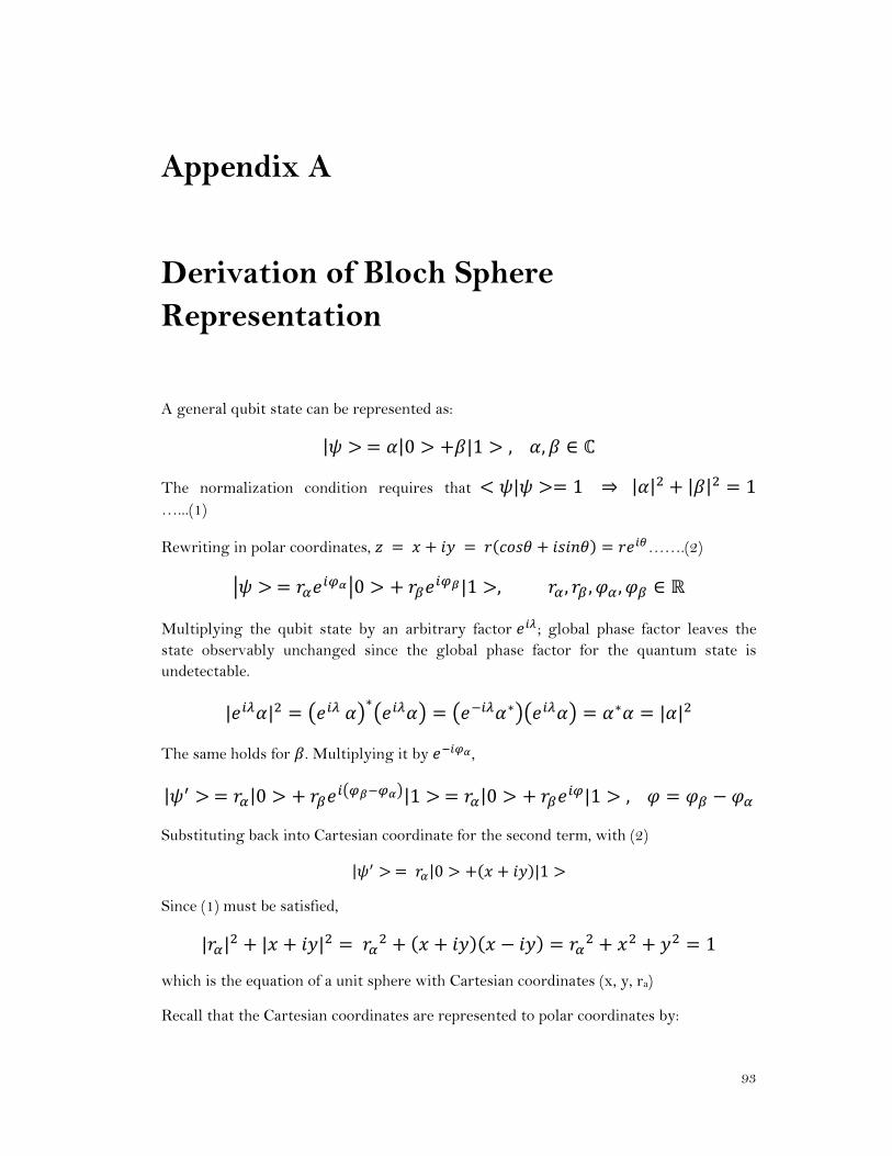
93
Appendix A
Derivation of Bloch Sphere Representation
A general qubit state can be represented as:
| |0 |1 , , ∈
The normalization condition requires that | 1 ⇒ | | | | 1 …...(1)
Rewriting in polar coordinates, …….(2)
0 |1 , , , , ∈
Multiplying the qubit state by an arbitrary factor ; global phase factor leaves the state observably unchanged since the global phase factor for the quantum state is undetectable.
| | ∗ ∗ ∗ | |
The same holds for . Multiplying it by ,
| |0 |1 |0 |1 ,
Substituting back into Cartesian coordinate for the second term, with (2)
| |0 |1
Since (1) must be satisfied,
| | | | 1
which is the equation of a unit sphere with Cartesian coordinates (x, y, ra)
Recall that the Cartesian coordinates are represented to polar coordinates by:
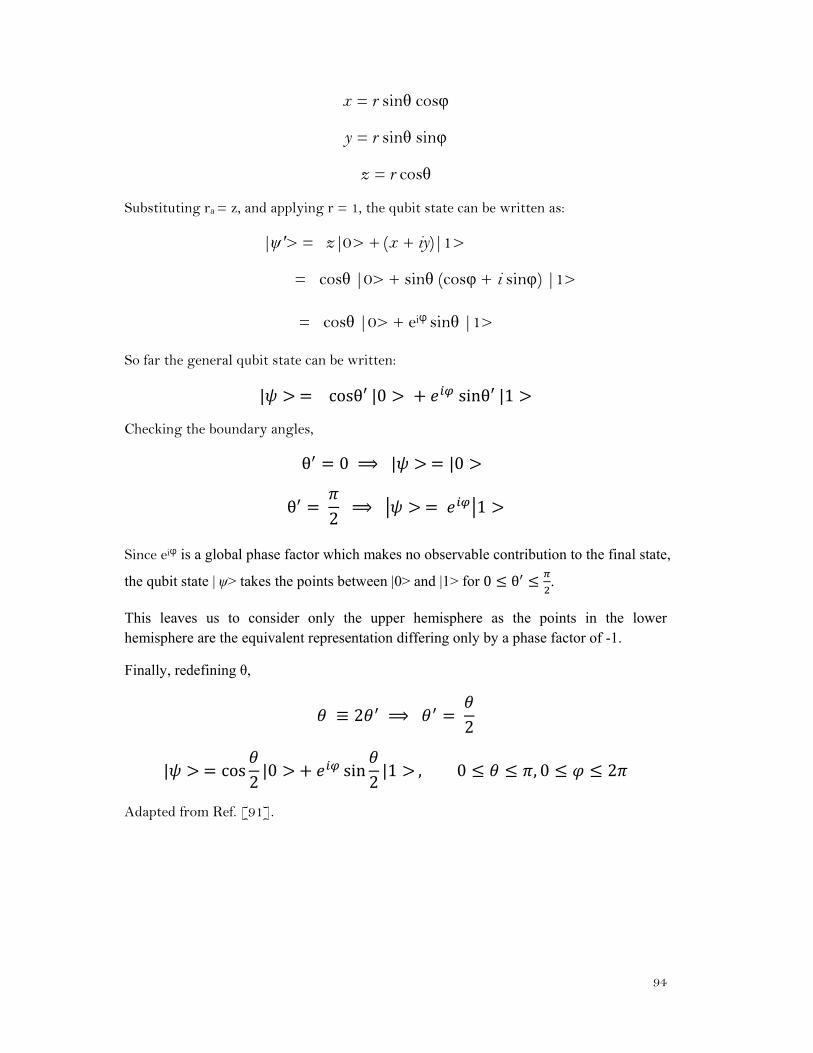
94
x = r sinθ cosφ
y = r sinθ sinφ
z = r cosθ
Substituting ra = z, and applying r = 1, the qubit state can be written as:
|ψ'> = z|0> + (x + iy)|1>
= cosθ |0> + sinθ (cosφ + i sinφ) |1>
= cosθ |0> + eiφ sinθ |1>
So far the general qubit state can be written:
| cosθ′|0 sinθ′|1
Checking the boundary angles,
θ 0 ⟹ | |0
θ 2⟹ 1
Since eiφ is a global phase factor which makes no observable contribution to the final state,
the qubit state | ψ> takes the points between |0> and |1> for 0 θ .
This leaves us to consider only the upper hemisphere as the points in the lower hemisphere are the equivalent representation differing only by a phase factor of -1.
Finally, redefining θ,
≡ 2 ⟹ 2
| cos2|0 sin
2|1 , 0 , 0 2
Adapted from Ref. [91].
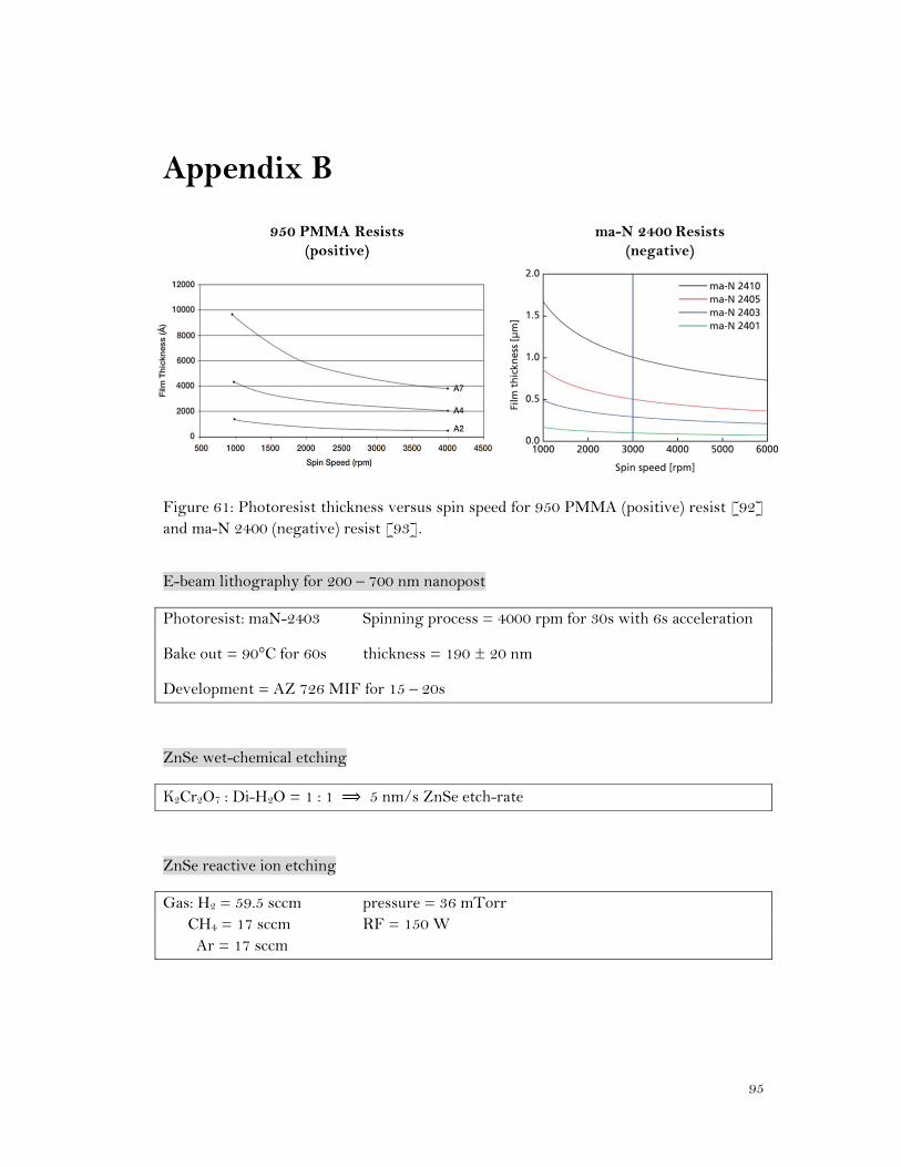
95
Appendix B
Figure 61: Photoresist thickness versus spin speed for 950 PMMA (positive) resist [92] and ma-N 2400 (negative) resist [93].
E-beam lithography for 200 – 700 nm nanopost
Photoresist: maN-2403 Spinning process = 4000 rpm for 30s with 6s acceleration
Bake out = 90°C for 60s thickness = 190 ± 20 nm
Development = AZ 726 MIF for 15 – 20s
ZnSe wet-chemical etching
K2Cr2O7 : Di-H2O = 1 : 1 ⟹ 5 nm/s ZnSe etch-rate
ZnSe reactive ion etching
Gas: H2 = 59.5 sccm pressure = 36 mTorr CH4 = 17 sccm RF = 150 W Ar = 17 sccm

96
GaAs undercut wet-chemical etching
NaOH : H2O2 = 41 : 9 Dilution = NaOH + H2O2 : Di-H2O = 1 : 5⟹ 10 nm/s GaAs etch-rate
Rapid thermal annealing
Temperature = 400°C duration = 30s + 8s (ramp) N2 overpressure
SiO2 passivation
SiH4/Ar = 124/100 sccm N2O = 50 sccm
Pressure = 425 mTorr RF = 10W temp. = 120°C rate= 45nm/min
Reactive Ion Etching of ZnSe
Ar = 17 sccm CH4 = 17 sccm H2 = 60 sccm RF = 150 W pressure = 35 mTorr temp. = 120°C etch rate = 14nm/min
97
Bibliography
[1] R. P. Poplavskii, Uspekhi Fizicheskikh Nauk,115:3, 465–501 [2] R.P. Feynman, Simulating Physics with computers, Int. J. Theor. Phys. 21, 467
(1982). [3] P. W. Shor, Proceedings, 35th Annual Symposium of Foundations of Computer
Science. IEEE Press (1994). [4] Buluta et al. Science. 326 108 (2010) [5] T. D. Ladd, F. Jelezko, R. Laflamme, Y. Nakamura, C. Monroe & J. L. O’Brien,
Quantum computers, Nature 464, 45-53 (4 March 2010) [6] A. Schreiber, A. Gábris, P. P. Rohde, K. Laiho, M. Štefaňák, V. Potocˇek, C.
Hamilton, I. Jex, C. Silberhorn, Science 336, 55 (2012) [7] David P. DiVincenzo, Fortschr. Phys. 48 (2000) 9-11, 771-783 [8] Susan M. Clark, Ph.D. Dissertation, Stanford University (2010). [9] Beugnon, J., Jones, M. P. A., Dingjan, J., Darquie, B., Messin, G., Browaeys, A., and
Grangier, P. Nature 440(7085), 779-782 (2006). [10] Maunz, P., Moehring, D. L., Olmschenk, S., Younge, K. C., Matsukevich, D. N.,
and Monroe, C. Nature Physics 3(8), 538-541 (2007). [11] Bollinger, J. J., Heinzen, D. J., Itano, W. M., Gilbert, S. L., and Wineland, D. J.
IEEE Trans. Insr. Meas. 40(2), 126-128 (1991). [12] Olmschenk, S., Matsukevic, D. N., Maunz, P., Hayes, D., Duan, L. M., Monroe, C.
Science 2009, 323, 486. [13] Seidelin, S., et al. Phys. Rev. Lett. 2006, 96, 253003. [14] D. Leibfried, R. Blatt, C. Monroe, and D. Wineland, Rev. Mod. Phys. 75. 281-324
(2003). [15] Greilich, A., Yakovlev, D. R., Shabaev, A., Efros, A. L., Yugova, I. A., Outlon, R.,
Stavarache, V., Reuter, D., Wieck, A., Bayer, M. Science 2006, 313, 341. [16] Santori, C., Fattal, D., Vuckovic, J., Solomon, G. S., Yamomoto, Y. Nature 2002,
419, 594.
98
[17] Press, D., De Greve, K., McMahon, P. L., Ladd, T. D., Friess, B., Schneider, C., Kamp, M., Hofling, S., Forchel, A., Yamomoto, Y. Nat. Photonics 2010, 4, 367.
[18] Patel, R. B., Bennett, A. J., Farrer, I., Nicoll, C. A., Ritchie, D. A., Shields, A. J.
Nat. Photonics 2010, 4, 632 [19] J. R. Petta, A. C. Johnson, J. M. Taylor, E. A. Laird, A. Yacoby, M. D. Lukin, C.
M. Marcus, M. P. Hanson, and A. C. Gossard, Science 309, 2180-2184 (2005). [20] Kurtsiefer, C., Mayer, S., Zarda, P., and Weinfurter, H. Phys. Rev. Lett. 85(2),
290-293 (2000). [21] Betalov, A., Zierl, C., Gaebel, T., Neumann, P., Chan, I., Balasubramanian, G.,
Hemmer, P. R., Jelezko, F., and Wrachtrup, J. Phys. Rev. Lett. 100(7), 077401 (2008).
[22] Balasubramanian, G. Et al., Nature Mater. 8, 383-387 (2009). [23] Koppens, F. H. K., Buizert, C., Tielrooij, K. J., Vink, I. T., Nowack, K. C., Meunier,
T., Kouwenhoven, K. P. & Vandersypen, L. M. K., Nature 442, 766 (2006). [24] Pawlis, A., Sanaka, K., Götzinger, S., Yamamoto, Y., and Lischka, K., Semicond.
Sci. Tech. 21(10), 1412-1415 (2006). [25] Dos Santos, L. S., Schmidt, W. G., Rauls, E., Phys. Rev. B 84(11), 115201 (2011). [26] Merz J. L., Kukimoto, H., Nassau, K., Shiever, J. W., Phys. Rev. B 6(2), 545-556,
(1972) [27] Greilich, A., Pawlis, A., Liu, F., Yugov, O. A., Yakovlev, D. R., Lischka, K.,
Yamamoto, Y., and Bayer, M. Phys. Rev. B 85(12), 121303R (2011). [28] Ladd, T. D., Press, D., De Greve, K., McMahon, P. L., Friess, B., Schneider, C.,
Kamp, M., Hofling, S., Forchel, A., Yamamoto, Y. Phys. Rev. Lett. 2010, 105, 107401
[29] Sanaka, K., Pawlis, A., Ladd, T. D., Lischka, K., Yamamoto, Y., Phys. Rev.
Lett.103, 053601 (2009). [30] Sanaka, K., Pawlis, A., Ladd. T. D., Sleiter, D. J., Lischka, K., Yamamoto, Y.,
Nano. Lett. 2012, 12, 4611 [31] Kim, Y. M., Sleiter, D., Sanaka, K., Yamamoto, Y., Meijer, J., Lischka, K., Pawlis,
A., Phys. Rev. B 85, 085302 (2012) [32] K. De Greve, S. M. Clark, D. Sleiter, K. Sanaka, T. D. Ladd, M. Panfilova, A.
Pawlis, K. Lischka, and Y. Yamamoto, Appl. Phys. Lett.97, 241913 (2010). [33] Nowack K. C., Koppens, F. H. L., Nazarov, Y. V. & Vandersypen, L. M. K.,
Science 318, 1430-1433 (2007). [34] Burkard, G., Loss, D. & DiVincenzo, D. P., Phys. Rev. B 59, 2070 (1999).
99
[35] Petta, J. R., Johnson, A. C., Taylor, J. M., Laird, E. A., Yacoby, A., Lukin, M. D.,
Marcus, C. M., Hanson, M. P. & Gossard, A. C., Science 309, 2180 (2005). [36] N. V. Bondar, V. V. Tishchenko and M. S. Brodin, Semiconductors, 34 (2000) 568. [37] A. M. Stoneham, Theory of Defects in Solids: Electronic Structure of Defects in
Insulators and Semiconductor, Great Britain, J. W. Arrowsmith Ltd, Bristol (1975).
[38] Pawlis, Alexander, Habilitation thesis, II-VI Semiconductor Nanosystems –
Applications in Quantum Information Science, University of Paderborn, (2012) [39] Wei, S. H. and Zunger, A. Appl. Phys. Lett. 72(16), 2011-2013 (1998). [40] Sim, E. D., Joh, Y. S., Min, S. I., Lee, C. D., and Chang, S. K. J. Cryst. Growth
177(3-4), 185-190 (1997) [41] Wörz, M., Griebl, E., Reisinger, T., Flierl, R., Haserer, B., Semmler, T., Frey, T.,
and Gebhardt, W. phys. Stat. Sol. (B) 202(2), 805-816 (1997). [42] Fox. Mark., Optical Properties of Solids, 2nd edition, Oxford Press, New York
(2010) [43] G. B. Astakhov, D. R. Yakovlev, V. P. Kocereshko, W. Ossau, J. Nürnberger, W. Faschinger, and G. Landwehr, Phys. Rev. B 60, R8485 (1999). [44] Bastard, G. Hydrogenic impurity states in a quantum well: A simple model. Phys. Rev. B 24, 4714 (1981). [45] Mikhail, I. F. I. & Ismail, I. M. M. Binding energy of an off-center hydro- genic donor impurity in finite confining potential quantum well. Acta Physica Polonica, A 111, 373 (2007). [46] Zrenner, A., Beham, E., Stufler, S., Findeis, F., Bichler, M., and Abstreiter, G.
Nature 418(6898), 612-614 (2002). [47] Michaelis De Vasconcellos, S., Gordon, S., Bichler, M., Meier, T., and Zrenner, A.
Nature Photonics 4(8), 545-548 (2010). [48] Greilich, A., Oulton, R., Zhukov, E. A., Yogova, I. A., Yakovlev, D. R., Bayer, M.,
Shabaev, A., Efros, A. L., Merkulov, I. A., Stavarache, V., Reuter, D., and Wieck, A. Phys. Rev. Lett. 96(22), 227401 (2006).
[49] Santori, C., Pelton, M., Solomon, G., Dale, Y., and Yamamoto, Y. Phys. Rev. Lett.
86(8), 1502-1505 (2001). [50] Wagner, J. and Ramsteiner, M. J. Appl. Phys. 62(5), 2148-2150 (1987).
100
[51] Yang. A., Steger, M., Karaiskaj, D., Thewalt, M. L. W., Cardona, M., Itoh, K. M., Riemann, H., Abrosimov, N. V., Churbanov, M. F., Gusev, A. V., Bulanov, A. D., Kaliteevskii, A. K., Godisov, O. N., Becker, P., Pohl, H. J., Ager, J. W., and Haller, E. E. Phys. Rev. Lett. 97(22), 227401 (2006).
[52] Tyryshkin, A. M., Lyon, S. A., Astashkin, A. V., and Raisimring, A. M. Phys. Rev.
B 68(19), 193207 (2003). [53] Kim, Y. M., Master thesis, Properties of Fluorine as Donor in ZnSe, Department
of Physics, University of Paderborn, (2010). [54] Y.C. Chen, P.K. Bhattacharya and J. Singh, Journal of Crystal Growth, 111,
228—232, (1991) [55] Y Horikoshi, Semicond. Sci. Technol. 8 1032 (1993) [56] K. Weißgerber, Bachelor thesis, University of Paderborn, (2010) [57] W. Lerch, phys. Stat. Sol. (a) 158, 117 (1996) [58] W. Shockley, "Semiconductor translating device," US Patent 2,666,814, filed 27
Apr. 1949. [59] R.S. Ohl, "Semiconductor translating device," US Patent 2,750,541, filed 31 Jan
1950. (Issued 12 June 1956) [60] J.W. Moyer, "Method of making p-n junction semiconductor unit," US Patent
2,842,466, filed 15 June 1954 (Issued 8 July 1958).
[61] W. Shockley, "Forming semiconductive devices by ionic bombardment," US Patent 2,787,564, filed 28 Oct 1954 (Issued 2 Apr 1957).
[62] S. Adachi and Y. Machi, J. Appl. Phys. 17 (1978) pp. 135-139
[63] P. L. Degen, phys. stat. sol. (a) 16, 9 (1973) [64] J. Meijer, S. Pezzagna, T. Vogel, B. Burchard, H. H. Bukow, I. W. Rangelow, Y.
Sarov, H. Wiggers, I. Pluemel, F. Jelezko, J. Wrachtrup, F. Schmidt-Kaler, W. Schnitzler, and K. Singer, Appl. Phys. A 91, 567 (2008).
[65] S. Pezzagna, D. Wildanger, P. Mazarov, A. D. Wieck, Y. Sarov, I. Rangeow, B.
Naydenov, F. Jelezko, K. W. Hell, and J. Meijer, Small 6, 2117 (2010). [66] T. Schenkel, A. Persaud, S. J. Park, J. Meijer, J. R. Kingsley, J. W. McDonald, J. P.
Holder, J. Bokor, and D. H. Schneider, J. Vac. Sci. Technol. B20, 2819 (2002). [67] J. Meijer, T. Vogel, B. Burchard, I. W. Rangelow, L. Bischo_, J. Wrachtrup, M.
Domhan, F. Jelezko, W. Schnitzler, S. A. Schulz, et al., Appl. Phys. A 83, 321 (2006).
[68] W. Schnitzler, N. M. Linke, R. Fickler, J. Meijer, F. Schmidt-Kaler, and K. Singer,
Phys. Rev. Lett. 102, 070501 (2009).
101
[69] J. Lindhard, R.1. Scharff, and H. E. Schiott. Mat. Fys. Hledd. Dan. Vid. Selsk. 33, No. 14 (1963).
[70] J. B. Smathers, E. Kneedler, B. R. Bennett, and B. T. Jonker, Appl. Phys. Lett. 72,
1238 (1998) [71] Nezih Unal, Electron Beam Lithography Proximity Effect and Correction
Technologies, powerpoint presentation, GeniSys Gmbh, Munich-Germany (2011). http://www.ecti.utoronto.ca/Assets/ECTI+Digital+Assets/Emerging+Communications+Technology+Institute/ECTI+Digital+Assets/Events/SummerInst/Slides-SummerInst-Unal-GenISys.pdf
[72] Maan M. Alkaisi and Khairudin Mohamed (2010). Three-Dimensional Patterning
Using Ultraviolet Nanoimprint Lithography, Lithography, Michael Wang (Ed.), ISBN: 978-953-307-064-3, InTech, DOI: 10.5772/8194. Available from: http://www.intechopen.com/books/lithography/three-dimensional-patterning-using-ultraviolet-nanoimprint-lithography
[73] Hideyuki Doi, Method of cleaning a surface a compound semiconductor crystal of
Group II-VI elements in periodic table, US Patent 6.001.744, filed 14 Dec 1999 [74] R. Ludeke, Solid State Commun. 24, 725 (1977). [75] A. Ebina, K. Asano, Y. Suda, and T. Takahaski, J Vac. Sci. Technol. 17, 1074
(1980). [76] A. Ebina, Y. Suda, and T. Takahashi, Int. J. Electron. 52, 77 (1982). [77] O. Kubaschewski and C. B. Alock, Metallurgical Thermochemistry, 5th ed.
(Pergamon, New York, 1979). [78] M. M. Montecchi and M. P. da Silva, Thin Solid Films 234, 557 (1993). [79] D. J. Sleiter, Ph.D. Dissertation, Optical pumping of single donor-bound electrons
in Zinc Selenide and Silicon, Stanford University, (2012) [80] F. Meier, B. P. Zakharchenya, Optical Orientation (North-Holland, Amsterdam,
1984)
[81] O. Madelung, Landolt-Bornstein, Intrinsic Properties of Group IV Elements and III-V, II-VI and I-VII Compounds (Springer, Berlin 1987)
[82] M. Oestreich, S. Hallstein, A. P. Heberle, K. Eberl, E. Bauser, W. W. Rühle, Phys. Rev. B 53, 7911 (1996)
[83] H. Hurwitz Jr. and R. C. Jones, Journal of the Optical Society of America 31 (7): 488–493, (1941)
[84] D. Wolverson, P. Boyce, C. Townsley, B. Schlichterle, and J. Davies, J. Cryst. Growth 159, 229 (1996)
102
[85] Ladd, T. D., Look, P., Nemoto, K., Munro, W. J., Yamamoto, Y., New J. Phys. 2006, 8, 184.
[86] Childress, L., Taylor, J. M., Sorensen, A. S., Lukin, M. D. Phys. Rev. A 2005, 72,
052330. [87] A. Kastler, J. Opt. Soc. Am, 47, 460-465 (1957). [88] Nobel Prize in Physics 1966 - Presentation Speech", nobelprize.org, 9 Aug., 2012,
http://www.nobelprize.org/nobel prizes/physics/laureates/1966/press.html [89] D. J. Sleiter, K. Sanaka, Y. M. Kim, K. Lischka, A. Pawlis, and Y. Yamamoto,
Nano Lett. 2013, 13, 116−120 [90] F. Janiak, G. Sęk, M. Motyka, K. Ryczko, J. Misiewicz, A. Bauer, S. Höfling, M.
Kamp, and A. Forchel, Appl. Phys. Lett. 100, 231908 (2012) [91] I. Glendinning, European Center for Parallel Computing at Vienna, (2005)
http://www.vcpc.univie.ac.at/~ian/hotlist/qc/talks/bloch-sphere.pdf [92] Micro Chem, NANO PMMA and Copolymer, provided PMMA data sheet, USA.
Available from: http://microchem.com/pdf/PMMA_Data_Sheet.pdf. [93] Micro resist technology GmbH, ma-N 2400 – Negative Tone Photoresist series,
provided data sheet, Germany. Available from: http://microchem.com/PDFs_MRT/ma-N%202400%20overview.pdf

103

104
γέγοναν. ἐγώ τὸ Α καὶ τὸ Ω, ἡ ἀρχὴ καὶ τὸ τέλος.
ΑΩ