Datasheet - TS488 - Pop-free 120 mW stereo headphone amplifier
32
Features • Pop and click noise protection circuitry • Operating range from VCC = 2.2 V to 5.5 V • Standby mode active low • Output power: – 120 mW at 5 V, into 16 Ω with 0.1% THD+N max. (1 kHz) – 55 mW at 3.3 V, into 16 Ω with 0.1% THD+N max. (1 kHz) • Low current consumption: 2.7 mA max. at 5 V • Ultra-low standby current consumption: 10 nA typical • High signal-to-noise ratio • High crosstalk immunity: 102 dB (F = 1 kHz) • PSRR: 70 dB typ. (F = 1 kHz), inputs grounded at 5 V • Unity-gain stable • Short-circuit protection circuitry • Available in DFN8 2x2 mm Applications • Headphone amplifiers • Mobile phones, PDAs, computer motherboards • High-end TVs, portable audio players Description The TS488 is a dual audio power amplifier capable of driving, in single-ended mode, either a 16 Ω or a 32 Ω stereo headset. The TS488 eliminates pop and click noise and reduces the number of required external passive components. Capable of descending to low voltages, it delivers up to 31 mW per channel (into 16 Ω loads) of continuous average power with 0.1% THD+N in the audio bandwidth from a 2.5 V power supply. An externally-controlled standby mode reduces the supply current to 10 nA (typ.). The unity gain stable is configured by external gain-setting resistors. Product status link TS488 Product summary Order code TS488IQT Temperature range -40 to +85 °C Package DFN8 2x2 mm Packing Tape and reel Marking K88 Pop-free 120 mW stereo headphone amplifier TS488 Datasheet DS4579 - Rev 8 - May 2020 For further information contact your local STMicroelectronics sales office. www.st.com
Transcript of Datasheet - TS488 - Pop-free 120 mW stereo headphone amplifier
Features
• Pop and click noise protection circuitry• Operating range from VCC = 2.2 V to 5.5 V• Standby mode active low• Output power:
– 120 mW at 5 V, into 16 Ω with 0.1% THD+N max. (1 kHz)– 55 mW at 3.3 V, into 16 Ω with 0.1% THD+N max. (1 kHz)
• Low current consumption: 2.7 mA max. at 5 V• Ultra-low standby current consumption: 10 nA typical• High signal-to-noise ratio• High crosstalk immunity: 102 dB (F = 1 kHz)• PSRR: 70 dB typ. (F = 1 kHz), inputs grounded at 5 V• Unity-gain stable• Short-circuit protection circuitry• Available in DFN8 2x2 mm
Applications
• Headphone amplifiers• Mobile phones, PDAs, computer motherboards• High-end TVs, portable audio players
DescriptionThe TS488 is a dual audio power amplifier capable of driving, in single-ended mode,either a 16 Ω or a 32 Ω stereo headset.
The TS488 eliminates pop and click noise and reduces the number of requiredexternal passive components.
Capable of descending to low voltages, it delivers up to 31 mW per channel (into 16Ω loads) of continuous average power with 0.1% THD+N in the audio bandwidth froma 2.5 V power supply.
An externally-controlled standby mode reduces the supply current to 10 nA (typ.).The unity gain stable is configured by external gain-setting resistors.
Product status link
TS488
Product summary
Order code TS488IQT
Temperaturerange -40 to +85 °C
Package DFN8 2x2 mm
Packing Tape and reel
Marking K88
Pop-free 120 mW stereo headphone amplifier
TS488
Datasheet
DS4579 - Rev 8 - May 2020For further information contact your local STMicroelectronics sales office.
www.st.com
1 Typical application schematic
Figure 1. Typical application for the TS488
TS488=stdby
Stdby active low
1
2
8
5
7
4
6
3
Table 1. Application component information
Component Functional description
Rin1,2Inverting input resistor that sets the closed loop gain in conjunction with Rfeed.
This resistor also forms a high pass filter with Cin [Fc = 1 / (2 x Pi x Rin x Cin)]
Cin1,2 Input coupling capacitor that blocks the DC voltage at the amplifier input terminal
Rfeed1,2Feedback resistor that sets the closed loop gain in conjunction with Rin.
AV= closed loop gain= -Rfeed/Rin
Cs Supply output capacitor that provides power supply filtering
Cb Bypass capacitor that provides half supply filtering
Cout1,2Output coupling capacitor that blocks the DC voltage at the load input terminal.
This capacitor also forms a high pass with RL [Fc = 1 / (2 x Pi x RL x Cout)]
TS488Typical application schematic
DS4579 - Rev 8 page 2/32
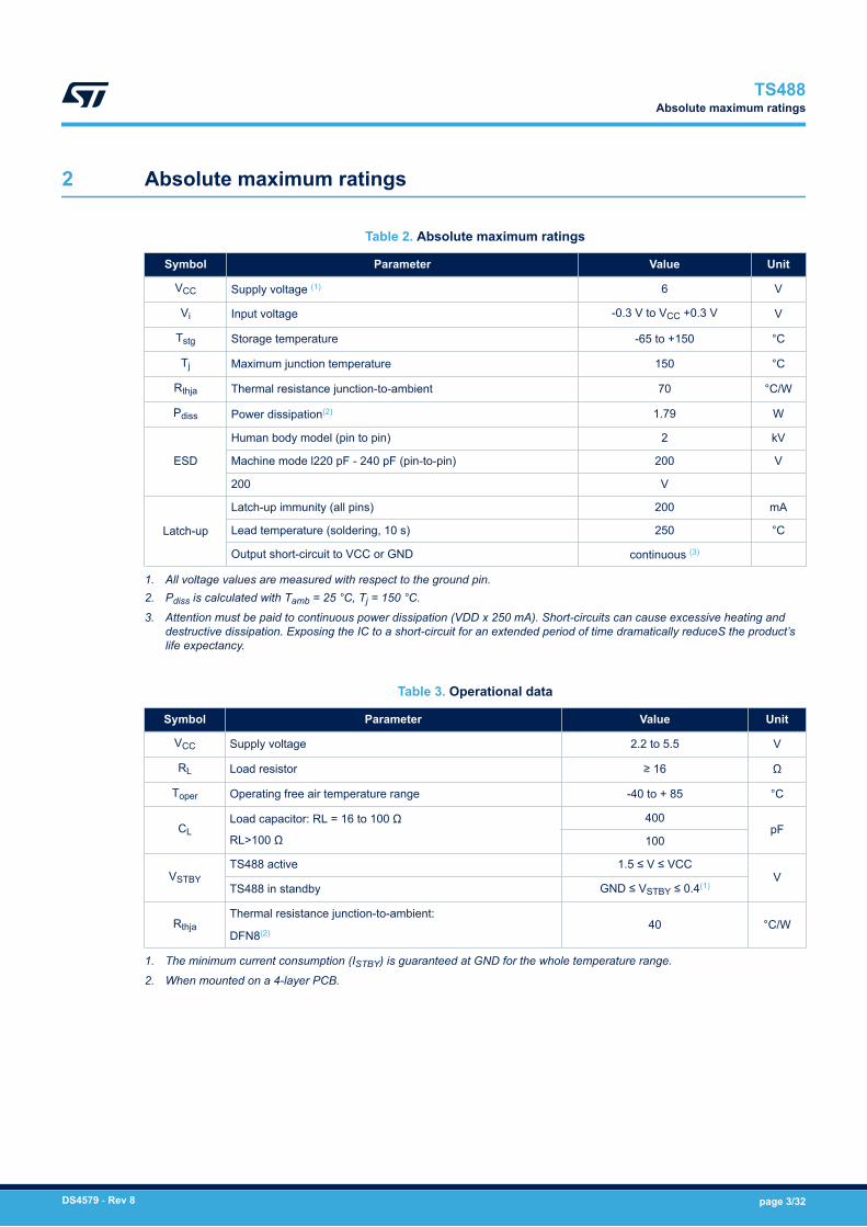
2 Absolute maximum ratings
Table 2. Absolute maximum ratings
Symbol Parameter Value Unit
VCC Supply voltage (1) 6 V
Vi Input voltage -0.3 V to VCC +0.3 V V
Tstg Storage temperature -65 to +150 °C
Tj Maximum junction temperature 150 °C
Rthja Thermal resistance junction-to-ambient 70 °C/W
Pdiss Power dissipation(2) 1.79 W
ESD
Human body model (pin to pin) 2 kV
Machine mode l220 pF - 240 pF (pin-to-pin) 200 V
200 V
Latch-up
Latch-up immunity (all pins) 200 mA
Lead temperature (soldering, 10 s) 250 °C
Output short-circuit to VCC or GND continuous (3)
1. All voltage values are measured with respect to the ground pin.2. Pdiss is calculated with Tamb = 25 °C, Tj = 150 °C.
3. Attention must be paid to continuous power dissipation (VDD x 250 mA). Short-circuits can cause excessive heating anddestructive dissipation. Exposing the IC to a short-circuit for an extended period of time dramatically reduceS the product’slife expectancy.
Table 3. Operational data
Symbol Parameter Value Unit
VCC Supply voltage 2.2 to 5.5 V
RL Load resistor ≥ 16 Ω
Toper Operating free air temperature range -40 to + 85 °C
CLLoad capacitor: RL = 16 to 100 Ω
RL>100 Ω
400pF
100
VSTBYTS488 active 1.5 ≤ V ≤ VCC
VTS488 in standby GND ≤ VSTBY ≤ 0.4(1)
RthjaThermal resistance junction-to-ambient:
DFN8(2)40 °C/W
1. The minimum current consumption (ISTBY) is guaranteed at GND for the whole temperature range.
2. When mounted on a 4-layer PCB.
TS488Absolute maximum ratings
DS4579 - Rev 8 page 3/32
3 Electrical characteristics
Table 4. Electrical characteristics at VCC=+5 V with GND =0 V, Tamb= 25 °C (unless otherwise specified)
Symbol Parameter Conditions Min. Typ. Max. Unit
ICC Supply current No input signal, no load 2 2.7 mA
ISTBY Standby current No input signal, VSTBY = GND RL = 32 Ω 10 1000 nA
Pout Output power
THD+N = 0.1% max., F = 1 kHz, RL = 32 Ω 75
mWTHD+N = 1% max. F = 1 kHz, RL = 32 Ω 70 80
THD+N = 0.1% max., F = 1 kHz, RL = 16 Ω 120
THD+N = 1% max., F = 1 kHz, RL = 16 Ω 100 130
THD+N Total harmonic distortion +noise
AV=-1, RL = 32 Ω, Pout = 60 mW, 20 Hz ≤ F ≤ 20 kHz 0.3%
AV=-1, RL = 16 Ω, Pout = 90 mW, 20 Hz ≤ F ≤ 20 kHz 0.3
PSRR Power supply rejectionratio, inputs grounded(1)
AV=-1, RL ≥ 16 Ω, Cb=1 µF, F = 1 kHz, Vripple = 200 mVpp 64 70dBAV=-1, RL ≥ 16 Ω, Cb=1 µF, F = 217 kHz, Vripple = 200
mVpp 62 68
VO Output swing
VOL: RL = 32 Ω 0.23 0.31
VVOH: RL = 32 Ω 4.53 4.72
VOL: RL = 16 Ω 0.44 0.57
VOH: RL = 16 Ω 4.18 4.48
SNR Signal-to-noise ratio A-weighted, AV=-1, RL = 32 Ω, THD+N < 0.4%, 20 Hz ≤ F ≤20 kHz 105 dB
Crosstalk Channel separationRL = 32 Ω, AV = -1, F = 1 kHz, F = 20 Hz to 20 kHz -102
dBRL = 32 Ω, AV = -1, F = 1 kHz, F = 20 Hz to 20 kHz -84
Ci Input capacitance 1 pF
GBP Gain bandwidth product RL = 32 Ω 1.1 MHz
SR Slew rate, unity gaininverting RL = 16 Ω 0.65 V/µs
VIO Input offset voltage Vicm=VCC/2 1 20 mV
twu Wake-up time 100 ms
1. Guaranteed by design and evaluation.
TS488Electrical characteristics
DS4579 - Rev 8 page 4/32
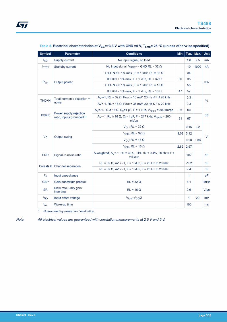
Table 5. Electrical characteristics at VCC=+3.3 V with GND =0 V, Tamb= 25 °C (unless otherwise specified)
Symbol Parameter Conditions Min. Typ. Max. Unit
ICC Supply current No input signal, no load 1.8 2.5 mA
ISTBY Standby current No input signal, VSTBY = GND RL = 32 Ω 10 1000 nA
Pout Output power
THD+N = 0.1% max., F = 1 kHz, RL = 32 Ω 34
mWTHD+N = 1% max. F = 1 kHz, RL = 32 Ω 30 35
THD+N = 0.1% max., F = 1 kHz, RL = 16 Ω 55
THD+N = 1% max, F = 1 kHz, RL = 16 Ω 47 57
THD+N Total harmonic distortion +noise
AV=-1, RL = 32 Ω, Pout = 16 mW, 20 Hz ≤ F ≤ 20 kHz 0.3%
AV=-1, RL = 16 Ω, Pout = 35 mW, 20 Hz ≤ F ≤ 20 kHz 0.3
PSRR Power supply rejectionratio, inputs grounded(1)
AV=-1, RL ≥ 16 Ω, Cb=1 µF, F = 1 kHz, Vripple = 200 mVpp 63 69dBAV=-1, RL ≥ 16 Ω, Cb=1 µF, F = 217 kHz, Vripple = 200
mVpp 61 67
VO Output swing
VOL: RL = 32 Ω 0.15 0.2
VVOH: RL = 32 Ω 3.03 3.12
VOL: RL = 16 Ω 0.28 0.36
VOH: RL = 16 Ω 2.82 2.97
SNR Signal-to-noise ratio A-weighted, AV=-1, RL = 32 Ω, THD+N < 0.4%, 20 Hz ≤ F ≤20 kHz 102 dB
Crosstalk Channel separationRL = 32 Ω, AV = -1, F = 1 kHz, F = 20 Hz to 20 kHz -102 dB
RL = 32 Ω, AV = -1, F = 1 kHz, F = 20 Hz to 20 kHz -84 dB
Ci Input capacitance 1 pF
GBP Gain bandwidth product RL = 32 Ω 1.1 MHz
SR Slew rate, unity gaininverting RL = 16 Ω 0.6 V/µs
VIO Input offset voltage Vicm=VCC/2 1 20 mV
twu Wake-up time 100 ms
1. Guaranteed by design and evaluation.
Note: All electrical values are guaranteed with correlation measurements at 2.5 V and 5 V.
TS488Electrical characteristics
DS4579 - Rev 8 page 5/32
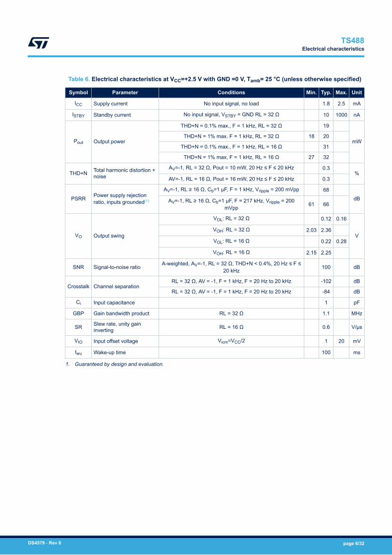
Table 6. Electrical characteristics at VCC=+2.5 V with GND =0 V, Tamb= 25 °C (unless otherwise specified)
Symbol Parameter Conditions Min. Typ. Max. Unit
ICC Supply current No input signal, no load 1.8 2.5 mA
ISTBY Standby current No input signal, VSTBY = GND RL = 32 Ω 10 1000 nA
Pout Output power
THD+N = 0.1% max., F = 1 kHz, RL = 32 Ω 19
mWTHD+N = 1% max. F = 1 kHz, RL = 32 Ω 18 20
THD+N = 0.1% max., F = 1 kHz, RL = 16 Ω 31
THD+N = 1% max, F = 1 kHz, RL = 16 Ω 27 32
THD+N Total harmonic distortion +noise
AV=-1, RL = 32 Ω, Pout = 10 mW, 20 Hz ≤ F ≤ 20 kHz 0.3%
AV=-1, RL = 16 Ω, Pout = 16 mW, 20 Hz ≤ F ≤ 20 kHz 0.3
PSRR Power supply rejectionratio, inputs grounded(1)
AV=-1, RL ≥ 16 Ω, Cb=1 µF, F = 1 kHz, Vripple = 200 mVpp 68dBAV=-1, RL ≥ 16 Ω, Cb=1 µF, F = 217 kHz, Vripple = 200
mVpp 61 66
VO Output swing
VOL: RL = 32 Ω 0.12 0.16
VVOH: RL = 32 Ω 2.03 2.36
VOL: RL = 16 Ω 0.22 0.28
VOH: RL = 16 Ω 2.15 2.25
SNR Signal-to-noise ratio A-weighted, AV=-1, RL = 32 Ω, THD+N < 0.4%, 20 Hz ≤ F ≤20 kHz 100 dB
Crosstalk Channel separationRL = 32 Ω, AV = -1, F = 1 kHz, F = 20 Hz to 20 kHz -102 dB
RL = 32 Ω, AV = -1, F = 1 kHz, F = 20 Hz to 20 kHz -84 dB
Ci Input capacitance 1 pF
GBP Gain bandwidth product RL = 32 Ω 1.1 MHz
SR Slew rate, unity gaininverting RL = 16 Ω 0.6 V/µs
VIO Input offset voltage Vicm=VCC/2 1 20 mV
twu Wake-up time 100 ms
1. Guaranteed by design and evaluation.
TS488Electrical characteristics
DS4579 - Rev 8 page 6/32
4 Electrical characteristics curves
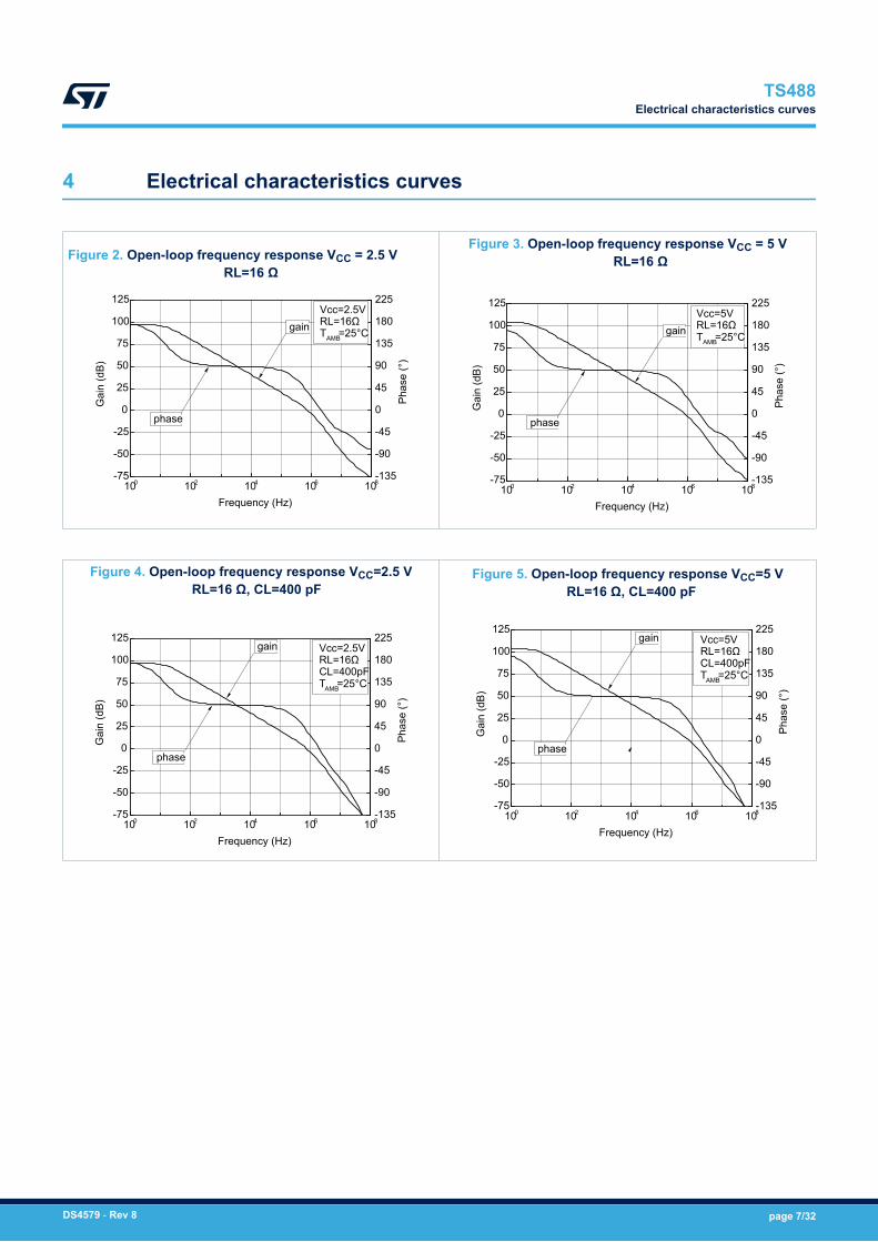
Figure 2. Open-loop frequency response VCC = 2.5 V RL=16 Ω
100 102 104 106 108-75
-50
-25
0
25
50
75
100
125
-135
-90
-45
0
45
90
135
180
225
gain
phase
Vcc=2.5VRL=16ΩTAMB=25°C
Gai
n (d
B)
Frequency (Hz)
Pha
se (°
)
Figure 3. Open-loop frequency response VCC = 5 V RL=16 Ω
100 102 104 106 108-75
-50
-25
0
25
50
75
100
125
-135
-90
-45
0
45
90
135
180
225
gain
phase
Vcc=5VRL=16ΩTAMB=25°C
Gai
n (d
B)
Frequency (Hz)
Pha
se (°
)
Figure 4. Open-loop frequency response VCC=2.5 V RL=16 Ω, CL=400 pF
100 102 104 106 108-75
-50
-25
0
25
50
75
100
125
-135
-90
-45
0
45
90
135
180
225gain
phase
Vcc=2.5VRL=16ΩCL=400pFTAMB=25°C
Gai
n (d
B)
Frequency (Hz)
Pha
se (°
)
Figure 5. Open-loop frequency response VCC=5 V RL=16 Ω, CL=400 pF
100 102 104 106 108-75
-50
-25
0
25
50
75
100
125
-135
-90
-45
0
45
90
135
180
225gain
phase
Vcc=5VRL=16ΩCL=400pFTAMB=25°C
Gai
n (d
B)
Frequency (Hz)
Pha
se (°
)
TS488Electrical characteristics curves
DS4579 - Rev 8 page 7/32
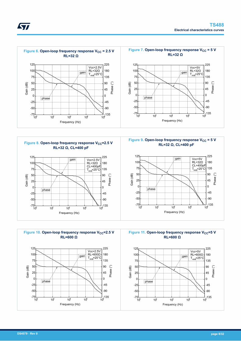
Figure 6. Open-loop frequency response VCC = 2.5 V RL=32 Ω
100 102 104 106 108-75
-50
-25
0
25
50
75
100
125
-135
-90
-45
0
45
90
135
180
225
gain
phase
Vcc=2.5VRL=32ΩTAMB=25°C
Gai
n (d
B)
Frequency (Hz)
Pha
se (°
)
Figure 7. Open-loop frequency response VCC = 5 V RL=32 Ω
100 102 104 106 108-75
-50
-25
0
25
50
75
100
125
-135
-90
-45
0
45
90
135
180
225
gain
phase
Vcc=5VRL=32ΩTAMB=25°C
Gai
n (d
B)
Frequency (Hz)
Pha
se (°
)
Figure 8. Open-loop frequency response VCC=2.5 V RL=32 Ω, CL=400 pF
100 102 104 106 108-75
-50
-25
0
25
50
75
100
125
-135
-90
-45
0
45
90
135
180
225gain
phase
Vcc=2.5VRL=32ΩCL=400pFTAMB=25°C
Gai
n (d
B)
Frequency (Hz)
Pha
se (°
)
Figure 9. Open-loop frequency response VCC = 5 V RL=32 Ω, CL=400 pF
100 102 104 106 108-75
-50
-25
0
25
50
75
100
125
-135
-90
-45
0
45
90
135
180
225gain
phase
Vcc=5VRL=32ΩCL=400pFTAMB=25°C
Gai
n (d
B)
Frequency (Hz) P
hase
(°)
Figure 10. Open-loop frequency response VCC=2.5 VRL=600 Ω
100 102 104 106 108-75
-50
-25
0
25
50
75
100
125
-135
-90
-45
0
45
90
135
180
225
gain
phase
Vcc=2.5VRL=600ΩTAMB=25°C
Gai
n (d
B)
Frequency (Hz)
Pha
se (°
)
Figure 11. Open-loop frequency response VCC=5 VRL=600 Ω
100 102 104 106 108-75
-50
-25
0
25
50
75
100
125
-135
-90
-45
0
45
90
135
180
225
gain
phase
Vcc=5VRL=600ΩTAMB=25°C
Gai
n (d
B)
Frequency (Hz)
Pha
se (°
)
TS488Electrical characteristics curves
DS4579 - Rev 8 page 8/32
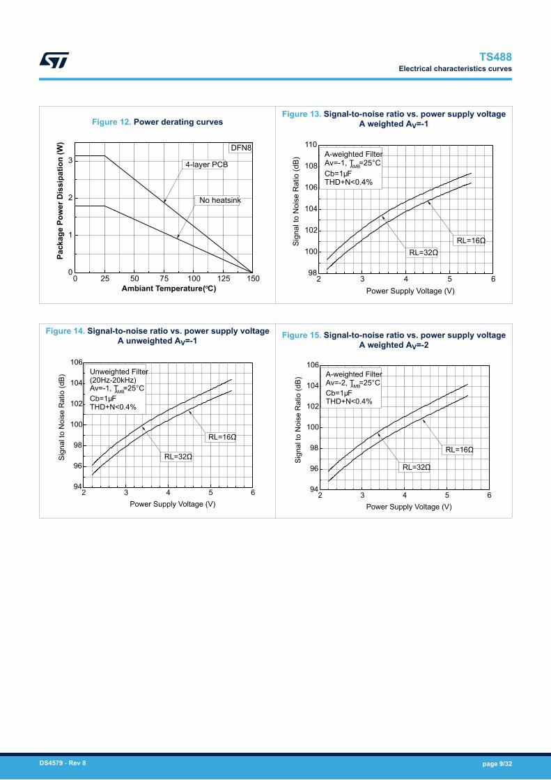
Figure 12. Power derating curves
0 25 50 75 100 125 1500
1
2
3 4-layer PCB
DFN8
No heatsink
Pack
age
Pow
er D
issi
patio
n (W
)
Ambiant Temperature (°C)
Figure 13. Signal-to-noise ratio vs. power supply voltageA weighted AV=-1
2 3 4 5 698
100
102
104
106
108
110
RL=32Ω
A-weighted FilterAv=-1, TAMB=25°CCb=1μFTHD+N<0.4%
Sign
al to
Noi
se R
atio
(dB)
Power Supply Voltage (V)
RL=16Ω
Figure 14. Signal-to-noise ratio vs. power supply voltageA unweighted AV=-1
2 3 4 5 694
96
98
100
102
104
106
RL=32Ω
Unweighted Filter (20Hz-20kHz)Av=-1, TAMB=25°CCb=1μFTHD+N<0.4%
Sign
al to
Noi
se R
atio
(dB)
Power Supply Voltage (V)
RL=16Ω
Figure 15. Signal-to-noise ratio vs. power supply voltageA weighted AV=-2
2 3 4 5 694
96
98
100
102
104
106
RL=32Ω
A-weighted FilterAv=-2, TAMB=25°CCb=1μFTHD+N<0.4%
Sign
al to
Noi
se R
atio
(dB)
Power Supply Voltage (V)
RL=16Ω
TS488Electrical characteristics curves
DS4579 - Rev 8 page 9/32
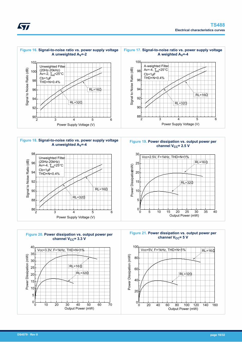
Figure 16. Signal-to-noise ratio vs. power supply voltageA unweighted AV=-2
2 3 4 5 690
92
94
96
98
100
102
RL=32Ω
Unweighted Filter (20Hz-20kHz)Av=-2, TAMB=25°CCb=1μFTHD+N<0.4%
Sign
al to
Noi
se R
atio
(dB)
Power Supply Voltage (V)
RL=16Ω
Figure 17. Signal-to-noise ratio vs. power supply voltageA weighted AV=-4
2 3 4 5 688
90
92
94
96
98
100
RL=32Ω
A-weighted FilterAv=-4, TAMB=25°CCb=1μFTHD+N<0.4%
Sign
al to
Noi
se R
atio
(dB)
Power Supply Voltage (V)
RL=16Ω
Figure 18. Signal-to-noise ratio vs. power supply voltageA unweighted AV=-4
2 3 4 5 686
88
90
92
94
96
98
RL=32Ω
Unweighted Filter (20Hz-20kHz)Av=-4, TAMB=25°CCb=1μFTHD+N<0.4%
Sign
al to
Noi
se R
atio
(dB)
Power Supply Voltage (V)
RL=16Ω
Figure 19. Power dissipation vs. output power perchannel VCC= 2.5 V
0 5 10 15 20 25 30 35 400
5
10
15
20
25
30
RL=32Ω
RL=16ΩVcc=2.5V, F=1kHz, THD+N<1%
Pow
er D
issi
patio
n (mW
)
Output Power (mW)
Figure 20. Power dissipation vs. output power perchannel VCC= 3.3 V
0 10 20 30 40 50 60 700
5
10
15
20
25
30
35
40
RL=32Ω
RL=16Ω
Vcc=3.3V, F=1kHz, THD+N<1%
Pow
er D
issi
patio
n (m
W)
Output Power (mW)
Figure 21. Power dissipation vs. output power perchannel VCC= 5 V
0 20 40 60 80 100 120 140 1600
20
40
60
80
100
RL=32Ω
RL=16ΩVcc=5V, F=1kHz, THD+N<1%
Pow
er D
issi
patio
n (m
W)
Output Power (mW)
TS488Electrical characteristics curves
DS4579 - Rev 8 page 10/32
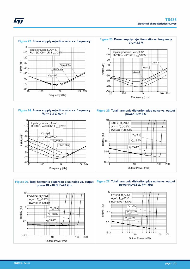
Figure 22. Power supply rejection ratio vs. frequency
100 1k 10k-80
-70
-60
-50
-40
-30
-20
-10
0
Vcc=5V
Vcc=3.3V
20k20
Vcc=2.5V
Inputs grounded, Av=-1, RL=16Ω, Cb=1μF, T AMB=25°C
PSR
R (d
B)
Frequency (Hz)
Figure 23. Power supply rejection ratio vs. frequencyVCC= 3.3 V
100 1k 10k-80
-70
-60
-50
-40
-30
-20
-10
0
Av=-4
Av=-1
20k20
Av=-2
Inputs grounded, Vcc=3.3V, RL=16Ω, Cb=1μF, T AMB=25°C
PSR
R (d
B)
Frequency (Hz)
Figure 24. Power supply rejection ratio vs. frequencyVCC= 3.3 V, AV= -1
100 1k 10k-80
-70
-60
-50
-40
-30
-20
-10
0
Cb=1μF
Cb=100nF
Cb=470nF
20k20
Cb=220nF
Inputs grounded, Av=-1, RL=16Ω, Vcc=3.3V, T AMB=25°C
PSR
R (d
B)
Frequency (Hz)
Figure 25. Total harmonic distortion plus noise vs. outputpower RL=16 Ω
1 10 1001E-3
0.01
0.1
1
10
VCC=3.3V
VCC=5V
VCC=2.5V
F=1kHz, RL=16ΩAV=-1, TAMB=25°CBW=20Hz-120kHz
THD
+N (%
)
Output Power (mW)200
Figure 26. Total harmonic distortion plus noise vs. outputpower RL=16 Ω, F=20 kHz
1 10 1000.01
0.1
1
10
VCC=3.3V
VCC=5V
VCC=2.5V
F=20kHz, RL=16ΩAV=-1, TAMB=25°CBW=20Hz-120kHz
THD
+N (%
)
Output Power (mW)200
Figure 27. Total harmonic distortion plus noise vs. outputpower RL=32 Ω, F=1 kHz
1 10 1001E-3
0.01
0.1
1
10
VCC=3.3V
VCC=5V
VCC=2.5V
F=1kHz, RL=32ΩAV=-1, TAMB=25°CBW=20Hz-120kHz
THD
+N (%
)
Output Power (mW)200
TS488Electrical characteristics curves
DS4579 - Rev 8 page 11/32
Figure 28. Total harmonic distortion plus noise vs. outputpower RL=32 Ω, F=20 kHz
1 10 1000.01
0.1
1
10
VCC=3.3V
VCC=5V
VCC=2.5V
F=20kHz, RL=32ΩAV=-1, TAMB=25°CBW=20Hz-120kHz
THD
+N (%
)
Output Power (mW)200
Figure 29. Total harmonic distortion plus noise vs. outputpower RL=600 Ω, F=1 kHz
0.01 0.1 11E-3
0.01
0.1
1
10
VCC=3.3V
VCC=5V
VCC=2.5V
F=1kHz, RL=600ΩAV=-1, TAMB=25°CBW=20Hz-120kHz
THD
+N (%
)Output Voltage (VRMS)
3
Figure 30. Total harmonic distortion plus noise vs. outputpower RL=600 Ω, F=20 kHz
0.01 0.1 11E-3
0.01
0.1
1
10
VCC=3.3V
VCC=5V
VCC=2.5V
F=20kHz, RL=600Ω
AV=-1, TAMB=25°CBW=20Hz-120kHz
THD
+N (%
)
Output Voltage (VRMS)3
Figure 31. Total harmonic distortion plus noise vs. outputpower RL=16 Ω, F=1 kHz, AV=-2
1 10 1001E-3
0.01
0.1
1
10
VCC=3.3V
VCC=5V
VCC=2.5V
F=1kHz, RL=16ΩAV=-2, TAMB=25°CBW=20Hz-120kHz
THD
+N (%
)
Output Power (mW)200
Figure 32. Total harmonic distortion plus noise vs. outputpower RL=16 Ω, F=20 kHz, AV=-2
1 10 1000.01
0.1
1
10
VCC=3.3V
VCC=5V
VCC=2.5V
F=20kHz, RL=16ΩAV=-2, TAMB=25°CBW=20Hz-120kHz
THD
+N (%
)
Output Power (mW)200
Figure 33. Total harmonic distortion plus noise vs. outputpower RL=32 Ω, F=1 kHz, AV=-2
1 10 1001E-3
0.01
0.1
1
10
VCC=3.3V
VCC=5V
VCC=2.5V
F=1kHz, RL=32ΩAV=-2, TAMB=25°CBW=20Hz-120kHz
THD
+N (%
)
Output Power (mW)200
TS488Electrical characteristics curves
DS4579 - Rev 8 page 12/32
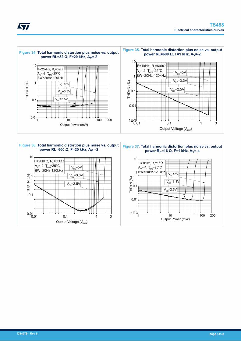
Figure 34. Total harmonic distortion plus noise vs. outputpower RL=32 Ω, F=20 kHz, AV=-2
1 10 1000.01
0.1
1
10
VCC=3.3V
VCC=5V
VCC=2.5V
F=20kHz, RL=32ΩAV=-2, TAMB=25°CBW=20Hz-120kHz
THD
+N (%
)
Output Power (mW)200
Figure 35. Total harmonic distortion plus noise vs. outputpower RL=600 Ω, F=1 kHz, AV=-2
0.01 0.1 11E-3
0.01
0.1
1
10
VCC=3.3V
VCC=5V
VCC=2.5V
F=1kHz, RL=600ΩAV=-2, TAMB=25°CBW=20Hz-120kHz
THD
+N (%
)Output Voltage (VRMS)
3
Figure 36. Total harmonic distortion plus noise vs. outputpower RL=600 Ω, F=20 kHz, AV=-2
0.01 0.1 10.01
0.1
1
10
VCC=3.3V
VCC=5V
VCC=2.5V
F=20kHz, RL=600ΩAV=-2, TAMB=25°CBW=20Hz-120kHz
THD
+N (%
)
Output Voltage (VRMS)3
Figure 37. Total harmonic distortion plus noise vs. outputpower RL=16 Ω, F=1 kHz, AV=-4
1 10 1001E-3
0.01
0.1
1
10
VCC=3.3V
VCC=5V
VCC=2.5V
F=1kHz, RL=16ΩAV=-4, TAMB=25°CBW=20Hz-120kHz
THD
+N (%
)
Output Power (mW)200
TS488Electrical characteristics curves
DS4579 - Rev 8 page 13/32
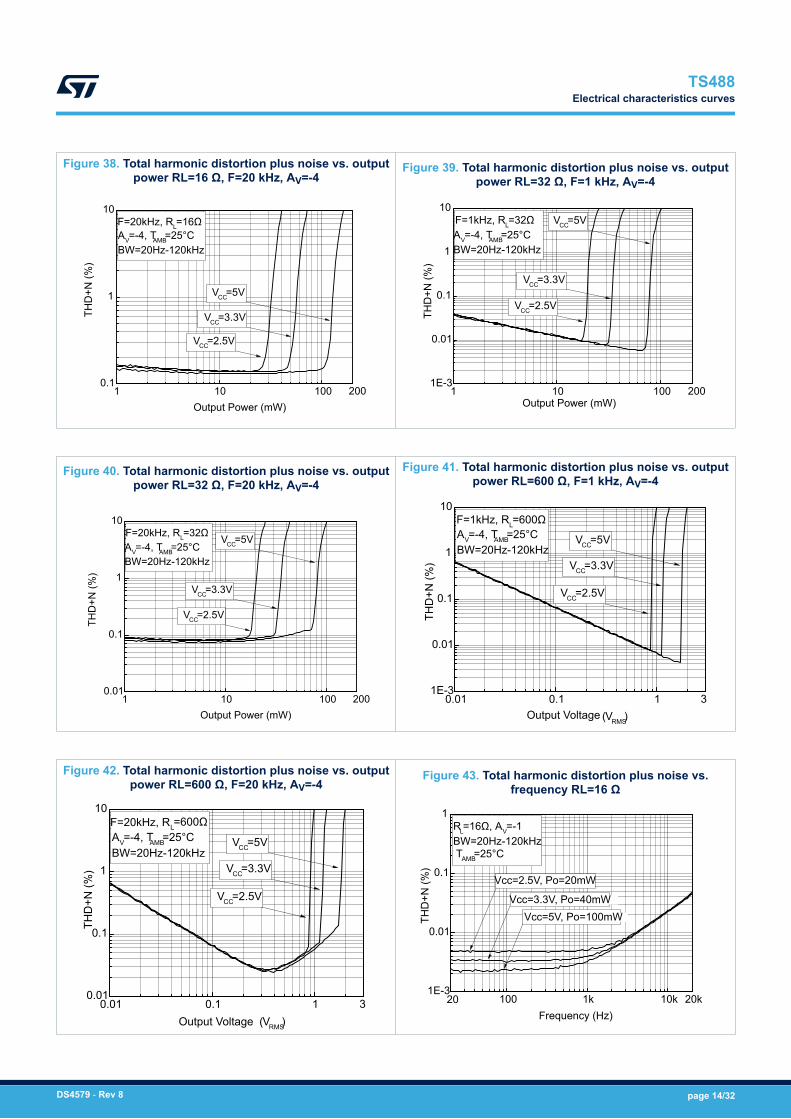
Figure 38. Total harmonic distortion plus noise vs. outputpower RL=16 Ω, F=20 kHz, AV=-4
1 10 1000.1
1
10
VCC=3.3V
VCC=5V
VCC=2.5V
F=20kHz, RL=16ΩAV=-4, TAMB=25°CBW=20Hz-120kHz
THD
+N (%
)
Output Power (mW)200
Figure 39. Total harmonic distortion plus noise vs. outputpower RL=32 Ω, F=1 kHz, AV=-4
1 10 1001E-3
0.01
0.1
1
10
VCC=3.3V
VCC=5V
VCC=2.5V
F=1kHz, RL=32ΩAV=-4, TAMB=25°CBW=20Hz-120kHz
THD
+N (%
)
Output Power (mW)200
Figure 40. Total harmonic distortion plus noise vs. outputpower RL=32 Ω, F=20 kHz, AV=-4
1 10 1000.01
0.1
1
10
VCC=3.3V
VCC=5V
VCC=2.5V
F=20kHz, RL=32ΩAV=-4, TAMB=25°CBW=20Hz-120kHz
THD
+N (%
)
Output Power (mW)200
Figure 41. Total harmonic distortion plus noise vs. outputpower RL=600 Ω, F=1 kHz, AV=-4
0.01 0.1 11E-3
0.01
0.1
1
10
VCC=3.3V
VCC=5V
VCC=2.5V
F=1kHz, RL=600ΩAV=-4, TAMB=25°CBW=20Hz-120kHz
THD
+N (%
)
Output Voltage (VRMS)3
Figure 42. Total harmonic distortion plus noise vs. outputpower RL=600 Ω, F=20 kHz, AV=-4
0.01 0.1 10.01
0.1
1
10
VCC=3.3V
VCC=5V
VCC=2.5V
F=20kHz, RL=600ΩAV=-4, TAMB=25°CBW=20Hz-120kHz
THD
+N (%
)
Output Voltage (VRMS)3
Figure 43. Total harmonic distortion plus noise vs.frequency RL=16 Ω
100 1k 10k1E-3
0.01
0.1
1
Vcc=5V, Po=100mWVcc=3.3V, Po=40mW
20k20
Vcc=2.5V, Po=20mW
RL=16Ω, AV=-1BW=20Hz-120kHzTAMB=25°C
THD
+N (%
)
Frequency (Hz)
TS488Electrical characteristics curves
DS4579 - Rev 8 page 14/32
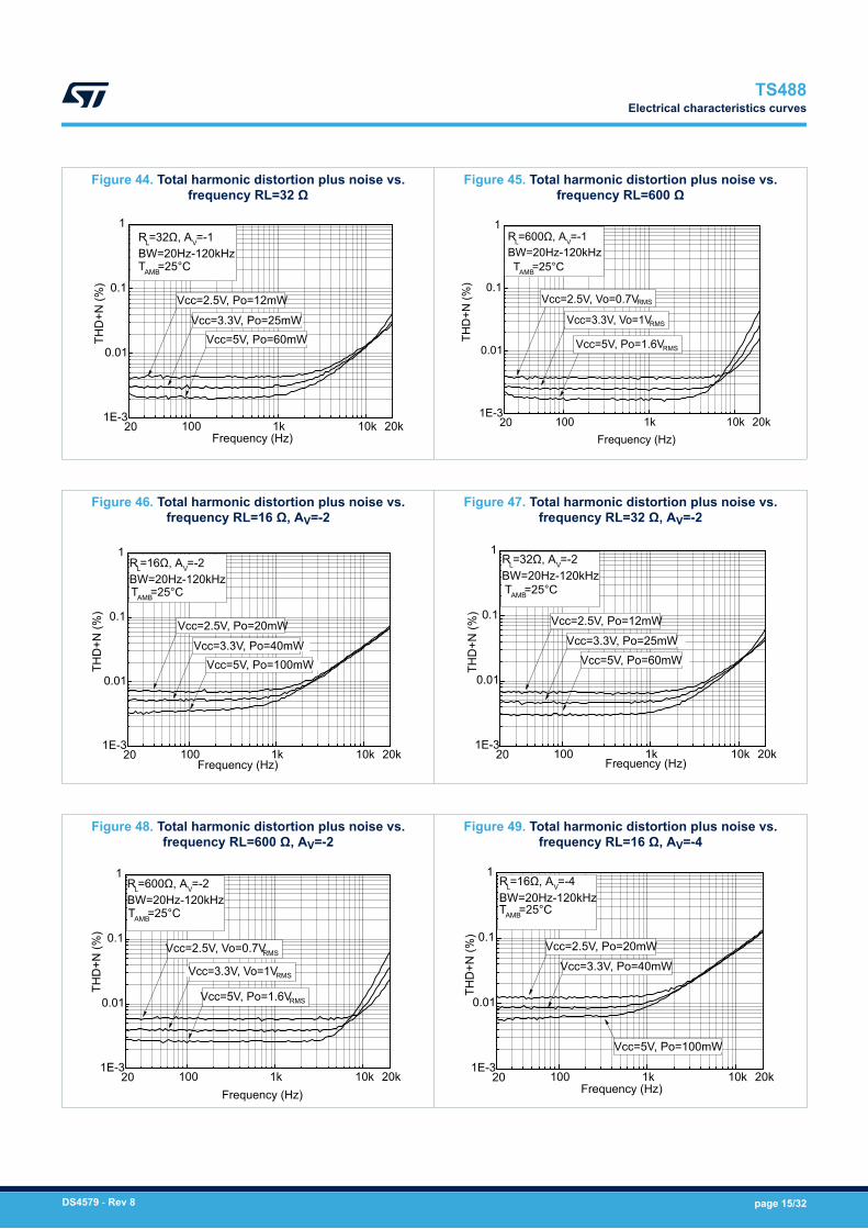
Figure 44. Total harmonic distortion plus noise vs.frequency RL=32 Ω
100 1k 10k1E-3
0.01
0.1
1
Vcc=5V, Po=60mWVcc=3.3V, Po=25mW
20k20
Vcc=2.5V, Po=12mW
RL=32Ω, AV=-1BW=20Hz-120kHzTAMB=25°C
THD
+N (%
)
Frequency (Hz)
Figure 45. Total harmonic distortion plus noise vs.frequency RL=600 Ω
100 1k 10k1E-3
0.01
0.1
1
Vcc=5V, Po=1.6VRMS
Vcc=3.3V, Vo=1VRMS
20k20
Vcc=2.5V, Vo=0.7VRMS
RL=600Ω, AV=-1BW=20Hz-120kHzTAMB=25°C
THD
+N (%
)
Frequency (Hz)
Figure 46. Total harmonic distortion plus noise vs.frequency RL=16 Ω, AV=-2
100 1k 10k1E-3
0.01
0.1
1
Vcc=5V, Po=100mWVcc=3.3V, Po=40mW
20k20
Vcc=2.5V, Po=20mW
RL=16Ω, AV=-2BW=20Hz-120kHzTAMB=25°C
THD
+N (%
)
Frequency (Hz)
Figure 47. Total harmonic distortion plus noise vs.frequency RL=32 Ω, AV=-2
100 1k 10k1E-3
0.01
0.1
1
Vcc=5V, Po=60mWVcc=3.3V, Po=25mW
20k20
Vcc=2.5V, Po=12mW
RL=32Ω, AV=-2BW=20Hz-120kHzTAMB=25°C
THD
+N (%
)
Frequency (Hz)
Figure 48. Total harmonic distortion plus noise vs.frequency RL=600 Ω, AV=-2
100 1k 10k1E-3
0.01
0.1
1
Vcc=5V, Po=1.6VRMS
Vcc=3.3V, Vo=1VRMS
20k20
Vcc=2.5V, Vo=0.7VRMS
RL=600Ω, AV=-2BW=20Hz-120kHzTAMB=25°C
THD
+N (%
)
Frequency (Hz)
Figure 49. Total harmonic distortion plus noise vs.frequency RL=16 Ω, AV=-4
100 1k 10k1E-3
0.01
0.1
1
Vcc=5V, Po=100mW
Vcc=3.3V, Po=40mW
20k20
Vcc=2.5V, Po=20mW
RL=16Ω, AV=-4BW=20Hz-120kHzTAMB=25°C
THD
+N (%
)
Frequency (Hz)
TS488Electrical characteristics curves
DS4579 - Rev 8 page 15/32
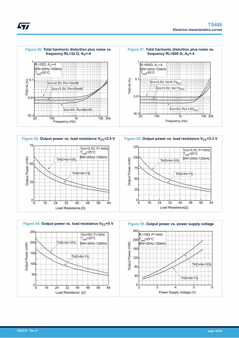
Figure 50. Total harmonic distortion plus noise vs.frequency RL=32 Ω, AV=-4
100 1k 10k1E-3
0.01
0.1
1
Vcc=5V, Po=60mW
Vcc=3.3V, Po=25mW
20k20
Vcc=2.5V, Po=12mW
RL=32Ω, AV=-4BW=20Hz-120kHzTAMB=25°C
THD
+N (%
)
Frequency (Hz)
Figure 51. Total harmonic distortion plus noise vs.frequency RL=600 Ω, AV=-4
100 1k 10k1E-3
0.01
0.1
1
Vcc=5V, Po=1.6VRMS
Vcc=3.3V, Vo=1VRMS
20k20
Vcc=2.5V, Vo=0.7VRMS
RL=600Ω, AV=-4BW=20Hz-120kHzTAMB=25°C
THD
+N (%
)
Frequency (Hz)
Figure 52. Output power vs. load resistance VCC=2.5 V
8 16 24 32 40 48 56 640
25
50
75
THD+N=10%
Vcc=2.5V, F=1kHzTAMB=25°CBW=20Hz-120kHz
Out
put P
ower
(mW
)
Load Resistance (Ω)
THD+N=1%
Figure 53. Output power vs. load resistance VCC=3.3 V
8 16 24 32 40 48 56 640
25
50
75
100
125
THD+N=10%
Vcc=3.3V, F=1kHzTAMB=25°CBW=20Hz-120kHz
Out
put P
ower
(mW
)
Load Resistance (Ω)
THD+N=1%
Figure 54. Output power vs. load resistance VCC=5 V
8 16 24 32 40 48 56 640
50
100
150
200
250
THD+N=10%
Vcc=5V, F=1kHzTAMB=25°CBW=20Hz-120kHz
Out
put P
ower
(mW
)
Load Resistance (Ω)
THD+N=1%
Figure 55. Output power vs. power supply voltage
2 3 4 5 60
40
80
120
160
200
240
THD+N=1%
RL=16Ω, F=1kHzTAMB=25°CBW=20Hz-120kHz
Out
put P
ower
(mW
)
Power Supply Voltage (V)
THD+N=10%
TS488Electrical characteristics curves
DS4579 - Rev 8 page 16/32
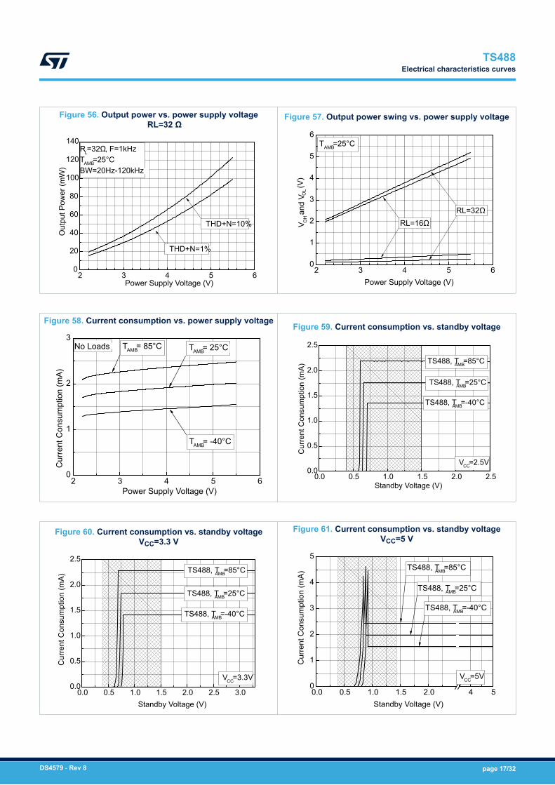
Figure 56. Output power vs. power supply voltage RL=32 Ω
2 3 4 5 60
20
40
60
80
100
120
140
THD+N=1%
RL=32Ω, F=1kHzTAMB=25°CBW=20Hz-120kHz
Out
put P
ower
(mW
)
Power Supply Voltage (V)
THD+N=10%
Figure 57. Output power swing vs. power supply voltage
2 3 4 5 60
1
2
3
4
5
6
RL=16Ω
TAMB=25°C
V OH a
nd V
OL (
V)
Power Supply Voltage (V)
RL=32Ω
Figure 58. Current consumption vs. power supply voltage
2 3 4 5 60
1
2
3
TAMB= -40°C
TAMB= 85°C TAMB= 25°CNo Loads
Cur
rent
Con
sum
ptio
n (m
A)
Power Supply Voltage (V)
Figure 59. Current consumption vs. standby voltage
0.0 0.5 1.0 1.5 2.0 2.50.0
0.5
1.0
1.5
2.0
2.5
TS488, TAMB=-40°C
TS488, TAMB=25°C
TS488, TAMB=85°C
VCC=2.5V
Cur
rent
Con
sum
ptio
n (m
A)
Standby Voltage (V)
Figure 60. Current consumption vs. standby voltageVCC=3.3 V
0.0 0.5 1.0 1.5 2.0 2.5 3.00.0
0.5
1.0
1.5
2.0
2.5
TS488, TAMB=-40°C
TS488, TAMB=25°C
TS488, TAMB=85°C
VCC=3.3V
Cur
rent
Con
sum
ptio
n (m
A)
Standby Voltage (V)
Figure 61. Current consumption vs. standby voltageVCC=5 V
0.0 0.5 1.0 1.5 2.0 4 50
1
2
3
4
5
TS488, TAMB=-40°C
TS488, TAMB=25°C
TS488, TAMB=85°C
VCC=5V
Cur
rent
Con
sum
ptio
n (m
A)
Standby Voltage (V)
TS488Electrical characteristics curves
DS4579 - Rev 8 page 17/32
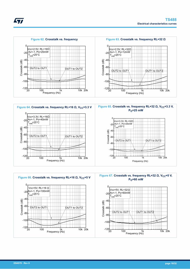
Figure 62. Crosstalk vs. frequency
100 1k 10k-120
-100
-80
-60
-40
-20
0
OUT2 to OUT1
20k20
OUT1 to OUT2
Vcc=2.5V, RL=16ΩAv=-1, Po=20mWTAMB=25°C
Cro
ssta
lk (d
B)
Frequency (Hz)
Figure 63. Crosstalk vs. frequency RL=32 Ω
100 1k 10k-120
-100
-80
-60
-40
-20
0
OUT2 to OUT1
20k20
OUT1 to OUT2
Vcc=2.5V, RL=32ΩAv=-1, Po=12mWTAMB=25°C
Cro
ssta
lk (d
B)
Frequency (Hz)
Figure 64. Crosstalk vs. frequency RL=16 Ω, VCC=3.3 V
100 1k 10k-120
-100
-80
-60
-40
-20
0
OUT2 to OUT1
20k20
OUT1 to OUT2
Vcc=3.3V, RL=16ΩAv=-1, Po=40mWTAMB=25°C
Cro
ssta
lk (d
B)
Frequency (Hz)
Figure 65. Crosstalk vs. frequency RL=32 Ω, VCC=3.3 V,PO=25 mW
100 1k 10k-120
-100
-80
-60
-40
-20
0
OUT2 to OUT1
20k20
OUT1 to OUT2
Vcc=3.3V, RL=32ΩAv=-1, Po=25mWTAMB=25°C
Cro
ssta
lk (d
B)
Frequency (Hz)
Figure 66. Crosstalk vs. frequency RL=16 Ω, VCC=5 V
100 1k 10k-120
-100
-80
-60
-40
-20
0
OUT2 to OUT1
20k20
OUT1 to OUT2
Vcc=5V, RL=16 ΩAv=-1, Po=100mWTAMB=25°C
Cro
ssta
lk (d
B)
Frequency (Hz)
Figure 67. Crosstalk vs. frequency RL=32 Ω, VCC=5 V,PO=60 mW
100 1k 10k-120
-100
-80
-60
-40
-20
0
OUT2 to OUT1
20k20
OUT1 to OUT2
Vcc=5V, RL=32ΩAv=-1, Po=60mWTAMB=25°C
Cro
ssta
lk (d
B)
Frequency (Hz)
TS488Electrical characteristics curves
DS4579 - Rev 8 page 18/32
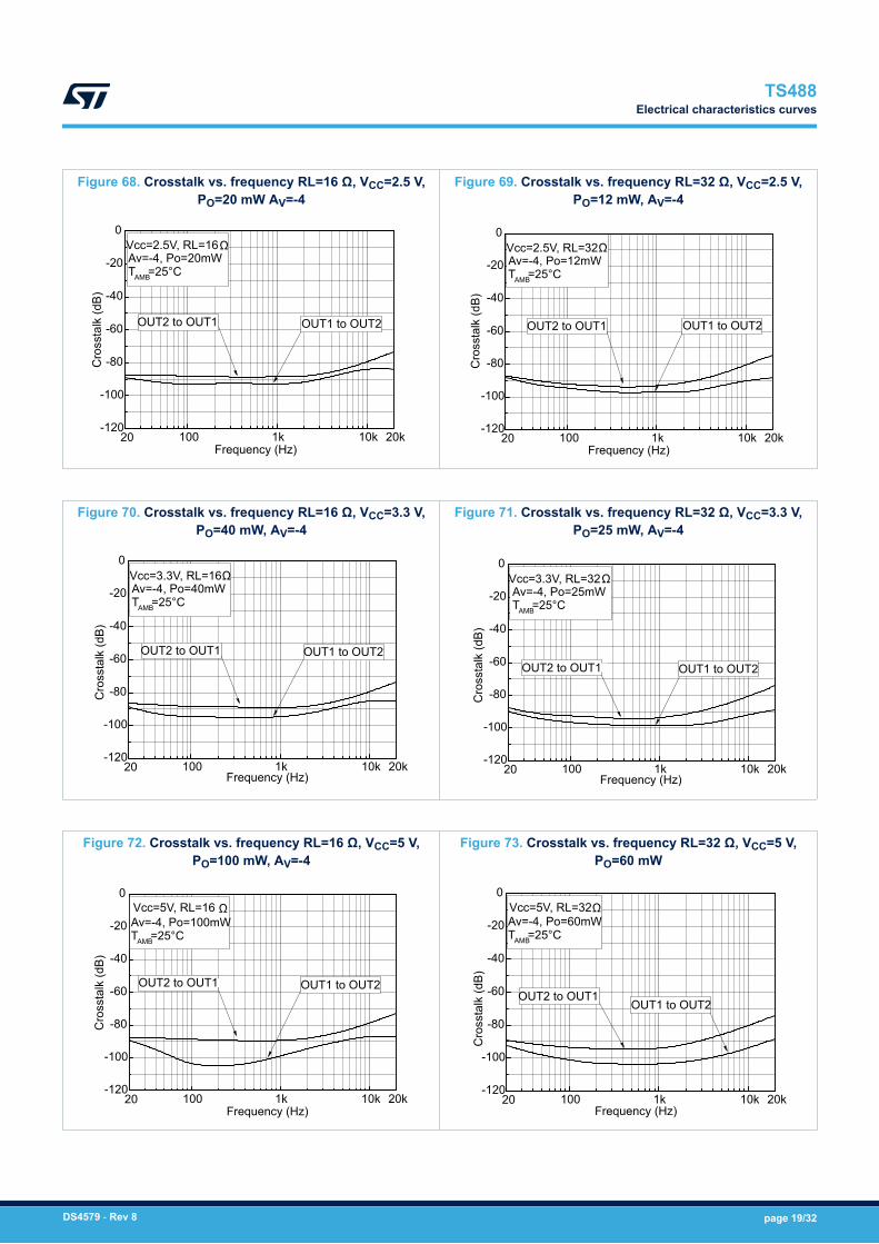
Figure 68. Crosstalk vs. frequency RL=16 Ω, VCC=2.5 V,PO=20 mW AV=-4
100 1k 10k-120
-100
-80
-60
-40
-20
0
OUT2 to OUT1
20k20
OUT1 to OUT2
Vcc=2.5V, RL=16ΩAv=-4, Po=20mWTAMB=25°C
Cro
ssta
lk (d
B)
Frequency (Hz)
Figure 69. Crosstalk vs. frequency RL=32 Ω, VCC=2.5 V,PO=12 mW, AV=-4
100 1k 10k-120
-100
-80
-60
-40
-20
0
OUT2 to OUT1
20k20
OUT1 to OUT2
Vcc=2.5V, RL=32ΩAv=-4, Po=12mWTAMB=25°C
Cro
ssta
lk (d
B)
Frequency (Hz)
Figure 70. Crosstalk vs. frequency RL=16 Ω, VCC=3.3 V,PO=40 mW, AV=-4
100 1k 10k-120
-100
-80
-60
-40
-20
0
OUT2 to OUT1
20k20
OUT1 to OUT2
Vcc=3.3V, RL=16ΩAv=-4, Po=40mWTAMB=25°C
Cro
ssta
lk (d
B)
Frequency (Hz)
Figure 71. Crosstalk vs. frequency RL=32 Ω, VCC=3.3 V,PO=25 mW, AV=-4
100 1k 10k-120
-100
-80
-60
-40
-20
0
OUT2 to OUT1
20k20
OUT1 to OUT2
Vcc=3.3V, RL=32ΩAv=-4, Po=25mWTAMB=25°C
Cro
ssta
lk (d
B)
Frequency (Hz)
Figure 72. Crosstalk vs. frequency RL=16 Ω, VCC=5 V,PO=100 mW, AV=-4
100 1k 10k-120
-100
-80
-60
-40
-20
0
OUT2 to OUT1
20k20
OUT1 to OUT2
Vcc=5V, RL=16 ΩAv=-4, Po=100mWTAMB=25°C
Cro
ssta
lk (d
B)
Frequency (Hz)
Figure 73. Crosstalk vs. frequency RL=32 Ω, VCC=5 V,PO=60 mW
100 1k 10k-120
-100
-80
-60
-40
-20
0
OUT2 to OUT1
20k20
OUT1 to OUT2
Vcc=5V, RL=32ΩAv=-4, Po=60mWTAMB=25°C
Cro
ssta
lk (d
B)
Frequency (Hz)
TS488Electrical characteristics curves
DS4579 - Rev 8 page 19/32
5 Application information
5.1 Power dissipation and efficiency
Hypotheses:• Voltage and current in the load are sinusoidal (Vout and Iout)• Supply voltage is a pure DC source (VCC)
Regarding the load, we have: VOUT = VPEAKsinωt(V) (1)
and IOUT = VOUTRL (A) (2)
and
POUT = V2PEAK2RL (A) (3)
The average current delivered by the power supply voltage is:ICCAVG = 12π∫0πVPEAKRL sin(t)dt = VPEAKπRL (A) (4)
Figure 74. Current delivered by power supply voltage in single-ended configuration
Icc (t)
TimeT/2 T
IccAVG
Vpeak/RL
0 3T/2 2T
The power delivered by power supply voltage is:Psupply = VCCICCAVG(W) (5)
So, the power dissipation by each power amplifier is:Pdiss = Psupply−POUT(W) (6)
Pdiss = 2VCCπ RL POUT − POUT(W) (7)
and the maximum value is obtained when: ∂Pdiss∂POUT = 0 (8)
and its value is:
TS488Application information
DS4579 - Rev 8 page 20/32
PdissMAX = V2CCπ2RL (W) (9)
Note: This maximum value depends only on power supply voltage and load values.The efficiency is the ratio between the output power and the power supply:η = POUTPsupply = πVpeak2VCC (10)
The maximum theoretical value is reached when Vpeak = VCC/2, soη = π4 = 78.5% (11)
5.2 Total power dissipation
The TS488 is stereo (dual channel) amplifier. It has two independent power amplifiers. Each amplifier producesheat due to its power dissipation. Therefore the maximum die temperature is the sum of each amplifier’smaximum power dissipation. It is calculated as follows:• Pdiss R = power dissipation due to the right channel power amplifier• Pdiss L = power dissipation due to the left channel power amplifier• Total Pdiss = Pdiss R + Pdiss L (W)
Typically, Pdiss R is equal to Pdiss L, giving:TotalPdiss = 2PdissR = 2PdissLTotalPdiss = 2 2VCCπ RL POUT − 2POUT (12)
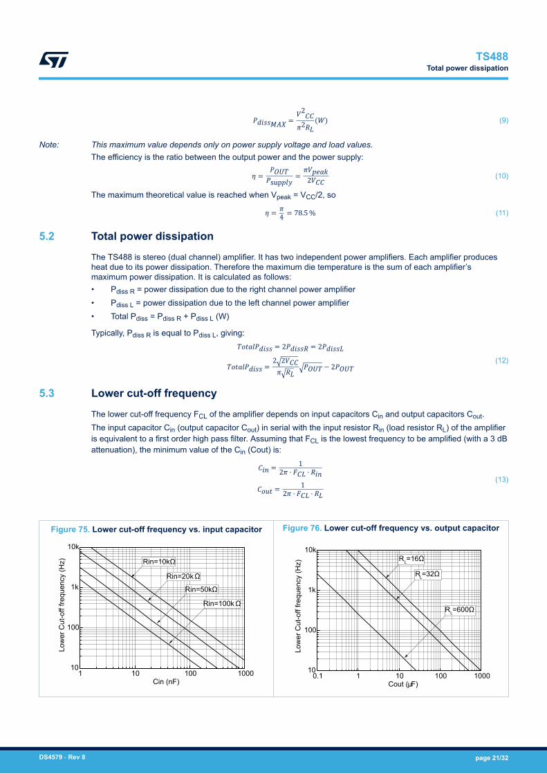
5.3 Lower cut-off frequency
The lower cut-off frequency FCL of the amplifier depends on input capacitors Cin and output capacitors Cout.The input capacitor Cin (output capacitor Cout) in serial with the input resistor Rin (load resistor RL) of the amplifieris equivalent to a first order high pass filter. Assuming that FCL is the lowest frequency to be amplified (with a 3 dBattenuation), the minimum value of the Cin (Cout) is:Cin = 12π ⋅ FCL ⋅ RinCout = 12π ⋅ FCL ⋅ RL (13)
Figure 75. Lower cut-off frequency vs. input capacitor
1 10 100 100010
100
1k
10k
Rin=50kΩ
Rin=100k Ω
Rin=20k Ω
Low
er C
ut-o
ff fre
quen
cy (H
z)
Cin (nF)
Rin=10kΩ
Figure 76. Lower cut-off frequency vs. output capacitor
0.1 1 10 100 100010
100
1k
10k
RL=32Ω
RL=600Ω
RL=16Ω
Low
er C
ut-o
ff fre
quen
cy (H
z)
Cout (μF)
TS488Total power dissipation
DS4579 - Rev 8 page 21/32
Note: In case FCL is kept the same for calculation, It must be taken in account that the 1st order high-pass filter on theinput and the 1st order high-pass filter on the output create a 2nd order high-pass filter in the audio signal pathwith an attenuation 6 dB on FCL and a roll-off 40 db⁄ decade.
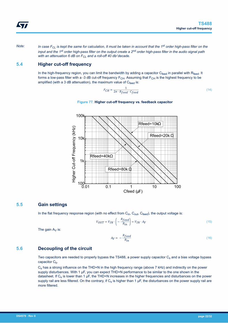
5.4 Higher cut-off frequency
In the high-frequency region, you can limit the bandwidth by adding a capacitor Cfeed in parallel with Rfeed. Itforms a low-pass filter with a -3 dB cut-off frequency FCH. Assuming that FCH is the highest frequency to beamplified (with a 3 dB attenuation), the maximum value of Cfeed is:FCH = 12π ⋅ Rfeed ⋅ Cfeed (14)
Figure 77. Higher cut-off frequency vs. feedback capacitor
0.01 0.1 1 10 100100
1k
10k
100k
Rfeed=40kΩ
Rfeed=80k Ω
Rfeed=20k Ω
Hig
her C
ut-o
ff Fr
eque
ncy
(kH
z)
Cfeed (μF)
Rfeed=10kΩ
5.5 Gain settings
In the flat frequency response region (with no effect from Cin, Cout, Cfeed), the output voltage is:VOUT = VIN ⋅ − RfeedRin = VIN ⋅ AV (15)
The gain AV is: AV = − RfeedRin (16)
5.6 Decoupling of the circuit
Two capacitors are needed to properly bypass the TS488, a power supply capacitor Cs and a bias voltage bypasscapacitor Cb.Cs has a strong influence on the THD+N in the high frequency range (above 7 kHz) and indirectly on the powersupply disturbances. With 1 µF, you can expect THD+N performance to be similar to the one shown in thedatasheet. If Cs is lower than 1 µF, the THD+N increases in the higher frequencies and disturbances on the powersupply rail are less filtered. On the contrary, if Cs is higher than 1 µF, the disturbances on the power supply rail aremore filtered.
TS488Higher cut-off frequency
DS4579 - Rev 8 page 22/32
Cb has an influence on the THD+N in the low frequency range. Its value is critical on the PSRR with groundedinputs in the lower frequencies:• If Cb is lower than 1 µF, the THD+N improves and the PSRR worsens• If Cb is higher than 1 µF, the benefit on the THD+N and PSRR is small
Note: The input capacitor Cin also has a significant effect on the PSRR at lower frequencies. The lower the value ofCin, the higher the PSRR.
5.7 Decoupling of the circuit
Two capacitors are needed to properly bypass the TS488, a power supply capacitor Cs and a bias voltage bypasscapacitor Cb.Cs has a strong influence on the THD+N in the high frequency range (above 7 kHz) and indirectly on the powersupply disturbances. With 1 µF, you can expect THD+N performance to be similar to the one shown in thedatasheet. If Cs is lower than 1 µF, the THD+N increases in the higher frequencies and disturbances on the powersupply rail are less filtered. On the contrary, if Cs is higher than 1 µF, the disturbances on the power supply rail aremore filtered.Cb has an influence on the THD+N in the low frequency range. Its value is critical on the PSRR with groundedinputs in the lower frequencies:• If Cb is lower than 1 µF, the THD+N improves and the PSRR worsens• If Cb is higher than 1 µF, the benefit on the THD+N and PSRR is small
Note: The input capacitor Cin also has a significant effect on the PSRR at lower frequencies. The lower the value ofCin, the higher the PSRR.
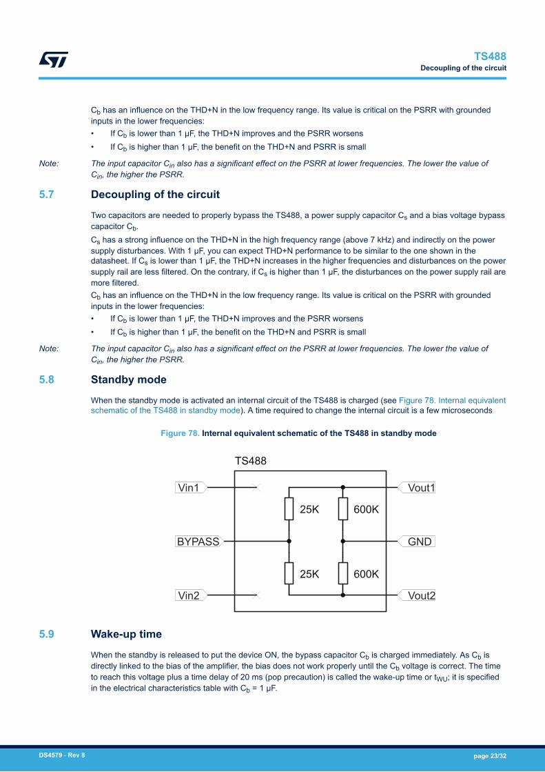
5.8 Standby mode
When the standby mode is activated an internal circuit of the TS488 is charged (see Figure 78. Internal equivalentschematic of the TS488 in standby mode). A time required to change the internal circuit is a few microseconds
Figure 78. Internal equivalent schematic of the TS488 in standby mode
25K
25K
600K
600K
Vin1
BYPASS
Vin2
Vout1
Vout2
GND
TS488
5.9 Wake-up time
When the standby is released to put the device ON, the bypass capacitor Cb is charged immediately. As Cb isdirectly linked to the bias of the amplifier, the bias does not work properly until the Cb voltage is correct. The timeto reach this voltage plus a time delay of 20 ms (pop precaution) is called the wake-up time or tWU; it is specifiedin the electrical characteristics table with Cb = 1 µF.
TS488Decoupling of the circuit
DS4579 - Rev 8 page 23/32
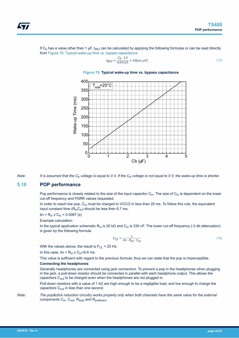
If Cb has a value other than 1 µF, tWU can be calculated by applying the following formulas or can be read directlyfrom Figure 79. Typical wake-up time vs. bypass capacitancetWU = Cb ⋅ 2.50.03125 + 20 ms; μF (17)
Figure 79. Typical wake-up time vs. bypass capacitance
0 1 2 3 4 50
50
100
150
200
250
300
350
400TAMB=25°C
Wak
e-up
Tim
e (m
s)
Cb (μF)
Note: It is assumed that the Cb voltage is equal to 0 V. If the Cb voltage is not equal to 0 V, the wake-up time is shorter.
5.10 POP performance
Pop performance is closely related to the size of the input capacitor Cin. The size of Cin is dependent on the lowercut-off frequency and PSRR values requested.In order to reach low pop, Cin must be charged to VCC/2 in less than 20 ms. To follow this rule, the equivalentinput constant time (RinCin) should be less then 6.7 ms:tin = Rin x Cin < 0.0067 (s)Example calculation:In the typical application schematic Rin is 20 kΩ and Cin is 330 nF. The lower cut-off frequency (-3 db attenuation)is given by the following formula FCL = 12π ⋅ Rin ⋅ Cin (18)
With the values above, the result is FCL = 25 Hz.In this case, tin = Rin x Cin=6.6 ms.This value is sufficient with regard to the previous formula, thus we can state that the pop is imperceptible.Connecting the headphonesGenerally headphones are connected using jack connectors. To prevent a pop in the headphones when pluggingin the jack, a pull-down resistor should be connected in parallel with each headphone output. This allows thecapacitors Cout to be charged even when the headphones are not plugged in.Pull-down resistors with a value of 1 kΩ are high enough to be a negligible load, and low enough to charge thecapacitors Cout in less than one second.
Note: The pop&click reduction circuitry works properly only when both channels have the same value for the externalcomponents Cin, Cout, Rload and Rpulldown.
TS488POP performance
DS4579 - Rev 8 page 24/32
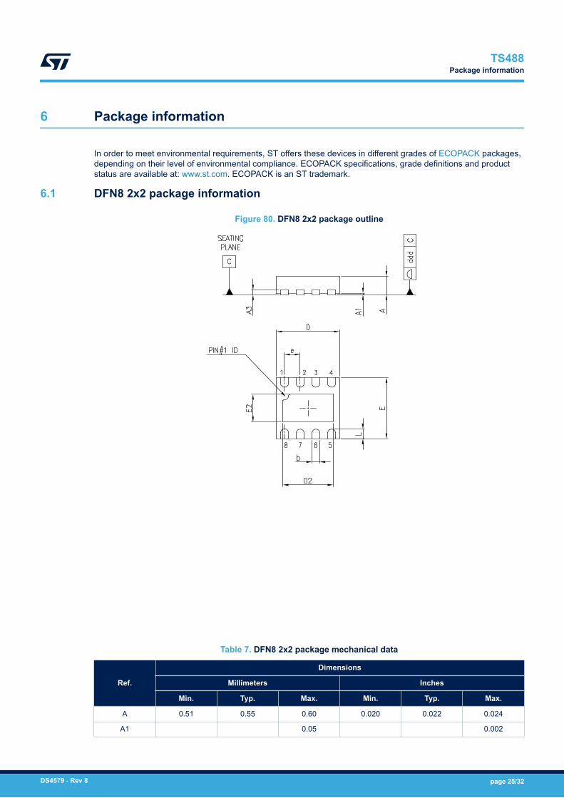
6 Package information
In order to meet environmental requirements, ST offers these devices in different grades of ECOPACK packages,depending on their level of environmental compliance. ECOPACK specifications, grade definitions and productstatus are available at: www.st.com. ECOPACK is an ST trademark.
6.1 DFN8 2x2 package information
Figure 80. DFN8 2x2 package outline
Table 7. DFN8 2x2 package mechanical data
Ref.
Dimensions
Millimeters Inches
Min. Typ. Max. Min. Typ. Max.
A 0.51 0.55 0.60 0.020 0.022 0.024
A1 0.05 0.002
TS488Package information
DS4579 - Rev 8 page 25/32
Ref.
Dimensions
Millimeters Inches
Min. Typ. Max. Min. Typ. Max.
A3 0.15 0.006
b 0.18 0.25 0.30 0.007 0.010 0.012
D 1.85 2.00 2.15 0.073 0.079 0.085
D2 1.45 1.60 1.70 0.057 0.063 0.067
E 1.85 2.00 2.15 0.073 0.079 0.085
E2 0.75 0.90 1.00 0.030 0.035 0.039
e 0.50 0.020
L 0.225 0.325 0.425 0.009 0.013 0.017
ddd 0.08 0.003
TS488DFN8 2x2 package information
DS4579 - Rev 8 page 26/32
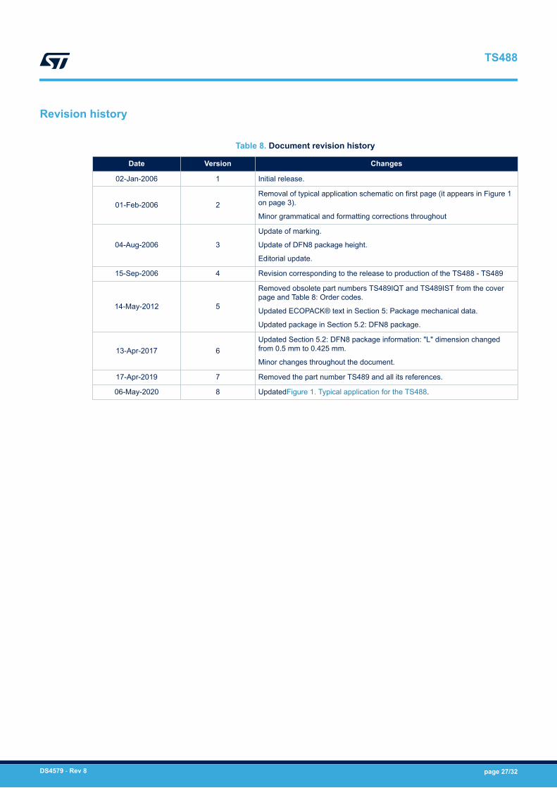
Revision history
Table 8. Document revision history
Date Version Changes
02-Jan-2006 1 Initial release.
01-Feb-2006 2Removal of typical application schematic on first page (it appears in Figure 1on page 3).
Minor grammatical and formatting corrections throughout
04-Aug-2006 3
Update of marking.
Update of DFN8 package height.
Editorial update.
15-Sep-2006 4 Revision corresponding to the release to production of the TS488 - TS489
14-May-2012 5
Removed obsolete part numbers TS489IQT and TS489IST from the coverpage and Table 8: Order codes.
Updated ECOPACK® text in Section 5: Package mechanical data.
Updated package in Section 5.2: DFN8 package.
13-Apr-2017 6Updated Section 5.2: DFN8 package information: "L" dimension changedfrom 0.5 mm to 0.425 mm.
Minor changes throughout the document.
17-Apr-2019 7 Removed the part number TS489 and all its references.
06-May-2020 8 UpdatedFigure 1. Typical application for the TS488.
TS488
DS4579 - Rev 8 page 27/32
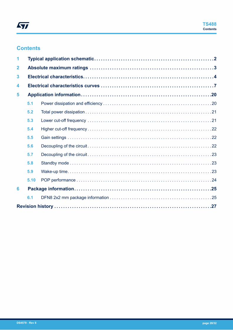
Contents
1 Typical application schematic. . . . . . . . . . . . . . . . . . . . . . . . . . . . . . . . . . . . . . . . . . . . . . . . . . . . . .2
2 Absolute maximum ratings . . . . . . . . . . . . . . . . . . . . . . . . . . . . . . . . . . . . . . . . . . . . . . . . . . . . . . . .3
3 Electrical characteristics. . . . . . . . . . . . . . . . . . . . . . . . . . . . . . . . . . . . . . . . . . . . . . . . . . . . . . . . . . .4
4 Electrical characteristics curves . . . . . . . . . . . . . . . . . . . . . . . . . . . . . . . . . . . . . . . . . . . . . . . . . . .7
5 Application information. . . . . . . . . . . . . . . . . . . . . . . . . . . . . . . . . . . . . . . . . . . . . . . . . . . . . . . . . . .20
5.1 Power dissipation and efficiency . . . . . . . . . . . . . . . . . . . . . . . . . . . . . . . . . . . . . . . . . . . . . . . . . 20
5.2 Total power dissipation . . . . . . . . . . . . . . . . . . . . . . . . . . . . . . . . . . . . . . . . . . . . . . . . . . . . . . . . . 21
5.3 Lower cut-off frequency . . . . . . . . . . . . . . . . . . . . . . . . . . . . . . . . . . . . . . . . . . . . . . . . . . . . . . . . 21
5.4 Higher cut-off frequency . . . . . . . . . . . . . . . . . . . . . . . . . . . . . . . . . . . . . . . . . . . . . . . . . . . . . . . . 22
5.5 Gain settings . . . . . . . . . . . . . . . . . . . . . . . . . . . . . . . . . . . . . . . . . . . . . . . . . . . . . . . . . . . . . . . . . 22
5.6 Decoupling of the circuit . . . . . . . . . . . . . . . . . . . . . . . . . . . . . . . . . . . . . . . . . . . . . . . . . . . . . . . . 22
5.7 Decoupling of the circuit . . . . . . . . . . . . . . . . . . . . . . . . . . . . . . . . . . . . . . . . . . . . . . . . . . . . . . . . 23
5.8 Standby mode . . . . . . . . . . . . . . . . . . . . . . . . . . . . . . . . . . . . . . . . . . . . . . . . . . . . . . . . . . . . . . . . 23
5.9 Wake-up time. . . . . . . . . . . . . . . . . . . . . . . . . . . . . . . . . . . . . . . . . . . . . . . . . . . . . . . . . . . . . . . . . 23
5.10 POP performance . . . . . . . . . . . . . . . . . . . . . . . . . . . . . . . . . . . . . . . . . . . . . . . . . . . . . . . . . . . . . 24
6 Package information. . . . . . . . . . . . . . . . . . . . . . . . . . . . . . . . . . . . . . . . . . . . . . . . . . . . . . . . . . . . . .25
6.1 DFN8 2x2 mm package information . . . . . . . . . . . . . . . . . . . . . . . . . . . . . . . . . . . . . . . . . . . . . . 25
Revision history . . . . . . . . . . . . . . . . . . . . . . . . . . . . . . . . . . . . . . . . . . . . . . . . . . . . . . . . . . . . . . . . . . . . . . .27
TS488Contents
DS4579 - Rev 8 page 28/32
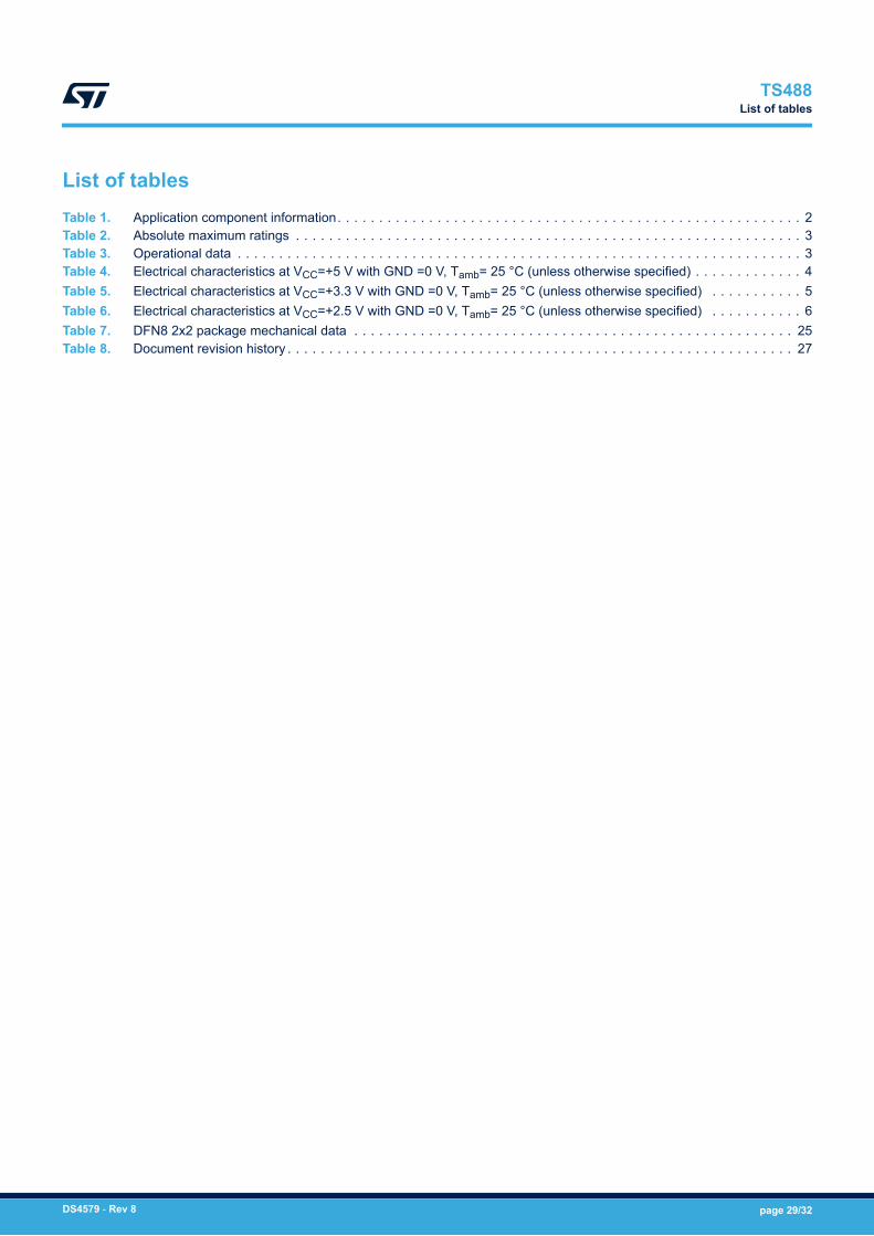
List of tablesTable 1. Application component information. . . . . . . . . . . . . . . . . . . . . . . . . . . . . . . . . . . . . . . . . . . . . . . . . . . . . . . . 2Table 2. Absolute maximum ratings . . . . . . . . . . . . . . . . . . . . . . . . . . . . . . . . . . . . . . . . . . . . . . . . . . . . . . . . . . . . . 3Table 3. Operational data . . . . . . . . . . . . . . . . . . . . . . . . . . . . . . . . . . . . . . . . . . . . . . . . . . . . . . . . . . . . . . . . . . . . 3Table 4. Electrical characteristics at VCC=+5 V with GND =0 V, Tamb= 25 °C (unless otherwise specified) . . . . . . . . . . . . . 4Table 5. Electrical characteristics at VCC=+3.3 V with GND =0 V, Tamb= 25 °C (unless otherwise specified) . . . . . . . . . . . 5Table 6. Electrical characteristics at VCC=+2.5 V with GND =0 V, Tamb= 25 °C (unless otherwise specified) . . . . . . . . . . . 6Table 7. DFN8 2x2 package mechanical data . . . . . . . . . . . . . . . . . . . . . . . . . . . . . . . . . . . . . . . . . . . . . . . . . . . . . 25Table 8. Document revision history . . . . . . . . . . . . . . . . . . . . . . . . . . . . . . . . . . . . . . . . . . . . . . . . . . . . . . . . . . . . . 27
TS488List of tables
DS4579 - Rev 8 page 29/32
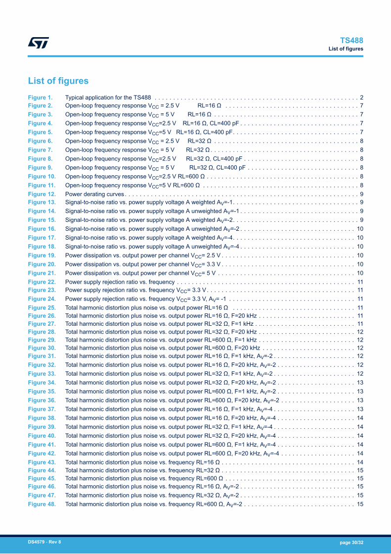
List of figuresFigure 1. Typical application for the TS488 . . . . . . . . . . . . . . . . . . . . . . . . . . . . . . . . . . . . . . . . . . . . . . . . . . . . . . . 2Figure 2. Open-loop frequency response VCC = 2.5 V RL=16 Ω . . . . . . . . . . . . . . . . . . . . . . . . . . . . . . . . . . . . 7Figure 3. Open-loop frequency response VCC = 5 V RL=16 Ω . . . . . . . . . . . . . . . . . . . . . . . . . . . . . . . . . . . . . . . 7Figure 4. Open-loop frequency response VCC=2.5 V RL=16 Ω, CL=400 pF . . . . . . . . . . . . . . . . . . . . . . . . . . . . . . . . 7Figure 5. Open-loop frequency response VCC=5 V RL=16 Ω, CL=400 pF. . . . . . . . . . . . . . . . . . . . . . . . . . . . . . . . . . 7Figure 6. Open-loop frequency response VCC = 2.5 V RL=32 Ω . . . . . . . . . . . . . . . . . . . . . . . . . . . . . . . . . . . . . . . 8Figure 7. Open-loop frequency response VCC = 5 V RL=32 Ω . . . . . . . . . . . . . . . . . . . . . . . . . . . . . . . . . . . . . . . . 8Figure 8. Open-loop frequency response VCC=2.5 V RL=32 Ω, CL=400 pF . . . . . . . . . . . . . . . . . . . . . . . . . . . . . . . 8Figure 9. Open-loop frequency response VCC = 5 V RL=32 Ω, CL=400 pF . . . . . . . . . . . . . . . . . . . . . . . . . . . . . . 8Figure 10. Open-loop frequency response VCC=2.5 V RL=600 Ω . . . . . . . . . . . . . . . . . . . . . . . . . . . . . . . . . . . . . . . . . 8Figure 11. Open-loop frequency response VCC=5 V RL=600 Ω . . . . . . . . . . . . . . . . . . . . . . . . . . . . . . . . . . . . . . . . . . 8Figure 12. Power derating curves . . . . . . . . . . . . . . . . . . . . . . . . . . . . . . . . . . . . . . . . . . . . . . . . . . . . . . . . . . . . . . . 9Figure 13. Signal-to-noise ratio vs. power supply voltage A weighted AV=-1. . . . . . . . . . . . . . . . . . . . . . . . . . . . . . . . . . 9Figure 14. Signal-to-noise ratio vs. power supply voltage A unweighted AV=-1 . . . . . . . . . . . . . . . . . . . . . . . . . . . . . . . . 9Figure 15. Signal-to-noise ratio vs. power supply voltage A weighted AV=-2. . . . . . . . . . . . . . . . . . . . . . . . . . . . . . . . . . 9Figure 16. Signal-to-noise ratio vs. power supply voltage A unweighted AV=-2 . . . . . . . . . . . . . . . . . . . . . . . . . . . . . . . 10Figure 17. Signal-to-noise ratio vs. power supply voltage A weighted AV=-4. . . . . . . . . . . . . . . . . . . . . . . . . . . . . . . . . 10Figure 18. Signal-to-noise ratio vs. power supply voltage A unweighted AV=-4 . . . . . . . . . . . . . . . . . . . . . . . . . . . . . . . 10Figure 19. Power dissipation vs. output power per channel VCC= 2.5 V . . . . . . . . . . . . . . . . . . . . . . . . . . . . . . . . . . . . 10Figure 20. Power dissipation vs. output power per channel VCC= 3.3 V . . . . . . . . . . . . . . . . . . . . . . . . . . . . . . . . . . . . 10Figure 21. Power dissipation vs. output power per channel VCC= 5 V . . . . . . . . . . . . . . . . . . . . . . . . . . . . . . . . . . . . . 10Figure 22. Power supply rejection ratio vs. frequency . . . . . . . . . . . . . . . . . . . . . . . . . . . . . . . . . . . . . . . . . . . . . . . . 11Figure 23. Power supply rejection ratio vs. frequency VCC= 3.3 V . . . . . . . . . . . . . . . . . . . . . . . . . . . . . . . . . . . . . . . . 11Figure 24. Power supply rejection ratio vs. frequency VCC= 3.3 V, AV= -1 . . . . . . . . . . . . . . . . . . . . . . . . . . . . . . . . . . 11Figure 25. Total harmonic distortion plus noise vs. output power RL=16 Ω . . . . . . . . . . . . . . . . . . . . . . . . . . . . . . . . . 11Figure 26. Total harmonic distortion plus noise vs. output power RL=16 Ω, F=20 kHz . . . . . . . . . . . . . . . . . . . . . . . . . . 11Figure 27. Total harmonic distortion plus noise vs. output power RL=32 Ω, F=1 kHz . . . . . . . . . . . . . . . . . . . . . . . . . . . 11Figure 28. Total harmonic distortion plus noise vs. output power RL=32 Ω, F=20 kHz . . . . . . . . . . . . . . . . . . . . . . . . . . 12Figure 29. Total harmonic distortion plus noise vs. output power RL=600 Ω, F=1 kHz . . . . . . . . . . . . . . . . . . . . . . . . . . 12Figure 30. Total harmonic distortion plus noise vs. output power RL=600 Ω, F=20 kHz . . . . . . . . . . . . . . . . . . . . . . . . . 12Figure 31. Total harmonic distortion plus noise vs. output power RL=16 Ω, F=1 kHz, AV=-2 . . . . . . . . . . . . . . . . . . . . . . 12Figure 32. Total harmonic distortion plus noise vs. output power RL=16 Ω, F=20 kHz, AV=-2 . . . . . . . . . . . . . . . . . . . . . 12Figure 33. Total harmonic distortion plus noise vs. output power RL=32 Ω, F=1 kHz, AV=-2 . . . . . . . . . . . . . . . . . . . . . . 12Figure 34. Total harmonic distortion plus noise vs. output power RL=32 Ω, F=20 kHz, AV=-2 . . . . . . . . . . . . . . . . . . . . . 13Figure 35. Total harmonic distortion plus noise vs. output power RL=600 Ω, F=1 kHz, AV=-2 . . . . . . . . . . . . . . . . . . . . . 13Figure 36. Total harmonic distortion plus noise vs. output power RL=600 Ω, F=20 kHz, AV=-2 . . . . . . . . . . . . . . . . . . . . 13Figure 37. Total harmonic distortion plus noise vs. output power RL=16 Ω, F=1 kHz, AV=-4 . . . . . . . . . . . . . . . . . . . . . . 13Figure 38. Total harmonic distortion plus noise vs. output power RL=16 Ω, F=20 kHz, AV=-4 . . . . . . . . . . . . . . . . . . . . . 14Figure 39. Total harmonic distortion plus noise vs. output power RL=32 Ω, F=1 kHz, AV=-4 . . . . . . . . . . . . . . . . . . . . . . 14Figure 40. Total harmonic distortion plus noise vs. output power RL=32 Ω, F=20 kHz, AV=-4 . . . . . . . . . . . . . . . . . . . . . 14Figure 41. Total harmonic distortion plus noise vs. output power RL=600 Ω, F=1 kHz, AV=-4 . . . . . . . . . . . . . . . . . . . . . 14Figure 42. Total harmonic distortion plus noise vs. output power RL=600 Ω, F=20 kHz, AV=-4 . . . . . . . . . . . . . . . . . . . . 14Figure 43. Total harmonic distortion plus noise vs. frequency RL=16 Ω . . . . . . . . . . . . . . . . . . . . . . . . . . . . . . . . . . . . 14Figure 44. Total harmonic distortion plus noise vs. frequency RL=32 Ω . . . . . . . . . . . . . . . . . . . . . . . . . . . . . . . . . . . . 15Figure 45. Total harmonic distortion plus noise vs. frequency RL=600 Ω . . . . . . . . . . . . . . . . . . . . . . . . . . . . . . . . . . . 15Figure 46. Total harmonic distortion plus noise vs. frequency RL=16 Ω, AV=-2 . . . . . . . . . . . . . . . . . . . . . . . . . . . . . . . 15Figure 47. Total harmonic distortion plus noise vs. frequency RL=32 Ω, AV=-2 . . . . . . . . . . . . . . . . . . . . . . . . . . . . . . . 15Figure 48. Total harmonic distortion plus noise vs. frequency RL=600 Ω, AV=-2 . . . . . . . . . . . . . . . . . . . . . . . . . . . . . . 15
TS488List of figures
DS4579 - Rev 8 page 30/32
Figure 49. Total harmonic distortion plus noise vs. frequency RL=16 Ω, AV=-4 . . . . . . . . . . . . . . . . . . . . . . . . . . . . . . . 15Figure 50. Total harmonic distortion plus noise vs. frequency RL=32 Ω, AV=-4 . . . . . . . . . . . . . . . . . . . . . . . . . . . . . . . 16Figure 51. Total harmonic distortion plus noise vs. frequency RL=600 Ω, AV=-4 . . . . . . . . . . . . . . . . . . . . . . . . . . . . . . 16Figure 52. Output power vs. load resistance VCC=2.5 V . . . . . . . . . . . . . . . . . . . . . . . . . . . . . . . . . . . . . . . . . . . . . . 16Figure 53. Output power vs. load resistance VCC=3.3 V . . . . . . . . . . . . . . . . . . . . . . . . . . . . . . . . . . . . . . . . . . . . . . 16Figure 54. Output power vs. load resistance VCC=5 V . . . . . . . . . . . . . . . . . . . . . . . . . . . . . . . . . . . . . . . . . . . . . . . . 16Figure 55. Output power vs. power supply voltage . . . . . . . . . . . . . . . . . . . . . . . . . . . . . . . . . . . . . . . . . . . . . . . . . . 16Figure 56. Output power vs. power supply voltage RL=32 Ω . . . . . . . . . . . . . . . . . . . . . . . . . . . . . . . . . . . . . . . . . 17Figure 57. Output power swing vs. power supply voltage. . . . . . . . . . . . . . . . . . . . . . . . . . . . . . . . . . . . . . . . . . . . . . 17Figure 58. Current consumption vs. power supply voltage . . . . . . . . . . . . . . . . . . . . . . . . . . . . . . . . . . . . . . . . . . . . . 17Figure 59. Current consumption vs. standby voltage . . . . . . . . . . . . . . . . . . . . . . . . . . . . . . . . . . . . . . . . . . . . . . . . . 17Figure 60. Current consumption vs. standby voltage VCC=3.3 V . . . . . . . . . . . . . . . . . . . . . . . . . . . . . . . . . . . . . . . . . 17Figure 61. Current consumption vs. standby voltage VCC=5 V . . . . . . . . . . . . . . . . . . . . . . . . . . . . . . . . . . . . . . . . . . 17Figure 62. Crosstalk vs. frequency . . . . . . . . . . . . . . . . . . . . . . . . . . . . . . . . . . . . . . . . . . . . . . . . . . . . . . . . . . . . . 18Figure 63. Crosstalk vs. frequency RL=32 Ω . . . . . . . . . . . . . . . . . . . . . . . . . . . . . . . . . . . . . . . . . . . . . . . . . . . . . . 18Figure 64. Crosstalk vs. frequency RL=16 Ω, VCC=3.3 V . . . . . . . . . . . . . . . . . . . . . . . . . . . . . . . . . . . . . . . . . . . . . . 18Figure 65. Crosstalk vs. frequency RL=32 Ω, VCC=3.3 V, PO=25 mW . . . . . . . . . . . . . . . . . . . . . . . . . . . . . . . . . . . . . 18Figure 66. Crosstalk vs. frequency RL=16 Ω, VCC=5 V . . . . . . . . . . . . . . . . . . . . . . . . . . . . . . . . . . . . . . . . . . . . . . . 18Figure 67. Crosstalk vs. frequency RL=32 Ω, VCC=5 V, PO=60 mW . . . . . . . . . . . . . . . . . . . . . . . . . . . . . . . . . . . . . . 18Figure 68. Crosstalk vs. frequency RL=16 Ω, VCC=2.5 V, PO=20 mW AV=-4 . . . . . . . . . . . . . . . . . . . . . . . . . . . . . . . . 19Figure 69. Crosstalk vs. frequency RL=32 Ω, VCC=2.5 V, PO=12 mW, AV=-4 . . . . . . . . . . . . . . . . . . . . . . . . . . . . . . . . 19Figure 70. Crosstalk vs. frequency RL=16 Ω, VCC=3.3 V, PO=40 mW, AV=-4 . . . . . . . . . . . . . . . . . . . . . . . . . . . . . . . . 19Figure 71. Crosstalk vs. frequency RL=32 Ω, VCC=3.3 V, PO=25 mW, AV=-4 . . . . . . . . . . . . . . . . . . . . . . . . . . . . . . . . 19Figure 72. Crosstalk vs. frequency RL=16 Ω, VCC=5 V, PO=100 mW, AV=-4 . . . . . . . . . . . . . . . . . . . . . . . . . . . . . . . . 19Figure 73. Crosstalk vs. frequency RL=32 Ω, VCC=5 V, PO=60 mW . . . . . . . . . . . . . . . . . . . . . . . . . . . . . . . . . . . . . . 19Figure 74. Current delivered by power supply voltage in single-ended configuration . . . . . . . . . . . . . . . . . . . . . . . . . . . 20Figure 75. Lower cut-off frequency vs. input capacitor . . . . . . . . . . . . . . . . . . . . . . . . . . . . . . . . . . . . . . . . . . . . . . . 21Figure 76. Lower cut-off frequency vs. output capacitor . . . . . . . . . . . . . . . . . . . . . . . . . . . . . . . . . . . . . . . . . . . . . . 21Figure 77. Higher cut-off frequency vs. feedback capacitor . . . . . . . . . . . . . . . . . . . . . . . . . . . . . . . . . . . . . . . . . . . . 22Figure 78. Internal equivalent schematic of the TS488 in standby mode . . . . . . . . . . . . . . . . . . . . . . . . . . . . . . . . . . . 23Figure 79. Typical wake-up time vs. bypass capacitance . . . . . . . . . . . . . . . . . . . . . . . . . . . . . . . . . . . . . . . . . . . . . . 24Figure 80. DFN8 2x2 package outline . . . . . . . . . . . . . . . . . . . . . . . . . . . . . . . . . . . . . . . . . . . . . . . . . . . . . . . . . . . 25
TS488List of figures
DS4579 - Rev 8 page 31/32
IMPORTANT NOTICE – PLEASE READ CAREFULLY
STMicroelectronics NV and its subsidiaries (“ST”) reserve the right to make changes, corrections, enhancements, modifications, and improvements to STproducts and/or to this document at any time without notice. Purchasers should obtain the latest relevant information on ST products before placing orders. STproducts are sold pursuant to ST’s terms and conditions of sale in place at the time of order acknowledgement.
Purchasers are solely responsible for the choice, selection, and use of ST products and ST assumes no liability for application assistance or the design ofPurchasers’ products.
No license, express or implied, to any intellectual property right is granted by ST herein.
Resale of ST products with provisions different from the information set forth herein shall void any warranty granted by ST for such product.
ST and the ST logo are trademarks of ST. For additional information about ST trademarks, please refer to www.st.com/trademarks. All other product or servicenames are the property of their respective owners.
Information in this document supersedes and replaces information previously supplied in any prior versions of this document.
© 2020 STMicroelectronics – All rights reserved
TS488
DS4579 - Rev 8 page 32/32