
Datasheet - STH13N120K5-2AG - Automotive-grade N-channel ... · 1 Electrical ratings Table 1....
16
1 2 TAB 3 H 2 PAK-2 D(TAB) G(1) S(2,3) NCHG1DTABS23TZ Features Order code V DS R DS(on) max. I D P TOT STH13N120K5-2AG 1200 V 0.69 Ω 12 A 250 W • AEC-Q101 qualified • Industry’s lowest R DS(on) x area • Industry’s best FoM (figure of merit) • Ultra-low gate charge • 100% avalanche tested • Zener-protected Applications • Switching applications Description This very high voltage N-channel Power MOSFET is designed using MDmesh K5 technology based on an innovative proprietary vertical structure. The result is a dramatic reduction in on-resistance and ultra-low gate charge for applications requiring superior power density and high efficiency. Product status link STH13N120K5-2AG Product summary Order code STH13N120K5-2AG Marking 13N120K5 Package H²PAK-2 Packing Tape and reel Automotive-grade N-channel 1200 V, 0.62 Ω typ., 12 A, MDmesh K5 Power MOSFET in an H²PAK‑2 package STH13N120K5-2AG Datasheet DS12917 - Rev 3 - October 2019 For further information contact your local STMicroelectronics sales office. www.st.com
Transcript of Datasheet - STH13N120K5-2AG - Automotive-grade N-channel ... · 1 Electrical ratings Table 1....
1
2
TAB
3
H2PAK-2
D(TAB)
G(1)
S(2,3)NCHG1DTABS23TZ
FeaturesOrder code VDS RDS(on) max. ID PTOT
STH13N120K5-2AG 1200 V 0.69 Ω 12 A 250 W
• AEC-Q101 qualified • Industry’s lowest RDS(on) x area• Industry’s best FoM (figure of merit)• Ultra-low gate charge• 100% avalanche tested• Zener-protected
Applications• Switching applications
DescriptionThis very high voltage N-channel Power MOSFET is designed using MDmesh K5technology based on an innovative proprietary vertical structure. The result is adramatic reduction in on-resistance and ultra-low gate charge for applicationsrequiring superior power density and high efficiency.
Product status link
STH13N120K5-2AG
Product summary
Order code STH13N120K5-2AG
Marking 13N120K5
Package H²PAK-2
Packing Tape and reel
Automotive-grade N-channel 1200 V, 0.62 Ω typ., 12 A, MDmesh K5 Power MOSFET in an H²PAK‑2 package
STH13N120K5-2AG
Datasheet
DS12917 - Rev 3 - October 2019For further information contact your local STMicroelectronics sales office.
www.st.com
1 Electrical ratings
Table 1. Absolute maximum ratings
Symbol Parameter Value Unit
VGS Gate-source voltage ±30 V
IDDrain current at TC = 25 °C 12 A
Drain current at TC = 100 °C 7.6 A
IDM (1) Drain current (pulsed) 48 A
PTOT Total power dissipation at TC = 25 °C 250 W
IAR (2) Maximum current during repetitive or single-pulse avalanche 4 A
EAS (3) Single-pulse avalanche energy 215 mJ
dv/dt (4) Peak diode recovery voltage slope 4.5 V/ns
dv/dt(5) MOSFET dv/dt ruggedness 50 V/ns
Tj Operating junction temperature range-55 to 150 °C
Tstg Storage temperature range
1. Pulse width limited by safe operating area.2. Pulse width limited by TJmax.
3. Starting TJ = 25 °C, ID=IAR, VDD= 50 V
4. ISD ≤ 12 A, di/dt ≤ 100 A/µs, VDS (peak) ≤ V(BR)DSS
5. VDS ≤ 960 V
Table 2. Thermal data
Symbol Parameter Value Unit
Rthj-case Thermal resistance junction-case 0.5 °C/W
Rthj-pcb (1) Thermal resistance junction-pcb 30 °C/W
1. When mounted on FR-4 board of 1 inch², 2oz Cu.
STH13N120K5-2AGElectrical ratings
DS12917 - Rev 3 page 2/16
2 Electrical characteristics
(TCASE = 25 °C unless otherwise specified)
Table 3. On/off states
Symbol Parameter Test conditions Min. Typ. Max. Unit
V(BR)DSS Drain-source breakdown voltage VGS = 0 V, ID = 1 mA 1200 V
IDSS Zero gate voltage drain current
VGS = 0 V, VDS = 1200 V 1 µA
VGS = 0 V, VDS = 1200 V,
Tc = 125 °C (1)50 µA
IGSS Gate body leakage current VDS = 0 V, VGS = ±20 V ±10 µA
VGS(th) Gate threshold voltage VDS = VGS, ID = 100 µA 3 4 5 V
RDS(on) Static drain-source on- resistance VGS = 10 V, ID= 6 A 0.62 0.69 Ω
1. Defined by design, not subject to production test.
Table 4. Dynamic
Symbol Parameter Test conditions Min. Typ. Max. Unit
Ciss Input capacitanceVGS = 0 V, VDS = 100 V,
f = 1 MHz
- 1370 - pF
Coss Output capacitance - 110 - pF
Crss Reverse transfer capacitance - 0.6 - pF
Co(tr)(1) Time-related equivalentcapacitance
VGS = 0 V, VDS = 0 to 960 V- 128 - pF
Co(er)(2) Energy-related equivalentcapacitance - 42 - pF
RG Intrinsic gate resistance f = 1 MHz, ID = 0 A - 3 - Ω
Qg Total gate charge VDD = 960 V, ID = 12 A
VGS = 0 to 10 V
(see Figure 15. Test circuit for gatecharge behavior)
- 44.2 - nC
Qgs Gate-source charge - 7.3 - nC
Qgd Gate-drain charge - 30 - nC
1. Time-related is defined as a constant equivalent capacitance giving the same charging time as Coss when VDS increasesfrom 0 to 80% VDSS.
2. Energy-related is defined as a constant equivalent capacitance giving the same stored energy as Coss when VDS increasesfrom 0 to 80% VDSS .
Table 5. Switching times
Symbol Parameter Test conditions Min. Typ. Max. Unit
td(on) Turn-on delay time VDD = 600 V, ID = 6 A,
RG = 4.7 Ω, VGS = 10 V
(see Figure 14. Test circuit forresistive load switching times andFigure 19. Switching timewaveform)
- 23 - ns
tr Rise time - 11 - ns
td(off) Turn-off delay time - 68.5 - ns
tf Fall time - 18.5 - ns
STH13N120K5-2AGElectrical characteristics
DS12917 - Rev 3 page 3/16
Table 6. Source-drain diode
Symbol Parameter Test conditions Min. Typ. Max. Unit
ISD Source-drain current - 12 A
ISDM Source-drain current (pulsed) - 48 A
VSD(1) Forward on voltage ISD = 12 A, VGS = 0 V - 1.5 V
trr Reverse recovery time ISD = 12 A, VDD = 60 V
di/dt = 100 A/µs,
(see Figure 16. Test circuit forinductive load switching and dioderecovery times)
- 630 ns
Qrr Reverse recovery charge - 12.6 µC
IRRM Reverse recovery current - 40 A
trr Reverse recovery time ISD = 12 A,VDD = 60 V
di/dt = 100 A/µs, Tj = 150 °C
(see Figure 16. Test circuit forinductive load switching and dioderecovery times)
- 892 ns
Qrr Reverse recovery charge - 15.6 µC
IRRM Reverse recovery current - 35 A
1. Pulsed: pulse duration = 300µs, duty cycle 1.5%
Table 7. Gate-source Zener diode
Symbol Parameter Test conditions Min Typ. Max. Unit
V(BR)GSO Gate-source breakdown voltage IGS = ±1 mA, ID = 0 A 30 - V
The built-in back-to-back Zener diodes have been specifically designed to enhance the ESD capability of thedevice. The Zener voltage is appropriate for efficient and cost-effective intervention to protect the device integrity.These integrated Zener diodes thus eliminate the need for external components.
STH13N120K5-2AGElectrical characteristics
DS12917 - Rev 3 page 4/16
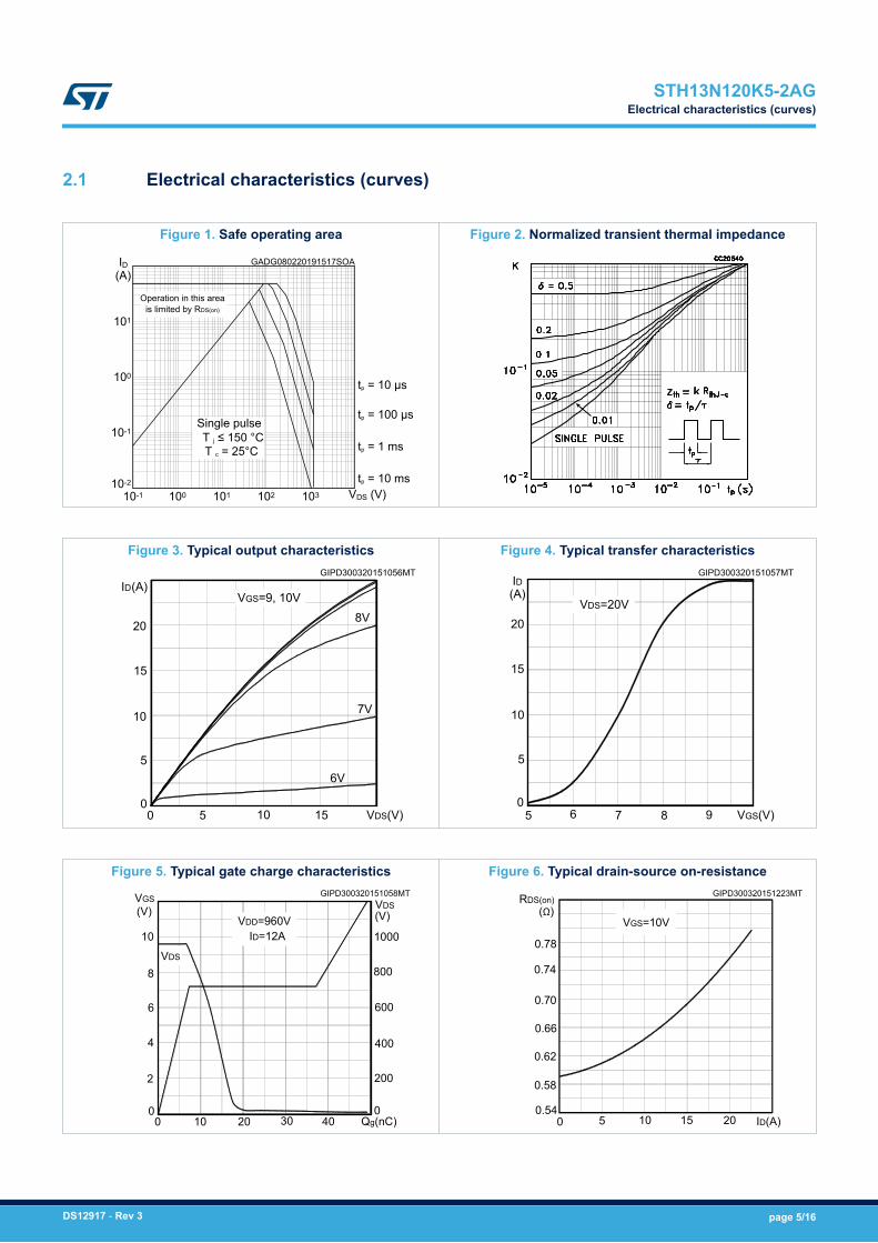
2.1 Electrical characteristics (curves)
Figure 1. Safe operating area
GADG080220191517SOA
101
100
10-1
10-2
10-1 100 101 102 103
ID (A)
VDS (V)
Operation in this areais limited by RDS(on)
tp = 10 μs
tp = 1 ms
tp = 10 ms
tp = 100 μs
T j ≤ 150 °CT c = 25°C
Single pulse
Figure 2. Normalized transient thermal impedance
Figure 3. Typical output characteristics
ID
15
5
00 5 VDS(V)10
(A)
15
6V
7V
VGS=9, 10V
10
208V
GIPD300320151056MT
Figure 4. Typical transfer characteristics
ID
20
10
05 7 VGS(V)9
(A)
6 8
5
15
VDS=20V
GIPD300320151057MT
Figure 5. Typical gate charge characteristics
VGS
6
4
2
00 20 Qg(nC)
(V)
8
30 40
10VDD=960V
ID=12A
600
400
200
0
800
1000VDS
10
VDS(V)
GIPD300320151058MT
Figure 6. Typical drain-source on-resistanceGIPD300320151223MTRDS(on)
0.62
0.58
0.540 10 ID(A)
(Ω)
5 15
0.66
VGS=10V
0.7
0.74
0.78
20
0
STH13N120K5-2AGElectrical characteristics (curves)
DS12917 - Rev 3 page 5/16
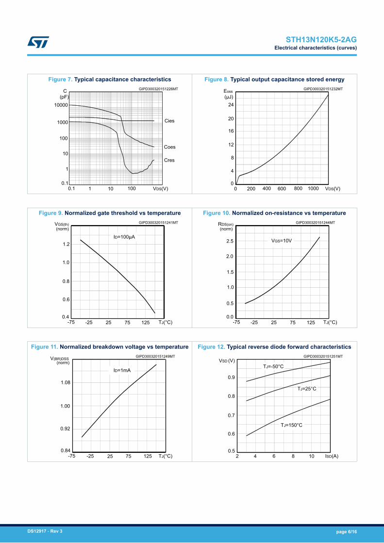
Figure 7. Typical capacitance characteristics
C
100
10
1
0.10.1 10 VDS(V)
(pF)
1 100
Cies
Coes
Cres
1000
10000
GIPD300320151226MT
Figure 8. Typical output capacitance stored energy
Eoss
8
4
00 200 VDS(V)
(µJ)
800400 600
12
1000
16
20
24
GIPD300320151232MT
Figure 9. Normalized gate threshold vs temperature
VGS(th)
1.0
0.8
0.6
0.4-75 TJ(°C)
(norm)
-25
1.2
25 75
ID=100µA
125
GIPD300320151241MT
Figure 10. Normalized on-resistance vs temperature
1.5
1.0
0.5
0.0TJ(°C)
2.0
2.5
RDS(on)(norm)
VGS=10V
-75 -25 25 75 125
GIPD300320151244MT
Figure 11. Normalized breakdown voltage vs temperature
V(BR)DSS
-75 TJ(°C)
(norm)
-25 7525 1250.84
0.92
1.00
1.08
ID=1mA
GIPD300320151249MT
Figure 12. Typical reverse diode forward characteristics
VSD
4 ISD(A)
(V)
2 106 80.5
0.6
0.7
0.8
TJ=-50°C
TJ=150°C
TJ=25°C
0.9
GIPD300320151251MT
STH13N120K5-2AGElectrical characteristics (curves)
DS12917 - Rev 3 page 6/16
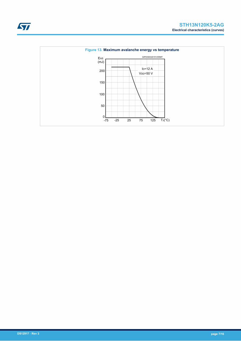
Figure 13. Maximum avalanche energy vs temperature
EAS
-75 25 TJ(°C)
(mJ)
-25 75 1250
50
100
150
200 ID=12 AVDD=50 V
GIPD300320151255MT
STH13N120K5-2AGElectrical characteristics (curves)
DS12917 - Rev 3 page 7/16
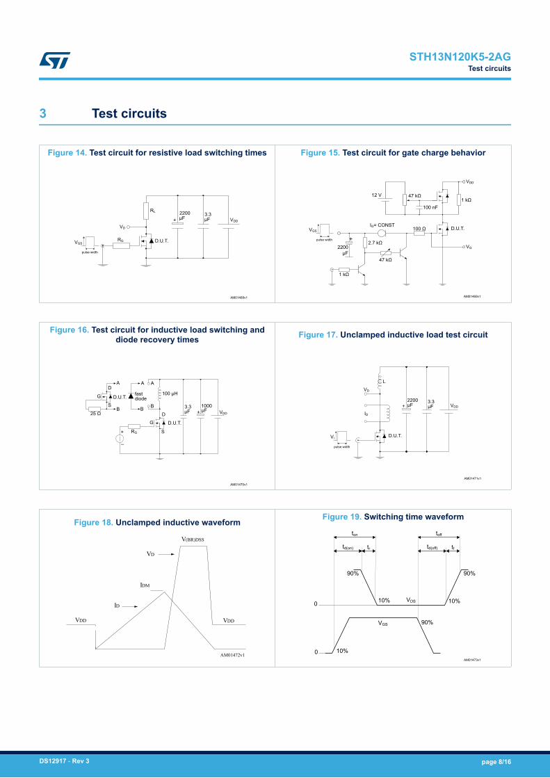
3 Test circuits
Figure 14. Test circuit for resistive load switching times
AM01468v1
VD
RG
RL
D.U.T.
2200μF VDD
3.3μF+
pulse width
VGS
Figure 15. Test circuit for gate charge behavior
AM01469v1
47 kΩ1 kΩ
47 kΩ
2.7 kΩ
1 kΩ
12 V
IG= CONST100 Ω
100 nF
D.U.T.
+pulse width
VGS
2200μF
VG
VDD
Figure 16. Test circuit for inductive load switching anddiode recovery times
AM01470v1
AD
D.U.T.S
B
G
25 Ω
A A
B B
RG
GD
S
100 µH
µF3.3 1000
µF VDD
D.U.T.
+
_
+
fastdiode
Figure 17. Unclamped inductive load test circuit
AM01471v1
VD
ID
D.U.T.
L
VDD+
pulse width
Vi
3.3µF
2200µF
Figure 18. Unclamped inductive waveform
AM01472v1
V(BR)DSS
VDDVDD
VD
IDM
ID
Figure 19. Switching time waveform
AM01473v1
0
VGS 90%
VDS
90%
10%
90%
10%
10%
ton
td(on) tr
0
toff
td(off) tf
STH13N120K5-2AGTest circuits
DS12917 - Rev 3 page 8/16
4 Package information
In order to meet environmental requirements, ST offers these devices in different grades of ECOPACK packages,depending on their level of environmental compliance. ECOPACK specifications, grade definitions and productstatus are available at: www.st.com. ECOPACK is an ST trademark.
STH13N120K5-2AGPackage information
DS12917 - Rev 3 page 9/16
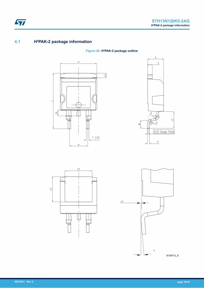
4.1 H²PAK-2 package information
Figure 20. H²PAK-2 package outline
8159712_8
STH13N120K5-2AGH²PAK-2 package information
DS12917 - Rev 3 page 10/16
Table 8. H²PAK-2 package mechanical data
Dim.mm
Min. Typ. Max.
A 4.30
-
4.70
A1 0.03 0.20
C 1.17 1.37
e 4.98 5.18
E 0.50 0.90
F 0.78 0.85
H 10.00 10.40
H1 7.40 7.80
L 15.30 15.80
L1 1.27 1.40
L2 4.93 5.23
L3 6.85 7.25
L4 1.5 1.7
M 2.6 2.9
R 0.20 0.60
V 0° 8°
Figure 21. H²PAK-2 recommended footprint
8159712_8
Note: Dimensions are in mm.
STH13N120K5-2AGH²PAK-2 package information
DS12917 - Rev 3 page 11/16
4.2 H²PAK-2 packing information
Figure 22. Tape outline
P1A0 D1
P0
FW
E
D
B0K0
T
User direction of feed
P2
10 pitches cumulativetolerance on tape +/- 0.2 mm
User direction of feed
R
Bending radius
Top covertape
AM08852v2
STH13N120K5-2AGPacking information
DS12917 - Rev 3 page 12/16
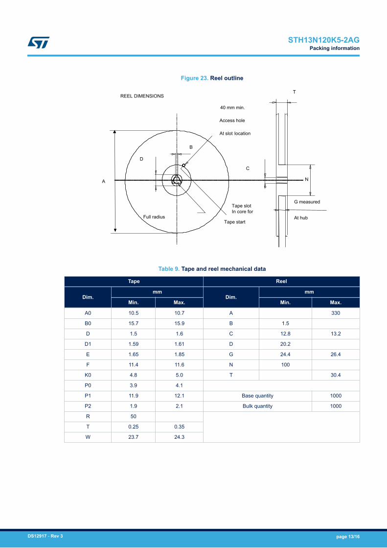
Figure 23. Reel outline
A
D
B
Full radius
Tape slotIn core for
Tape start
G measured
At hub
C
N
REEL DIMENSIONS
40 mm min.
Access hole
At slot location
T
Table 9. Tape and reel mechanical data
Tape Reel
Dim.mm
Dim.mm
Min. Max. Min. Max.
A0 10.5 10.7 A 330
B0 15.7 15.9 B 1.5
D 1.5 1.6 C 12.8 13.2
D1 1.59 1.61 D 20.2
E 1.65 1.85 G 24.4 26.4
F 11.4 11.6 N 100
K0 4.8 5.0 T 30.4
P0 3.9 4.1
P1 11.9 12.1 Base quantity 1000
P2 1.9 2.1 Bulk quantity 1000
R 50
T 0.25 0.35
W 23.7 24.3
STH13N120K5-2AGPacking information
DS12917 - Rev 3 page 13/16
Revision history
Table 10. Document revision history
Date Version Changes
14-Feb-2019 1 First release.
10-Sep-2019 2
Updated title and features in cover page.
Updated Section 1 Electrical ratings, Section 2 Electrical characteristics and
Section 2.1 Electrical characteristics (curves).
Minor text changes.
23-Oct-2019 3
Modified Table 1. Absolute maximum ratings, Table 2. Thermal data,Table 3. On/off states, Table 4. Dynamic, Table 5. Switching times andTable 6. Source-drain diode.
Modified Section 2.1 Electrical characteristics (curves).
STH13N120K5-2AG
DS12917 - Rev 3 page 14/16
Contents
1 Electrical ratings . . . . . . . . . . . . . . . . . . . . . . . . . . . . . . . . . . . . . . . . . . . . . . . . . . . . . . . . . . . . . . . . . .2
2 Electrical characteristics. . . . . . . . . . . . . . . . . . . . . . . . . . . . . . . . . . . . . . . . . . . . . . . . . . . . . . . . . . .3
2.1 Electrical characteristics (curves) . . . . . . . . . . . . . . . . . . . . . . . . . . . . . . . . . . . . . . . . . . . . . . . . . 5
3 Test circuits . . . . . . . . . . . . . . . . . . . . . . . . . . . . . . . . . . . . . . . . . . . . . . . . . . . . . . . . . . . . . . . . . . . . . . .8
4 Package information. . . . . . . . . . . . . . . . . . . . . . . . . . . . . . . . . . . . . . . . . . . . . . . . . . . . . . . . . . . . . . .9
4.1 H²PAK-2 package information . . . . . . . . . . . . . . . . . . . . . . . . . . . . . . . . . . . . . . . . . . . . . . . . . . . . 9
4.2 H²PAK-2 packing information. . . . . . . . . . . . . . . . . . . . . . . . . . . . . . . . . . . . . . . . . . . . . . . . . . . . 11
Revision history . . . . . . . . . . . . . . . . . . . . . . . . . . . . . . . . . . . . . . . . . . . . . . . . . . . . . . . . . . . . . . . . . . . . . . .14
STH13N120K5-2AGContents
DS12917 - Rev 3 page 15/16
IMPORTANT NOTICE – PLEASE READ CAREFULLY
STMicroelectronics NV and its subsidiaries (“ST”) reserve the right to make changes, corrections, enhancements, modifications, and improvements to STproducts and/or to this document at any time without notice. Purchasers should obtain the latest relevant information on ST products before placing orders. STproducts are sold pursuant to ST’s terms and conditions of sale in place at the time of order acknowledgement.
Purchasers are solely responsible for the choice, selection, and use of ST products and ST assumes no liability for application assistance or the design ofPurchasers’ products.
No license, express or implied, to any intellectual property right is granted by ST herein.
Resale of ST products with provisions different from the information set forth herein shall void any warranty granted by ST for such product.
ST and the ST logo are trademarks of ST. For additional information about ST trademarks, please refer to www.st.com/trademarks. All other product or servicenames are the property of their respective owners.
Information in this document supersedes and replaces information previously supplied in any prior versions of this document.
© 2019 STMicroelectronics – All rights reserved
STH13N120K5-2AG
DS12917 - Rev 3 page 16/16