DATA SHEET SE5516A: Dual-Band 802.11a/b/g/n/ac WLAN Front ...
17
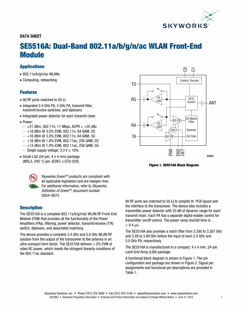
Skyworks Solutions, Inc. • Phone [781] 376-3000 • Fax [781] 376-3100 • [email protected] • www.skyworksinc.com 202396J • Skyworks Proprietary Information • Products and Product Information are Subject to Change Without Notice • June 27, 2019 1 DATA SHEET SE5516A: Dual-Band 802.11a/b/g/n/ac WLAN Front-End Module Applications 802.11a/b/g/n/ac WLANs Computing, networking Features All RF ports matched to 50 Ω Integrated 2.4 GHz PA, 5 GHz PA, transmit filter, transmit/receive switches, and diplexers Integrated power detector for each transmit chain Power: +21 dBm, 802.11b, 11 Mbps, ACPR = +35 dBc +18 dBm @ 3.0% EVM, 802.11n, 64 QAM, 2G +16 dBm @ 3.0% EVM, 802.11n, 64 QAM, 5G +16 dBm @ 1.8% EVM, 802.11ac, 256 QAM, 2G +13 dBm @ 1.8% EVM, 802.11ac, 256 QAM, 5G Single supply voltage: 3.3 V ± 10% Small LGA (24-pin, 4 x 4 mm) package (MSL3, 240 C per JEDEC J-STD-020) Skyworks Green TM products are compliant with all applicable legislation and are halogen-free. For additional information, refer to Skyworks Definition of Green TM , document number SQ04–0074. Description The SE5516A is a complete 802.11a/b/g/n/ac WLAN RF Front-End Module (FEM) that provides all the functionality of the Power Amplifiers (PAs), filtering, power detector, transmit/receive (T/R) switch, diplexers, and associated matching. The device provides a complete 2.4 GHz and 5.0 GHz WLAN RF solution from the output of the transceiver to the antenna in an ultra-compact form factor. The SE5516A delivers < 2% EVM at rated AC power, which meets the stringent linearity conditions of the 802.11ac standard. 5G LNA 5G PA 2G PA Control, Decode S2932 C0 C1 ANT RA RG TG TA ENA ENG DET 2G LNA SP3T Switch Det Diplexer 5G Filter 2G Match Filter Figure 1. SE5516A Block Diagram All RF ports are matched to 50 Ω to simplify th PCB layout and the interface to the transceiver. The device also includes a transmitter power detector with 20 dB of dynamic range for each transmit chain. Each PA has a separate digital enable control for transmitter on/off control. The power ramp rise/fall time is < 0.4 μs. The SE5516A also provides a notch filter from 3.260 to 3.267 GHz and 3.28 to 3.89 GHz before the input of each 2.4 GHz and 5.0 GHz PA, respectively. The SE5516A is manufactured in a compact, 4 x 4 mm, 24-pin Land Grid Array (LGA) package. A functional block diagram is shown in Figure 1. The pin configuration and package are shown in Figure 2. Signal pin assignments and functional pin descriptions are provided in Table 1.
Transcript of DATA SHEET SE5516A: Dual-Band 802.11a/b/g/n/ac WLAN Front ...
Skyworks Solutions, Inc. • Phone [781] 376-3000 • Fax [781] 376-3100 • [email protected] • www.skyworksinc.com 202396J • Skyworks Proprietary Information • Products and Product Information are Subject to Change Without Notice • June 27, 2019 1
DATA SHEET
SE5516A: Dual-Band 802.11a/b/g/n/ac WLAN Front-End Module Applications
802.11a/b/g/n/ac WLANs
Computing, networking
Features
All RF ports matched to 50 Ω
Integrated 2.4 GHz PA, 5 GHz PA, transmit filter, transmit/receive switches, and diplexers
Integrated power detector for each transmit chain
Power: +21 dBm, 802.11b, 11 Mbps, ACPR = +35 dBc +18 dBm @ 3.0% EVM, 802.11n, 64 QAM, 2G +16 dBm @ 3.0% EVM, 802.11n, 64 QAM, 5G +16 dBm @ 1.8% EVM, 802.11ac, 256 QAM, 2G +13 dBm @ 1.8% EVM, 802.11ac, 256 QAM, 5G Single supply voltage: 3.3 V ± 10%
Small LGA (24-pin, 4 x 4 mm) package (MSL3, 240 C per JEDEC J-STD-020)
Skyworks GreenTM products are compliant withall applicable legislation and are halogen-free.For additional information, refer to SkyworksDefinition of GreenTM, document number SQ04–0074.
Description The SE5516A is a complete 802.11a/b/g/n/ac WLAN RF Front-End Module (FEM) that provides all the functionality of the Power Amplifiers (PAs), filtering, power detector, transmit/receive (T/R) switch, diplexers, and associated matching.
The device provides a complete 2.4 GHz and 5.0 GHz WLAN RF solution from the output of the transceiver to the antenna in an ultra-compact form factor. The SE5516A delivers < 2% EVM at rated AC power, which meets the stringent linearity conditions of the 802.11ac standard.
5GLNA
5G PA
2G PA
Control, Decode
S2932
C0 C1
ANT
RA
RG
TG
TA
ENA
ENG
DET
2GLNA
SP3TSwitch
Det Diplexer
5G Filter
2G MatchFilter
Figure 1. SE5516A Block Diagram
All RF ports are matched to 50 Ω to simplify th PCB layout and the interface to the transceiver. The device also includes a transmitter power detector with 20 dB of dynamic range for each transmit chain. Each PA has a separate digital enable control for transmitter on/off control. The power ramp rise/fall time is < 0.4 μs.
The SE5516A also provides a notch filter from 3.260 to 3.267 GHz and 3.28 to 3.89 GHz before the input of each 2.4 GHz and 5.0 GHz PA, respectively.
The SE5516A is manufactured in a compact, 4 x 4 mm, 24-pin Land Grid Array (LGA) package.
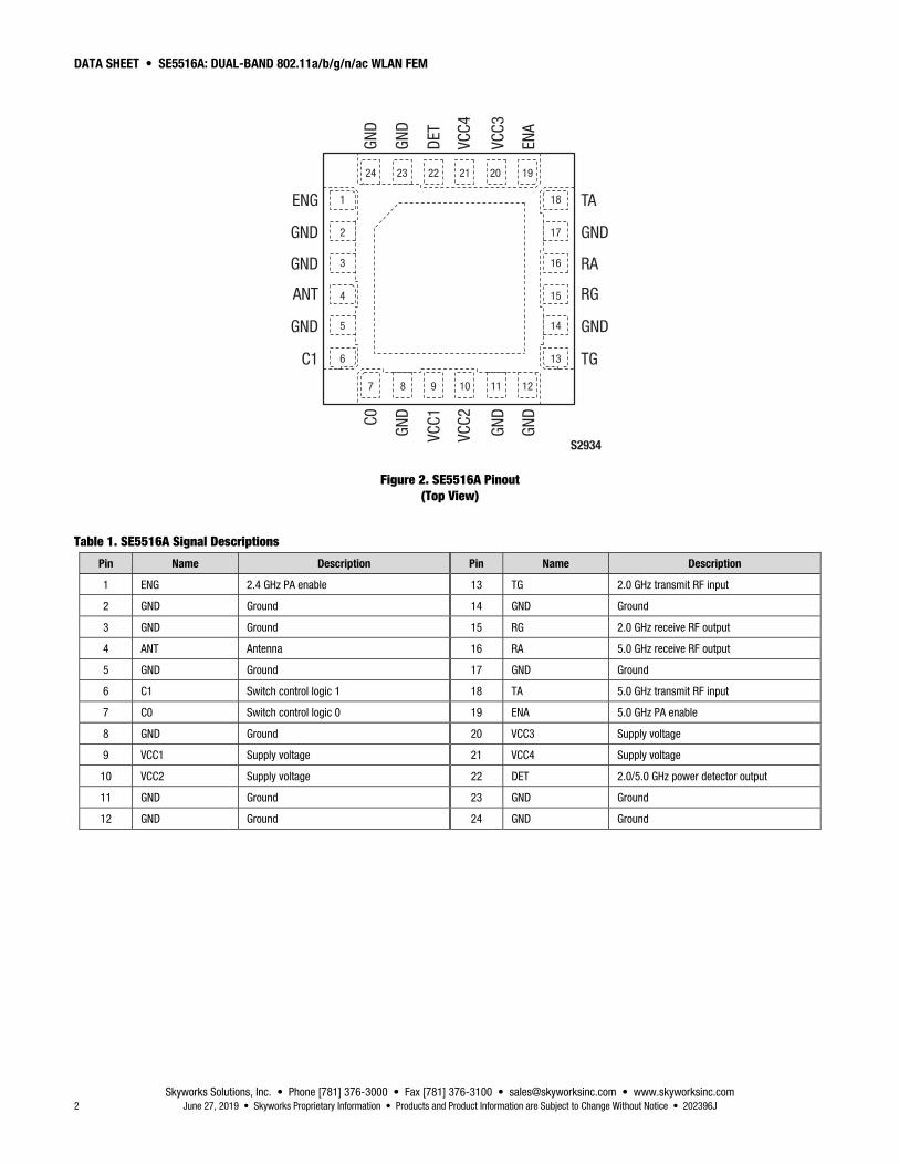
A functional block diagram is shown in Figure 1. The pin configuration and package are shown in Figure 2. Signal pin assignments and functional pin descriptions are provided in Table 1.
DATA SHEET • SE5516A: DUAL-BAND 802.11a/b/g/n/ac WLAN FEM
Skyworks Solutions, Inc. • Phone [781] 376-3000 • Fax [781] 376-3100 • [email protected] • www.skyworksinc.com 2 June 27, 2019 • Skyworks Proprietary Information • Products and Product Information are Subject to Change Without Notice • 202396J
S2934
1ENG
GND
GND
ANT
GND
C1C0
GND
VCC1
VCC2
GND
GND
GND
GND
DET
VCC4
VCC3
ENA
TA
GND
RA
RG
GND
TG
2
3
4
5
6
7 8 9 10 11 12
13
14
15
16
17
18
192021222324
Figure 2. SE5516A Pinout (Top View)
Table 1. SE5516A Signal Descriptions
Pin Name Description Pin Name Description
1 ENG 2.4 GHz PA enable 13 TG 2.0 GHz transmit RF input
2 GND Ground 14 GND Ground
3 GND Ground 15 RG 2.0 GHz receive RF output
4 ANT Antenna 16 RA 5.0 GHz receive RF output
5 GND Ground 17 GND Ground
6 C1 Switch control logic 1 18 TA 5.0 GHz transmit RF input
7 C0 Switch control logic 0 19 ENA 5.0 GHz PA enable
8 GND Ground 20 VCC3 Supply voltage
9 VCC1 Supply voltage 21 VCC4 Supply voltage
10 VCC2 Supply voltage 22 DET 2.0/5.0 GHz power detector output
11 GND Ground 23 GND Ground
12 GND Ground 24 GND Ground
DATA SHEET • SE5516A: DUAL-BAND 802.11a/b/g/n/ac WLAN FEM
Skyworks Solutions, Inc. • Phone [781] 376-3000 • Fax [781] 376-3100 • [email protected] • www.skyworksinc.com 202396H • Skyworks Proprietary Information • Products and Product Information are Subject to Change Without Notice • February 11, 2014 3
Electrical and Mechanical Specifications The absolute maximum ratings of the SE5516A are provided in Table 2. The recommended operating conditions are specified in Table 3.
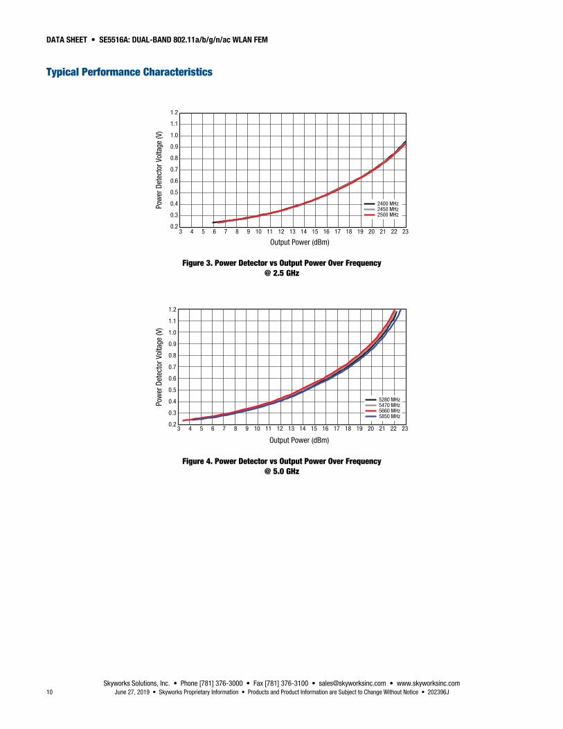
Electrical specifications are provided in Tables 4 through 12. Typical performance characteristics of the SE5516A are illustrated in Figures 3 and 4.
Table 2. SE5516A Absolute Maximum Ratings1
Parameter Symbol Minimum Maximum Units
Supply voltage VCC -0.3 +3.6 V
PA enable voltage (pins ENA and ENG) -0.3 +3.6 V
Maximum input power to TA and TG pins with ANT terminated in 6:1 load or better:
@ +25C @ -40C
PIN
+12 +5
dBm dBm
Operating temperature TA -40 +85 C
Storage temperature TSTG -40 +150 C
Switch logic control C0, C1 0 3.6 V
LNA power (receive mode) PRX -3 dBm
Electrostatic discharge:
ANT pin, Human Body Model (HBM), Class 1C All other pins, HBM, Class 1A
ESD
1000 250
V V
1 Exposure to maximum rating conditions for extended periods may reduce device reliability. There is no damage to device with only one parameter set at the limit and all other parameters set at or below their nominal value. Exceeding any of the limits listed here may result in permanent damage to the device.
ESD HANDLING: Although this device is designed to be as robust as possible, electrostatic discharge (ESD) can damage this device. This device must be protected at all times from ESD when handling or transporting. Static charges may easily produce potentials of several kilovolts on the human body or equipment, which can discharge without detection. Industry-standard ESD handling precautions should be used at all times.
Table 3. SE5516A Recommended Operating Conditions
Parameter Symbol Min Typ Max Units
Supply voltage VCC 3.0 3.3 3.6 V
Operating temperature TA -40 +25 +85 C
Junction temperature TJ +150 C
DATA SHEET • SE5516A: DUAL-BAND 802.11a/b/g/n/ac WLAN FEM
Skyworks Solutions, Inc. • Phone [781] 376-3000 • Fax [781] 376-3100 • [email protected] • www.skyworksinc.com 4 June 27, 2019 • Skyworks Proprietary Information • Products and Product Information are Subject to Change Without Notice • 202396J
Table 4. SE5516A Electrical Specifications: DC Characteristics1 (VCC = 3.3 V, TA = +25 C, All Unused Ports Terminated with 50 Ω, Unless Otherwise Noted)
Parameter Symbol Test Condition Min Typ Max Units
Total 802.11a transmit supply current
ICQ_A
ICC_A
No RF
POUT = +16 dBm, 54 Mbps, OFDM signal, 64 QAM
175
230
210
255
mA
mA
Total 802.11g transmit supply current
ICQ_G
ICC_G
No RF
POUT = +18 dBm, 54 Mbps, OFDM signal, 64 QAM
135
175
165
195
mA
mA
Total 802.11b transmit supply current ICC_B POUT = +21 dBm,
11 Mbps, CCK signal, BT = 0.45
200 220 mA
Total 802.11ac transmit supply current, 2G ICC_AC2G POUT = +16 dBm,
256 QAM, MCS9, 40 MHz 155 175 mA
Total 802.11ac transmit supply current, 5G ICC_AC5G POUT = +13 dBm,
256 QAM, MCS9, 80 MHz 190 215 mA
Total receive supply current, 2G ICC_RX2 ENG = ENA = 0 V, LNA on,
switch condition 1 12 mA
Total receive supply current, 5G ICC_RX5 ENG = ENA = 0 V, LNA on,
switch condition 4 12 mA
Total supply current ICC_OFF No RF, ENG = ENA = 0 V,
switch condition 3 or 6 50 μA
1 Performance is guaranteed only under the conditions listed in this table.
Table 5. SE5516A Electrical Specifications: Logic Characteristics1 (VCC = 3.3 V, TA = +25 C, All Unused Ports Terminated with 50 Ω, Unless Otherwise Noted)
Parameter Symbol Test Condition Min Typ Max Units
Logic high voltage for ENG and ENA (module on)
VENH 1.8 VCC V
Logic low voltage for ENG and ENA (module off)
VENL 0 0.5 V
Input current logic high voltage (ENG and ENA)
IENH 350 400 μA
Input current logic low voltage (ENG and ENA)
IENL 0.2 μA
1 Performance is guaranteed only under the conditions listed in this table.
DATA SHEET • SE5516A: DUAL-BAND 802.11a/b/g/n/ac WLAN FEM
Skyworks Solutions, Inc. • Phone [781] 376-3000 • Fax [781] 376-3100 • [email protected] • www.skyworksinc.com 202396J • Skyworks Proprietary Information • Products and Product Information are Subject to Change Without Notice • June 27, 2019 5
Table 6. SE5516A Electrical Specifications: Switch Characteristics1 (VCC = VEN = 3.3 V, TA = +25 C, All Unused Ports Terminated with 50 Ω, Unless Otherwise Noted)
Parameter Symbol Test Condition Min Typ Max Units
Control voltage (on state) VCTL_ON 3.0 3.6 V
Control voltage (off state) VCTL_OFF 0 0.2 V
Low loss switch control voltage SWON High state = VCTL_ON - VCTL_OFF
2.8 VCC V
High loss switch control voltage SWOFF Low state = VCTL_OFF - VCTL_OFF
0 0.3 V
Switch control bias current RF applied No RF
ICTL_ON C0 and C1 pins driven high
100 30
μA μA
Control input capacitance CCTL 100 pF 1 Performance is guaranteed only under the conditions listed in this table.
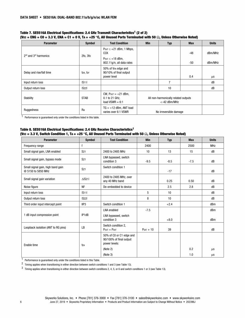
Table 7. SE5516A Electrical Specifications: 2.4 GHz Transmit Characteristics1 (1 of 2) (VCC = ENG = C0 = 3.3 V, ENA = C1 = 0 V, TA = +25 C, All Unused Ports Terminated with 50 Ω, Unless Otherwise Noted)
Parameter Symbol Test Condition Min Typ Max Units
Frequency range f 2400 2500 MHz
Output power, 802.11g POUT_802.11G
54 Mbps OFDM signal, 64 QAM, DEVM = 3%, input signal EVM < 1%, 802.11g mask compliant +18 dBm
Output power, 802.11n POUT_802.11N
OFDM signal, MCS7, HT40, DEVM = 3%, 802.11n mask compliant, ±11 MHz offset, RBW = 100 kHz, VBW = 30 kHz
DEVM = 2.5%
+18
+17
dBm
dBm
Output power, 802.11ac POUT_802.11AC
40 MHz, 256 QAM, MCS9, DEVM = 1.8%, 802.11ac mask compliant
DEVM = 1.4%
+16
+15
dBm
dBm
Output power, 802.11b POUT_802.11B
11 Mbps CCK signal, BT = 0.45, ACPR (±11 MHz offset) < -35, ACPR (±22 MHz offset) < -56 +21 dBm
1 dB compression point P1dB +24.0 +24.5 dBm
Small signal gain |S21| 25 31 dB
Small signal gain variation over any 40 MHz channel
Δ|S21| Switch state 2 0.5 1.0 dB
Small signal gain variation over band Δ|S21| 1 2 dB
Small signal gain @ ½ VCO frequency |S21|_1.6 1608 to 1656 MHz 12 20 dB
Small signal gain @ VCO frequency |S21|_3.2 3216 to 3312 MHz 1206 to 1242 MHz 3618 to 3726 MHz
0 +12 -10
dB dB dB
DATA SHEET • SE5516A: DUAL-BAND 802.11a/b/g/n/ac WLAN FEM
Skyworks Solutions, Inc. • Phone [781] 376-3000 • Fax [781] 376-3100 • [email protected] • www.skyworksinc.com 6 June 27, 2019 • Skyworks Proprietary Information • Products and Product Information are Subject to Change Without Notice • 202396J
Table 7. SE5516A Electrical Specifications: 2.4 GHz Transmit Characteristics1 (2 of 2) (VCC = ENG = C0 = 3.3 V, ENA = C1 = 0 V, TA = +25 C, All Unused Ports Terminated with 50 Ω, Unless Otherwise Noted)
Parameter Symbol Test Condition Min Typ Max Units
2nd and 3rd harmonics 2fo, 3fo
POUT ≤ +21 dBm, 1 Mbps, CCK
POUT ≤ +18 dBm, 802.11g/n, all data rates
-48
-50
dBm/MHz
dBm/MHz
Delay and rise/fall time tDR, tDF 50% of VEN edge and 90/10% of final output power level 0.4 μs
Input return loss |S11| 7 dB
Output return loss |S22| 10 dB
Stability STAB CW, POUT = +21 dBm, 0.1 to 21 GHz, load VSWR = 6:1
All non-harmonically related outputs <-42 dBm/MHz
Ruggedness Ru TG = +12 dBm, ANT load varies over 6:1 VSWR No irreversible damage
1 Performance is guaranteed only under the conditions listed in this table.
Table 8. SE5516A Electrical Specifications: 2.4 GHz Receive Characteristics1 (VCC = 3.3 V, Switch Condition 1, TA = +25 C, All Unused Ports Terminated with 50 Ω, Unless Otherwise Noted)
Parameter Symbol Test Condition Min Typ Max Units
Frequency range f 2400 2500 MHz
Small signal gain, LNA enabled S21 2400 to 2485 MHz 10 13 15 dB
Small signal gain, bypass mode S21 LNA bypassed, switch condition 3 -9.5 -8.5 -7.5 dB
Small signal gain, high band gain @ 5150 to 5850 MHz
S21 Switch condition 1
-17 dB
Small signal gain variation Δ|S21| 2400 to 2485 MHz, over any 40 MHz band 0.25 0.50 dB
Noise figure NF De-embedded to device 2.5 2.8 dB
Input return loss |S11| 5 10 dB
Output return loss |S22| 8 10 dB
Third order input intercept point IIP3 Switch condition 1 +2.4 dBm
1 dB input compression point IP1dB
LNA enabled
LNA bypassed, switch condition 3
-7.5
+8.0
dBm
dBm
Loopback isolation (ANT to RG pins) LB Switch condition 2, POUT = PSAT PSAT + 10 39 dB
Enable time tEN
50% of C0 or C1 edge and 90/100% of final output power levels:
(Note 2)
(Note 3)
0.2
1.0
μs
μs 1 Performance is guaranteed only under the conditions listed in this Table. 2 Timing applies when transitioning in either direction between switch conditions 1 and 3 (see Table 13). 3 Timing applies when transitioning in either direction between switch conditions 2, 4, 5, or 6 and switch conditions 1 or 3 (see Table 13).
DATA SHEET • SE5516A: DUAL-BAND 802.11a/b/g/n/ac WLAN FEM
Skyworks Solutions, Inc. • Phone [781] 376-3000 • Fax [781] 376-3100 • [email protected] • www.skyworksinc.com 202396J • Skyworks Proprietary Information • Products and Product Information are Subject to Change Without Notice • June 27, 2019 7
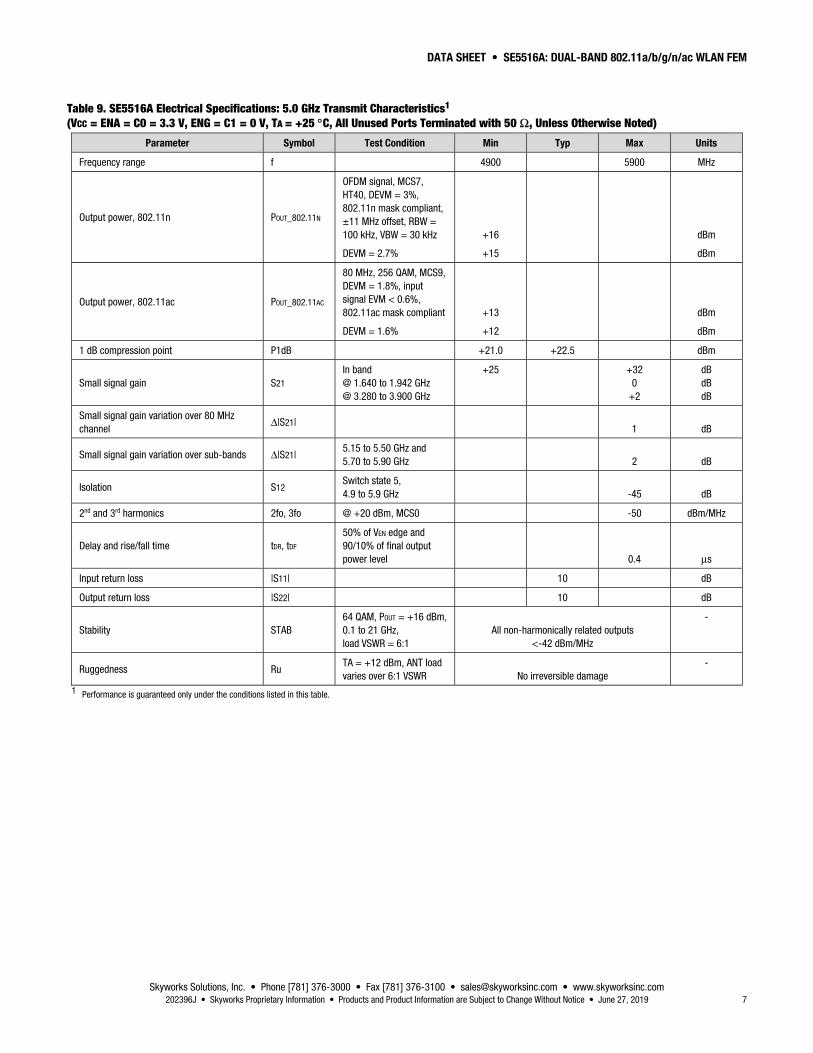
Table 9. SE5516A Electrical Specifications: 5.0 GHz Transmit Characteristics1 (VCC = ENA = C0 = 3.3 V, ENG = C1 = 0 V, TA = +25 C, All Unused Ports Terminated with 50 Ω, Unless Otherwise Noted)
Parameter Symbol Test Condition Min Typ Max Units
Frequency range f 4900 5900 MHz
Output power, 802.11n POUT_802.11N
OFDM signal, MCS7, HT40, DEVM = 3%, 802.11n mask compliant, ±11 MHz offset, RBW = 100 kHz, VBW = 30 kHz
DEVM = 2.7%
+16
+15
dBm
dBm
Output power, 802.11ac POUT_802.11AC
80 MHz, 256 QAM, MCS9, DEVM = 1.8%, input signal EVM < 0.6%, 802.11ac mask compliant
DEVM = 1.6%
+13
+12
dBm
dBm
1 dB compression point P1dB +21.0 +22.5 dBm
Small signal gain S21 In band @ 1.640 to 1.942 GHz @ 3.280 to 3.900 GHz
+25 +32 0
+2
dB dB dB
Small signal gain variation over 80 MHz channel
Δ|S21|
1 dB
Small signal gain variation over sub-bands Δ|S21| 5.15 to 5.50 GHz and 5.70 to 5.90 GHz 2 dB
Isolation S12 Switch state 5, 4.9 to 5.9 GHz -45 dB
2nd and 3rd harmonics 2fo, 3fo @ +20 dBm, MCS0 -50 dBm/MHz
Delay and rise/fall time tDR, tDF 50% of VEN edge and 90/10% of final output power level 0.4 μs
Input return loss |S11| 10 dB
Output return loss |S22| 10 dB
Stability STAB 64 QAM, POUT = +16 dBm, 0.1 to 21 GHz, load VSWR = 6:1
All non-harmonically related outputs <-42 dBm/MHz
-
Ruggedness Ru TA = +12 dBm, ANT load varies over 6:1 VSWR No irreversible damage
-
1 Performance is guaranteed only under the conditions listed in this table.
DATA SHEET • SE5516A: DUAL-BAND 802.11a/b/g/n/ac WLAN FEM
Skyworks Solutions, Inc. • Phone [781] 376-3000 • Fax [781] 376-3100 • [email protected] • www.skyworksinc.com 8 June 27, 2019 • Skyworks Proprietary Information • Products and Product Information are Subject to Change Without Notice • 202396J
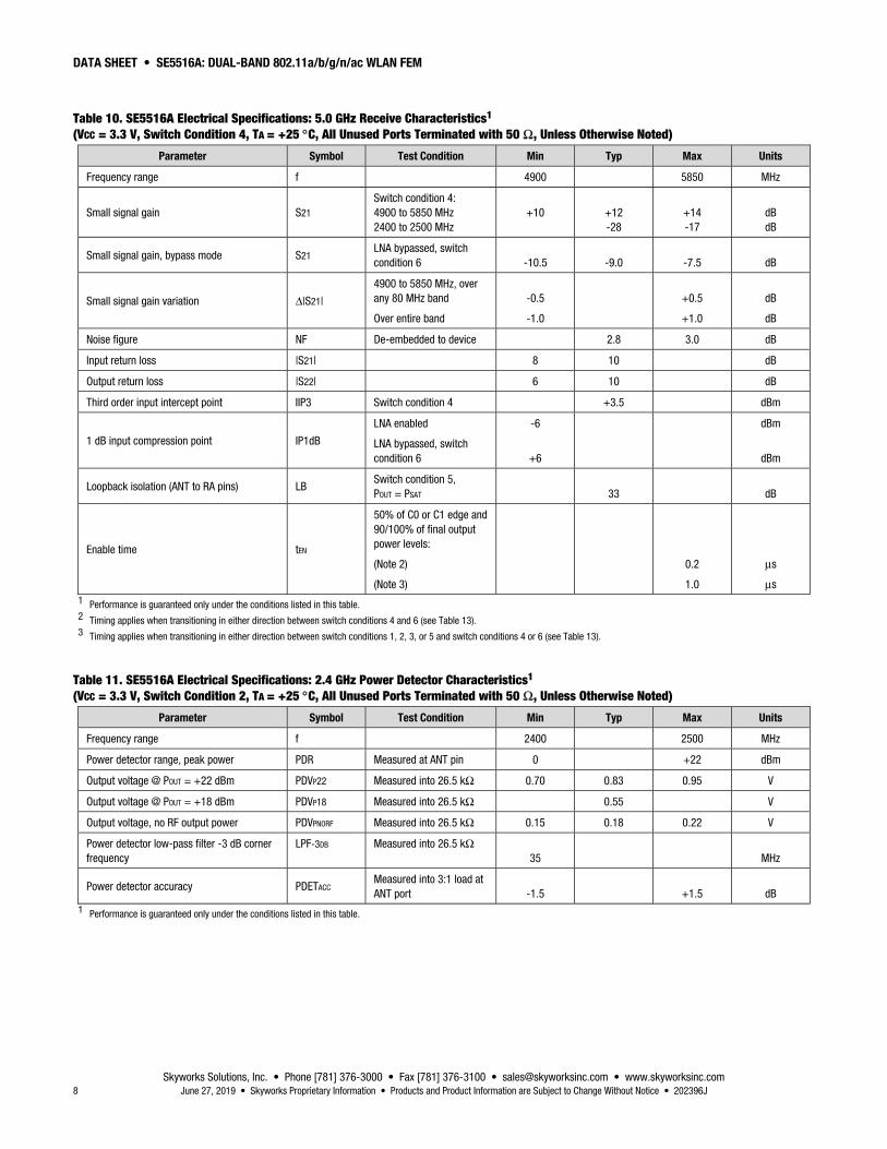
Table 10. SE5516A Electrical Specifications: 5.0 GHz Receive Characteristics1 (VCC = 3.3 V, Switch Condition 4, TA = +25 C, All Unused Ports Terminated with 50 Ω, Unless Otherwise Noted)
Parameter Symbol Test Condition Min Typ Max Units
Frequency range f 4900 5850 MHz
Small signal gain S21 Switch condition 4: 4900 to 5850 MHz 2400 to 2500 MHz
+10
+12 -28
+14 -17
dB dB
Small signal gain, bypass mode S21 LNA bypassed, switch condition 6 -10.5 -9.0 -7.5 dB
Small signal gain variation Δ|S21|
4900 to 5850 MHz, over any 80 MHz band
Over entire band
-0.5
-1.0
+0.5
+1.0
dB
dB
Noise figure NF De-embedded to device 2.8 3.0 dB
Input return loss |S21| 8 10 dB
Output return loss |S22| 6 10 dB
Third order input intercept point IIP3 Switch condition 4 +3.5 dBm
1 dB input compression point IP1dB
LNA enabled
LNA bypassed, switch condition 6
-6
+6
dBm
dBm
Loopback isolation (ANT to RA pins) LB Switch condition 5, POUT = PSAT 33 dB
Enable time tEN
50% of C0 or C1 edge and 90/100% of final output power levels:
(Note 2)
(Note 3)
0.2
1.0
μs
μs 1 Performance is guaranteed only under the conditions listed in this table. 2 Timing applies when transitioning in either direction between switch conditions 4 and 6 (see Table 13). 3 Timing applies when transitioning in either direction between switch conditions 1, 2, 3, or 5 and switch conditions 4 or 6 (see Table 13).
Table 11. SE5516A Electrical Specifications: 2.4 GHz Power Detector Characteristics1 (VCC = 3.3 V, Switch Condition 2, TA = +25 C, All Unused Ports Terminated with 50 Ω, Unless Otherwise Noted)
Parameter Symbol Test Condition Min Typ Max Units
Frequency range f 2400 2500 MHz
Power detector range, peak power PDR Measured at ANT pin 0 +22 dBm
Output voltage @ POUT = +22 dBm PDVP22 Measured into 26.5 kΩ 0.70 0.83 0.95 V
Output voltage @ POUT = +18 dBm PDVP18 Measured into 26.5 kΩ 0.55 V
Output voltage, no RF output power PDVPNORF Measured into 26.5 kΩ 0.15 0.18 0.22 V
Power detector low-pass filter -3 dB corner frequency
LPF-3DB Measured into 26.5 kΩ 35 MHz
Power detector accuracy PDETACC Measured into 3:1 load at ANT port -1.5 +1.5 dB
1 Performance is guaranteed only under the conditions listed in this table.
DATA SHEET • SE5516A: DUAL-BAND 802.11a/b/g/n/ac WLAN FEM
Skyworks Solutions, Inc. • Phone [781] 376-3000 • Fax [781] 376-3100 • [email protected] • www.skyworksinc.com 202396J • Skyworks Proprietary Information • Products and Product Information are Subject to Change Without Notice • June 27, 2019 9
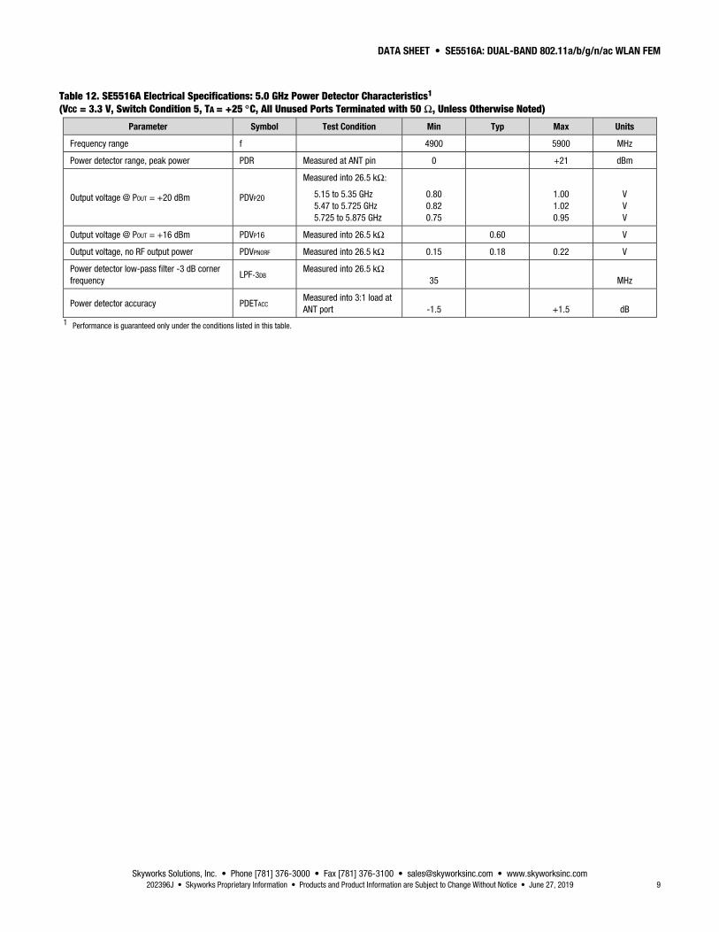
Table 12. SE5516A Electrical Specifications: 5.0 GHz Power Detector Characteristics1 (VCC = 3.3 V, Switch Condition 5, TA = +25 C, All Unused Ports Terminated with 50 Ω, Unless Otherwise Noted)
Parameter Symbol Test Condition Min Typ Max Units
Frequency range f 4900 5900 MHz
Power detector range, peak power PDR Measured at ANT pin 0 +21 dBm
Output voltage @ POUT = +20 dBm PDVP20
Measured into 26.5 kΩ:
5.15 to 5.35 GHz 5.47 to 5.725 GHz 5.725 to 5.875 GHz
0.80 0.82 0.75
1.00 1.02 0.95
V V V
Output voltage @ POUT = +16 dBm PDVP16 Measured into 26.5 kΩ 0.60 V
Output voltage, no RF output power PDVPNORF Measured into 26.5 kΩ 0.15 0.18 0.22 V
Power detector low-pass filter -3 dB corner frequency
LPF-3DB Measured into 26.5 kΩ
35 MHz
Power detector accuracy PDETACC Measured into 3:1 load at ANT port -1.5 +1.5 dB
1 Performance is guaranteed only under the conditions listed in this table.
DATA SHEET • SE5516A: DUAL-BAND 802.11a/b/g/n/ac WLAN FEM
Skyworks Solutions, Inc. • Phone [781] 376-3000 • Fax [781] 376-3100 • [email protected] • www.skyworksinc.com 10 June 27, 2019 • Skyworks Proprietary Information • Products and Product Information are Subject to Change Without Notice • 202396J
Typical Performance Characteristics
0.2
0.3
0.4
0.5
0.6
0.7
0.8
0.9
1.0
1.1
1.2
3 4 5 6 7 8 9 10 11 12 13 14 15 16 17 18 19 20 21 22 23
Output Power (dBm)
Pow
er D
etec
tor V
olta
ge (V
)
2400 MHz2450 MHz2500 MHz
Figure 3. Power Detector vs Output Power Over Frequency @ 2.5 GHz
0.2
0.3
0.4
0.5
0.6
0.7
0.8
0.9
1.0
1.1
1.2
3 4 5 6 7 8 9 10 11 12 13 14 15 16 17 18 19 20 21 22 23
Output Power (dBm)
Pow
er D
etec
tor V
olta
ge (V
)
5280 MHz5470 MHz5660 MHz5850 MHz
Figure 4. Power Detector vs Output Power Over Frequency @ 5.0 GHz
DATA SHEET • SE5516A: DUAL-BAND 802.11a/b/g/n/ac WLAN FEM
Skyworks Solutions, Inc. • Phone [781] 376-3000 • Fax [781] 376-3100 • [email protected] • www.skyworksinc.com 202396J • Skyworks Proprietary Information • Products and Product Information are Subject to Change Without Notice • June 27, 2019 11
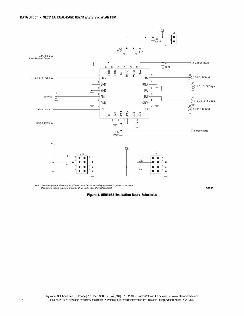
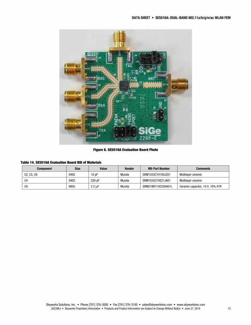
Evaluation Board Description The SE5516A Evaluation Board is used to test the performance of the SE5516A WLAN FEM. An Evaluation Board schematic diagram is provided in Figure 5. A photograph of the Evaluation Board is shown in Figure 6. Component values for the SE5516A Evaluation Board are listed in Table 14.
Evaluation Board Setup Procedure
Step 1: Connect system ground to pin 2 of connector J6.
Step 2: Apply 3.3 V to pin 1 of connector J6.
Step 3: Select a path according to the logic shown in Table 13.
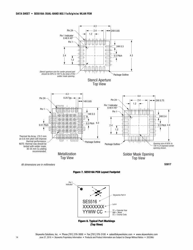
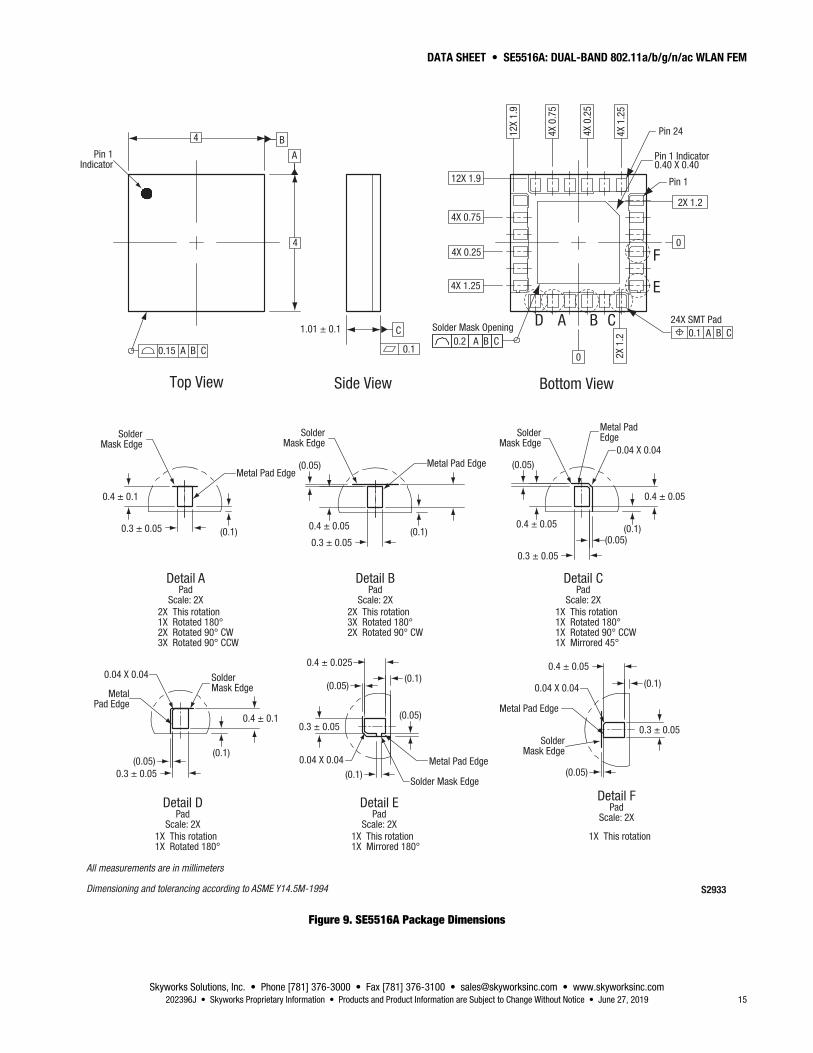
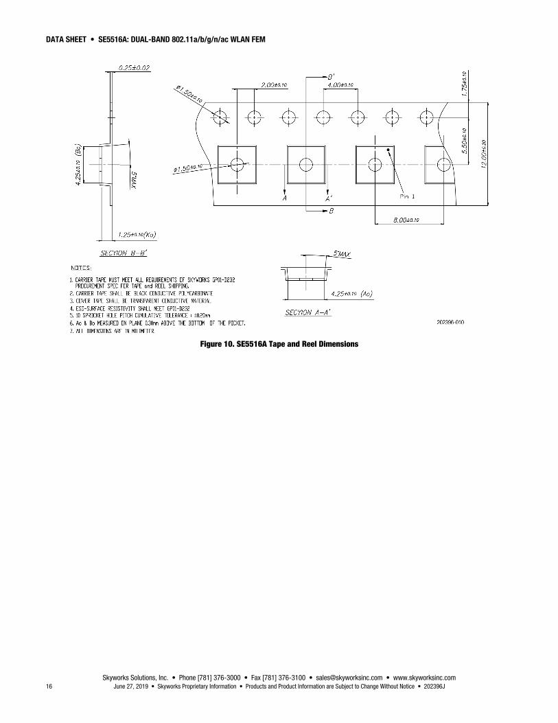
Package Dimensions The PCB layout footprint for the SE5516A is provided in Figure 7. Typical part markings are shown in Figure 8. Package dimensions are shown in Figure 9, and tape and reel dimensions are provided in Figure 10.
Package and Handling Information Since the device package is sensitive to moisture absorption, it is baked and vacuum packed before shipping. Instructions on the shipping container label regarding exposure to moisture after the container seal is broken must be followed. Otherwise, problems related to moisture absorption may occur when the part is subjected to high temperature during solder assembly.
The SE5516A is rated to Moisture Sensitivity Level 3 (MSL3) at 240 C. It can be used for lead or lead-free soldering. For additional information, refer to the Skyworks Application Note, Solder Reflow Information, document number 200164.
Care must be taken when attaching this product, whether it is done manually or in a production solder reflow environment. Production quantities of this product are shipped in a standard tape and reel format.
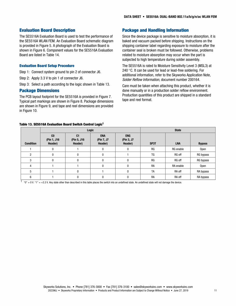
Table 13. SE5516A Evaluation Board Switch Control Logic1
Condition
Logic State
C0 (Pin 1, J16
Header)
C1 (Pin 5, J16
Header)
ENA (Pin 7, J7 Header)
ENG (Pin 3, J7 Header) SP3T LNA Bypass
1 0 1 0 0 RG RG enable Open
2 0 0 0 1 TG RG off RG bypass
3 0 0 0 0 RG RG off RG bypass
4 1 1 0 0 RA RA enable Open
5 1 0 1 0 TA RA off RA bypass
6 1 0 0 0 RA RA off RA bypass 1 “0” = 0 V. “1” = +3.3 V. Any state other than described in this table places the switch into an undefined state. An undefined state will not damage the device.
DATA SHEET • SE5516A: DUAL-BAND 802.11a/b/g/n/ac WLAN FEM
Skyworks Solutions, Inc. • Phone [781] 376-3000 • Fax [781] 376-3100 • [email protected] • www.skyworksinc.com 12 June 27, 2019 • Skyworks Proprietary Information • Products and Product Information are Subject to Change Without Notice • 202396J
2.4 GHz PA Enable
Antenna
2 GHz Tx RF Input
5 GHz Tx RF Input
5 GHz PA Enable
5 GHz Rx RF Output
2 GHz Rx RF Output
S2935
J5
J4
J3
J2
J1
J16
3
1C0
C1 5
7
4
2
6
8
2.4/5.0 GHzPower Detector Output
Switch Control
Supply Voltage
J6
2
1
C82.2 μF
C4220 pF
C610 pF
VCC
1ENG
GND
GND
ANT
GND
C1C0 GN
D
VCC1
VCC2
GND
GND
GND
GND
DET
VCC4
VCC3 EN
A
TA
GND
RA
RG
GND
TG
2
3
4
5
6
7 8 9 10 11 12
13
14
15
16
17
18
192021222324C210 pF
C510 pF
Switch Control
Note: Some component labels may be different than the corresponding component symbol shown here. Component values, however, are accurate as of the date of this Data Sheet.
VCC
J7
3
1DET
ENA
5
ENG
7
4
2
6
8
VCC
Figure 5. SE5516A Evaluation Board Schematic
DATA SHEET • SE5516A: DUAL-BAND 802.11a/b/g/n/ac WLAN FEM
Skyworks Solutions, Inc. • Phone [781] 376-3000 • Fax [781] 376-3100 • [email protected] • www.skyworksinc.com 202396J • Skyworks Proprietary Information • Products and Product Information are Subject to Change Without Notice • June 27, 2019 13
Figure 6. SE5516A Evaluation Board Photo
Table 14. SE5516A Evaluation Board Bill of Materials
Component Size Value Vendor Mfr Part Number Comments
C2, C5, C6 0402 10 pF Murata GRM1555C1H100JZ01 Multilayer ceramic
C4 0402 220 pF Murata GRM1555C1H221JA01 Multilayer ceramic
C8 0805 2.2 μF Murata GRM21BR71A225KA01L Ceramic capacitor, 10 V, 10% X7R
DATA SHEET • SE5516A: DUAL-BAND 802.11a/b/g/n/ac WLAN FEM
Skyworks Solutions, Inc. • Phone [781] 376-3000 • Fax [781] 376-3100 • [email protected] • www.skyworksinc.com 14 June 27, 2019 • Skyworks Proprietary Information • Products and Product Information are Subject to Change Without Notice • 202396J
4.3
4.3
S3017
Pin 24
Pin 1
Pin 1 Indicator0.40 X 45°
Pin 24
Pin 1
Pin 1 Indicator0.40 X 45°
Pin 24
Pin 1
24X 0.65
24X 0.3
0.5 Pitch
4.4
24X 0.4
0.5 Pitch0.51 Pitch
2.4
1.2
2.4
1.2
4.3
14X 0.3
0.5 Pitch
Package Outline
Package OutlinePackage Outline
2.41.2
4.4
24X 0.752.41.2
4.3
0.25 Typ.14X 0.65
Stencil aperture size for center ground padshould be 80% to 100 % (by area) of the
solder mask opening.
Opening size of 60% to100 % of exposed centeropening shown.
Stencil ApertureTop View
MetallizationTop View
Solder Mask OpeningTop View
Thermal Via Array, ∅0.3 mmon 0.6 mm pitch will improve
thermal performance.NOTE: thermal vias should be
tented with solder mask,30-35 mm Cu plating
recommended.
All dimensions are in millimeters
Figure 7. SE5516A PCB Layout Footprint
Pin 1Indicator
Skyworks Part #
Lot #
YY = Calendar YearWW = WeekCC = County Code
Figure 8. Typical Part Markings (Top View)
DATA SHEET • SE5516A: DUAL-BAND 802.11a/b/g/n/ac WLAN FEM
Skyworks Solutions, Inc. • Phone [781] 376-3000 • Fax [781] 376-3100 • [email protected] • www.skyworksinc.com 202396J • Skyworks Proprietary Information • Products and Product Information are Subject to Change Without Notice • June 27, 2019 15
All measurements are in millimeters
Dimensioning and tolerancing according to ASME Y14.5M-1994
4
4
Pin 1Indicator
Metal Pad Edge
SolderMask Edge
1.01 ± 0.1
(0.1)
Side View
B
Bottom ViewTop View
Pin 24
F
E
CBAD
Pin 1
Pin 1 Indicator0.40 X 0.40
0.4 ± 0.1
0.4 ± 0.1
0.3 ± 0.050.3 ± 0.05
0.3 ± 0.05
0.3 ± 0.05
0.3 ± 0.05
0.3 ± 0.05
0.4 ± 0.05
0.4 ± 0.025
0.4 ± 0.05
0.4 ± 0.05
0.4 ± 0.05
(0.1)
(0.1)
(0.1) (0.1)
(0.05)(0.1)
(0.1)
(0.05)
(0.05)
(0.05)
(0.05)
(0.05)
(0.05)
Solder Mask Opening24X SMT Pad
Metal Pad Edge
SolderMask Edge
MetalPad Edge
Metal Pad Edge
0.15 A B C0.2 A B C
0.1 A B C
A
C
0.1
SolderMask Edge
SolderMask Edge
Metal Pad Edge
Solder Mask Edge
Metal PadEdge
0.04 X 0.04
SolderMask Edge
0.04 X 0.040.04 X 0.04
0.04 X 0.04
4X 0.75
4X 0.25
4X 1.25
12X 1.9
2X 1.2
0
0
4X 0
.75
4X 0
.25
4X 1
.25
12X
1.9
2X 1
.2
Detail APad
Scale: 2X2X This rotation1X Rotated 180°2X Rotated 90° CW3X Rotated 90° CCW
Detail BPad
Scale: 2X2X This rotation3X Rotated 180°2X Rotated 90° CW
Detail DPad
Scale: 2X1X This rotation1X Rotated 180°
Detail CPad
Scale: 2X1X This rotation1X Rotated 180°1X Rotated 90° CCW1X Mirrored 45°
Detail EPad
Scale: 2X1X This rotation1X Mirrored 180°
Detail FPad
Scale: 2X
1X This rotation
S2933
Figure 9. SE5516A Package Dimensions
DATA SHEET • SE5516A: DUAL-BAND 802.11a/b/g/n/ac WLAN FEM
Skyworks Solutions, Inc. • Phone [781] 376-3000 • Fax [781] 376-3100 • [email protected] • www.skyworksinc.com 16 June 27, 2019 • Skyworks Proprietary Information • Products and Product Information are Subject to Change Without Notice • 202396J
Figure 10. SE5516A Tape and Reel Dimensions
DATA SHEET • SE5516A: DUAL-BAND 802.11a/b/g/n/ac WLAN FEM
Skyworks Solutions, Inc. • Phone [781] 376-3000 • Fax [781] 376-3100 • [email protected] • www.skyworksinc.com 202396J • Skyworks Proprietary Information • Products and Product Information are Subject to Change Without Notice • June 27, 2019 17
Ordering Information Part Number Product Description Evaluation Board Part Number
SE5516A Dual-Band 802.11a/b/g/n/ac WLAN FEM SE5516A-EK1
Copyright © 2012-2014, 2017, 2019 Skyworks Solutions, Inc. All Rights Reserved.
Information in this document is provided in connection with Skyworks Solutions, Inc. (“Skyworks”) products or services. These materials, including the information contained herein, are provided by Skyworks as a service to its customers and may be used for informational purposes only by the customer. Skyworks assumes no responsibility for errors or omissions in these materials or the information contained herein. Skyworks may change its documentation, products, services, specifications or product descriptions at any time, without notice. Skyworks makes no commitment to update the materials or information and shall have no responsibility whatsoever for conflicts, incompatibilities, or other difficulties arising from any future changes.
No license, whether express, implied, by estoppel or otherwise, is granted to any intellectual property rights by this document. Skyworks assumes no liability for any materials, products or information provided hereunder, including the sale, distribution, reproduction or use of Skyworks products, information or materials, except as may be provided in Skyworks Terms and Conditions of Sale.
THE MATERIALS, PRODUCTS AND INFORMATION ARE PROVIDED “AS IS” WITHOUT WARRANTY OF ANY KIND, WHETHER EXPRESS, IMPLIED, STATUTORY, OR OTHERWISE, INCLUDING FITNESS FOR A PARTICULAR PURPOSE OR USE, MERCHANTABILITY, PERFORMANCE, QUALITY OR NON-INFRINGEMENT OF ANY INTELLECTUAL PROPERTY RIGHT; ALL SUCH WARRANTIES ARE HEREBY EXPRESSLY DISCLAIMED. SKYWORKS DOES NOT WARRANT THE ACCURACY OR COMPLETENESS OF THE INFORMATION, TEXT, GRAPHICS OR OTHER ITEMS CONTAINED WITHIN THESE MATERIALS. SKYWORKS SHALL NOT BE LIABLE FOR ANY DAMAGES, INCLUDING BUT NOT LIMITED TO ANY SPECIAL, INDIRECT, INCIDENTAL, STATUTORY, OR CONSEQUENTIAL DAMAGES, INCLUDING WITHOUT LIMITATION, LOST REVENUES OR LOST PROFITS THAT MAY RESULT FROM THE USE OF THE MATERIALS OR INFORMATION, WHETHER OR NOT THE RECIPIENT OF MATERIALS HAS BEEN ADVISED OF THE POSSIBILITY OF SUCH DAMAGE.
Skyworks products are not intended for use in medical, lifesaving or life-sustaining applications, or other equipment in which the failure of the Skyworks products could lead to personal injury, death, physical or environmental damage. Skyworks customers using or selling Skyworks products for use in such applications do so at their own risk and agree to fully indemnify Skyworks for any damages resulting from such improper use or sale.
Customers are responsible for their products and applications using Skyworks products, which may deviate from published specifications as a result of design defects, errors, or operation of products outside of published parameters or design specifications. Customers should include design and operating safeguards to minimize these and other risks. Skyworks assumes no liability for applications assistance, customer product design, or damage to any equipment resulting from the use of Skyworks products outside of stated published specifications or parameters.
Skyworks and the Skyworks symbol are trademarks or registered trademarks of Skyworks Solutions, Inc. or its subsidiaries in the United States and other countries. Third-party brands and names are for identification purposes only, and are the property of their respective owners. Additional information, including relevant terms and conditions, posted at www.skyworksinc.com, are incorporated by reference.