COMPONENTS - docs-apac.rs-online.com · 3 03/01/2014 ICPL0630, ICPL0631 ISOCOM COMPONENTS DC93175...
13
1 03/01/2014 ICPL0630, ICPL0631 ISOCOM COMPONENTS DC93175 DESCRIPTION The ICPL0630 and ICPL0631 dual channel devices each consists of an infrared emitting diode optically coupled to a high speed photo detector transistor. These devices belong to Isocom Compact Range of optocouplers. FEATURES • High speed 10Mbit/s • Half Pitch 1.27mm • 10kV/μs min. Common Mode Transient Immunity • (ICPL0631) • High AC Isolation Voltage 3750V RMS • Guaranteed Performance from -40°C to 85°C • Wide Operating Temperature Range • -40°C to 100°C • Pb Free and RoHS Compliant • Halogen Free • Safety Approvals Pending APPLICATIONS • Line Receivers, Data Communication • LSTTL to TTL, LSTTL or 5V CMOS • Data Multiplexing • Pulse Transformer Replacement • Switch Mode Power Supplies • Ground Loop Elimination • Computer Peripheral Interface ORDER INFORMATION • Available in Tape and Reel with 2000pcs per reel. ISOCOM COMPONENTS 2004 LTD Unit 25B, Park View Road West, Park View Industrial Estate Hartlepool, Cleveland, TS25 1UD, United Kingdom Tel: +44 (0)1429 863 609 Fax : +44 (0)1429 863 581 e-mail: [email protected] http://www.isocom.com ISOCOM COMPONENTS ASIA LTD Hong Kong Office, Block A, 8/F, Wah Hing Industrial mansion, 36 Tai Yau Street, San Po Kong, Kowloon, Hong Kong. Tel: +852 2995 9217 Fax : +852 8161 6292 e-mail [email protected] ABSOLUTE MAXIMUM RATINGS (T A = 25°C) Input Diode Forward Current 20mA Reverse Voltage 5V Power dissipation 45mW Output Output Current 50mA Output Voltage 7V Supply Voltage (max 1 min) 7V Power Dissipation 60mW Total Package Isolation Voltage 3750V RMS Total Power Dissipation 80mW Operating Temperature -40 to 100 °C Storage Temperature -55 to 125 °C Lead Soldering Temperature (10s) 260°C 1. Anode (Channel1) 2. Cathode (Channel 1) 3. Cathode (Channel 2) 4. Anode (Channel 2) 5. GND 6. Vout 2 7. Vout 1 8. Vcc A 0.1μF bypass capacitor must be connected between Vcc (pins 8) and GND (pin 5).
Transcript of COMPONENTS - docs-apac.rs-online.com · 3 03/01/2014 ICPL0630, ICPL0631 ISOCOM COMPONENTS DC93175...

1 03/01/2014
ICPL0630, ICPL0631
ISOCOM COMPONENTS
DC93175
DESCRIPTION
The ICPL0630 and ICPL0631 dual channel devices each consists of an infrared emitting diode optically coupled to a high speed photo detector transistor. These devices belong to Isocom Compact Range of optocouplers.
FEATURES • High speed 10Mbit/s • Half Pitch 1.27mm • 10kV/μs min. Common Mode Transient Immunity • (ICPL0631) • High AC Isolation Voltage 3750VRMS • Guaranteed Performance from -40°C to 85°C • Wide Operating Temperature Range • -40°C to 100°C • Pb Free and RoHS Compliant • Halogen Free • Safety Approvals Pending APPLICATIONS • Line Receivers, Data Communication • LSTTL to TTL, LSTTL or 5V CMOS • Data Multiplexing • Pulse Transformer Replacement • Switch Mode Power Supplies • Ground Loop Elimination • Computer Peripheral Interface ORDER INFORMATION • Available in Tape and Reel with 2000pcs
per reel.
ISOCOM COMPONENTS 2004 LTD Unit 25B, Park View Road West, Park View Industrial Estate
Hartlepool, Cleveland, TS25 1UD, United Kingdom Tel: +44 (0)1429 863 609 Fax : +44 (0)1429 863 581
e-mail: [email protected] http://www.isocom.com
ISOCOM COMPONENTS ASIA LTD Hong Kong Office,
Block A, 8/F, Wah Hing Industrial mansion, 36 Tai Yau Street, San Po Kong, Kowloon, Hong Kong.
Tel: +852 2995 9217 Fax : +852 8161 6292 e-mail [email protected]
ABSOLUTE MAXIMUM RATINGS (TA = 25°C) Input Diode Forward Current 20mA Reverse Voltage 5V Power dissipation 45mW Output Output Current 50mA Output Voltage 7V Supply Voltage (max 1 min) 7V Power Dissipation 60mW Total Package Isolation Voltage 3750VRMS Total Power Dissipation 80mW Operating Temperature -40 to 100 °C Storage Temperature -55 to 125 °C Lead Soldering Temperature (10s) 260°C
1. Anode (Channel1) 2. Cathode (Channel 1) 3. Cathode (Channel 2) 4. Anode (Channel 2) 5. GND 6. Vout 2 7. Vout 1 8. Vcc
A 0.1μF bypass capacitor must be connected between Vcc (pins 8) and GND (pin 5).
2 03/01/2014
ICPL0630, ICPL0631
ISOCOM COMPONENTS
DC93175
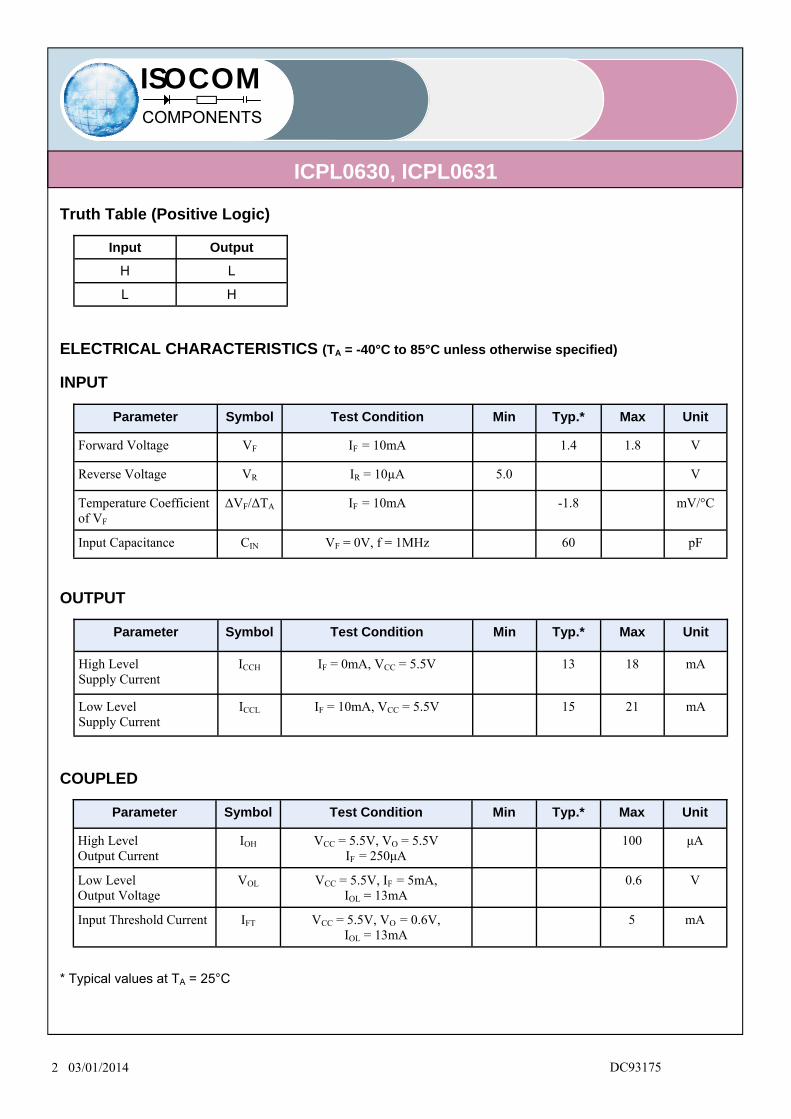
Truth Table (Positive Logic)
ELECTRICAL CHARACTERISTICS (TA = -40°C to 85°C unless otherwise specified) INPUT OUTPUT COUPLED * Typical values at TA = 25°C
Parameter Symbol Test Condition Min Typ.* Max Unit
Forward Voltage VF IF = 10mA 1.4 1.8 V
Reverse Voltage VR IR = 10µA 5.0 V
Temperature Coefficient of VF
ΔVF/ΔTA IF = 10mA -1.8 mV/°C
Input Capacitance CIN VF = 0V, f = 1MHz 60 pF
Parameter Symbol Test Condition Min Typ.* Max Unit
High Level Supply Current
ICCH IF = 0mA, VCC = 5.5V 13 18 mA
Low Level Supply Current
ICCL IF = 10mA, VCC = 5.5V 15 21 mA
Input Output
H L
L H
Parameter Symbol Test Condition Min Typ.* Max Unit
High Level Output Current
IOH VCC = 5.5V, VO = 5.5V IF = 250μA
100 μA
Low Level Output Voltage
VOL VCC = 5.5V, IF = 5mA, IOL = 13mA
0.6 V
Input Threshold Current IFT VCC = 5.5V, VO = 0.6V, IOL = 13mA
5 mA

3 03/01/2014
ICPL0630, ICPL0631
ISOCOM COMPONENTS
DC93175
ELECTRICAL CHARACTERISTICS (TA = -40°C to 85°C unless otherwise specified) Switching Characteristics (TA = -40°C to 85°C, IF = 7.5mA, VCC = 5V unless otherwise specified) * Typical values at TA = 25°C
Parameter Symbol Test Condition Min Typ.* Max Unit
Propagation Delay Time to Logic Low
TPHL RL = 350Ω, CL = 15pF, TA = 25°C
100 ns
Propagation Delay Time to Logic High
TPLH RL = 350Ω, CL = 15pF, TA = 25°C
100
ns
Pulse Width Distortion |tPHL-tPLH| RL = 350Ω, CL = 15pF 35 ns
Output Rise Time tr RL = 350Ω, CL = 15pF 40 ns
Output Fall Time tf RL = 350Ω, CL = 15pF 10 ns
Common Mode Transient Immunity at Logic High
CMH ICPL0630
IF = 0mA, VOH = 2.0V, VCM = 1kVp-p,
RL = 350Ω, TA = 25°C
5000
V/μs
ICPL0631
IF = 0mA, VOH = 2.0V, VCM = 1kVp-p,
RL = 350Ω, TA = 25°C
10000
Common Mode Transient Immunity at Logic Low
CML V/μs ICPL0630
IF = 7.5mA, VOL = 0.8V, VCM = 1kVp-p,
RL = 350Ω, TA = 25°C
5000
ICPL0631
IF = 7.5mA, VOL = 0.8V, VCM = 1kVp-p,
RL = 350Ω, TA = 25°C
10000

4 03/01/2014
ICPL0630, ICPL0631
ISOCOM COMPONENTS
DC93175
ELECTRICAL CHARACTERISTICS Notes : 1. The VCC supply must be bypassed by a 0.1μF capacitor or larger with good high frequency characteristic and
should be connected as close as possible to the package VCC and GND pins. 2. tPLH – Propagation delay is measured from the 3.75mA level on the HIGH to LOW transition of the input current
pulse to the 1.5 V level on the LOW to HIGH transition of the output voltage pulse. 3. tPHL – Propagation delay is measured from the 3.75mA level on the LOW to HIGH transition of the input current
pulse to the 1.5 V level on the HIGH to LOW transition of the output voltage pulse. 4 tr – Rise time is measured from the 10% to the 90% levels on the LOW to HIGH transition of the output pulse. 5. tf – Fall time is measured from the 90% to the 10% levels on the HIGH to LOW transition of the output pulse. 6. CMH – The maximum tolerable rate of rise of the common mode voltage to ensure the output will remain in the
HIGH state (i.e., VOUT > 2.0V). 7. CML – The maximum tolerable rate of rise of the common mode voltage to ensure the output will remain in the
LOW output state (i.e., VOUT < 0.8V).

5 03/01/2014
ICPL0630, ICPL0631
ISOCOM COMPONENTS
DC93175
Fig 1 Forward Current vs Forward Voltage Fig 2 Output Voltage vs Forward Current
Fig 3 Input Threshold Current vs TA Fig 4 Low Level Output Voltage vs TA
Fig 5 Low Level Output Current vs TA Fig 6 High Level Output Current vs TA

6 03/01/2014
ICPL0630, ICPL0631
ISOCOM COMPONENTS
DC93175
Fig 7 Propagation Delay vs Forward Current Fig 8 Propagation Delay vs TA
Fig 9 Pulse Width Distortion vs TA Fig 10 Rise and Fall Time vs TA

7 03/01/2014
ICPL0630, ICPL0631
ISOCOM COMPONENTS
DC93175
Common mode transient immunity in logic high level is the maximum tolerable (positive) dVCM/dt on the leading edge of
the common mode pulse signal VCM, to assure that the output will remain in a logic high state (i.e., VO > 2.0V). Common mode transient immunity in logic low level is the maximum tolerable (negative) dVCM/dt on the trailing edge of
the common mode pulse signal, VCM, to assure that the output will remain in a logic low state (i.e., VO < 0.8V).
Fig 11 Switching Time Test Circuit
Fig 12 Common Mode Transient Immunity Test Circuit
10%
90%
Output (VO)
Output (VO)
Input (IF)
IF=7.5mA
IF=3.75mA
1.5V
tr tf
tPLH
tPHL
IF=7.5mA
IF=0mA
CML
CMH
VO(Min)
VO(Max)
Peak
VCM 0V
5V VO
VO
0.5V

8 03/01/2014
ICPL0630, ICPL0631
ISOCOM COMPONENTS
DC93175
ORDER INFORMATION
DEVICE MARKING ICPL0630 denotes Device Part Number (ICPL0630 is used as example) Y denotes 1 digit Year code WW denotes 2 digit Week code I denotes Isocom
ICPL0630, ICPL0631
After PN PN Description Packing quantity
None ICPL0630, ICPL0631 Surface Mount Tape & Reel 2000 pcs per reel
ICPL0630
IYWW
9 03/01/2014
ICPL0630, ICPL0631
ISOCOM COMPONENTS
DC93175
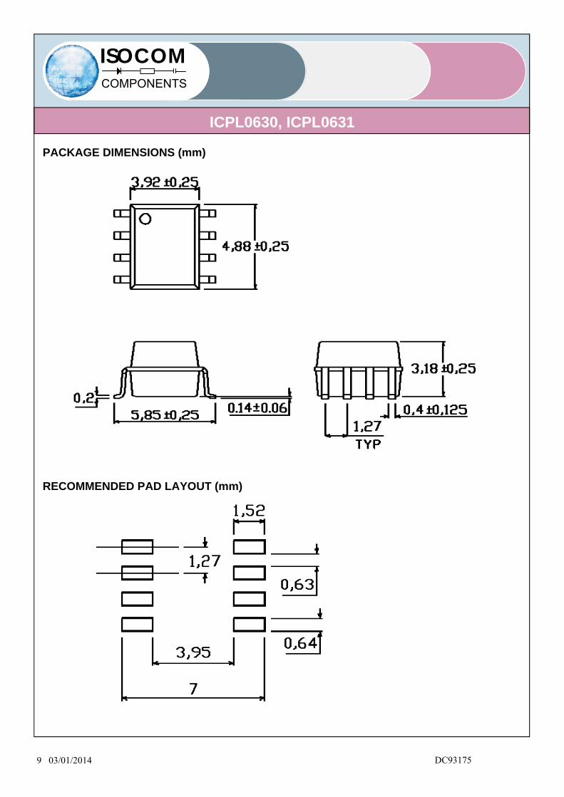
PACKAGE DIMENSIONS (mm)
RECOMMENDED PAD LAYOUT (mm)

10 03/01/2014
ICPL0630, ICPL0631
ISOCOM COMPONENTS
DC93175
IR REFLOW SOLDERING TEMPERATURE PROFILE (One Time Reflow Soldering is Recommended)
TIME (s)
TEM
P (°
C)
25°C
ts Preheat 60s – 120s
Tsmin
Tsmax
260°C
TL 217°C
Time 25°C to Peak Temperature
tP
TP - 5°C TP
Max Ramp Up Rate 3°C/s
Max Ramp Down Rate 6°C/s
TL 200°C
150°C
Profile Details Conditions
Preheat - Min Temperature (TSMIN) - Max Temperature (TSMAX) - Time TSMIN to TSMAX (ts)
150°C 200°C 60s - 120s
Soldering Zone - Peak Temperature (TP) - Liquidous Temperature (TL) - Time within 5°C of Actual Peak Temperature (TP 5°C) - Time maintained above TL (tL) - Ramp Up Rate (TL to TP) - Ramp Down Rate (TP to TL)
260°C 217°C 30s 60s - 100s 3°C/s max 6°C/s max
Average Ramp Up Rate (Tsmax to TP) 3°C/s max
Time 25°C to Peak Temperature 8 minutes max

11 03/01/2014
ICPL0630, ICPL0631
ISOCOM COMPONENTS
DC93175
TAPE AND REEL PACKAGING
Direction of feed from reel
Dimension No. A0 A1 B0 D0 D1 E F
Dimension (mm) 6.2±0.1 4.1±0.1 5.28±0.1 1.5±0.1 1.5±0.3 1.75±0.1 5.5±0.1
Dimension No. Po P1 P2 t W K0 K1
Dimension (mm) 4.0±0.1 8.0±0.1 2.0±0.1 0.4±0.1 12.0
+0.3/-0.1
3.7±0.1 0.3±0.1

12 03/01/2014
ICPL0630, ICPL0631
ISOCOM COMPONENTS
DC93175
NOTES : - Isocom is continually improving the quality, reliability, function or design and Isocom reserves the right to make
changes without further notices. - The products shown in this publication are designed for the general use in electronic applications such as
office automation equipment, communications devices, audio/visual equipment, electrical application and instrumentation.
- For equipment/application where high reliability or safety is required, such as space applications, nuclear power
control equipment, medical equipment, etc., please contact our sales representatives. - When requiring a device for any ”specific” application, please contact our sales for advice. - The contents described herein are subject to change without prior notice. - Do not immerse device body in solder paste.

13 05/12/2013
DISCLAIMER
ISOCOM COMPONENTS
Dxxxxxx
ISOCOM is continually working to improve the quality and reliability of its products. Nevertheless, semiconductor devices in general can malfunction or fail due to their inherent electrical sensitivity and vulnerability to physical stress. It is the responsibility of the buyer, when utilizing ISOCOM products, to comply with the standards of safety in making a safe design for the entire system, and to avoid situations in which a malfunction or failure of such ISOCOM products could cause loss of human life, bodily injury or damage to property. In developing your designs, please ensure that ISOCOM products are used within specified operating ranges as set forth in the most recent ISOCOM products specifications. __ The ISOCOM products listed in this document are intended for usage in general electronics applications (computer, personal equipment, office equipment, measuring equipment, industrial robotics, domestic appliances, etc.). These ISOCOM products are neither intended nor warranted for usage in equipment that requires extraordinarily high quality and/or reliability or a malfunction or failure of which may cause loss of human life or bodily injury (“Unintended Usage”). Unintended Usage include atomic energy control instruments, airplane or spaceship instruments, transportation Instruments, traffic signal instruments, combustion control instruments, medical Instruments, all types of safety devices, etc.. Unintended Usage of ISOCOM products listed in this document shall be made at the customer’s own risk. __ Gallium arsenide (GaAs) is a substance used in the products described in this document. GaAs dust and fumes are toxic. Do not break, cut or pulverize the product, or use chemicals to dissolve them. When disposing of the products, follow the appropriate regulations. Do not dispose of the products with other industrial waste or with domestic garbage. __ The products described in this document are subject to the foreign exchange and foreign trade laws. __ The information contained herein is presented only as a guide for the applications of our products. No responsibility is assumed by ISOCOM Components for any infringements of intellectual property or other rights of the third parties which may result from its use. No license is granted by implication or otherwise under any intellectual property or other rights of ISOCOM Components or others. __ The information contained herein is subject to change without notice