![RAIZ UNITÁRIA E COINTEGRAÇÃO: TR S APLICA*V *V ES · PDF filetransitório e passam a apresentar um caráter permanente [(Pereira, 1988) e (Gujarati, 2000)]. "A presença de uma](https://static.fdocument.org/doc/165x107/5a8a78e47f8b9adb648c00c5/raiz-unitria-e-cointegrao-tr-s-aplicav-v-es-e-passam-a-apresentar-um-carter-permanente.jpg)
50-MHz Low-Distortion High-CMRR Rail-to-Rail I/O, Single · PDF fileR 2 2k ! SD1 BAT17 C 1...
32
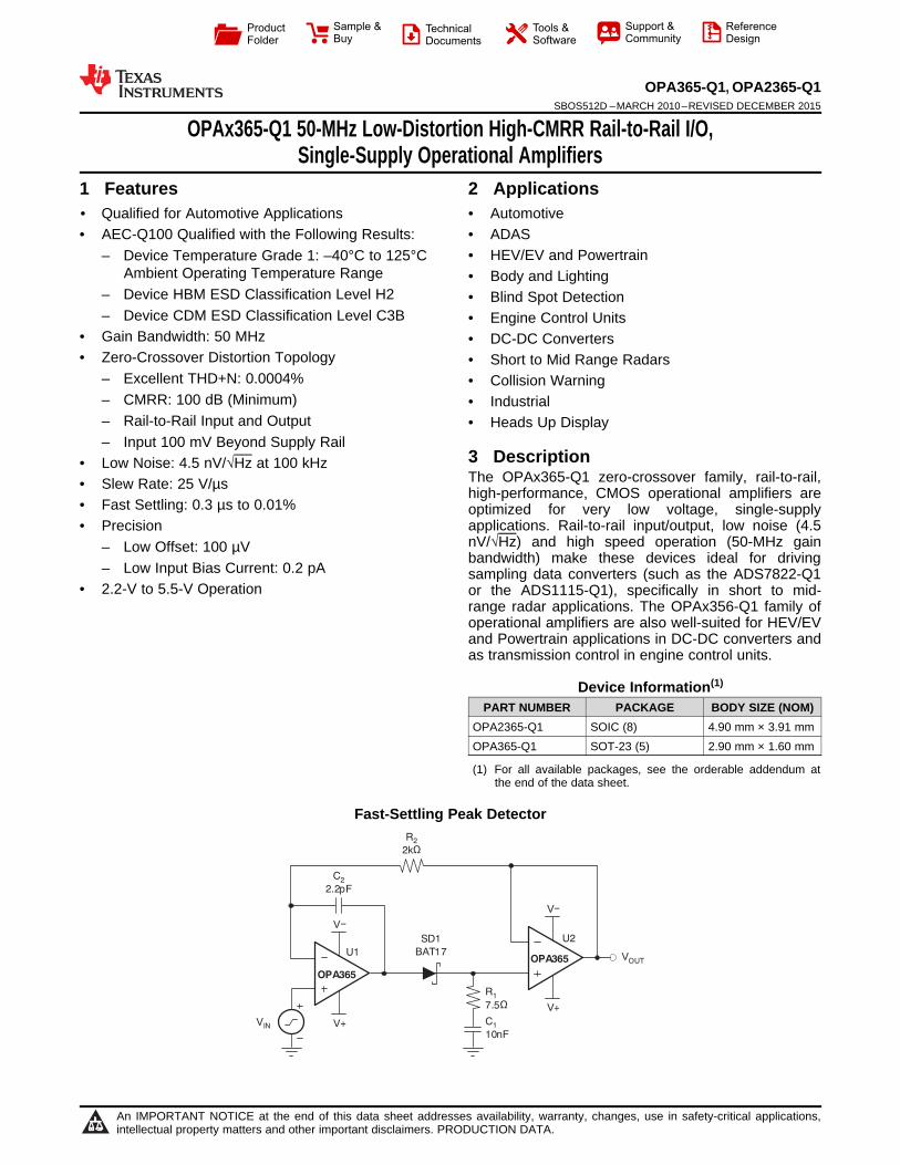
V IN V OUT C 2 2.2pF R 2 2kΩ SD1 BAT17 C 1 10nF R 1 7.5Ω V- V+ U1 U2 V- V+ OPA365 OPA365 Product Folder Sample & Buy Technical Documents Tools & Software Support & Community Reference Design OPA365-Q1, OPA2365-Q1 SBOS512D – MARCH 2010 – REVISED DECEMBER 2015 OPAx365-Q1 50-MHz Low-Distortion High-CMRR Rail-to-Rail I/O, Single-Supply Operational Amplifiers 1 Features 2 Applications 1• Qualified for Automotive Applications • Automotive • AEC-Q100 Qualified with the Following Results: • ADAS • HEV/EV and Powertrain – Device Temperature Grade 1: –40°C to 125°C Ambient Operating Temperature Range • Body and Lighting – Device HBM ESD Classification Level H2 • Blind Spot Detection – Device CDM ESD Classification Level C3B • Engine Control Units • Gain Bandwidth: 50 MHz • DC-DC Converters • Zero-Crossover Distortion Topology • Short to Mid Range Radars – Excellent THD+N: 0.0004% • Collision Warning – CMRR: 100 dB (Minimum) • Industrial – Rail-to-Rail Input and Output • Heads Up Display – Input 100 mV Beyond Supply Rail 3 Description • Low Noise: 4.5 nV/√Hz at 100 kHz The OPAx365-Q1 zero-crossover family, rail-to-rail, • Slew Rate: 25 V/μs high-performance, CMOS operational amplifiers are • Fast Settling: 0.3 μs to 0.01% optimized for very low voltage, single-supply applications. Rail-to-rail input/output, low noise (4.5 • Precision nV/√Hz) and high speed operation (50-MHz gain – Low Offset: 100 μV bandwidth) make these devices ideal for driving – Low Input Bias Current: 0.2 pA sampling data converters (such as the ADS7822-Q1 • 2.2-V to 5.5-V Operation or the ADS1115-Q1), specifically in short to mid- range radar applications. The OPAx356-Q1 family of operational amplifiers are also well-suited for HEV/EV and Powertrain applications in DC-DC converters and as transmission control in engine control units. Device Information (1) PART NUMBER PACKAGE BODY SIZE (NOM) OPA2365-Q1 SOIC (8) 4.90 mm × 3.91 mm OPA365-Q1 SOT-23 (5) 2.90 mm × 1.60 mm (1) For all available packages, see the orderable addendum at the end of the data sheet. Fast-Settling Peak Detector 1 An IMPORTANT NOTICE at the end of this data sheet addresses availability, warranty, changes, use in safety-critical applications, intellectual property matters and other important disclaimers. PRODUCTION DATA.
Transcript of 50-MHz Low-Distortion High-CMRR Rail-to-Rail I/O, Single · PDF fileR 2 2k ! SD1 BAT17 C 1...
VIN
VOUT
C2
2.2pF
R2
2kΩ
SD1
BAT17
C1
10nF
R1
7.5Ω
V−
V+
U1
U2
V−
V+
OPA365
OPA365
Product
Folder
Sample &Buy
Technical
Documents
Tools &
Software
Support &Community
ReferenceDesign
OPA365-Q1, OPA2365-Q1SBOS512D –MARCH 2010–REVISED DECEMBER 2015
OPAx365-Q1 50-MHz Low-Distortion High-CMRR Rail-to-Rail I/O,Single-Supply Operational Amplifiers
1 Features 2 Applications1• Qualified for Automotive Applications • Automotive• AEC-Q100 Qualified with the Following Results: • ADAS
• HEV/EV and Powertrain– Device Temperature Grade 1: –40°C to 125°CAmbient Operating Temperature Range • Body and Lighting
– Device HBM ESD Classification Level H2 • Blind Spot Detection– Device CDM ESD Classification Level C3B • Engine Control Units
• Gain Bandwidth: 50 MHz • DC-DC Converters• Zero-Crossover Distortion Topology • Short to Mid Range Radars
– Excellent THD+N: 0.0004% • Collision Warning– CMRR: 100 dB (Minimum) • Industrial– Rail-to-Rail Input and Output • Heads Up Display– Input 100 mV Beyond Supply Rail
3 Description• Low Noise: 4.5 nV/√Hz at 100 kHzThe OPAx365-Q1 zero-crossover family, rail-to-rail,• Slew Rate: 25 V/µs high-performance, CMOS operational amplifiers are
• Fast Settling: 0.3 µs to 0.01% optimized for very low voltage, single-supplyapplications. Rail-to-rail input/output, low noise (4.5• PrecisionnV/√Hz) and high speed operation (50-MHz gain– Low Offset: 100 µVbandwidth) make these devices ideal for driving
– Low Input Bias Current: 0.2 pA sampling data converters (such as the ADS7822-Q1• 2.2-V to 5.5-V Operation or the ADS1115-Q1), specifically in short to mid-
range radar applications. The OPAx356-Q1 family ofoperational amplifiers are also well-suited for HEV/EVand Powertrain applications in DC-DC converters andas transmission control in engine control units.
Device Information(1)
PART NUMBER PACKAGE BODY SIZE (NOM)OPA2365-Q1 SOIC (8) 4.90 mm × 3.91 mmOPA365-Q1 SOT-23 (5) 2.90 mm × 1.60 mm
(1) For all available packages, see the orderable addendum atthe end of the data sheet.
Fast-Settling Peak Detector
1
An IMPORTANT NOTICE at the end of this data sheet addresses availability, warranty, changes, use in safety-critical applications,intellectual property matters and other important disclaimers. PRODUCTION DATA.
OPA365-Q1, OPA2365-Q1SBOS512D –MARCH 2010–REVISED DECEMBER 2015 www.ti.com
Table of Contents8.4 Device Functional Modes........................................ 131 Features .................................................................. 1
9 Application and Implementation ........................ 142 Applications ........................................................... 19.1 Application Information............................................ 143 Description ............................................................. 19.2 Typical Application ................................................. 174 Revision History..................................................... 2
10 Power Supply Recommendations ..................... 205 Description (Continued) ........................................ 311 Layout................................................................... 206 Pin Configuration and Functions ......................... 3
11.1 Layout Guidelines ................................................. 207 Specifications......................................................... 411.2 Layout Example .................................................... 207.1 Absolute Maximum Ratings ...................................... 4
12 Device and Documentation Support ................. 217.2 ESD Ratings.............................................................. 412.1 Documentation Support ........................................ 217.3 Recommended Operating Conditions....................... 412.2 Related Links ........................................................ 217.4 Thermal Information .................................................. 412.3 Community Resources.......................................... 217.5 Electrical Characteristics........................................... 512.4 Trademarks ........................................................... 217.6 Typical Characteristics .............................................. 712.5 Electrostatic Discharge Caution............................ 218 Detailed Description ............................................ 1112.6 Glossary ................................................................ 218.1 Overview ................................................................. 11
13 Mechanical, Packaging, and Orderable8.2 Functional Block Diagram ....................................... 11Information ........................................................... 218.3 Feature Description................................................. 12
4 Revision HistoryNOTE: Page numbers for previous revisions may differ from page numbers in the current version.
Changes from Revision C (April 2012) to Revision D Page
• Added ESD Ratings table, Feature Description section, Device Functional Modes, Application and Implementationsection, Power Supply Recommendations section, Layout section, Device and Documentation Support section, andMechanical, Packaging, and Orderable Information section ................................................................................................. 1
Changes from Revision B (January 2012) to Revision C Page
• Added another row with VOS for OPA2365-Q1 only ............................................................................................................... 5• Changed IQ upper limit to 5.3 from 5.5 ................................................................................................................................... 6
2 Submit Documentation Feedback Copyright © 2010–2015, Texas Instruments Incorporated
Product Folder Links: OPA365-Q1 OPA2365-Q1
1
2
3
4 5
6
7
8
+IN B
−IN B
V BOUT
V+
V−
+IN A
−IN A
V AOUT1
2
3
5
4
V+
–IN+IN
V–
VOUT
OPA365-Q1, OPA2365-Q1www.ti.com SBOS512D –MARCH 2010–REVISED DECEMBER 2015
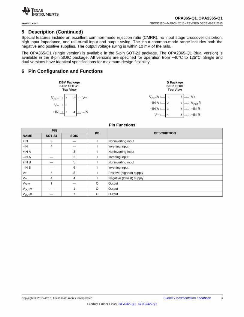
5 Description (Continued)Special features include an excellent common-mode rejection ratio (CMRR), no input stage crossover distortion,high input impedance, and rail-to-rail input and output swing. The input common-mode range includes both thenegative and positive supplies. The output voltage swing is within 10 mV of the rails.
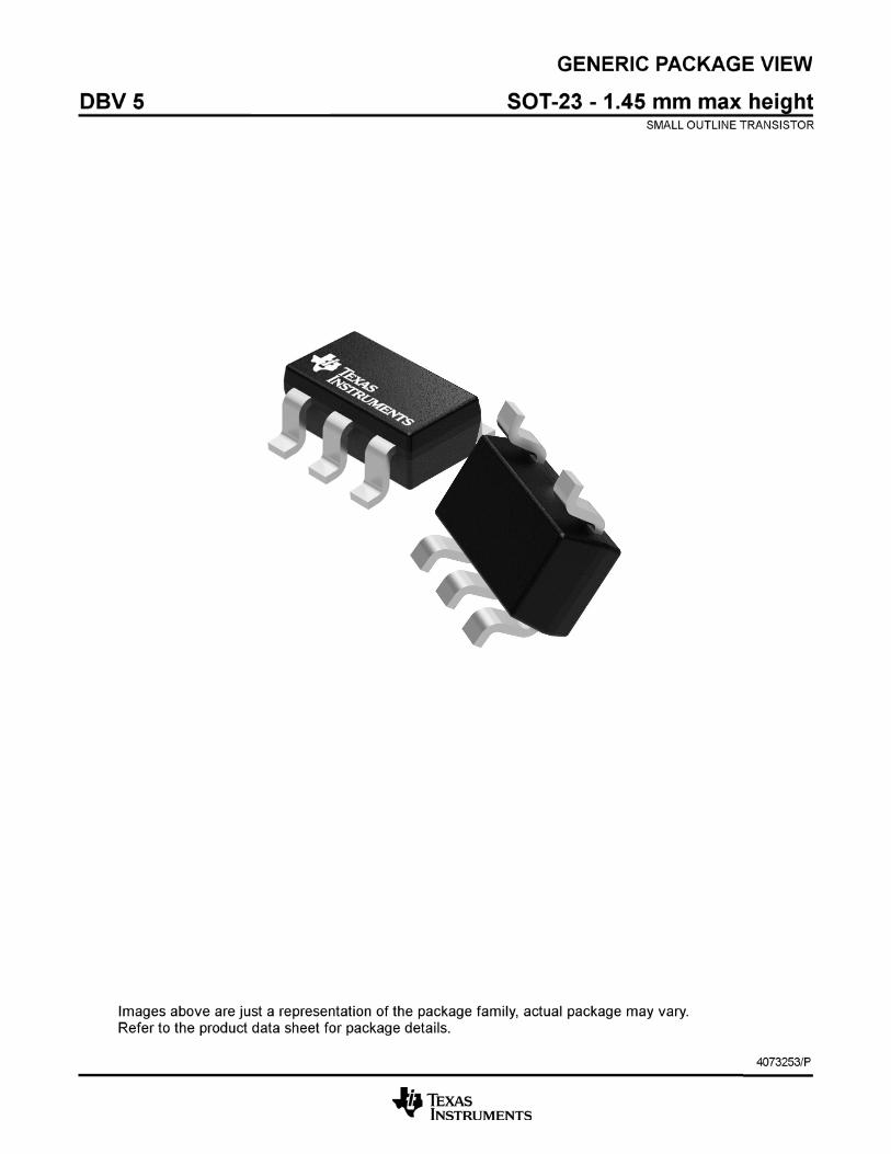
The OPA365-Q1 (single version) is available in the 5-pin SOT-23 package. The OPA2365-Q1 (dual version) isavailable in the 8-pin SOIC package. All versions are specified for operation from −40°C to 125°C. Single anddual versions have identical specifications for maximum design flexibility.
6 Pin Configuration and Functions
DBV Package D Package5-Pin SOT-23 8-Pin SOIC
Top View Top View
Pin FunctionsPIN
I/O DESCRIPTIONNAME SOT-23 SOIC+IN 3 — I Noninverting input–IN 4 — I Inverting input+IN A — 3 I Noninverting input–IN A — 2 I Inverting input+IN B — 5 I Noninverting input–IN B — 6 I Inverting inputV+ 5 8 I Positive (highest) supplyV– 4 4 I Negative (lowest) supplyVOUT I — O OutputVOUTA — 1 O OutputVOUTB — 7 O Output
Copyright © 2010–2015, Texas Instruments Incorporated Submit Documentation Feedback 3
Product Folder Links: OPA365-Q1 OPA2365-Q1
OPA365-Q1, OPA2365-Q1SBOS512D –MARCH 2010–REVISED DECEMBER 2015 www.ti.com
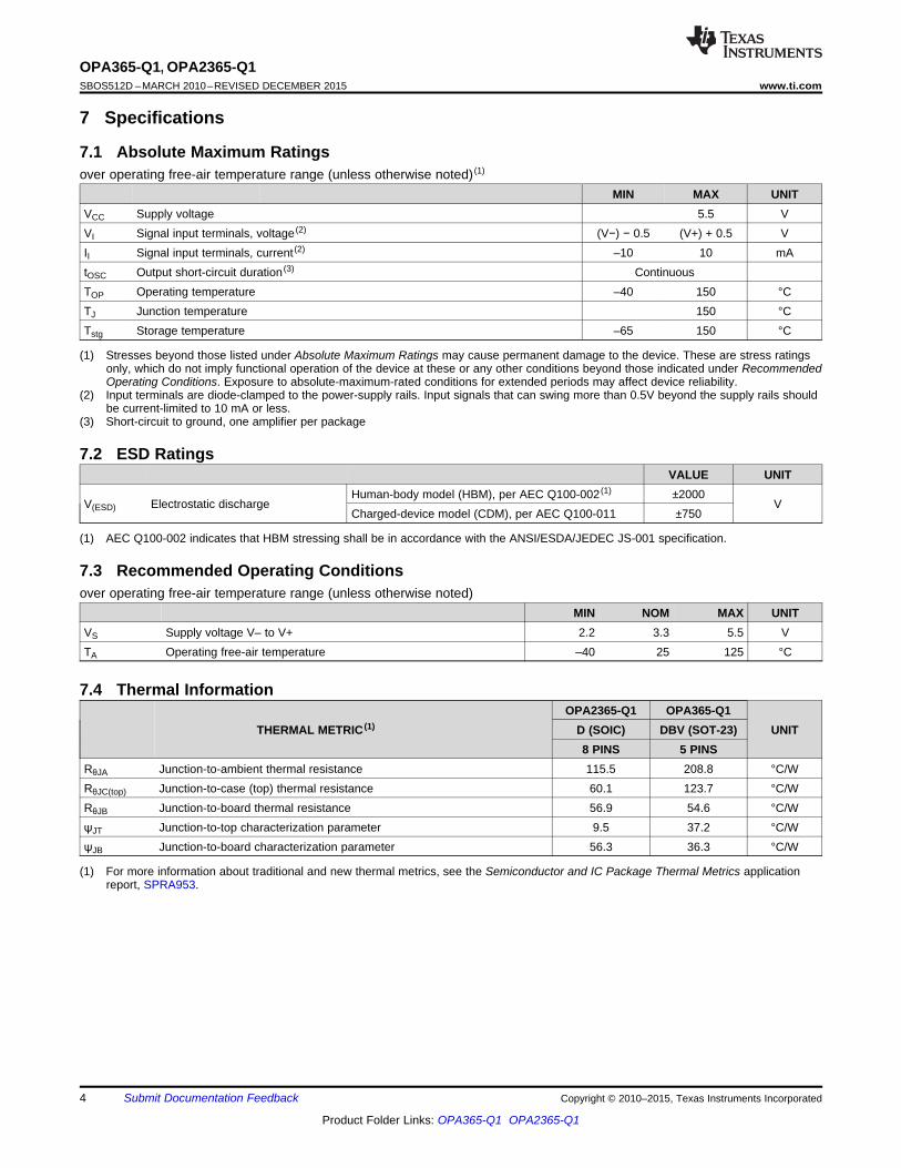
7 Specifications
7.1 Absolute Maximum Ratingsover operating free-air temperature range (unless otherwise noted) (1)
MIN MAX UNITVCC Supply voltage 5.5 VVI Signal input terminals, voltage (2) (V−) − 0.5 (V+) + 0.5 VII Signal input terminals, current (2) –10 10 mAtOSC Output short-circuit duration (3) ContinuousTOP Operating temperature –40 150 °CTJ Junction temperature 150 °CTstg Storage temperature –65 150 °C
(1) Stresses beyond those listed under Absolute Maximum Ratings may cause permanent damage to the device. These are stress ratingsonly, which do not imply functional operation of the device at these or any other conditions beyond those indicated under RecommendedOperating Conditions. Exposure to absolute-maximum-rated conditions for extended periods may affect device reliability.
(2) Input terminals are diode-clamped to the power-supply rails. Input signals that can swing more than 0.5V beyond the supply rails shouldbe current-limited to 10 mA or less.
(3) Short-circuit to ground, one amplifier per package
7.2 ESD RatingsVALUE UNIT
Human-body model (HBM), per AEC Q100-002 (1) ±2000V(ESD) Electrostatic discharge V
Charged-device model (CDM), per AEC Q100-011 ±750
(1) AEC Q100-002 indicates that HBM stressing shall be in accordance with the ANSI/ESDA/JEDEC JS-001 specification.
7.3 Recommended Operating Conditionsover operating free-air temperature range (unless otherwise noted)
MIN NOM MAX UNITVS Supply voltage V– to V+ 2.2 3.3 5.5 VTA Operating free-air temperature –40 25 125 °C
7.4 Thermal InformationOPA2365-Q1 OPA365-Q1
THERMAL METRIC (1) D (SOIC) DBV (SOT-23) UNIT8 PINS 5 PINS
RθJA Junction-to-ambient thermal resistance 115.5 208.8 °C/WRθJC(top) Junction-to-case (top) thermal resistance 60.1 123.7 °C/WRθJB Junction-to-board thermal resistance 56.9 54.6 °C/WψJT Junction-to-top characterization parameter 9.5 37.2 °C/WψJB Junction-to-board characterization parameter 56.3 36.3 °C/W
(1) For more information about traditional and new thermal metrics, see the Semiconductor and IC Package Thermal Metrics applicationreport, SPRA953.
4 Submit Documentation Feedback Copyright © 2010–2015, Texas Instruments Incorporated
Product Folder Links: OPA365-Q1 OPA2365-Q1

OPA365-Q1, OPA2365-Q1www.ti.com SBOS512D –MARCH 2010–REVISED DECEMBER 2015
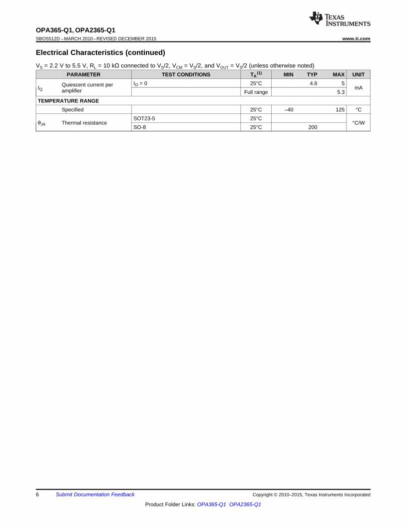
7.5 Electrical CharacteristicsVS = 2.2 V to 5.5 V, RL = 10 kΩ connected to VS/2, VCM = VS/2, and VOUT = VS/2 (unless otherwise noted)
PARAMETER TEST CONDITIONS TA(1) MIN TYP MAX UNIT
OFFSET VOLTAGEVOS Input offset voltage 25°C 100 200 µVVOS
(2) Input offset voltage 25°C 100 230 µVdVOS/ Input offset voltage drift Full range 1 µV/°CdT
Input offset voltage vsPSRR VS = 2.2 V to 5.5 V Full range 10 100 µV/Vpower supplyChannel separation, DC 25°C 0.2 µV/V
INPUT BIAS CURRENT25°C ±0.2 ±10 pA
IB Input bias currentFull range See Typical Characteristics
IOS Input offset current 25°C ±0.2 ±10 pANOISEen Input voltage noise f = 0.1 Hz to 10 Hz 25°C 5 µVPP
en Input voltage noise density f = 100 kHz 25°C 4.5 nV/√Hzin Input current noise density f = 10 kHz 25°C 4 fA/√HzINPUT VOLTAGE RANGE
(V-) – (V+) +VCM Common-mode voltage 25°C V0.1 0.1Common-mode rejectionCMRR (V-) – 0.1 V ≤ VCM ≤ (V+) + 0.1 V Full range 100 120 dBratio
INPUT CAPACITANCEDifferential 25°C 6 pFCommon-mode 25°C 2 pF
OPEN-LOOP GAINRL = 10 kΩ, 100 mV < VO < (V+) – 100 mV Full range 100 120
AOL Open-loop voltage gain RL = 600 Ω, 200 mV < VO < (V+) – 200 mV 25°C 100 120 dBRL = 600 Ω, 200 mV < VO < (V+) – 200 mV Full range 94
FREQUENCY RESPONSEGBW Gain-bandwidth product 25°C 50 MHzSR Slew rate VS = 5 V, G = 1 25°C 25 V/µs
0.1%, VS = 5 V, 4-V Step, G = 1 25°C 200tS Settling time ns
0.01%, VS = 5 V, 4-V Step, G = 1 25°C 300Overload recovery time VS = 5 V, VIN × Gain > VS 25°C < 0.1 µsTotal harmonic distortion + VS = 5 V, RL = 600 Ω, VO = 4 VPP, 0.0004THD+N 25°Cnoise (3) G = 1, f = 1 kHz %
OUTPUTVoltage output swing from RL = 10 kΩ, VS = 5.5 V Full range 10 20 mVrail
ISC Short-circuit current 25°C ±65 mACL Capacitive load drive 25°C See Typical Characteristics
Open-loop output f = 1 MHz, IO = 0 25°C 30 ΩimpedancePOWER SUPPLYVS Specified voltage 25°C 2.2 5.5 V
(1) Full range TA = −40°C to 125°C(2) For OPA2365-Q1 only(3) Third-order filter, bandwidth 80 kHz at −3 dB.
Copyright © 2010–2015, Texas Instruments Incorporated Submit Documentation Feedback 5
Product Folder Links: OPA365-Q1 OPA2365-Q1
OPA365-Q1, OPA2365-Q1SBOS512D –MARCH 2010–REVISED DECEMBER 2015 www.ti.com
Electrical Characteristics (continued)VS = 2.2 V to 5.5 V, RL = 10 kΩ connected to VS/2, VCM = VS/2, and VOUT = VS/2 (unless otherwise noted)
PARAMETER TEST CONDITIONS TA(1) MIN TYP MAX UNIT
IO = 0 25°C 4.6 5Quiescent current perIQ mAamplifier Full range 5.3TEMPERATURE RANGE
Specified 25°C –40 125 °CSOT23-5 25°C
θJA Thermal resistance °C/WSO-8 25°C 200
6 Submit Documentation Feedback Copyright © 2010–2015, Texas Instruments Incorporated
Product Folder Links: OPA365-Q1 OPA2365-Q1
500
400
300
200
100
0−25
I B(p
A)
−0.5 0 5.5
VCM (V)
0.5 1.0 1.5 2.0 2.5 3.0 3.5 4.0 4.5 5.0
VCM Specified RangeInp
utB
ias
(pA
)
1000
900
800
700
600
500
400
300
200
100
0
−25−50
Temperature ( )°C
0 25 50 75 100 125
VS = 5.5V
Offset Voltage (µV)
Po
pu
lation
−2
00
−1
80
−1
60
−1
40
−1
20
−1
00
−80
−60
−40
−20 0
20
40
60
80
10
0
12
0
14
0
16
0
18
0
20
0
Offset Voltage Drift (µV/°C)
Po
pula
tion
0
0.5
1.0
1.5
2.0
2.5
3.0
3.5
4.0
4.5
5.0
Vo
ltage
Ga
in(d
B)
140
120
100
80
60
40
20
0
−20
Phase
(°)
0
−45
−90
−135
−180
1M 10M100k10k1k10010
Frequency (Hz)
100M
Phase
Gain PS
RR
,C
MR
R(d
B)
140
120
100
80
60
40
20
0
1M 10M100k10k1k10010
Frequency (Hz)
100M
CMRR
PSRR
OPA365-Q1, OPA2365-Q1www.ti.com SBOS512D –MARCH 2010–REVISED DECEMBER 2015
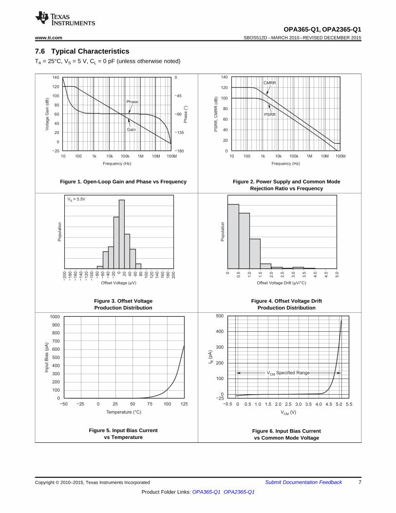
7.6 Typical CharacteristicsTA = 25°C, VS = 5 V, CL = 0 pF (unless otherwise noted)
Figure 1. Open-Loop Gain and Phase vs Frequency Figure 2. Power Supply and Common ModeRejection Ratio vs Frequency
Figure 3. Offset Voltage Figure 4. Offset Voltage DriftProduction Distribution Production Distribution
Figure 5. Input Bias Current Figure 6. Input Bias Currentvs Temperature vs Common Mode Voltage
Copyright © 2010–2015, Texas Instruments Incorporated Submit Documentation Feedback 7
Product Folder Links: OPA365-Q1 OPA2365-Q1

Qu
iescen
tC
urr
ent(m
A)
4.80
4.74
4.68
4.62
4.56
4.50
−25−50
Temperature (°C)
1250 25 50 75 100
2µ
V/d
iv
1s/div
Short
−C
ircuit
Curr
ent
(mA
)
70
60
50
40
30
20
10
0−10−20−30
−40−50−60−70
−80−25−50
Temperature (°C)
1250 25 50 75 100
Dual
VS = ±2.75V
Single
Qu
iescentC
urr
en
t(m
A)
4.75
4.50
4.25
4.00
3.75
2.52.2
Supply Voltage (V)
5.53.0 3.5 4.0 4.5 5.0
Ou
tput
Voltag
e(V
)
3
2
1
0
−1
−2
−3
100
Output Current (mA)
10020 30 40 50 60 70 80 90
+125°C +25°C
−40°C−40°C
+125°C
+25°C
VS = ±1.1V
VS = ±2.75V
Ou
tput
Voltag
e(V
)
3
2
1
0
−1
−2
−3
100
Output Current (mA)
10020 30 40 50 60 70 80 90
+125°C +25°C −40°C
−40°C
+125°C
+25°C
VS = ±1.1V
VS = ±2.75V
OPA365-Q1, OPA2365-Q1SBOS512D –MARCH 2010–REVISED DECEMBER 2015 www.ti.com
Typical Characteristics (continued)TA = 25°C, VS = 5 V, CL = 0 pF (unless otherwise noted)
Figure 7. OPA365-Q1 Output Voltage Figure 8. OPA2365-Q1 Output Voltage Swingvs Output Current vs Output Current
Figure 9. Short-Circuit Current vs Temperature Figure 10. Quiescent Current vs Supply Voltage
Figure 11. Quiescent Current vs Temperature Figure 12. 0.1-Hz to 10-Hz Input Voltage Noise
8 Submit Documentation Feedback Copyright © 2010–2015, Texas Instruments Incorporated
Product Folder Links: OPA365-Q1 OPA2365-Q1

Outp
ut
Voltage
(1V
/div
)
Time (250ns/div)
G = 1
RL = 10kΩ
VS = ±2.5
Outp
ut
Voltag
e(5
0m
V/d
iv)
Time (50ns/div)
G = 1
RL = 600Ω
VS = ±2.5
Overs
hoot
(%)
60
50
40
30
20
10
0
0
Capacitive Load (pF)
1k100
G = +1
G = −1
G = +10
G = −10
Outp
ut
Voltag
e(5
0m
V/d
iv)
Time (50ns/div)
G = 1
RL = 10kΩ
VS = ±2.5V
oltage
Nois
e(n
V/√
Hz)
1k
100
10
1
10k1k10010
Frequency (Hz)
100k
TH
D+
N(%
)
0.01
0.001
0.0001
10k1k10010
Frequency (Hz)
20k
G = 10, RL = 600Ω VO = 1VRMS
VO = 1VRMS
VO = 1.448VRMS
G = +1, RL = 600Ω
OPA365-Q1, OPA2365-Q1www.ti.com SBOS512D –MARCH 2010–REVISED DECEMBER 2015
Typical Characteristics (continued)TA = 25°C, VS = 5 V, CL = 0 pF (unless otherwise noted)
Figure 13. Total Harmonic Distortion Figure 14. Input Voltage Noise Spectral Density+ Noise vs Frequency
Figure 15. Overshoot vs Capacitive Load Figure 16. Small-Signal Step Response
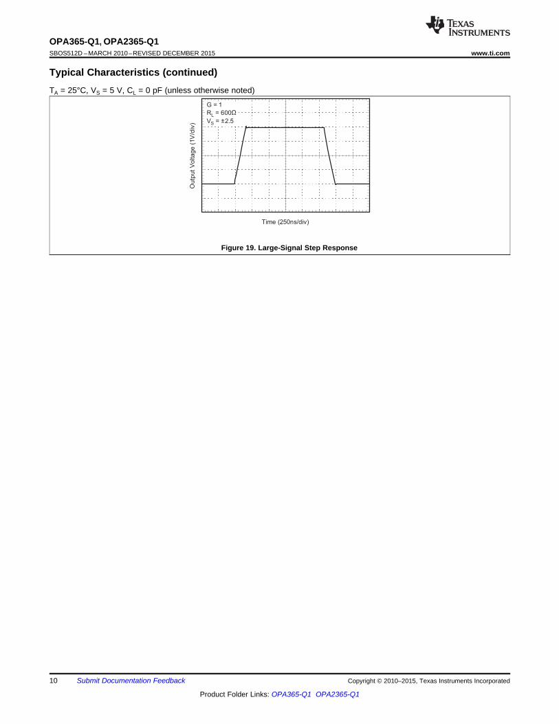
Figure 17. Large-Signal Step Response Figure 18. Small-Signal Step Response
Copyright © 2010–2015, Texas Instruments Incorporated Submit Documentation Feedback 9
Product Folder Links: OPA365-Q1 OPA2365-Q1
Outp
ut
Voltage
(1V
/div
)
Time (250ns/div)
G = 1
RL = 600Ω
VS = ±2.5
OPA365-Q1, OPA2365-Q1SBOS512D –MARCH 2010–REVISED DECEMBER 2015 www.ti.com
Typical Characteristics (continued)TA = 25°C, VS = 5 V, CL = 0 pF (unless otherwise noted)
Figure 19. Large-Signal Step Response
10 Submit Documentation Feedback Copyright © 2010–2015, Texas Instruments Incorporated
Product Folder Links: OPA365-Q1 OPA2365-Q1
Regulated
Charge Pump
VOU T
= VC C
+1.8V
Patent Pending
Very Low Ripple
TopologyIBIA S
VC C
+ 1. 8 V
IBIAS
IBIAS
IBIAS
VS
IBIAS
VOU T
VIN
− VIN
+
OPA365-Q1, OPA2365-Q1www.ti.com SBOS512D –MARCH 2010–REVISED DECEMBER 2015
8 Detailed Description
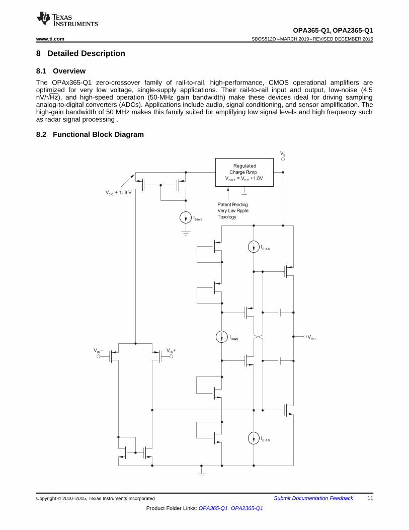
8.1 OverviewThe OPAx365-Q1 zero-crossover family of rail-to-rail, high-performance, CMOS operational amplifiers areoptimized for very low voltage, single-supply applications. Their rail-to-rail input and output, low-noise (4.5nV/√Hz), and high-speed operation (50-MHz gain bandwidth) make these devices ideal for driving samplinganalog-to-digital converters (ADCs). Applications include audio, signal conditioning, and sensor amplification. Thehigh-gain bandwidth of 50 MHz makes this family suited for amplifying low signal levels and high frequency suchas radar signal processing .
8.2 Functional Block Diagram
Copyright © 2010–2015, Texas Instruments Incorporated Submit Documentation Feedback 11
Product Folder Links: OPA365-Q1 OPA2365-Q1
3.3V
49kΩ
VOUTOPA365
Clean 3.3V Supply
1µF
4kΩ
6kΩElectret
Microphone
5kΩ
−1.5V
V−
C1
100nF
C2
100nF
R2
10kΩ
R1
1kΩV+
+1.5V
VOUT
VIN
a) Dual Supply Connection
C1
100nF
R2
10kΩ
R1
1kΩ
V−
V+
+3V
VOUT
V IN
VCM =1.5V
b) Single Supply Connection
OPA365OPA365
OPA365-Q1, OPA2365-Q1SBOS512D –MARCH 2010–REVISED DECEMBER 2015 www.ti.com
8.3 Feature Description
8.3.1 Operating CharacteristicsThe OPA365-Q1 amplifier parameters are fully specified from 2.2 V to 5.5 V. Many of the specifications applyfrom −40°C to 125°C. Parameters that can exhibit significant variance with regard to operating voltage ortemperature are presented in Typical Characteristics.
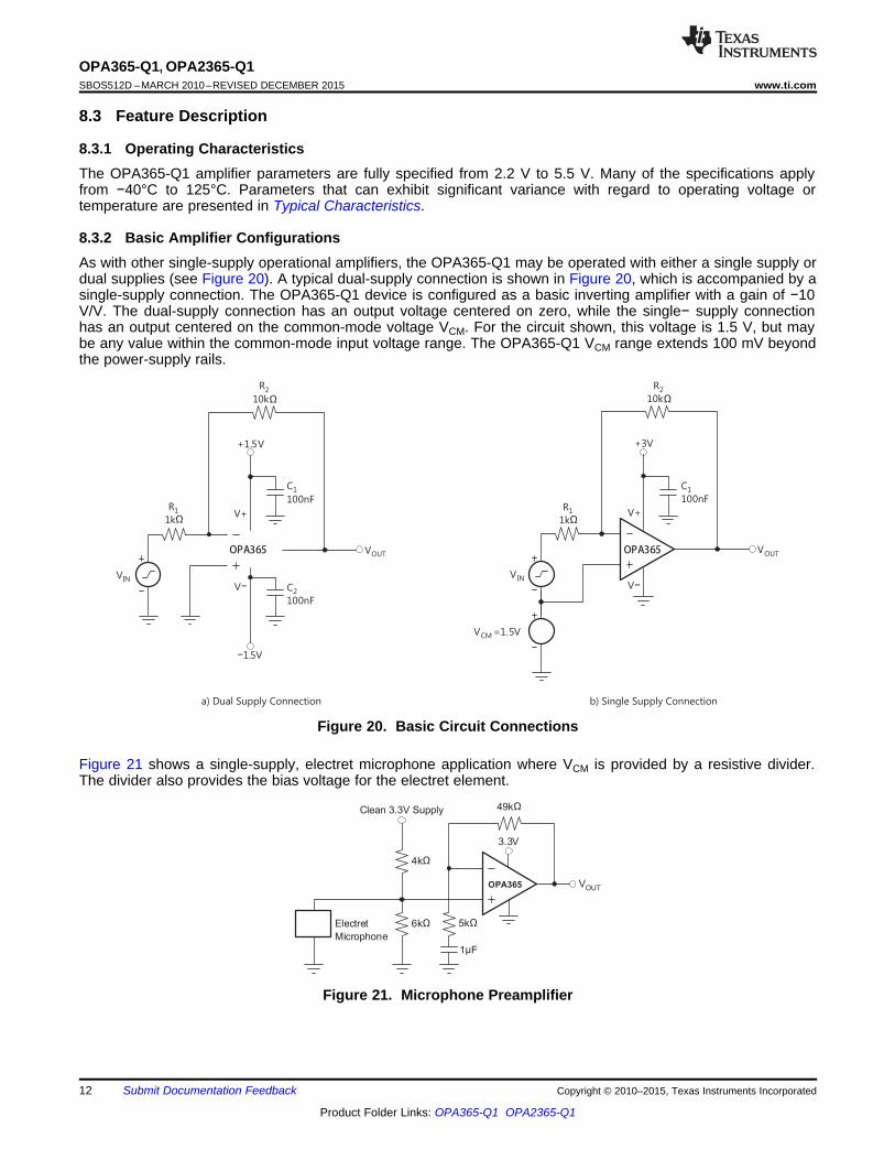
8.3.2 Basic Amplifier ConfigurationsAs with other single-supply operational amplifiers, the OPA365-Q1 may be operated with either a single supply ordual supplies (see Figure 20). A typical dual-supply connection is shown in Figure 20, which is accompanied by asingle-supply connection. The OPA365-Q1 device is configured as a basic inverting amplifier with a gain of −10V/V. The dual-supply connection has an output voltage centered on zero, while the single− supply connectionhas an output centered on the common-mode voltage VCM. For the circuit shown, this voltage is 1.5 V, but maybe any value within the common-mode input voltage range. The OPA365-Q1 VCM range extends 100 mV beyondthe power-supply rails.
Figure 20. Basic Circuit Connections
Figure 21 shows a single-supply, electret microphone application where VCM is provided by a resistive divider.The divider also provides the bias voltage for the electret element.
Figure 21. Microphone Preamplifier
12 Submit Documentation Feedback Copyright © 2010–2015, Texas Instruments Incorporated
Product Folder Links: OPA365-Q1 OPA2365-Q1
OFFSET VOLTAGE vs COMMON MODE VOLTAGE
VO
S(µ
V)
200
150
100
50
0
−50
−150
−100
−200
−2−3
Common Mode Voltage (V)
3−1 0 1 2
V =S±2.75V
OPA365
Competitors
5kΩ
OPA365
10mA max
V+
VIN
VOUT
IOVERLOAD
OPA365-Q1, OPA2365-Q1www.ti.com SBOS512D –MARCH 2010–REVISED DECEMBER 2015
Feature Description (continued)8.3.3 Input and ESD ProtectionThe OPA365-Q1 device incorporates internal electrostatic discharge (ESD) protection circuits on all pins. In thecase of input and output pins, this protection primarily consists of current steering diodes connected between theinput and power-supply pins. These ESD protection diodes also provide in-circuit, input overdrive protection,provided that the current is limited to 10 mA as stated in the Absolute Maximum Ratings. Figure 22 shows how aseries input resistor may be added to the driven input to limit the input current. The added resistor contributesthermal noise at the amplifier input and its value should be kept to the minimum in noise-sensitive applications.
Figure 22. Input Current Protection
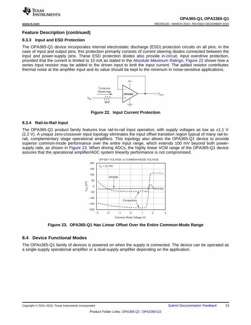
8.3.4 Rail-to-Rail InputThe OPA365-Q1 product family features true rail-to-rail input operation, with supply voltages as low as ±1.1 V(2.2 V). A unique zero-crossover input topology eliminates the input offset transition region typical of many rail-to-rail, complementary stage operational amplifiers. This topology also allows the OPA365-Q1 device to providesuperior common-mode performance over the entire input range, which extends 100 mV beyond both power-supply rails, as shown in Figure 23. When driving ADCs, the highly linear VCM range of the OPA365-Q1 deviceassures that the operational amplifier/ADC system linearity performance is not compromised.
Figure 23. OPA365-Q1 Has Linear Offset Over the Entire Common-Mode Range
8.4 Device Functional ModesThe OPAx365-Q1 family of devices is powered on when the supply is connected. The device can be operated asa single-supply operational amplifier or a dual-supply amplifier depending on the application.
Copyright © 2010–2015, Texas Instruments Incorporated Submit Documentation Feedback 13
Product Folder Links: OPA365-Q1 OPA2365-Q1
10Ω to
20Ω
V+
VIN
VOUT
R
R C
S
L L
OPA365
OPA365-Q1, OPA2365-Q1SBOS512D –MARCH 2010–REVISED DECEMBER 2015 www.ti.com
9 Application and Implementation
NOTEInformation in the following applications sections is not part of the TI componentspecification, and TI does not warrant its accuracy or completeness. TI’s customers areresponsible for determining suitability of components for their purposes. Customers shouldvalidate and test their design implementation to confirm system functionality.
9.1 Application Information
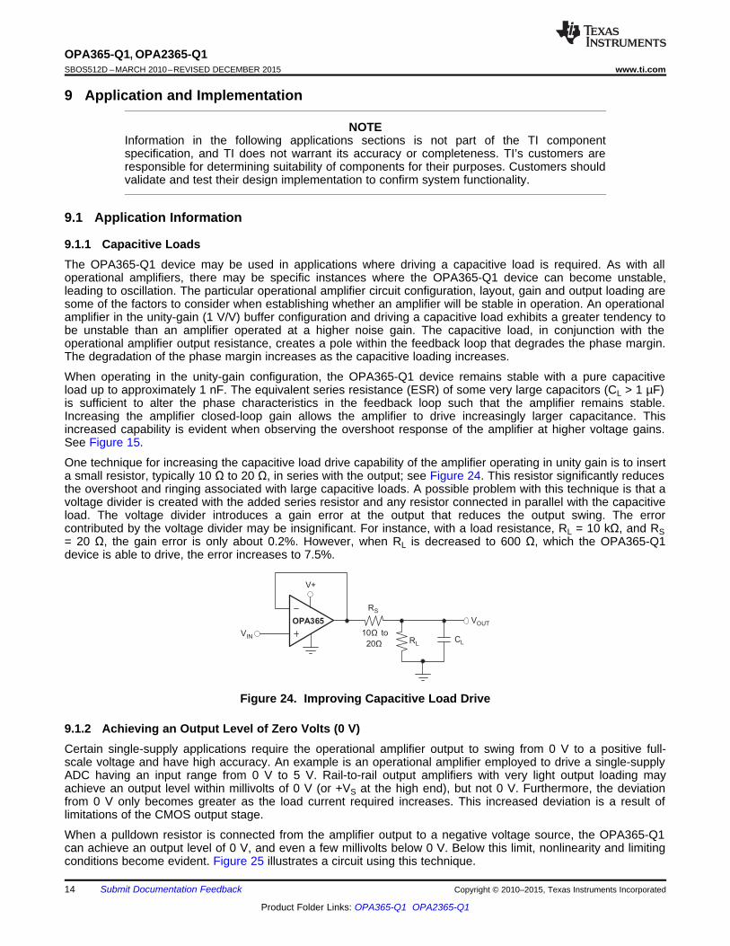
9.1.1 Capacitive LoadsThe OPA365-Q1 device may be used in applications where driving a capacitive load is required. As with alloperational amplifiers, there may be specific instances where the OPA365-Q1 device can become unstable,leading to oscillation. The particular operational amplifier circuit configuration, layout, gain and output loading aresome of the factors to consider when establishing whether an amplifier will be stable in operation. An operationalamplifier in the unity-gain (1 V/V) buffer configuration and driving a capacitive load exhibits a greater tendency tobe unstable than an amplifier operated at a higher noise gain. The capacitive load, in conjunction with theoperational amplifier output resistance, creates a pole within the feedback loop that degrades the phase margin.The degradation of the phase margin increases as the capacitive loading increases.
When operating in the unity-gain configuration, the OPA365-Q1 device remains stable with a pure capacitiveload up to approximately 1 nF. The equivalent series resistance (ESR) of some very large capacitors (CL > 1 µF)is sufficient to alter the phase characteristics in the feedback loop such that the amplifier remains stable.Increasing the amplifier closed-loop gain allows the amplifier to drive increasingly larger capacitance. Thisincreased capability is evident when observing the overshoot response of the amplifier at higher voltage gains.See Figure 15.
One technique for increasing the capacitive load drive capability of the amplifier operating in unity gain is to inserta small resistor, typically 10 Ω to 20 Ω, in series with the output; see Figure 24. This resistor significantly reducesthe overshoot and ringing associated with large capacitive loads. A possible problem with this technique is that avoltage divider is created with the added series resistor and any resistor connected in parallel with the capacitiveload. The voltage divider introduces a gain error at the output that reduces the output swing. The errorcontributed by the voltage divider may be insignificant. For instance, with a load resistance, RL = 10 kΩ, and RS= 20 Ω, the gain error is only about 0.2%. However, when RL is decreased to 600 Ω, which the OPA365-Q1device is able to drive, the error increases to 7.5%.
Figure 24. Improving Capacitive Load Drive
9.1.2 Achieving an Output Level of Zero Volts (0 V)Certain single-supply applications require the operational amplifier output to swing from 0 V to a positive full-scale voltage and have high accuracy. An example is an operational amplifier employed to drive a single-supplyADC having an input range from 0 V to 5 V. Rail-to-rail output amplifiers with very light output loading mayachieve an output level within millivolts of 0 V (or +VS at the high end), but not 0 V. Furthermore, the deviationfrom 0 V only becomes greater as the load current required increases. This increased deviation is a result oflimitations of the CMOS output stage.
When a pulldown resistor is connected from the amplifier output to a negative voltage source, the OPA365-Q1can achieve an output level of 0 V, and even a few millivolts below 0 V. Below this limit, nonlinearity and limitingconditions become evident. Figure 25 illustrates a circuit using this technique.
14 Submit Documentation Feedback Copyright © 2010–2015, Texas Instruments Incorporated
Product Folder Links: OPA365-Q1 OPA2365-Q1
C1
1nF
C2
150pF
R3
549Ω
R1
549Ω
R2
1.24kΩ
V+
VOUT
VIN
V−
OPA365
VOUT
RP = 10 kΩ500µA
OPA365
VIN
V+=+5V
Op AmpNegativeSupply
Grounded−V = −5V
(Additional
Negative Supply)
OPA365-Q1, OPA2365-Q1www.ti.com SBOS512D –MARCH 2010–REVISED DECEMBER 2015
Application Information (continued)
Figure 25. Swing-to-Ground
A pulldown current of approximately 500 µA is required when OPA365-Q1 is connected as a unity-gain buffer. Apractical termination voltage (VNEG) is −5 V, but other convenient negative voltages also may be used. Thepulldown resistor RL is calculated from RL = [(VO −VNEG)/(500 µA)]. Using a minimum output voltage (VO) of 0 V,RL = [0 V−(−5V)]/(500 µA)] = 10 kΩ. Keep in mind that lower termination voltages result in smaller pulldownresistors that load the output during positive output voltage excursions.
This technique does not work with all operational amplifier, and should only be applied to operational amplifiers,such as the OPA365-Q1, that have been specifically designed to operate in this manner. Also, operating theOPA365-Q1 output at 0 V changes the output stage operating conditions, resulting in somewhat lower open-loopgain and bandwidth. Keep these precautions in mind when driving a capacitive load because these conditionscan affect circuit transient response and stability.
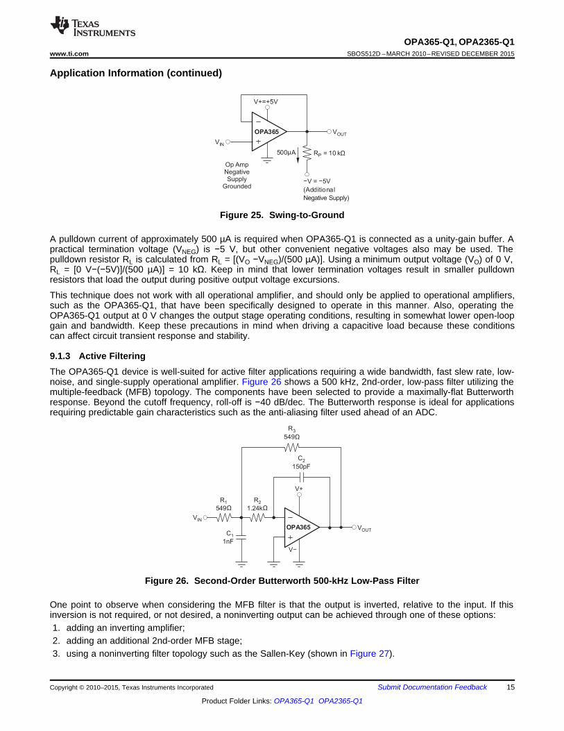
9.1.3 Active FilteringThe OPA365-Q1 device is well-suited for active filter applications requiring a wide bandwidth, fast slew rate, low-noise, and single-supply operational amplifier. Figure 26 shows a 500 kHz, 2nd-order, low-pass filter utilizing themultiple-feedback (MFB) topology. The components have been selected to provide a maximally-flat Butterworthresponse. Beyond the cutoff frequency, roll-off is −40 dB/dec. The Butterworth response is ideal for applicationsrequiring predictable gain characteristics such as the anti-aliasing filter used ahead of an ADC.
Figure 26. Second-Order Butterworth 500-kHz Low-Pass Filter
One point to observe when considering the MFB filter is that the output is inverted, relative to the input. If thisinversion is not required, or not desired, a noninverting output can be achieved through one of these options:1. adding an inverting amplifier;2. adding an additional 2nd-order MFB stage;3. using a noninverting filter topology such as the Sallen-Key (shown in Figure 27).
Copyright © 2010–2015, Texas Instruments Incorporated Submit Documentation Feedback 15
Product Folder Links: OPA365-Q1 OPA2365-Q1
OPA365
–
+
ADS7822-Q1
5 V
0.1µF
100 W
VIN
0 to 4.096 V
1 nF
IN+
IN–
0.1nF
V+
GND
0.1µF
Vref
VOUT
VIN = 1VRMS
OPA365
R3
150kΩ
R2
19.5kΩ
C3
220pF
R1
1.8kΩ
C1
3.3nF
C2
47pF
OPA365-Q1, OPA2365-Q1SBOS512D –MARCH 2010–REVISED DECEMBER 2015 www.ti.com
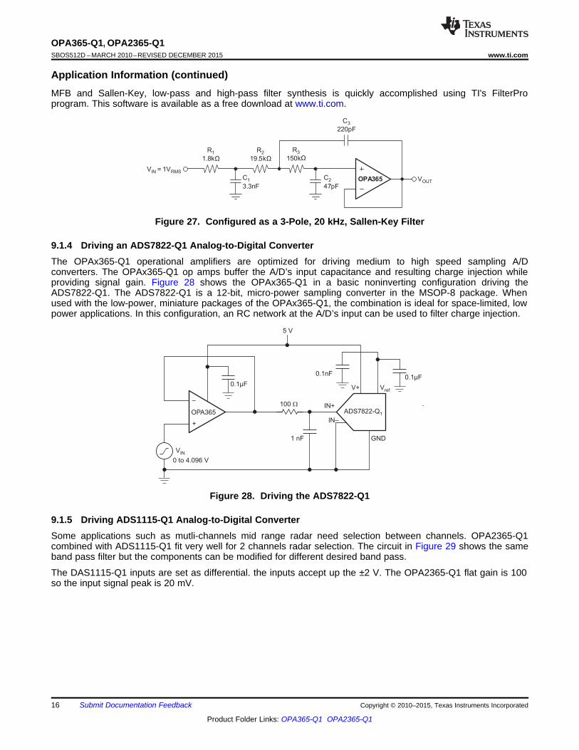
Application Information (continued)MFB and Sallen-Key, low-pass and high-pass filter synthesis is quickly accomplished using TI's FilterProprogram. This software is available as a free download at www.ti.com.
Figure 27. Configured as a 3-Pole, 20 kHz, Sallen-Key Filter
9.1.4 Driving an ADS7822-Q1 Analog-to-Digital ConverterThe OPAx365-Q1 operational amplifiers are optimized for driving medium to high speed sampling A/Dconverters. The OPAx365-Q1 op amps buffer the A/D’s input capacitance and resulting charge injection whileproviding signal gain. Figure 28 shows the OPAx365-Q1 in a basic noninverting configuration driving theADS7822-Q1. The ADS7822-Q1 is a 12-bit, micro-power sampling converter in the MSOP-8 package. Whenused with the low-power, miniature packages of the OPAx365-Q1, the combination is ideal for space-limited, lowpower applications. In this configuration, an RC network at the A/D’s input can be used to filter charge injection.
Figure 28. Driving the ADS7822-Q1
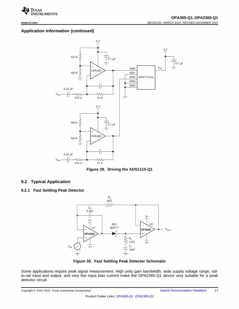
9.1.5 Driving ADS1115-Q1 Analog-to-Digital ConverterSome applications such as mutli-channels mid range radar need selection between channels. OPA2365-Q1combined with ADS1115-Q1 fit very well for 2 channels radar selection. The circuit in Figure 29 shows the sameband pass filter but the components can be modified for different desired band pass.
The DAS1115-Q1 inputs are set as differential. the inputs accept up the ±2 V. The OPA2365-Q1 flat gain is 100so the input signal peak is 20 mV.
16 Submit Documentation Feedback Copyright © 2010–2015, Texas Instruments Incorporated
Product Folder Links: OPA365-Q1 OPA2365-Q1
VIN
VOUT
C2
2.2pF
R2
2kΩ
SD1
BAT17
C1
10nF
R1
7.5Ω
V−
V+
U1
U2
V−
V+
OPA365
OPA365
OPA365
–
+
5 V
0.1 µF100 K
VIN1
AIN0
100 K
51 K
0.22 µF
470 W
ADS1115-Q1
AIN1
AIN2
AIN3
GND
4.7 µF
5 V
OPA365
–
+
5 V
0.1 µF100 K
VIN1
100 K
51 K
0.22 µF
470 W
VDD
OPA365-Q1, OPA2365-Q1www.ti.com SBOS512D –MARCH 2010–REVISED DECEMBER 2015
Application Information (continued)
Figure 29. Driving the ADS1115-Q1
9.2 Typical Application
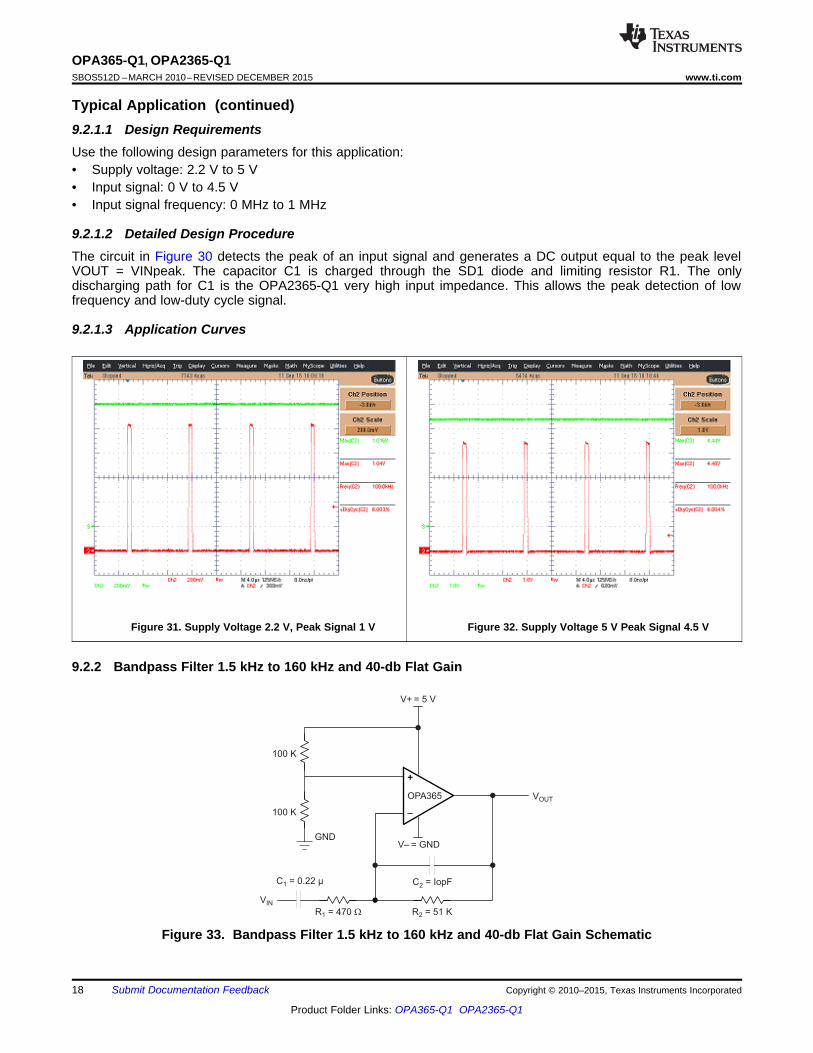
9.2.1 Fast Settling Peak Detector
Figure 30. Fast Settling Peak Detector Schematic
Some applications require peak signal measurement. High unity gain bandwidth, wide supply voltage range, rail-to-rail input and output, and very low input bias current make the OPA2365-Q1 device very suitable for a peakdetector circuit.
Copyright © 2010–2015, Texas Instruments Incorporated Submit Documentation Feedback 17
Product Folder Links: OPA365-Q1 OPA2365-Q1
_
+
V+ = 5 V
C = 0.22 µ1
VOUT
VIN
100 K
OPA365
V– = GND
100 K
GND
C = IopF2
R = 51 K2R = 4701 W
OPA365-Q1, OPA2365-Q1SBOS512D –MARCH 2010–REVISED DECEMBER 2015 www.ti.com
Typical Application (continued)9.2.1.1 Design RequirementsUse the following design parameters for this application:• Supply voltage: 2.2 V to 5 V• Input signal: 0 V to 4.5 V• Input signal frequency: 0 MHz to 1 MHz
9.2.1.2 Detailed Design ProcedureThe circuit in Figure 30 detects the peak of an input signal and generates a DC output equal to the peak levelVOUT = VINpeak. The capacitor C1 is charged through the SD1 diode and limiting resistor R1. The onlydischarging path for C1 is the OPA2365-Q1 very high input impedance. This allows the peak detection of lowfrequency and low-duty cycle signal.
9.2.1.3 Application Curves
Figure 31. Supply Voltage 2.2 V, Peak Signal 1 V Figure 32. Supply Voltage 5 V Peak Signal 4.5 V
9.2.2 Bandpass Filter 1.5 kHz to 160 kHz and 40-db Flat Gain
Figure 33. Bandpass Filter 1.5 kHz to 160 kHz and 40-db Flat Gain Schematic
18 Submit Documentation Feedback Copyright © 2010–2015, Texas Instruments Incorporated
Product Folder Links: OPA365-Q1 OPA2365-Q1

2 2
1A pole at 156 KHz
2 R C= =
p
1 1
1A pole at 1.54 KHz
2 R C= =
p
2 1
1A zero at 14.2 Hz
2 R C= =
p
out 2 1
in 1 1 2 2
V R C SThe transfer function or gain
V (1 R C S) (1 R C S)= = -
+ +
OPA365-Q1, OPA2365-Q1www.ti.com SBOS512D –MARCH 2010–REVISED DECEMBER 2015
Typical Application (continued)9.2.2.1 Design RequirementsUse the following design parameters for this application:• Supply voltage: 2.2 V to 5 V• Input signal: 0 V to 25 mV• Input signal frequency: 0 MHz to 1 MHz
9.2.2.2 Detailed Design ProcedureSome applications need bandpass filter–that is, radar or audio signal precessing. The cross over frequencies andflat gain can be adjusted by changing the resistors and capacitors value according to applications.
The circuit is designed for 5-V supply and 20-mV input signal. With a flat gain of 100 dB or 40 dB, the peakoutput signal is 2 V. The reference signal is at half way of 5 V, which is 2.5 V.
(1)
(2)
(3)
(4)Flat Gain of 100 or 40 dB between 1.54 kHz and 156 kHz (5)20 db/decade below 1.54 KHz (6)–20 dB/decade above 156 kHz (7)Bandpass between 1.54 kHz and 156 kHz (8)
9.2.2.3 Application Curves
Figure 34. Gain Is –3 dB Below the Flat Gain at 1.5 kHz Figure 35. Gain Is –3 dB Above the Flat Gain at 160 kHz
Copyright © 2010–2015, Texas Instruments Incorporated Submit Documentation Feedback 19
Product Folder Links: OPA365-Q1 OPA2365-Q1
NC
±IN
+IN
V±
V+
OUT
NC
NC
VS+
GND
VS±
(or GND for single supply)
GNDOnly needed for
dual-supply
operationGround (GND) plane on another layer
VOUT
VIN
GND
Run the input traces
as far away from
the supply lines
as possible
Use low-ESR, ceramic
bypass capacitor
RF
RG
RIN
Place components
close to device and to
each other to reduce
parasitic errors
+VIN
VOUT
RIN
RG
RF
(Schematic Representation)
OPA365-Q1, OPA2365-Q1SBOS512D –MARCH 2010–REVISED DECEMBER 2015 www.ti.com
10 Power Supply RecommendationsThe OPAx365-Q1 family of devices is specified for operation from 2.2 V to 5.5 V (±1.1 V to ±2.75 V); manyspecifications apply from –40°C to 125°C. The Typical Characteristics presents parameters that can exhibitsignificant variance with regard to operating voltage or temperature.
CAUTIONSupply voltages larger than 7 V can permanently damage the device (see AbsoluteMaximum Ratings).
Place 0.1-μF bypass capacitors close to the power-supply pins to reduce errors coupling in from noisy or highimpedance power supplies. For more detailed information on bypass capacitor placement, see LayoutGuidelines.
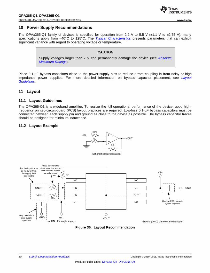
11 Layout
11.1 Layout GuidelinesThe OPA365-Q1 is a wideband amplifier. To realize the full operational performance of the device, good high-frequency printed-circuit-board (PCB) layout practices are required. Low-loss 0.1-µF bypass capacitors must beconnected between each supply pin and ground as close to the device as possible. The bypass capacitor tracesshould be designed for minimum inductance.
11.2 Layout Example
Figure 36. Layout Recommendation
20 Submit Documentation Feedback Copyright © 2010–2015, Texas Instruments Incorporated
Product Folder Links: OPA365-Q1 OPA2365-Q1
OPA365-Q1, OPA2365-Q1www.ti.com SBOS512D –MARCH 2010–REVISED DECEMBER 2015
12 Device and Documentation Support
12.1 Documentation Support
12.1.1 Related DocumentationFor related documentation see the data sheet, ADS1258 16-Channel, 24-Bit Analog-to-Digital Converter(SBAS297).
12.2 Related LinksThe table below lists quick access links. Categories include technical documents, support and communityresources, tools and software, and quick access to sample or buy.
Table 1. Related LinksTECHNICAL TOOLS & SUPPORT &PARTS PRODUCT FOLDER SAMPLE & BUY DOCUMENTS SOFTWARE COMMUNITY
OPA365-Q1 Click here Click here Click here Click here Click hereOPA2365-Q1 Click here Click here Click here Click here Click here
12.3 Community ResourcesThe following links connect to TI community resources. Linked contents are provided "AS IS" by the respectivecontributors. They do not constitute TI specifications and do not necessarily reflect TI's views; see TI's Terms ofUse.
TI E2E™ Online Community TI's Engineer-to-Engineer (E2E) Community. Created to foster collaborationamong engineers. At e2e.ti.com, you can ask questions, share knowledge, explore ideas and helpsolve problems with fellow engineers.
Design Support TI's Design Support Quickly find helpful E2E forums along with design support tools andcontact information for technical support.
12.4 TrademarksE2E is a trademark of Texas Instruments.All other trademarks are the property of their respective owners.
12.5 Electrostatic Discharge CautionThese devices have limited built-in ESD protection. The leads should be shorted together or the device placed in conductive foamduring storage or handling to prevent electrostatic damage to the MOS gates.
12.6 GlossarySLYZ022 — TI Glossary.
This glossary lists and explains terms, acronyms, and definitions.
13 Mechanical, Packaging, and Orderable InformationThe following pages include mechanical, packaging, and orderable information. This information is the mostcurrent data available for the designated devices. This data is subject to change without notice and revision ofthis document. For browser-based versions of this data sheet, refer to the left-hand navigation.
Copyright © 2010–2015, Texas Instruments Incorporated Submit Documentation Feedback 21
Product Folder Links: OPA365-Q1 OPA2365-Q1
PACKAGE OPTION ADDENDUM
www.ti.com 3-Aug-2015
Addendum-Page 1
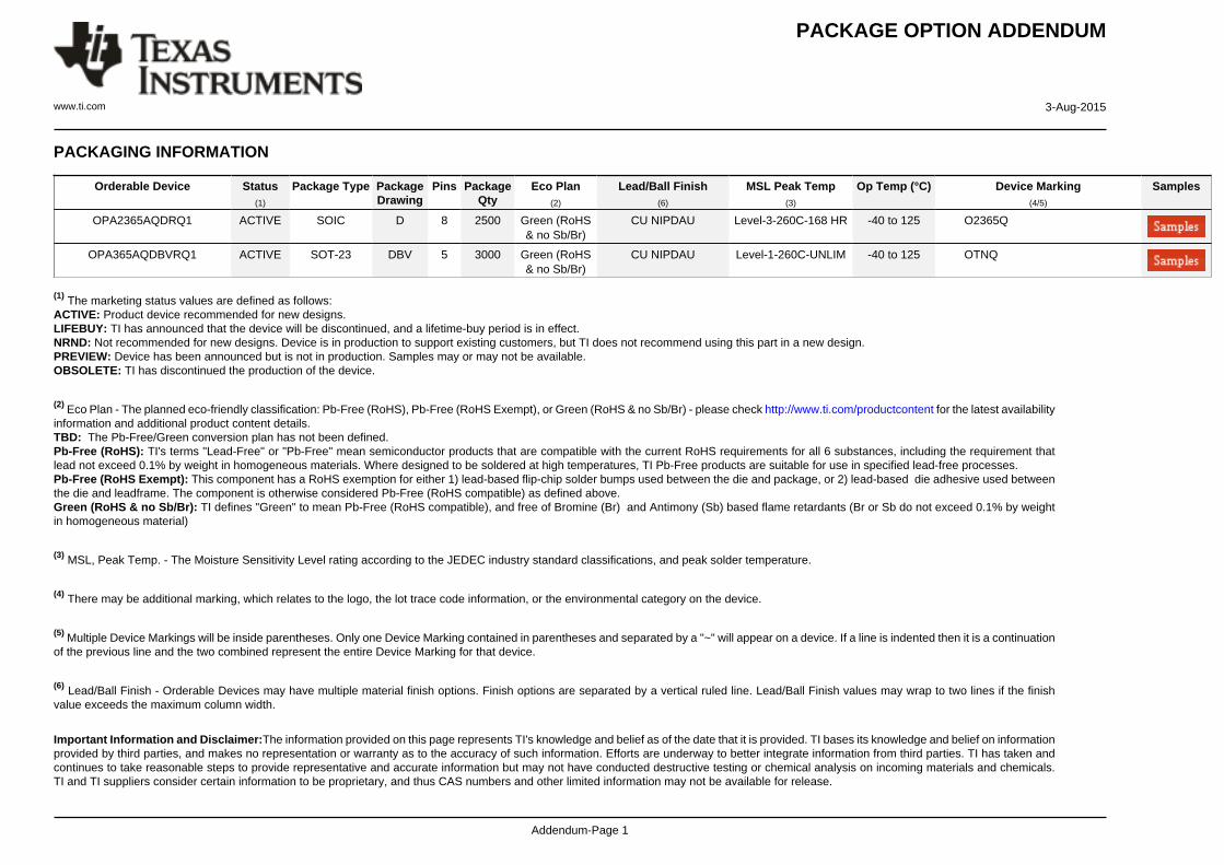
PACKAGING INFORMATION
Orderable Device Status(1)
Package Type PackageDrawing
Pins PackageQty
Eco Plan(2)
Lead/Ball Finish(6)
MSL Peak Temp(3)
Op Temp (°C) Device Marking(4/5)
Samples
OPA2365AQDRQ1 ACTIVE SOIC D 8 2500 Green (RoHS& no Sb/Br)
CU NIPDAU Level-3-260C-168 HR -40 to 125 O2365Q
OPA365AQDBVRQ1 ACTIVE SOT-23 DBV 5 3000 Green (RoHS& no Sb/Br)
CU NIPDAU Level-1-260C-UNLIM -40 to 125 OTNQ
(1) The marketing status values are defined as follows:ACTIVE: Product device recommended for new designs.LIFEBUY: TI has announced that the device will be discontinued, and a lifetime-buy period is in effect.NRND: Not recommended for new designs. Device is in production to support existing customers, but TI does not recommend using this part in a new design.PREVIEW: Device has been announced but is not in production. Samples may or may not be available.OBSOLETE: TI has discontinued the production of the device.
(2) Eco Plan - The planned eco-friendly classification: Pb-Free (RoHS), Pb-Free (RoHS Exempt), or Green (RoHS & no Sb/Br) - please check http://www.ti.com/productcontent for the latest availabilityinformation and additional product content details.TBD: The Pb-Free/Green conversion plan has not been defined.Pb-Free (RoHS): TI's terms "Lead-Free" or "Pb-Free" mean semiconductor products that are compatible with the current RoHS requirements for all 6 substances, including the requirement thatlead not exceed 0.1% by weight in homogeneous materials. Where designed to be soldered at high temperatures, TI Pb-Free products are suitable for use in specified lead-free processes.Pb-Free (RoHS Exempt): This component has a RoHS exemption for either 1) lead-based flip-chip solder bumps used between the die and package, or 2) lead-based die adhesive used betweenthe die and leadframe. The component is otherwise considered Pb-Free (RoHS compatible) as defined above.Green (RoHS & no Sb/Br): TI defines "Green" to mean Pb-Free (RoHS compatible), and free of Bromine (Br) and Antimony (Sb) based flame retardants (Br or Sb do not exceed 0.1% by weightin homogeneous material)
(3) MSL, Peak Temp. - The Moisture Sensitivity Level rating according to the JEDEC industry standard classifications, and peak solder temperature.
(4) There may be additional marking, which relates to the logo, the lot trace code information, or the environmental category on the device.
(5) Multiple Device Markings will be inside parentheses. Only one Device Marking contained in parentheses and separated by a "~" will appear on a device. If a line is indented then it is a continuationof the previous line and the two combined represent the entire Device Marking for that device.
(6) Lead/Ball Finish - Orderable Devices may have multiple material finish options. Finish options are separated by a vertical ruled line. Lead/Ball Finish values may wrap to two lines if the finishvalue exceeds the maximum column width.
Important Information and Disclaimer:The information provided on this page represents TI's knowledge and belief as of the date that it is provided. TI bases its knowledge and belief on informationprovided by third parties, and makes no representation or warranty as to the accuracy of such information. Efforts are underway to better integrate information from third parties. TI has taken andcontinues to take reasonable steps to provide representative and accurate information but may not have conducted destructive testing or chemical analysis on incoming materials and chemicals.TI and TI suppliers consider certain information to be proprietary, and thus CAS numbers and other limited information may not be available for release.

PACKAGE OPTION ADDENDUM
www.ti.com 3-Aug-2015
Addendum-Page 2
In no event shall TI's liability arising out of such information exceed the total purchase price of the TI part(s) at issue in this document sold by TI to Customer on an annual basis.
OTHER QUALIFIED VERSIONS OF OPA2365-Q1, OPA365-Q1 :
• Catalog: OPA2365, OPA365
• Enhanced Product: OPA365-EP
NOTE: Qualified Version Definitions:
• Catalog - TI's standard catalog product
• Enhanced Product - Supports Defense, Aerospace and Medical Applications

TAPE AND REEL INFORMATION
*All dimensions are nominal
Device PackageType
PackageDrawing
Pins SPQ ReelDiameter
(mm)
ReelWidth
W1 (mm)
A0(mm)
B0(mm)
K0(mm)
P1(mm)
W(mm)
Pin1Quadrant
OPA2365AQDRQ1 SOIC D 8 2500 330.0 12.4 6.4 5.2 2.1 8.0 12.0 Q1
OPA365AQDBVRQ1 SOT-23 DBV 5 3000 179.0 8.4 3.2 3.2 1.4 4.0 8.0 Q3
PACKAGE MATERIALS INFORMATION
www.ti.com 3-Aug-2017
Pack Materials-Page 1
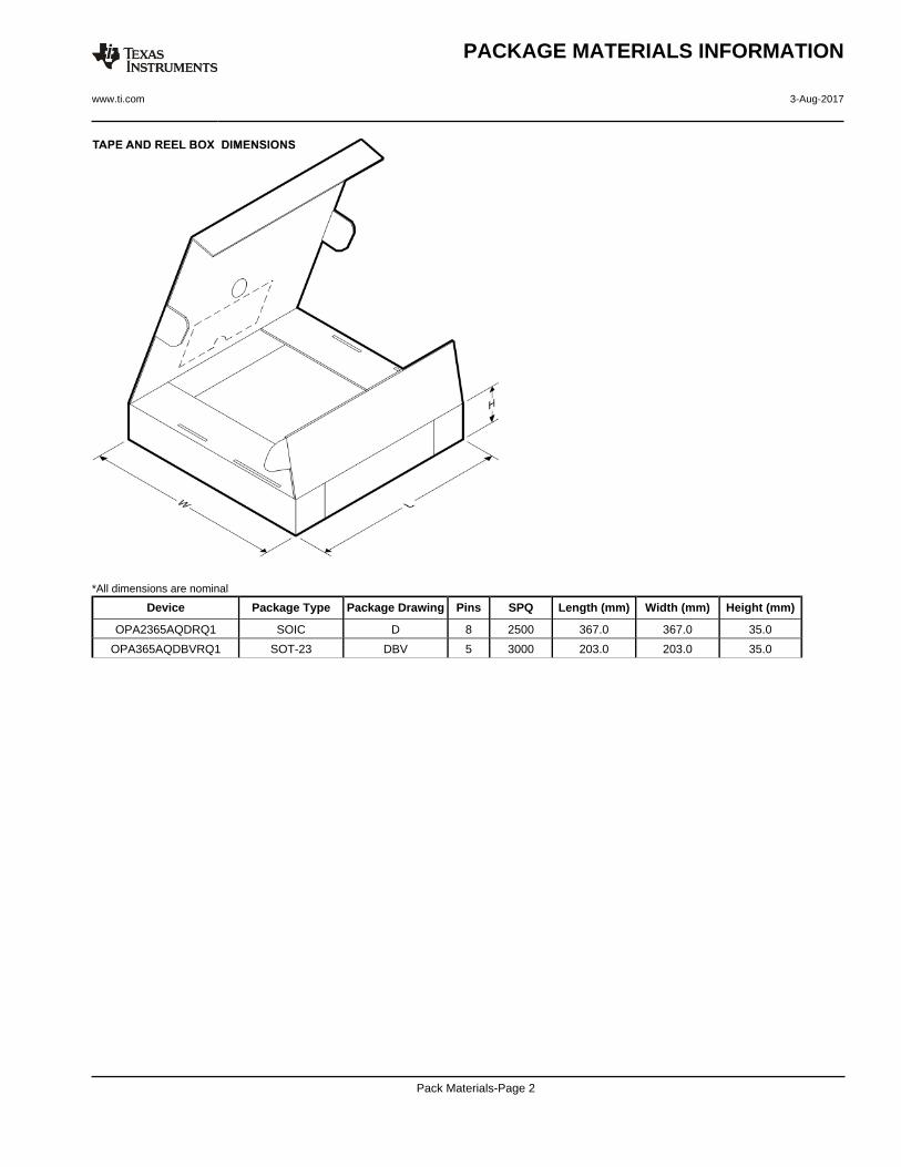
*All dimensions are nominal
Device Package Type Package Drawing Pins SPQ Length (mm) Width (mm) Height (mm)
OPA2365AQDRQ1 SOIC D 8 2500 367.0 367.0 35.0
OPA365AQDBVRQ1 SOT-23 DBV 5 3000 203.0 203.0 35.0
PACKAGE MATERIALS INFORMATION
www.ti.com 3-Aug-2017
Pack Materials-Page 2
www.ti.com
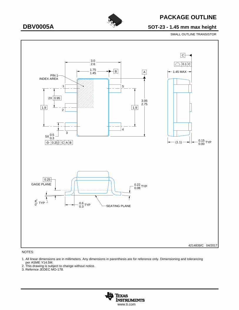
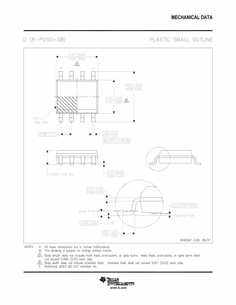
PACKAGE OUTLINE
C
TYP0.220.08
0.25
3.02.6
2X 0.95
1.9
1.45 MAX
TYP0.150.00
5X 0.50.3
TYP0.60.3
TYP80
1.9
A
3.052.75
B1.751.45
(1.1)
SOT-23 - 1.45 mm max heightDBV0005ASMALL OUTLINE TRANSISTOR
4214839/C 04/2017
NOTES: 1. All linear dimensions are in millimeters. Any dimensions in parenthesis are for reference only. Dimensioning and tolerancing per ASME Y14.5M.2. This drawing is subject to change without notice.3. Refernce JEDEC MO-178.
0.2 C A B
1
34
5
2
INDEX AREAPIN 1
GAGE PLANE
SEATING PLANE
0.1 C
SCALE 4.000

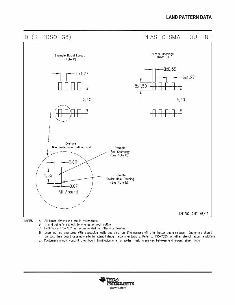
www.ti.com
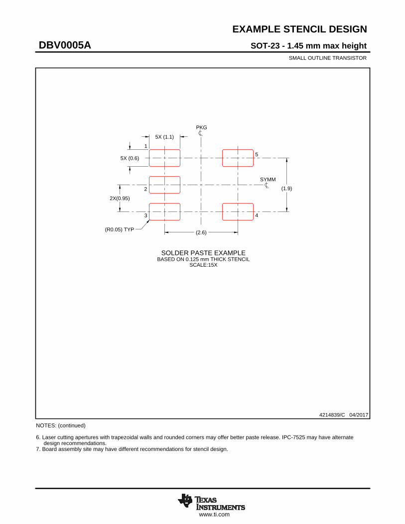
EXAMPLE BOARD LAYOUT
0.07 MAXARROUND
0.07 MINARROUND
5X (1.1)
5X (0.6)
(2.6)
(1.9)
2X (0.95)
(R0.05) TYP
4214839/C 04/2017
SOT-23 - 1.45 mm max heightDBV0005ASMALL OUTLINE TRANSISTOR
NOTES: (continued) 4. Publication IPC-7351 may have alternate designs. 5. Solder mask tolerances between and around signal pads can vary based on board fabrication site.
SYMM
LAND PATTERN EXAMPLEEXPOSED METAL SHOWN
SCALE:15X
PKG
1
3 4
5
2
SOLDER MASKOPENINGMETAL UNDER
SOLDER MASK
SOLDER MASKDEFINED
EXPOSED METAL
METALSOLDER MASKOPENING
NON SOLDER MASKDEFINED
(PREFERRED)
SOLDER MASK DETAILS
EXPOSED METAL
www.ti.com
EXAMPLE STENCIL DESIGN
(2.6)
(1.9)
2X(0.95)
5X (1.1)
5X (0.6)
(R0.05) TYP
SOT-23 - 1.45 mm max heightDBV0005ASMALL OUTLINE TRANSISTOR
4214839/C 04/2017
NOTES: (continued) 6. Laser cutting apertures with trapezoidal walls and rounded corners may offer better paste release. IPC-7525 may have alternate design recommendations. 7. Board assembly site may have different recommendations for stencil design.
SOLDER PASTE EXAMPLEBASED ON 0.125 mm THICK STENCIL
SCALE:15X
SYMM
PKG
1
3 4
5
2
IMPORTANT NOTICE
Texas Instruments Incorporated (TI) reserves the right to make corrections, enhancements, improvements and other changes to itssemiconductor products and services per JESD46, latest issue, and to discontinue any product or service per JESD48, latest issue. Buyersshould obtain the latest relevant information before placing orders and should verify that such information is current and complete.TI’s published terms of sale for semiconductor products (http://www.ti.com/sc/docs/stdterms.htm) apply to the sale of packaged integratedcircuit products that TI has qualified and released to market. Additional terms may apply to the use or sale of other types of TI products andservices.Reproduction of significant portions of TI information in TI data sheets is permissible only if reproduction is without alteration and isaccompanied by all associated warranties, conditions, limitations, and notices. TI is not responsible or liable for such reproduceddocumentation. Information of third parties may be subject to additional restrictions. Resale of TI products or services with statementsdifferent from or beyond the parameters stated by TI for that product or service voids all express and any implied warranties for theassociated TI product or service and is an unfair and deceptive business practice. TI is not responsible or liable for any such statements.Buyers and others who are developing systems that incorporate TI products (collectively, “Designers”) understand and agree that Designersremain responsible for using their independent analysis, evaluation and judgment in designing their applications and that Designers havefull and exclusive responsibility to assure the safety of Designers' applications and compliance of their applications (and of all TI productsused in or for Designers’ applications) with all applicable regulations, laws and other applicable requirements. Designer represents that, withrespect to their applications, Designer has all the necessary expertise to create and implement safeguards that (1) anticipate dangerousconsequences of failures, (2) monitor failures and their consequences, and (3) lessen the likelihood of failures that might cause harm andtake appropriate actions. Designer agrees that prior to using or distributing any applications that include TI products, Designer willthoroughly test such applications and the functionality of such TI products as used in such applications.TI’s provision of technical, application or other design advice, quality characterization, reliability data or other services or information,including, but not limited to, reference designs and materials relating to evaluation modules, (collectively, “TI Resources”) are intended toassist designers who are developing applications that incorporate TI products; by downloading, accessing or using TI Resources in anyway, Designer (individually or, if Designer is acting on behalf of a company, Designer’s company) agrees to use any particular TI Resourcesolely for this purpose and subject to the terms of this Notice.TI’s provision of TI Resources does not expand or otherwise alter TI’s applicable published warranties or warranty disclaimers for TIproducts, and no additional obligations or liabilities arise from TI providing such TI Resources. TI reserves the right to make corrections,enhancements, improvements and other changes to its TI Resources. TI has not conducted any testing other than that specificallydescribed in the published documentation for a particular TI Resource.Designer is authorized to use, copy and modify any individual TI Resource only in connection with the development of applications thatinclude the TI product(s) identified in such TI Resource. NO OTHER LICENSE, EXPRESS OR IMPLIED, BY ESTOPPEL OR OTHERWISETO ANY OTHER TI INTELLECTUAL PROPERTY RIGHT, AND NO LICENSE TO ANY TECHNOLOGY OR INTELLECTUAL PROPERTYRIGHT OF TI OR ANY THIRD PARTY IS GRANTED HEREIN, including but not limited to any patent right, copyright, mask work right, orother intellectual property right relating to any combination, machine, or process in which TI products or services are used. Informationregarding or referencing third-party products or services does not constitute a license to use such products or services, or a warranty orendorsement thereof. Use of TI Resources may require a license from a third party under the patents or other intellectual property of thethird party, or a license from TI under the patents or other intellectual property of TI.TI RESOURCES ARE PROVIDED “AS IS” AND WITH ALL FAULTS. TI DISCLAIMS ALL OTHER WARRANTIES ORREPRESENTATIONS, EXPRESS OR IMPLIED, REGARDING RESOURCES OR USE THEREOF, INCLUDING BUT NOT LIMITED TOACCURACY OR COMPLETENESS, TITLE, ANY EPIDEMIC FAILURE WARRANTY AND ANY IMPLIED WARRANTIES OFMERCHANTABILITY, FITNESS FOR A PARTICULAR PURPOSE, AND NON-INFRINGEMENT OF ANY THIRD PARTY INTELLECTUALPROPERTY RIGHTS. TI SHALL NOT BE LIABLE FOR AND SHALL NOT DEFEND OR INDEMNIFY DESIGNER AGAINST ANY CLAIM,INCLUDING BUT NOT LIMITED TO ANY INFRINGEMENT CLAIM THAT RELATES TO OR IS BASED ON ANY COMBINATION OFPRODUCTS EVEN IF DESCRIBED IN TI RESOURCES OR OTHERWISE. IN NO EVENT SHALL TI BE LIABLE FOR ANY ACTUAL,DIRECT, SPECIAL, COLLATERAL, INDIRECT, PUNITIVE, INCIDENTAL, CONSEQUENTIAL OR EXEMPLARY DAMAGES INCONNECTION WITH OR ARISING OUT OF TI RESOURCES OR USE THEREOF, AND REGARDLESS OF WHETHER TI HAS BEENADVISED OF THE POSSIBILITY OF SUCH DAMAGES.Unless TI has explicitly designated an individual product as meeting the requirements of a particular industry standard (e.g., ISO/TS 16949and ISO 26262), TI is not responsible for any failure to meet such industry standard requirements.Where TI specifically promotes products as facilitating functional safety or as compliant with industry functional safety standards, suchproducts are intended to help enable customers to design and create their own applications that meet applicable functional safety standardsand requirements. Using products in an application does not by itself establish any safety features in the application. Designers mustensure compliance with safety-related requirements and standards applicable to their applications. Designer may not use any TI products inlife-critical medical equipment unless authorized officers of the parties have executed a special contract specifically governing such use.Life-critical medical equipment is medical equipment where failure of such equipment would cause serious bodily injury or death (e.g., lifesupport, pacemakers, defibrillators, heart pumps, neurostimulators, and implantables). Such equipment includes, without limitation, allmedical devices identified by the U.S. Food and Drug Administration as Class III devices and equivalent classifications outside the U.S.TI may expressly designate certain products as completing a particular qualification (e.g., Q100, Military Grade, or Enhanced Product).Designers agree that it has the necessary expertise to select the product with the appropriate qualification designation for their applicationsand that proper product selection is at Designers’ own risk. Designers are solely responsible for compliance with all legal and regulatoryrequirements in connection with such selection.Designer will fully indemnify TI and its representatives against any damages, costs, losses, and/or liabilities arising out of Designer’s non-compliance with the terms and provisions of this Notice.
Mailing Address: Texas Instruments, Post Office Box 655303, Dallas, Texas 75265Copyright © 2018, Texas Instruments Incorporated


![Influence Maximization with -Almost Submodular Threshold ... · PDF fileprovide (1 ")‘(1 1=e) ... For a directed graph G= (V;E), ... vuniformly at random from the interval [0;1].](https://static.fdocument.org/doc/165x107/5a8886f87f8b9a882e8e4480/inuence-maximization-with-almost-submodular-threshold-1-1-1e-.jpg)